Review

Nanoelectromechanical Switches for Low-Power Digital Computing

Department of Electrical Engineering and Computer Sciences, University of California, Berkeley, CA 94720, USA
*
Authors to whom correspondence should be addressed.
These authors contributed equally to this work.
Micromachines 2015, 6(8), 1046-1065; https://doi.org/10.3390/mi6081046
Submission received: 1 July 2015 / Revised: 1 July 2015 / Accepted: 4 August 2015 / Published: 10 August 2015
(This article belongs to the Special Issue CMOS-MEMS Sensors and Devices)

Abstract

:
The need for more energy-efficient solid-state switches beyond complementary metal-oxide-semiconductor (CMOS) transistors has become a major concern as the power consumption of electronic integrated circuits (ICs) steadily increases with technology scaling. Nano-Electro-Mechanical (NEM) relays control current flow by nanometer-scale motion to make or break physical contact between electrodes, and offer advantages over transistors for low-power digital logic applications: virtually zero leakage current for negligible static power consumption; the ability to operate with very small voltage signals for low dynamic power consumption; and robustness against harsh environments such as extreme temperatures. Therefore, NEM logic switches (relays) have been investigated by several research groups during the past decade. Circuit simulations calibrated to experimental data indicate that scaled relay technology can overcome the energy-efficiency limit of CMOS technology. This paper reviews recent progress toward this goal, providing an overview of the different relay designs and experimental results achieved by various research groups, as well as of relay-based IC design principles. Remaining challenges for realizing the promise of nano-mechanical computing, and ongoing efforts to address these, are discussed.

1. Introduction

Over the past five decades, steady progress in planar processing technology to manufacture transistors with ever smaller dimensions has provided exponential growth in the number of components (transistors) and, hence, the functionality of integrated circuit (IC) “chips” over time, according to Moore’s Law [1]. In the most recent decade, however, the transistor operating voltage (VDD) has not been reduced proportionately with the transistor size (Figure 1) [2]; therefore, as the number and density of transistors on a chip have increased, the peak power density also has increased [3]. Due to limitations of chip cooling technology, either IC blocks must be periodically powered down (disconnected from the power supply) or the digital logic circuits must be operated at slower speeds with parallelism (e.g., multi-core processing) used to achieve improvements in system performance [4]. The root cause of this chip power crisis is transistor OFF-state leakage current (IOFF), as explained below.
Figure 2a illustrates the basic metal-oxide-semiconductor field-effect transistor (MOSFET) structure, which is essentially a three-terminal solid-state switch: when a sufficiently large voltage (greater than a “threshold voltage” VTH) is applied to the metallic gate electrode, the transistor is in the ON state and electric current can readily flow through the semiconductor channel region between the heavily doped (electrically conductive) semiconductor source and drain regions (Note that the gate electrode is electrically insulated from the channel region by a thin insulating oxide layer so that no direct current flows between the gate and semiconductor). In the sub-threshold regime of operation, the current (ID) decreases exponentially with decreasing gate voltage (VG) below VTH, reaching IOFF at VG = 0 V, as illustrated in Figure 2b; the rate at which the current changes is defined as the subthreshold swing (SS), i.e., IOFF is proportional to 10VTH/SS. The static power consumption of a digital logic circuit is proportional to IOFF; this has limited VTH scaling and, hence, VDD scaling, since the peak MOSFET ON-state current (hence the circuit operating speed) is a super-linear function of VDDVTH.
To mitigate the chip power crisis, MOSFET design improvements which provide for high ON-state currents (ION) at a lower VG have been adopted in recent years. Strained silicon technology is used to boost the mobility of mobile charge carriers in the silicon channel region and, hence, ION [5]. High-permittivity (high-k) dielectric material is incorporated into the gate-insulating layer [6] to provide for improved capacitive coupling between the gate electrode and channel region, to steepen the subthreshold swing so that VTH is lower for a given IOFF specification. Thin-body transistor structures such as the fully depleted silicon-on-insulator (FDSOI) MOSFET [7] and the three-dimensional (3-D) FinFET [8,9] provide for even better gate control and steeper subthreshold swing. SS is fundamentally limited to be no less than ln(10) × kBT/q = 60 mV/dec at room temperature, however, due to the Fermi-Dirac energy distribution of electrons in the semiconductor source region. Because of this fundamental limitation of the MOSFET, alternative logic switch designs are needed to enable further reductions in chip operating voltage.
Tunneling has been proposed as a current conduction mechanism that can be switched more abruptly than thermionic emission (in a MOSFET) [10,11]. Tunneling FET (TFET) devices have been experimentally demonstrated with sub-60 mV/dec subthreshold swing [12,13], but generally have exhibited relatively poor ON/OFF current ratio for gate voltage swing below 1 V. A mechanical switch is ideal in that it has zero IOFF and abrupt switching behavior which, in principle, allows VTH and, hence, VDD to be scaled down aggressively while maintaining high conductance in the ON state (limited by the physical contact resistance). The use of mechanical switches for computing is not a new idea, and dates back to the 1930s [14]. Due to advancements in planar processing technology over the past few decades, particularly the development of surface micromachining processes for micro-electro-mechanical systems (MEMS) [15], there has been renewed interest in mechanical computing for ultra-low-power digital logic applications [16,17]. This paper reviews recent work toward the goal of achieving nano-electro-mechanical (NEM) logic switches suitable for low-power computing. The following sections will provide an overview of different relay designs and experimental results achieved by various research groups, and of relay-based IC design principles. Remaining challenges for realizing the promise of mechanical computing, and ongoing efforts to address these, are discussed.
Figure 1. Trends for metal-oxide-semiconductor field-effect transistor (MOSFET) threshold voltage (VTH) and operating voltage (VDD), and corresponding transistor OFF-state leakage (IOFF), for high-performance digital logic [2].
Micromachines 06 01046 g001
Figure 2. Schematic illustrations of the MOSFET (a) structure, (b) transfer characteristics (output current ID vs. input voltage VG). If the operating voltage (VDD) is to be reduced, then the threshold voltage (VTH) should be reduced (i.e., the I-V curve should be shifted to the left) to maintain the same peak level of ON-state current, but this would result in an exponential increase in OFF-state leakage current (IOFF).
Micromachines 06 01046 g002

2. Brief Overview of Logic Relay Technologies

Relays use the mechanical motion of a movable electrode (beam or membrane) to make/break physical contact between two electrically conductive electrodes in order to switch current ON/OFF. The first MEM relay was demonstrated by Petersen in 1979 [18]. In subsequent years, various types of relays have been investigated and can be classified according to their actuation mechanism [19]. Thermal relays use different thermal expansion coefficients of two materials to bend a cantilever under the effect of heating. Magnetic relays use ferromagnetic material in the movable electrode to actuate it with the application of a magnetic field. Piezoelectric relays use the deformation of a piezoelectric material under the effect of an electric field. Electrostatic relays directly use the effect of an electric field to actuate a suspended electrode with an applied voltage. Commercial applications of MEM switches include automated test equipment, wide band systems, and tunable antennas [20].
The need for a very small device footprint and fast switching speed makes thermal actuation and magnetic actuation unsuitable for digital logic applications. Piezoelectric relays have been demonstrated in the works of Zaghloul and Piazza at Carnegie Mellon University. They used a stack of ultra-thin (10 nm) AlN layers sandwiched between metallic electrodes [21,22,23]. The actuation voltage is around 520 mV and the relay can even switch with voltages as low as 20 mV (by applying a bias voltage to the substrate), which is the smallest pull-in voltage reported for a logic relay to date. However, the footprint is around 58 µm2 for the smallest device. Piezoelectric devices are difficult to scale down to a very small size.
Electrostatic switches of various designs have been reported in the literature, with the number of terminals ranging from two up to six. A minimum of three (one control and two output) terminals is required for a logic relay. Figure 3 shows a schematic of a basic three-terminal (3T) relay in which the input voltage signal is applied to the fixed “gate” terminal and the output current signal flows between the movable “source” terminal and the fixed “drain” terminal. In the following section, the operation and properties of this basic electrostatic relay are described in more detail.
Figure 3. Illustration of an electrostatic 3T relay: (a) as fabricated, (b) actuated into the ON state.
Micromachines 06 01046 g003

3. Electrostatic Relay Basics

3.1. Benefits for Digital Logic Applications

Compared with the MOSFET, the electrostatic relay offers many advantages. First, there is a significant reduction in standby power consumption, since leakage current is negligible due to the physical separation of the two conductive electrodes in the OFF state. Second, there is abrupt switching behavior, with SS ≈ 0 (Figure 4a), which enables very small operating voltage swing, potentially as low as ~10 mV (determined by the hysteresis voltage) [24]. These two advantages make nano-electro-mechanical (NEM) relay-based circuits potentially more energy efficient than their complementary metal-oxide-semiconductor (CMOS) counterparts [16,17]. Since MOSFETs are superior for high-speed switching, hybrid CMOS/NEM relay circuits show the most promise for achieving a good balance of energy efficiency and information processing throughput. NEM relays are also less sensitive than MOSFETs to radiation, which makes them advantageous for aerospace and military applications.
Figure 4. (a) Electrical characteristics of a nano-electro-mechanical (NEM) relay. (b) Spring model of a NEM relay.
Micromachines 06 01046 g004

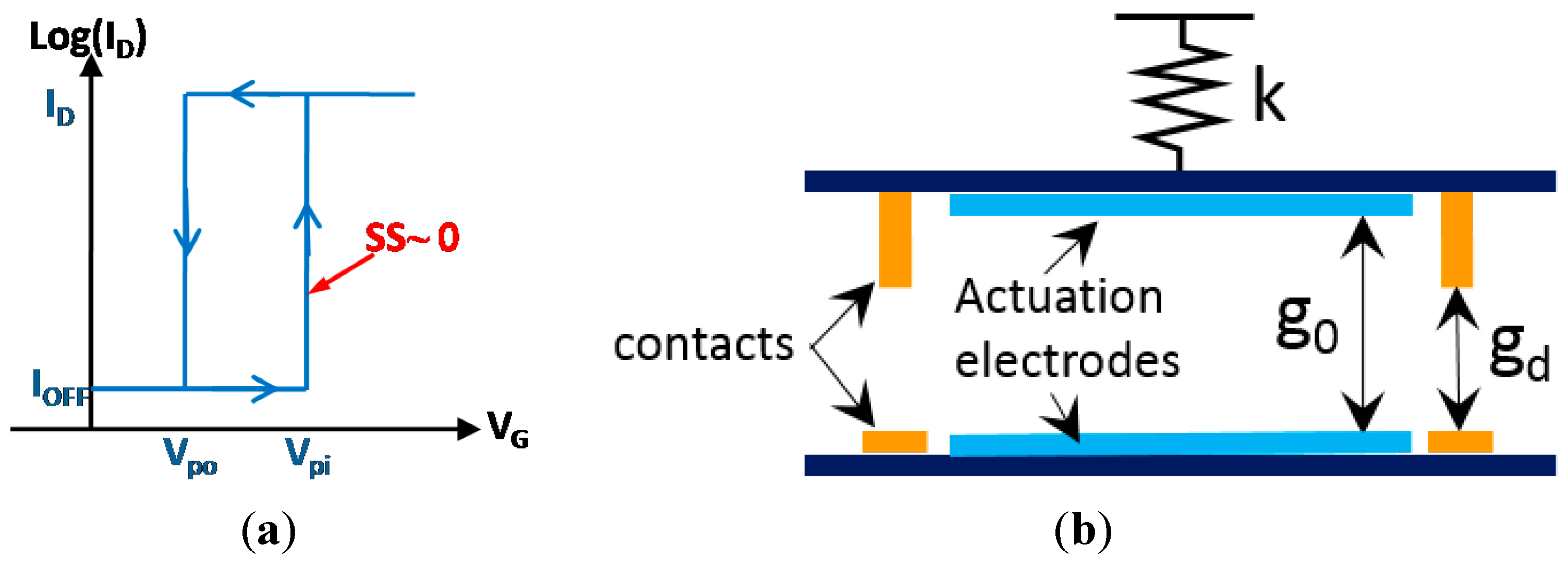
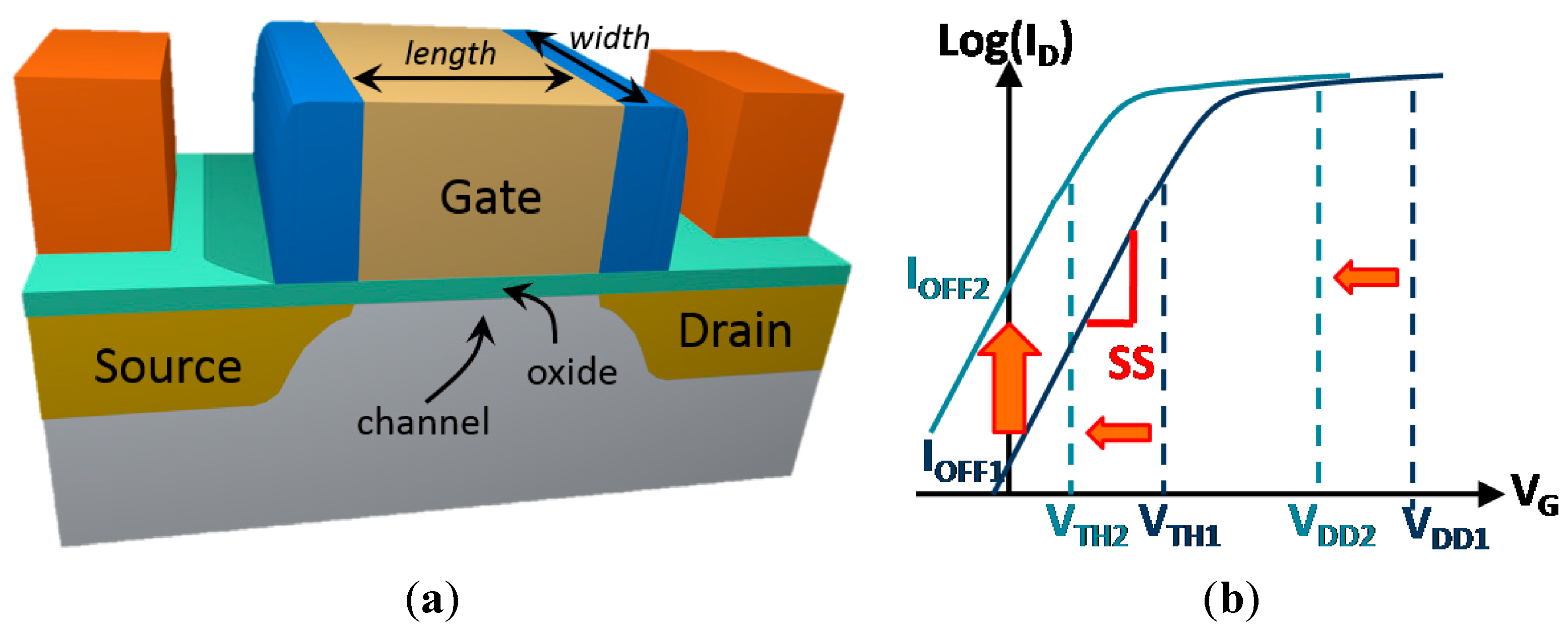
3.2. Device Operation

Figure 4b illustrates the spring model of a NEM relay, which is comprised of a fixed actuation electrode (often defined as the gate, as in a MOSFET) and a movable electrode (often defined as the source in a 3T relay). Physical contact is established between the movable source electrode and a fixed contact electrode (often defined as the drain) in the ON state to allow current to flow and thereby transmit an electrical signal. The state of the relay depends on the forces applied to the movable structure: the electrostatic actuation force (Felec), the mechanical spring force which acts to release the electrode from contact (Frl), and the contact adhesive force (Fadh). As the applied voltage between the actuation electrode and the movable electrode increases, the balance between the electrostatic force and the release force reaches a metastable limit when the distance between them is reduced by g0/3, where g0 is the initial thickness of the air-gap between the actuation and movable electrodes. This point defines the “pull-in” voltage (Vpi). Once the applied voltage is greater than Vpi, the source “snaps” into contact with the drain and the relay is thereby switched ON. Note that the initial thickness of the air-gap between the source and drain electrodes (gd) is smaller than g0 to avoid ensure zero gate current. Similarly, the balance between the electrostatic force, the release force, and the adhesion force just before contact is broken defines the “pull-out” voltage (Vpo), which is sometimes also referred to as the release voltage. When the applied voltage becomes lower than the “pull-out” voltage (Vpo), the source electrode is actuated out of contact so that current can no longer flow. The “pull-in” and “pull-out” voltages are given by the following equations:
V p i =   8 k g 0 3 27 ε 0 L w
V p o = 2 ( g 0 g d ) 2 ε 0 L w ( k g d F a d h )
where k is the effective spring constant (stiffness) of the movable electrode, ε0 is the dielectric permittivity of air, and L and w are the length and the width of the actuation electrode, respectively. (These equations are valid for a “pull-in mode” relay, that is if gd/g0 > 1/3. If gd/g0 < 1/3, then contact is made before the pull-in point and the relay is said to be operating in “non-pull-in” mode.) It should be noted that Equation (1) assumes quasi-static operation. In dynamic operation, the kinetic energy of the movable electrode tends to decrease the value of the pull-in voltage: For a step actuation voltage, the dynamic value of the pull-in voltage can be analytically calculated and is equal to 91.9% of the value calculated by Equation (1) for the case of no damping [25].

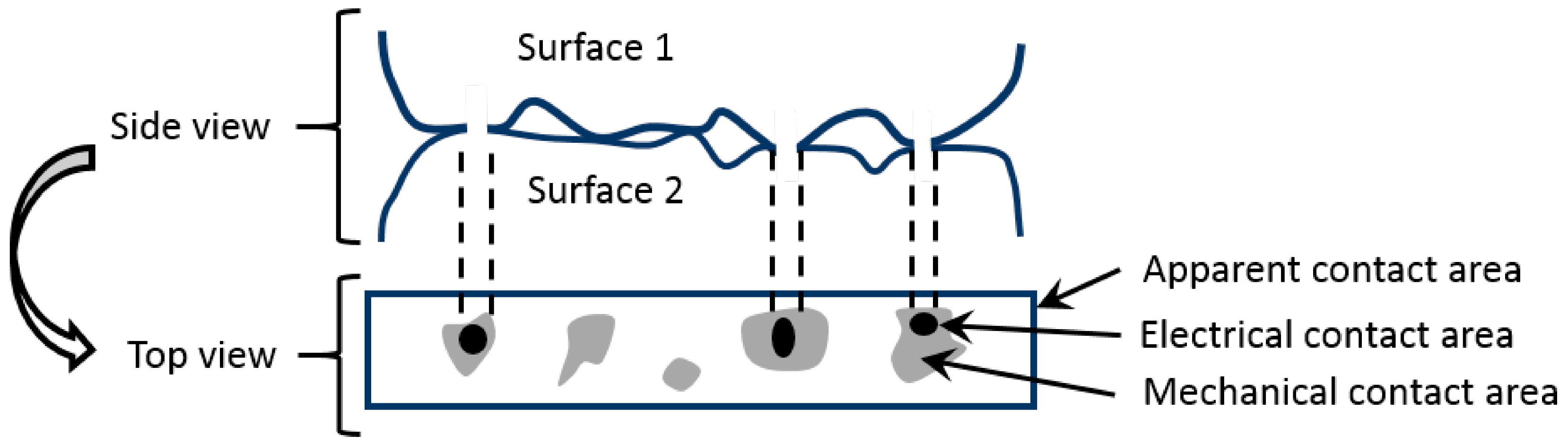
3.3. Contact Resistance

The primary measure of the quality of an electrical contact is the contact resistance Rc. The notion of contact resistance is not as trivial as it may first appear. It involves the physics of contact mechanics with electrical conduction. The first model was developed by Holm in 1967 [26] and numerous works have been conducted since then to describe contact physics according to geometry (sphere, flat), material (elastic, plastic), surface roughness, adhesion, etc. [27]. A recent review summarized the different models and works in this regard [28]. Due to roughness of the contacting surfaces, only some small parts within the apparent contact area are in physical contact when the relay is in the ON state; these correspond to the points of the highest asperities (Figure 5). Some of those contact points might not be conductive, however. The sum of currents flowing through the conductive contacting points determines the contact resistance. In a NEM relay, the contact resistance is given by the Sharvin model, due to the small dimensions of the contact. Rc depends on the electrical resistivity ρ, the electron mean free path l, and the radius of the contacting asperity r:
R c = R S h =   4 ρ l 3 π r 2
In contrast to RF MEM relays for which the contact resistance should be lower than 1 Ω to achieve low insertion loss, a NEM relay can have contact resistance as high as several kΩ because the digital circuit operating speed is limited by the mechanical switching delay of the relay rather than the electrical (“RC”) charging delay. This tolerance for high Rc allows for more possibilities to find a high endurance contact material.
Figure 5. Illustration of the apparent, mechanical, and electrical contact areas.
Micromachines 06 01046 g005

4. Recent Progress in Electrostatic M/NEM Logic Relay Technology

This section highlights recent work by various research groups that are investigating NEM relays for digital logic applications.

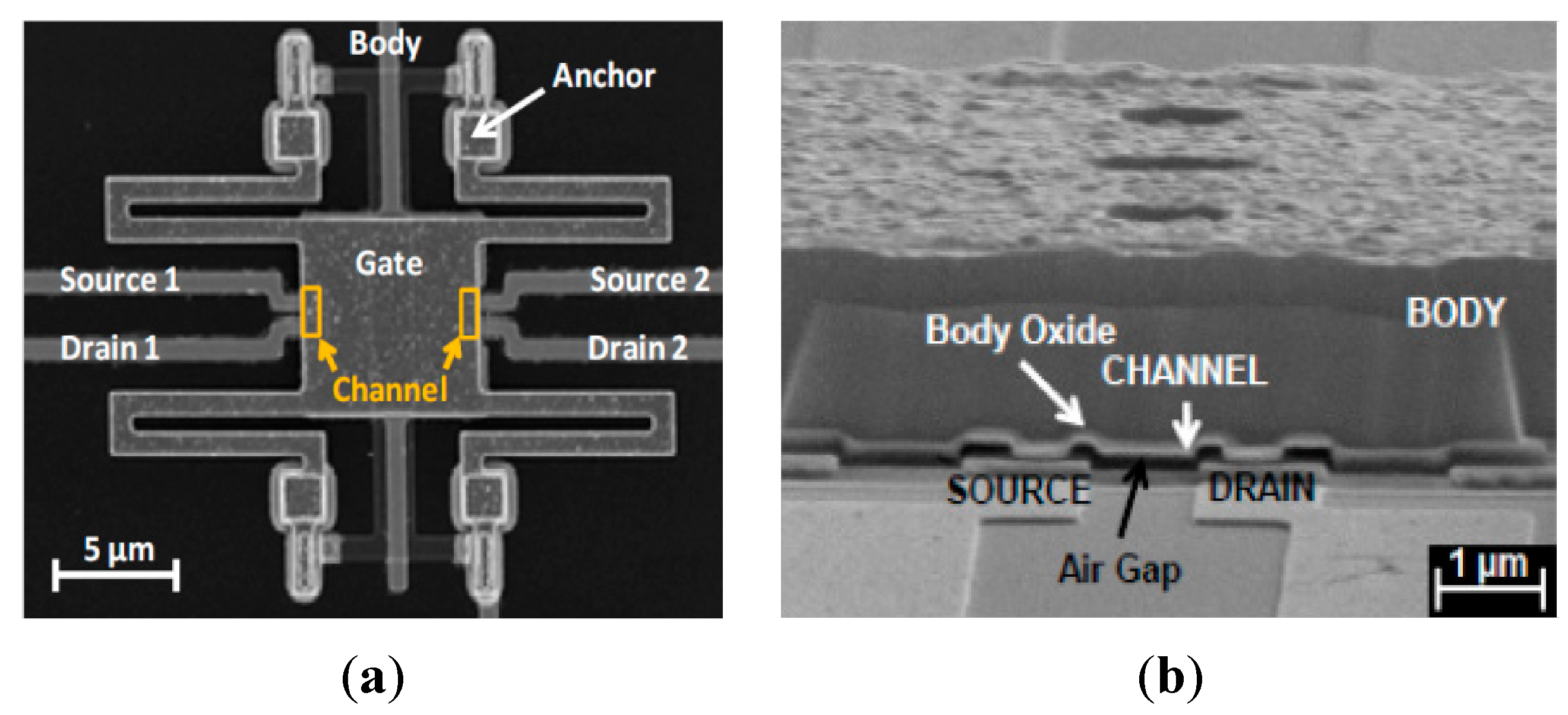
4.1. First Demonstration of a NEM Relay

The article of Jang et al. [29] in 2005 is one of the earliest demonstrations of a NEM relay following the work of Rueckes et al. [30]. This relay is comprised of three multi-walled carbon nanotubes (MWCNT) whose vertical orientation facilitates higher device integration density. The source and drain CNT electrodes are on the left, whereas the gate CNT electrode is on the right (Figure 6a). By applying a positive voltage to each of the drain and gate electrodes, the drain CNT bends towards the grounded source to establish physical contact. In this first publication, the actuation voltage applied to the gate is around 24 V. A second publication by the same team in 2008 showed a more optimal placement of the gate electrode, at around 30 nm from the CNT drain. This improved design resulted in lower actuation voltage, around 4.5 V [31].
Within the last 10 years, several NEM relays based on CNT [32], graphene, or nanowires have been fabricated [33]. They offer attractive performance characteristics: a high on/off current ratio (ION/IOFF), a high switching speed (approximately 1 ns), and a pull-in voltage that can reach down to a few volts [34,35]. Each of these devices was fabricated using a “bottom-up” approach, which presents challenges for high-volume manufacturing. Manual tools are sometimes needed to manipulate the wires to create the relays [30], however. Another practical challenge for implementing relays with CNTs is a significant decrease (by multiple orders of magnitude) in the conductivity of a metallic CNT upon mechanical bending [36,37]. Additional issues are a relatively large actuation voltage (inherent due to the small actuation area), a large hysteresis voltage [38], and low endurance. A large number of those works have been summarized in the review of Loh and Espinosa [39]. Below, we mainly consider NEM relays fabricated with conventional “top-down” fabrication processes which are more suitable for co-integration with CMOS transistors.

4.2. First Demonstration of a NEM Relay Using a CMOS-Compatible “Top-Down” Fabrication Process

The first demonstration of an electrostatically actuated mechanical switch with nanometer-scale dimensions fabricated using a top-down process was published by Jang et al.; however, it is a two-terminal device [40,41], not suitable for logic applications. A nanoscale 3T relay from the same research team was reported soon afterwards (Figure 6b) [42]: the length of the beam is 700 nm and the as-fabricated contact gap thickness is 40 nm. The contact material is TiN. This relay was immersed in a liquid medium (oil) to reduce its pull-in voltage. The pull-in voltage varies substantially from 8 V to 12 V in air and from 4 V to 8 V in oil. The endurance is only a few cycles, both in air and oil (VDD = 5 V, ID = 10 nA). Another 2T device was presented in 2013 with a “pipe-clip” structure, with a minimum contact gap thickness of only 4 nm (the smallest to date) [43].
Figure 6. (a) First demonstration of NEM relay using MWCNT [29] (Reprinted with permission from [29], copyright 2005, AIP Publishing LLC). (b) Demonstration of “top-down” fabricated 3T relay developed in KAIST [42] (© 2009 IEEE, reprinted with permission from [42]).
Micromachines 06 01046 g006

4.3. Other Relays Fabricated Using CMOS-Compatible Processes

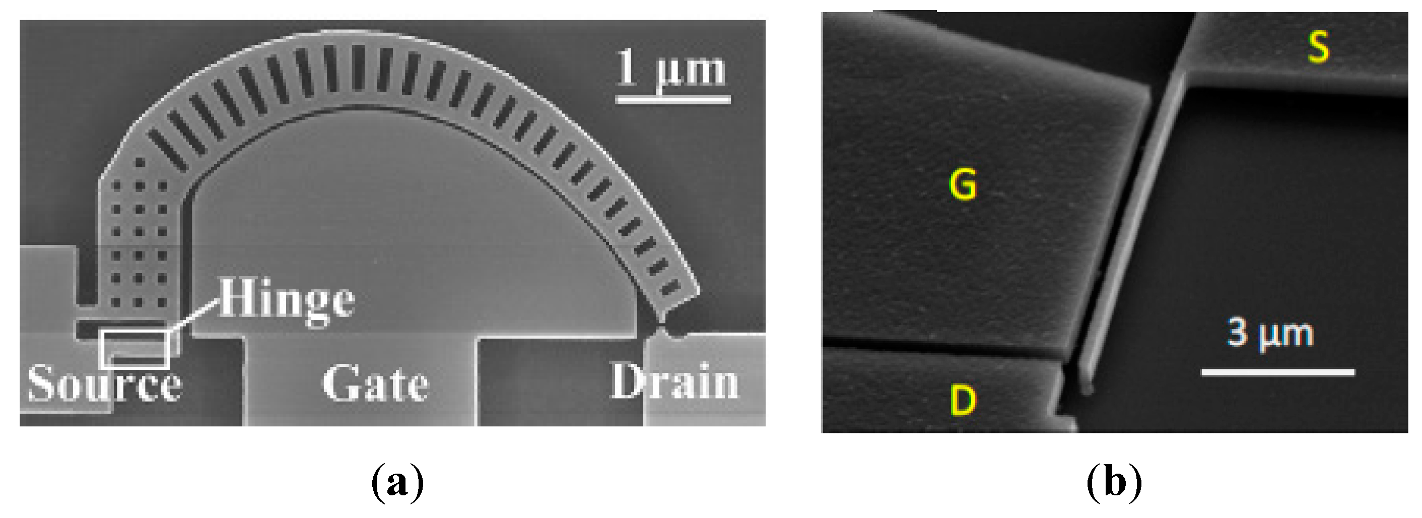
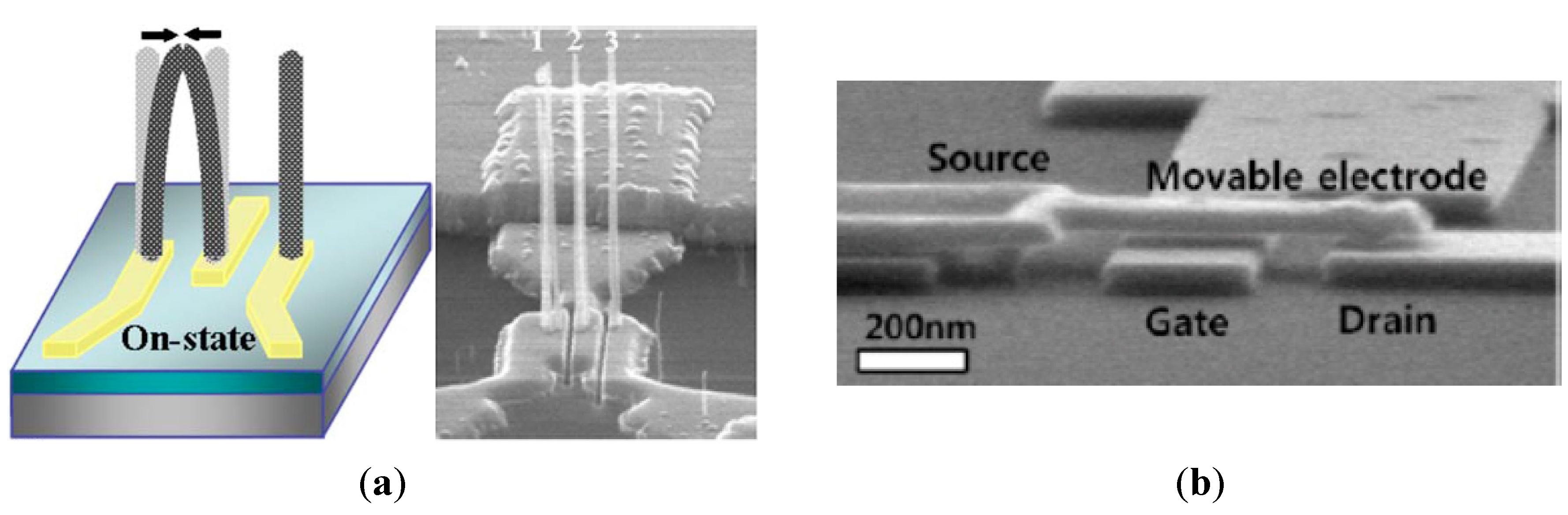
4.3.1. “Out-of-Plane” Actuation Relays

The logic relay developed at UC Berkeley is comprised of a movable body electrode formed in a layer of polycrystalline silicon-germanium to which a conductive strip of metal (the “channel”) is attached via an insulating layer of aluminum-oxide (Figure 7) [44,45,46]. Two variations of this insulated-body relay design, 4T and 6T, have been reported. The contacting electrode material initially was tungsten (W) and later changed to ruthenium (Ru) and other materials for improved Rc stability [47,48]. Although the in-plane dimensions of this relay are in the micrometer range, the as-fabricated contact gap thickness (gd) is in the nanoscale range [44]. Operating (gate voltage) lower than 1 V has been enabled by applying a body bias voltage [48] with a turn-on delay below 1 µs. Reliability studies have shown that Rc remains below 10 kΩ under hot switching conditions for more than 108 cycles [49]. Circuits designed with such devices are expected to operate with at least one order of magnitude better energy efficiency than their CMOS counterparts, based on a benchmarking study of 32-bit adder performance at the 65 nm technology node [22,50].
Figure 7. Scanning electron micrographs of a logic relay fabricated by researchers at the University of California, Berkeley: (a) Plan view of a 6T relay [46] (© 2012 IEEE, reprinted with permission from [46]). (b) Tilted cross-sectional view of the relay along the channel, source, and drain of the relay.
Micromachines 06 01046 g007

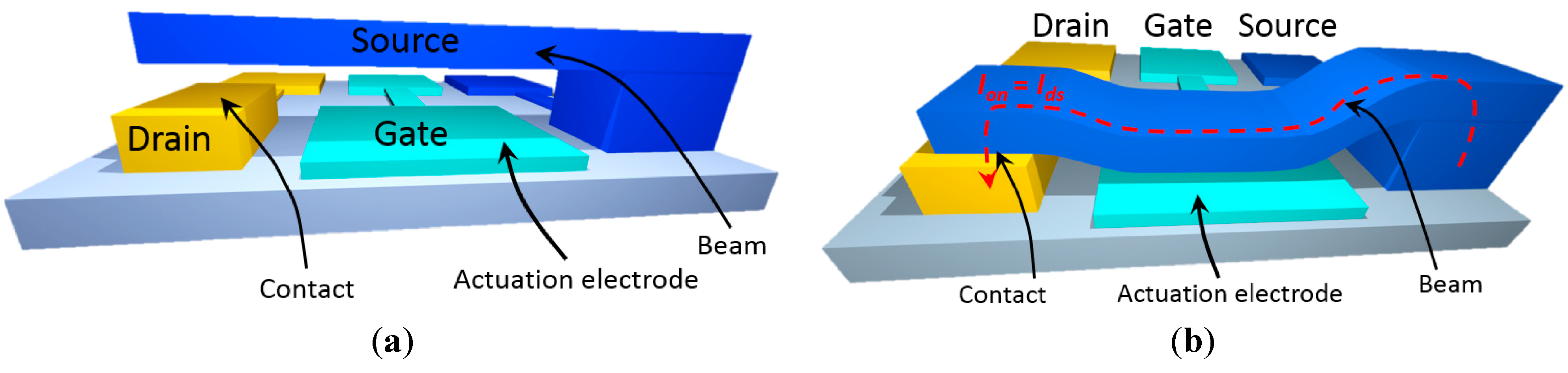
4.3.2. “In-Plane” Actuation Relays

The first relay publication from the research group at Stanford University concerned the design and prospects of NEM relays for logic applications [16,51]. It notes that low-density structural materials (Si or Al) and the presence of a contact “bump” (to reduce the as-fabricated contact gap thickness) can provide switching times to be on the order of nanoseconds. Although logic gates implemented with NEM relays still would operate more slowly (sub-GHz) than logic gates implemented with CMOS transistors, they could have lower energy loss for equivalent areas (Estat < 0.1 fJ for A < 0.03 μm2).
Two subsequent articles published by the same group at Stanford mainly focused on device fabrication. The first one [52] shows the design and the fabrication process for a planar laterally actuated poly-Si relay with Pt as the contact electrode material. Two proof-of-concept devices, simple cantilever or double-clamped beam structures, were reported with actuation voltage Vact > 12.5 V (Vpo > 3 V) and Vact > 26 V (Vpo > 19 V). The second article [53] goes further by detailing the properties and applications of NEM relays, the advantages of lateral actuation, device simulations, fabrication process development, reliability testing, and the demonstration of a relay multiplexer. The results show improved performance with Vact =10.7 V (Vpi =7.9 V), Rc ≈ 3 kΩ with Pt contact coating. Cycling tests under “hot switching” conditions (1 V/1 µA) demonstrated endurance greater than 108 cycles.
Recently, European researchers in Switzerland and the United Kingdom (IBM, EPFL, University of Bristol, TEC) have made 3T and 4T NEM relays with an in-plane curved cantilever structure (Figure 8a) [54,55]. Among the physical dimensions are an as-fabricated contact gap thickness of 50 nm and a total surface area estimated to 15 µm2. An amorphous carbon coating layer (a-C) reduces the contact resistance to Rc = 15 kΩ and reduces the hysteresis voltage to 0.5 V, four times lower than for Pt contacts [56]. The pull-in and pull-out voltage are about 7 V and 5 V, respectively. Actuation with ±0.5 V swing has been achieved by applying a bias voltage [57]. The turn-on delay is about 200 ns.

4.3.3. Silicon Carbide (SiC) Relays for Harsh Environments

The robust properties of SiC at high temperatures make this material attractive for outer space and military applications. Various NEM relays using SiC nanowires were fabricated using a top-down approach by a research group at Case Western Reserve University in collaboration with researchers at the California Institute of Technology. They fabricated 2T switches using a very thin beam [58] and, more recently, 3T relays were fabricated [59,60] with a footprint of 1 µm2 and an as-fabricated contact air-gap thickness of 100 nm (Figure 8b). Electrical characterizations of the relay operating at room temperature and at 500 °C demonstrated switching voltages of 15 V and 11 V, respectively. The endurance of this device is better than 14,000 cycles under “hot-switching” conditions (100 mV/150 nA) at 0.125 Hz. Several logic gates (AND, XOR) based on this relay technology were also demonstrated [61,62,63].
Figure 8. (a) NEM relay with a curved cantilever [57] (© 2014 IEEE, reprinted with permission from [57]). (b) SiC relay [59] (© 2013 IEEE, reprinted with permission from [59]).
Micromachines 06 01046 g008

4.4. Additional NEM Switch Demonstrations

A research team from Sandia National Laboratories also developed a laterally actuated NEM relay [64]. Numerous switches with very small dimensions of actuation gap thickness (30–100 nm) and contact gap thickness (20–70 nm) were fabricated, but only a few were able to be actuated due to a low manufacturing process yield. Their pull-in voltages are higher than 4 V with a turn-on delay of a few hundred ns. Endurance testing at 1 kHz demonstrated more than 2 × 10⁶ cycles.
Researchers at Cornell University demonstrated a vertically oriented, laterally actuated 4T NEM relay [65]. The channel electrode is mounted on a Si pillar whose thickness is around 150 nm. The initial distance between the two contacting electrodes (metal material not specified) is estimated to be between 200 nm and 350 nm. Contact is made by bending and torsion of the pillar. However, after the first actuation, only the torsional mode is available, as the channel is definitively stuck to the drain. The pull-in voltage is 15 V for the first actuation and 10 V for subsequent cycles.
A team from the National University of Singapore has made a NEM relay with two torsion bars for a non-volatile memory application [66]. The footprint of the device is in the micrometer range (L = 9 µm, W = 1 µm) and the as-fabricated contact gap thickness is between 80 nm and 100 nm. The pull-in voltage is Vpi = 5.5 V. The cycling tests do not show promising results, as the relay demonstrates unstable behavior after only a few cycles.

4.5. Summary

Table 1 summarizes key features of the aforementioned NEM relays. The first two rows list devices fabricated with bottom-up processes, but they are included since they were the first demonstrations of NEM relays.
Table 1. Summary of reported nano-electro-mechanical (NEM) relays for logic applications (Areas in parentheses are estimated).
Research GroupTypeAreac-gapVpiRcCyclesMaterialCircuit
First CNT [29,31]3T-30 nm4.5 V1 MΩ>1CNTNo
First Top-Down (KAIST) [40,41,42,43]3T-40 nm4 V->10TiNNo
Out-of-Plane (UC Berkeley) [44,45,46,47,48,49,50]4T 6T-80 nm<1 V1 kΩ>108W RuYes
6T-250 nm10 V->1TiO2Yes
In-Plane (Stanford University) [51,52,53]5T--7.9 V3 kΩ108PtYes
Curved (NEMIAC) [54,55,56,57]3T 4T15 µm250 nm0.5 V5 kΩ>108a-CYes
SiC Relays (CWR University) [58,59,60,61,62,63]3T1 µm2100 nm15 V10 MΩ>14,000SiCYes
Sandia National Lab [64]3T(10 µm2)30 nm>4 V-2 × 10⁶RuNo
Cornell University [65]3T(3 µm2)200 nm10 V10 MΩ--No
Piezoelectric (CM University) [21,22,23]4T58 µm2-10 mV16 kΩ-PtNo

5. Relay-Based Logic Circuit Design

Simple relay-based logic gates (AND, XOR, etc.) have been demonstrated in [58,59,60]. Since the mechanical switching delay (greater than 1 ns) of a relay is orders of magnitude larger than its electrical charging/discharging delay (less than 1 ps for Rc on the order of kΩ), very-large-scale integrated (VLSI) relay circuits should be comprised of single-stage complex logic gates, so that the delay per operation is essentially one mechanical delay [17]. Relay-based ICs following this design methodology were demonstrated in [50].
Since the optimal topology of a relay-based circuit is quite different than a CMOS implementation, a fair comparison of relay vs. CMOS energy performance must be made at the circuit (block) level rather than at the device level. Although digital systems comprise a variety of functional blocks, the energy performance tradeoffs for the majority of CMOS gates are similar to that of a CMOS inverter. Therefore, a representative comparison can be made for a relay chain vs. a CMOS inverter chain, as shown in Figure 9. Simulation-based studies project NEM relay technology to be able to achieve more than a one order of magnitude improvement in energy efficiency as compared with CMOS technology, for an equivalent area and a mechanical switching delay of 10 ns [17,50].
Figure 9. Illustration of digital signal propagation delay in optimally designed (a) complementary metal-oxide-semiconductor (CMOS) logic circuit, (b) NEM relay-based logic circuit.
Micromachines 06 01046 g009
Hybrid CMOS/NEM technology can potentially achieve the advantages of high-speed CMOS operation together with low-power NEM relay operation [67]. For example, a hybrid NEMS/CMOS static random-access memory (SRAM) cell design for lower static power dissipation and improved cell stability is proposed in [48], and projected to provide a reduction in energy loss of 85%, improvement in write and read times by 60% and 10%, respectively, and an improved static noise margin. As another example, NEM relays can be monolithically integrated with CMOS devices to implement non-volatile SRAM and non-volatile content-addressable memory (CAM) for reduced power consumption [68].

6. Remaining Challenges and Pathways to Solutions for NEM Relay Technology

Although MEM relays for RF signal switching have been investigated for several decades, NEM relays for digital logic applications have drawn increasing attention only recently. The works reviewed in the last two sections (even if not exhaustive) are a good indicator: 72% of the referenced articles appeared within the last five years and 50% within the last three years. Further work is needed to address the following remaining challenges and for NEM relays to be practical for low-power digital computing:
  • The ability to achieve high manufacturing yield. This is especially a challenge for NEM relays incorporating carbon nanotubes, nanowires, or graphene, which are fabricated using bottom-up processes. Well-established top-down planar processing and surface-micromachining techniques should be leveraged for the high-volume manufacture of NEM relays. Ideally, a relay fabrication process should be compatible with back-end-of-line (BEOL) processing to facilitate co-integration with CMOS circuitry [69].
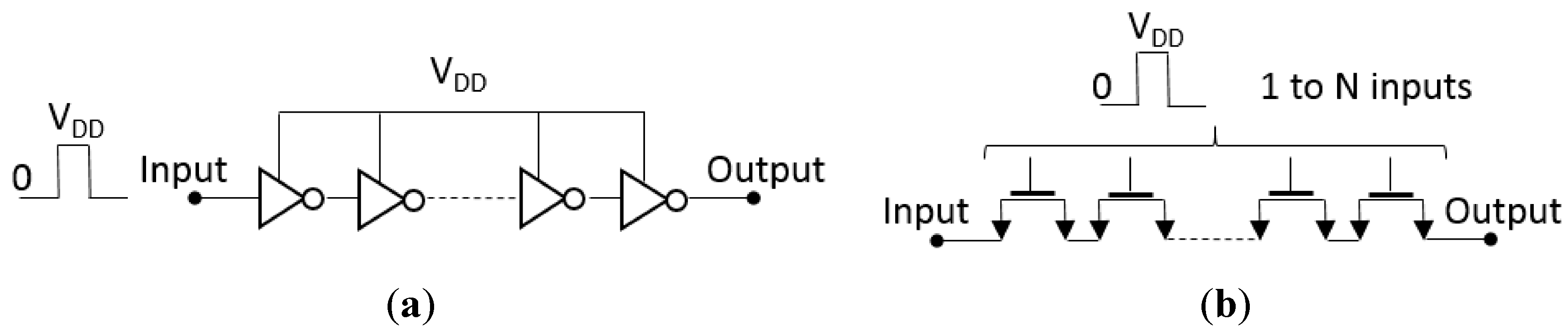
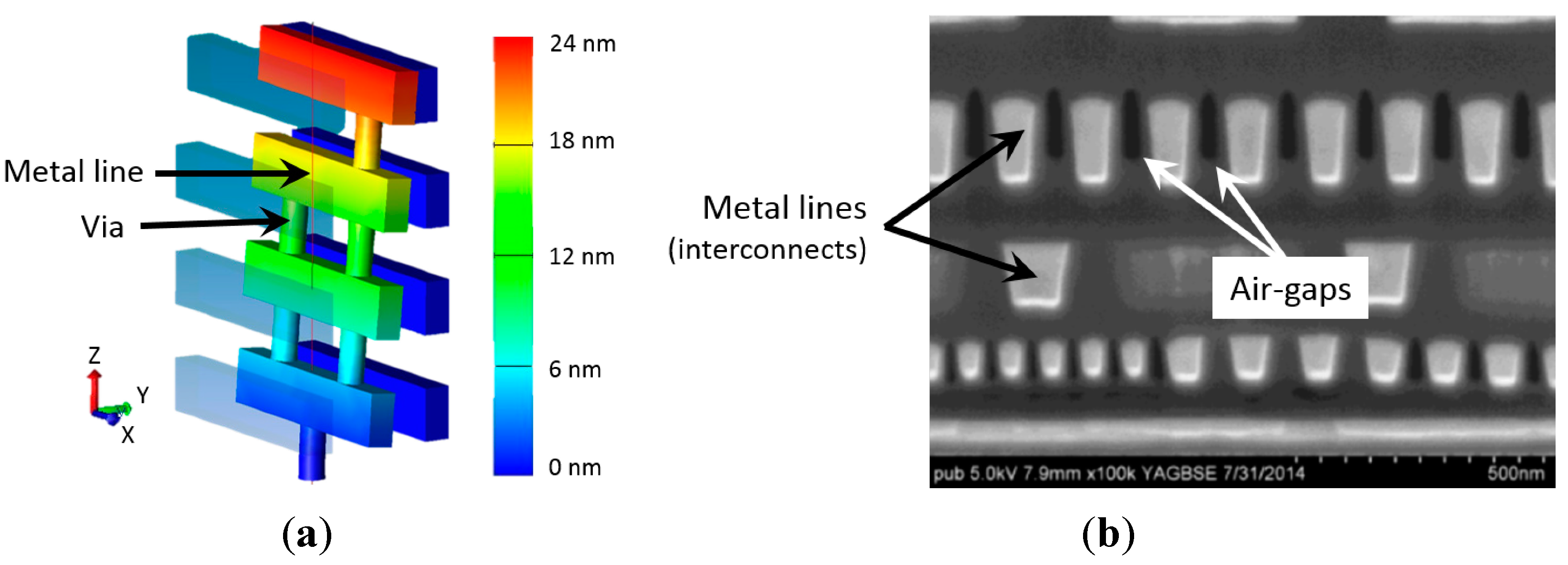
  • The ability to scale down the device footprint. Most of the NEM relays reported to date have micrometer-scale lateral dimensions. Reducing the size of the relay is particularly constrained by the requirement of low actuation voltage and the fact that the contact air-gap thickness cannot be infinitesimally small. A large area is needed to generate a large enough Felec to overcome Frl, which in turn has to be larger than Fadh [70]. To reduce the footprint of a NEM relay to below 0.1 µm2, researchers at the University of California, Berkeley, have proposed to utilize multiple layers of metal to implement a compact, vertically oriented structure (Figure 10a) [68]. This design is based on the utilization of several layers of air-gap interconnects available in state-of-the-art CMOS technology (Figure 10b) [71], and can achieve a very low pull-in voltage (Vpi = 1 V for A < 0.1 µm2 and 20 ns switching delay). The feasibility of this approach remains to be proven.
  • The ability to operate at a very low voltage for low active power consumption. Minimization of adhesion at contacting asperities is a challenge for achieving a very low (mV) operating voltage, since Felec decreases quadratically with decreasing actuation voltage and must be greater than Fadh. This sets the fundamental energy efficiency limit for a relay. Adhesion is not fully understood in electrical contacts. However, numerous studies of mechanical contact have emerged in recent years, especially to meet the need in microsystems [72,73].
    It should be noted that the actuation area and/or the operating voltage of a 4T relay can be reduced by applying a body bias voltage to reduce the gate voltage swing required to operate the switch. The hysteresis voltage limits the degree to which the gate voltage swing can be reduced in this manner, however, pointing again to the need to minimize contact adhesive force. Several NEM relays have already demonstrated sub-1 V operating voltages using the body-biasing technique [22,48,54].
  • The ability to achieve sufficiently high endurance. An endurance of 3 × 10¹⁴ (i.e., less than one quadrillion) ON/OFF switching cycles is sufficient to guarantee device functionality over a period of 10 years at 100 MHz operating frequency with a duty factor of 1%. To date, the best NEM relay endurance demonstrated is less than 1010 cycles. Relay failure modes are well known, as they are similar to those observed for RF MEMS relays: either oxidation of the contact surfaces, which induces a strong increase of the contact resistance at low contact voltages, or material transfer, which results in stiction (welding) [74,75]. Of these two failure modes, it appears that oxidation of the contact surfaces is the main limiting one for logic relays. Indeed, in [76], a reliability model is developed to project the number of switching cycles before welding-induced failure as a function of 1/V, and accelerated lifetime tests indicate that endurance should exceed 1014 cycles for operating voltages below 1 V; the projected endurance goes up to 1016 cycles at 0.5 V. Therefore, contact welding is not anticipated to be the main reliability issue for NEM relays.
Figure 10. (a) New vertical NEM relay structure using BEOL metal layers (adapted from [68]). (b) The most advanced BEOL technology incorporates air-gaps between metal interconnects [71] (© 2014 IEEE, reprinted with permission from [71]).
Micromachines 06 01046 g010
Contact material selection is key to overcoming the reliability challenge for NEM relays. A larger range of materials can be considered for NEM relays than for RF MEM switches since low contact resistance is not required. The main difficulty is to find a material that is mechanically durable and electrically stable over 1015 switching cycles. Several works have helped to narrow down the material choices. The article of Chowdhury et al. [77] deals with the study of contact materials with an atomic force microscope (AFM)-based experiment. The study is performed using a Cr AFM cantilever to make/break contact with several substrate materials (Ir, Pt, W, Ni, Cr, Ti, Cu, Al, and graphite). Best results are obtained with Ti contacts, which show good cycling behavior with relatively low adhesion and low contact resistance (attributed to the rupture of the native Ti oxide) over 105 cycles. Graphite also shows good results with cycles with a low adhesive force (65 nN) and stable contact resistance. W and Pt have the lowest adhesive forces (<25 nN) but their contact resistances increase over time [49]. Contact oxidation in addition to high adhesion force (>100 nN) is also observed for Al, Ir, and Cu. Cr and Ni have intermediate results as their values of adhesion forces are 62 nN and 65 nN, respectively. Their contact resistances are stable but typically very high (100 to 1000 times higher than other materials). Gold (Au) does not appear to be an appropriate material because of its low hardness. Amorphous carbon has been used in some relays and shows low adhesion (<100 nN) and good Rc (15 kΩ) over 108 cycles, which makes it a potential candidate for contacts in NEM relays [56].
A promising contact material appears to be Ru and/or its oxide RuO2. Indeed, recent studies performed by Czaplewski et al. [78] showed that RuO2 (over Au) contacts could reach more than 1010 cycles in MEM relays without failure. Such a performance was obtained by optimizing the design to reduce the impact velocity and, thus, the plastic deformation to the contact, and by using an inorganic sacrificial layer during the fabrication steps. Ruthenium oxide is an electrically conductive material whose electrical resistivity is only seven times higher than that of ruthenium. Therefore, thanks to its electrical conductivity and its resistance to oxidization (as it is a stable oxide), RuO2 appears to be an intriguing contact material for NEM relays.

7. Conclusions

The fundamental limitation in the energy efficiency of CMOS digital logic circuits necessitates new logic switch technology to enable continued improvement in chip functionality within power density constraints. NEM relays are promising candidates for low-power applications as they have negligible OFF-state leakage current (IOFF) and abrupt switching behavior which, in principle, enables very low switching voltages. Much progress has been made in recent years (Table 1) toward realizing this promise. Further work is needed to develop compact NEM relays that can be manufactured with high device yield and that can be operated with a very low voltage with sufficient reliability (contact resistance stability) to have a revolutionary impact for future IC technology.

Acknowledgments

This work was supported in part by NSF Award 0939514. Alexis Peschot gratefully acknowledges post-doctoral fellowship support from the DGA (Delegation Generale de l’Armement).

Conflicts of Interest

The authors declare no conflict of interest.

References

  1. Moore, G.E. Cramming more components onto integrated circuits. Electronics 1965, 38, 114–117. [Google Scholar]
  2. International Technology Roadmap for Semiconductors, 2008 Edition. Available online: http://www.itrs.net/ (accessed on 5 August 2015).
  3. Haensch, W.; Nowak, E.J.; Dennard, R.H.; Solomon, P.M.; Bryant, A.; Dokumaci, O.H.; Kumar, A.; Wang, X.; Johnson, J.B.; Fischetti, M.V. Silicon CMOS devices beyond scaling. IBM J. Res. Dev. 2006, 50, 339–361. [Google Scholar] [CrossRef]
  4. Taylor, M.B. Is dark silicon useful? Harnessing the four horsemen of the coming dark silicon apocalypse. In Proceedings of the 49th Annual Design Automation Conference, San Francisco, CA, USA, 3–7 June 2012; pp. 1131–1136.
  5. Thompson, S.E.; Armstrong, M.; Auth, C.; Alavi, M.; Buehler, M.; Chau, R.; Cea, S.; Ghani, T.; Glass, G.; Hoffman, T.; et al. A 90-nm logic technology featuring strained-silicon. IEEE Trans. Electron Devices 2004, 51, 1790–1797. [Google Scholar] [CrossRef]
  6. Mistry, K.; Allen, C.; Auth, C.; Beattie, B.; Bergstrom, D.; Bost, M.; Brazier, M.; Buehler, M.; Cappellani, A.; Chau, R.; et al. A 45nm logic technology with high-k plus metal gate transistors, strained silicon, 9 Cu interconnect layers, 193 nm dry patterning, and 100% Pb-free packaging. In Proceedings of the IEEE International Electron Devices Meeting, Washington, DC, USA, 10–12 December 2007; pp. 247–250.
  7. Cheng, K.; Khakifirooz, A.; Kulkarni, P.; Ponoth, S.; Haran, B.; Kumar, A.; Adam, T.; Reznicek, A.; Loubet, N.; He, H.; et al. ETSOI CMOS for system-on-chip applications featuring 22 nm gate length, sub-100 nm gate pitch, and 0.08 µm2 SRAM cell. In Proceedings of 2011 Symposium on VLSI Technology, Honolulu, HI, USA, 14–16 June 2011; pp. 128–129.
  8. Hisamoto, D.; Lee, W.C.; Kedzierski, J.; Takeuchi, H.; Asano, K.; Kuo, C.; Anderson, E.; King, T.J.; Bokor, J.; Hu, C. FinFET—A self-aligned double-gate MOSFET scalable to 20 nm. IEEE Trans Electron Devices 2000, 47, 2320–2325. [Google Scholar]
  9. Auth, C.; Allen, C.; Blattner, A.; Bergstrom, D.; Brazier, M.; Bost, M.; Buehler, M.; Chikarmane, V.; Ghani, T.; Glassman, T.; et al. A 22nm high performance and low-power CMOS technology featuring fully-depleted tri-gate transistors, self-aligned contacts and high density MIM capacitors. In Proceedings of 2012 Symposium on VLSI Technology, Honolulu, HI, USA, 12–14 June 2012; pp. 131–132.
  10. Knoch, J.; Appenzeller, J. A novel concept for field-effect transistors-the tunneling carbon nanotube FET. In Proceedings of 63rd Device Research Conference Digest (DRC 05), Santa Barbara, CA, USA, 20–22 June 2005; pp. 153–156.
  11. Seabaugh, A.C.; Zhang, Q. Low-voltage tunnel transistors for beyond CMOS logic. Proc. IEEE 2010, 98, 2095–2110. [Google Scholar] [CrossRef]
  12. Choi, W.Y.; Park, B.G.; Lee, J.D.; Liu, T.-J.K. Tunneling field-effect transistors (TFETs) with subthreshold swing (SS) less than 60 mV/dec. IEEE Electron Device Lett. 2007, 28, 743–745. [Google Scholar] [CrossRef]
  13. Kim, S.H.; Kam, H.; Hu, C.; Liu, T.-J.K. Germanium-source tunnel field effect transistors with record high ION/IOFF. In Proceedings of 2009 Symposium on VLSI Technology, Honolulu, HI, USA, 16–18 June 2009; pp. 178–179.
  14. White, S. A Brief History of Computing. Available online: http://trillian.randomstuff.org.uk/~stephen/history/ (accessed on 6 August 2015).
  15. Bustillo, J.M.; Howe, R.T.; Muller, R.S. Surface micromachining for microelectromechanical systems. Proc. IEEE 1998, 86, 1552–1574. [Google Scholar] [CrossRef]
  16. Akarvardar, K.; Elata, D.; Parsa, R.; Wan, G.C.; Yoo, K.; Provine, J.; Peumans, P.; Howe, R.T.; Wong, H.S.P. Design considerations for complementary nanoelectromechanical logic gates. In Proceedings of IEEE International Electron Devices Meeting (IEDM 2007), Washington, DC, USA, 10–12 December 2007; pp. 299–302.
  17. Chen, F.; Kam, H.; Marković, D.; Liu, T.-J.K.; Stojanović, V.; Alon, E. Integrated circuit design with NEM relays. In Proceedings of the IEEE/ACM International Conference on Computer-Aided Design, San Jose, CA, USA, November 2008; pp. 750–757.
  18. Petersen, K.E. Micromechanical membrane switches on silicon. IBM J. Res. Dev. 1979, 23, 376–385. [Google Scholar] [CrossRef]
  19. Rebeiz, G.M. RF MEMS: Theory, Design, and Technology; Wiley: Hoboken, NJ, USA, 2003. [Google Scholar]
  20. Rebeiz, G.M.; Patel, C.D.; Han, S.K.; Ko, C.H.; Ho, K.M.J. The search for a reliable MEMS switch? IEEE Microw. Mag. 2013, 14, 57–67. [Google Scholar] [CrossRef]
  21. Zaghloul, U.; Piazza, G. 10–25 nm piezoelectric nano-actuators and NEMS switches for millivolt computational logic. In Proceedings of the IEEE International Conference on Micro Electro Mechanical Systems (MEMS), Taipei, Taiwan, 20–24 January 2013; pp. 233–236.
  22. Zaghloul, U.; Piazza, G. Sub-1-volt piezoelectric nanoelectromechanical relays with millivolt switching capability. IEEE Electron Device Lett. 2014, 35, 669–671. [Google Scholar]
  23. Piazza, G. Aluminum nitride piezoelectric NEMS resonators and switches. SPIE Proc. 2010, 7679, 76791L. [Google Scholar]
  24. Qian, C.; Peschot, A.; Chen, I.R.; Chen, Y.H.; Xu, N.; Liu, T.-J.K. Effect of body biasing on the energy-delay performance of logic relays. IEEE Electron Device Lett. 2015, 36, 862–864. [Google Scholar] [CrossRef]
  25. Nielson, G.N.; Barbastathis, G. Dynamic pull-in of parallel-plate and torsional electrostatic MEMS actuators. J. Microelectromech. Syst. 2006, 15, 811–821. [Google Scholar] [CrossRef]
  26. Holm, R. Electric Contacts: Theory and Applications; Springer: Berlin, Germany, 1999. [Google Scholar]
  27. Slade, P.G. Electrical Contacts: Principles and Applications, 2nd ed.; Taylor & Francis: Abingdon, UK, 2013. [Google Scholar]
  28. Toler, B.F.; Coutu, R.A.; McBride, J.W. A review of micro-contact physics for microelectromechanical systems (MEMS) metal contact switches. J. Micromech. Microeng. 2013, 23, 103001. [Google Scholar] [CrossRef]
  29. Jang, J.E.; Cha, S.N.; Choi, Y.; Amaratunga, G.A.J.; Kang, D.J.; Hasko, D.G.; Jung, J.E.; Kim, J.M. Nanoelectromechanical switches with vertically aligned carbon nanotubes. Appl. Phys. Lett. 2005, 87, 163114. [Google Scholar] [CrossRef]
  30. Rueckes, T.; Kim, K.; Joselevich, E.; Tseng, G.Y.; Cheung, C.L.; Lieber, C.M. Carbon nanotube-based nonvolatile random access memory for molecular computing. Science 2000, 289, 94–97. [Google Scholar] [CrossRef] [PubMed]
  31. Jang, J.E.; Cha, S.N.; Choi, Y.; Butler, T.P.; Kang, D.J.; Hasko, D.G.; Jung, J.E.; Jin, Y.W.; Kim, J.M.; Amaratunga, G.A.J. Nanoelectromechanical switch with low voltage drive. Appl. Phys. Lett. 2008, 93, 113105. [Google Scholar] [CrossRef]
  32. Lee, S.W.; Campbell, E.E.B. Nanoelectromechanical devices with carbon nanotubes. Curr. Appl. Phys. 2013, 13, 1844–1859. [Google Scholar] [CrossRef]
  33. Lu, W.; Lieber, C.M. Nanoelectronics from the bottom up. Nat. Mater. 2007, 6, 841–850. [Google Scholar] [CrossRef] [PubMed]
  34. Kaul, A.B.; Wong, E.W.; Epp, L.; Hunt, B.D. Electromechanical carbon nanotube switches for high-frequency applications. Nano Lett. 2006, 6, 942–947. [Google Scholar] [CrossRef] [PubMed]
  35. Cha, S.N.; Jang, J.E.; Choi, Y.; Amaratunga, G.A.J.; Kang, D.J.; Hasko, D.G.; Jung, J.E.; Kim, J.M. Fabrication of a nanoelectromechanical switch using a suspended carbon nanotube. Appl. Phys. Lett. 2005, 86, 083105. [Google Scholar] [CrossRef]
  36. Tombler, T.W.; Zhou, C.W.; Alexseyev, L.; Kong, J.; Dai, H.J.; Lei, L.; Jayanthi, C.S.; Tang, M.J.; Wu, S.Y. Reversible electromechanical characteristics of carbon nanotubes under local-probe manipulation. Nature 2000, 405, 769–772. [Google Scholar] [PubMed]
  37. Farajian, A.A.; Yakobson, B.I.; Mizuseki, H.; Kawazoe, Y. Electronic transport through bent carbon nanotubes: Nanoelectromechanical sensors and switches. Phys. Rev. B 2003, 67, 205423. [Google Scholar] [CrossRef]
  38. Ke, C.H.; Espinosa, H.D. In situ electron microscopy electromechanical characterization of a bistable NEMS device. Small 2006, 2, 1484–1489. [Google Scholar] [CrossRef] [PubMed]
  39. Loh, O.Y.; Espinosa, H.D. Nanoelectromechanical contact switches. Nat. Nanotechnol. 2012, 7, 283–295. [Google Scholar] [CrossRef] [PubMed]
  40. Jang, W.W.; Lee, J.O.; Yoon, J.B.; Kim, M.S.; Lee, J.M.; Kim, S.M.; Cho, K.H.; Kim, D.W.; Park, D.; Lee, W.S. Fabrication and characterization of a nanoelectromechanical switch with 15-nm-thick suspension air gap. Appl. Phys. Lett. 2008, 92, 103110. [Google Scholar] [CrossRef]
  41. Jang, W.W.; Yoon, J.B.; Kim, M.S.; Lee, J.M.; Kim, S.M.; Yoon, E.J.; Cho, K.H.; Lee, S.Y.; Choi, I.H.; Kim, D.W.; et al. NEMS switch with 30 nm-thick beam and 20 nm-thick air-gap for high density non-volatile memory applications. Solid-State Electron. 2008, 52, 1578–1583. [Google Scholar] [CrossRef]
  42. Lee, J.O.; Kim, M.W.; Ko, S.D.; Kang, H.O.; Bae, W.H.; Kang, M.H.; Kim, K.N.; Yoo, D.E.; Yoon, J.B. 3-terminal nanoelectromechanical switching device in insulating liquid media for low voltage operation and reliability improvement. In Proceedings of the IEEE International Electron Devices Meeting Technical Digest, Baltimore, MD, Maryland, 7–9 December 2009; pp. 208–211.
  43. Lee, J.O.; Song, Y.H.; Kim, M.W.; Kang, M.H.; Oh, J.S.; Yang, H.H.; Yoon, J.B. A sub-1-volt nanoelectromechanical switching device. Nat. Nanotechnol. 2013, 8, 36–40. [Google Scholar] [CrossRef] [PubMed]
  44. Nathanael, R.; Pott, V.; Kam, H.; Jeon, J.; Liu, T.-J.K. 4-terminal relay technology for complementary logic. In Proceedings of the IEEE International Electron Devices Meeting Technical Digest, Baltimore, MD, Maryland, 7–9 December 2009; pp. 204–207.
  45. Kam, H.; Pott, V.; Nathanael, R.; Jeon, J.; Alon, E.; Liu, T.-J.K. Design and reliability of a micro-relay technology for zero-standby-power digital logic applications. In Proceedings of the IEEE International Electron Devices Meeting Technical Digest, Baltimore, MD, Maryland, 7–9 December 2009; pp. 757–760.
  46. Liu, T.-J.K.; Hutin, L.; Chen, I.R.; Nathanael, R.; Chen, Y.H.; Spencer, M.; Alon, E. Recent progress and challenges for relay logic switch technology. In Proceedings of 2012 Symposium on VLSI Technology, Honolulu, HI, USA, 12–14 June 2012; pp. 43–44.
  47. Pott, V.; Kam, H.; Nathanael, R.; Jeon, J.; Alon, E.; Liu, T.-J.K. Mechanical computing redux: Relays for integrated circuit applications. Proc. IEEE 2010, 98, 2076–2094. [Google Scholar] [CrossRef]
  48. Chen, I.R.; Hutin, L.; Park, C.; Lee, R.; Nathanael, R.; Yaung, J.; Jeon, J.; Liu, T.-J.K. Scaled micro-relay structure with low strain gradient for reduced operating voltage. ECS Transact. 2012, 45, 101–106. [Google Scholar] [CrossRef]
  49. Chen, Y.H.; Nathanael, R.; Jeon, J.; Yaung, J.; Hutin, L.; Liu, T.-J.K. Characterization of contact resistance stability in MEM relays with tungsten electrodes. J. Microelectromech. Syst. 2012, 21, 511–513. [Google Scholar] [CrossRef]
  50. Spencer, M.; Chen, F.; Wang, C.C.; Nathanael, R.; Fariborzi, H.; Gupta, A.; Kam, H.; Pott, V.; Jeon, J.; Liu, T.-J.K.; et al. Demonstration of integrated micro-electro-mechanical relay circuits for VLSI applications. IEEE J. Solid-State Circuits 2011, 46, 308–320. [Google Scholar] [CrossRef]
  51. Chong, S.; Akarvardar, K.; Parsa, R.; Jun-Bo, Y.; Howe, R.T.; Mitra, S.; Wong, H-S.P. Nanoelectromechanical (NEM) relays integrated with CMOS SRAM for improved stability and low leakage. In Proceedings of the IEEE/ACM International Conference on Computer-Aided Design, San Jose, CA, USA, 2–5 November 2009; pp. 478–484.
  52. Parsa, R.; Shavezipur, M.; Lee, W.S.; Chong, S.; Lee, D.; Wong, H.S.P.; Maboudian, R.; Howe, R.T. Nanoelectromechanical relays with decoupled electrode and suspension. In Proceedings of the 24th IEEE International Conference on Micro Electro Mechanical Systems, Cancun, Mexico, 23–27 January 2011; pp. 1361–1364.
  53. Parsa, R.; Lee, W.S.; Shavezipur, M.; Provine, J.; Maboudian, R.; Mitra, S.; Wong, H.-S.P.; Howe, R.T. Laterally actuated platinum-coated polysilicon NEM relays. J Microelectromech. Syst. 2013, 22, 768–778. [Google Scholar] [CrossRef]
  54. Rana, S.; Qin, T.; Bazigos, A.; Grogg, D.; Despont, M.; Ayala, C.L.; Hagleitner, C.; Ionescu, A.M.; Canegallo, R.; Pamunuwa, D. Energy and latency optimization in NEM relay-based digital circuits. IEEE Trans. Circuits Syst. 2014, 61, 2348–2359. [Google Scholar] [CrossRef]
  55. Bazigos, A.; Ayala, C.L.; Rana, S.; Grogg, D.; Fernandez-Bolanos, M.; Hagleitner, C.; Qin, T.; Pamunuwa, D.; Ionescu, A.M. Electromechanical design space exploration for electrostatically actuated ohmic switches using extended parallel plate compact model. Solid-State Electron. 2014, 99, 93–100. [Google Scholar] [CrossRef]
  56. Grogg, D.; Ayala, C.L.; Drechsler, U.; Sebastian, A.; Koelmans, W.W.; Bleiker, S.J.; Fernandez-Bolanos, M.; Hagleitner, C.; Despont, M.; Duerig, U.T. Amorphous carbon active contact layer for reliable nanoelectromechanical switches. In Proceedings of the 27th IEEE International Conference on Micro Electro Mechanical Systems, 26–30 January 2014; pp. 143–146.
  57. Ayala, C.L.; Grogg, D.; Bazigos, A.; Badia, M.F.B.; Duerig, U.T.; Despont, M.; Hagleitner, C. A 6.7 MHz nanoelectromechanical ring oscillator using curved cantilever switches coated with amorphous carbon. In Proceedings of the 44th European Solid-State Device Research Conference, Venice, Italy, 22–26 September 2014; pp. 66–69.
  58. Feng, X.L.; Matheny, M.H.; Zorman, C.A.; Mehregany, M.; Roukes, M.L. Low voltage nanoelectromechanical switches based on silicon carbide nanowires. Nano Lett. 2010, 10, 2891–2896. [Google Scholar] [CrossRef] [PubMed]
  59. He, T.; Yang, R.; Ranganathan, V.; Rajgopal, S.; Tupta, M.A.; Bhunia, S.; Mehregany, M.; Feng, P.X.L. Silicon carbide (SiC) nanoelectromechanical switches and logic gates with long cycles and robust performance in ambient air and at high temperature. In Proceedings of the IEEE International Electron Devices Meeting Technical Digest, Washington, DC, USA, 9–11 December 2013; pp. 461–464.
  60. He, T.N.; Lee, J.; Wang, Z.H.; Feng, P.X.L. Interrogating contact-mode silicon carbide (SiC) nanoelectromechanical switching dynamics by ultrasensitive laser interferometry. In Proceedings of the 27th IEEE International Conference on Micro Electro Mechanical Systems, 26–30 January 2014; pp. 1079–1082.
  61. Alzoubi, K.; Saab, D.G.; Han, S.J.; Tabib-Azar, M. Complementary nano-electro-mechanical switch for ultra-low-power applications: Design and modeling. In Proceedings of the 12th International Symposium on Quality Electronic Design, Santa Clara, CA, USA, 14–16 March 2011; pp. 728–735.
  62. Wang, X.; Narasimhan, S.; Krishna, A.; Wolff, F.G.; Rajgopal, S.; Te-Hao, L.; Mehregany, M.; Bhunia, S. High-temperature (>500°C) reconfigurable computing using silicon carbide NEMS switches. In Proceedings of the Design, Automation & Test in Europe Conference & Exhibition, 14–18 March 2011; pp. 1–6.
  63. Han, S.; Sirigiri, V.; Saab, D.G.; Chowdhury, F.K.; Tabib-Azar, M. Compact NEMS FPGA design for harsh environment and low power requirement. In Proceedings of the 17th International Conference on Solid-State Sensors, Actuators and Microsystems, Barcelona, Spain, 16–20 June 2013; pp. 2369–2372.
  64. Czaplewski, D.A.; Patrizi, G.A.; Kraus, G.M.; Wendt, J.R.; Nordquist, C.D.; Wolfley, S.L.; Baker, M.S.; de Boer, M.P. A nanomechanical switch for integration with CMOS logic. J. Micromech. Microeng. 2009, 19, 085003. [Google Scholar] [CrossRef]
  65. Rubin, J.; Sundararaman, R.; Kim, M.K.; Tiwari, S. A single lithography vertical NEMS switch. In Proceedings of the 24th IEEE International Conference on Micro Electro Mechanical Systems, Cancun, Mexico, 23–27 January 2011; pp. 95–98.
  66. Xiang, W.F.; Lee, C. Nanoelectromechanical torsion switch of low operation voltage for nonvolatile memory application. Appl. Phys. Lett. 2010, 96, 193113. [Google Scholar] [CrossRef]
  67. Dadgour, H.F.; Banerjee, K. Hybrid nems-cmos integrated circuits: A novel strategy for energy-efficient designs. IET Comput. Digital Tech. 2009, 3, 593–608. [Google Scholar] [CrossRef]
  68. Nuo, X.; Sun, J.; Chen, I.R.; Hutin, L.; Chen, Y.H.; Fujiki, J.; Chuang, Q.; Liu, T.-J.K. Hybrid CMOS/BEOL-NEMS technology for ultra-low-power IC applications. In Proceedings of the IEEE International Electron Devices Meeting, San Francisco, CA, USA, 15–17 December 2014; pp. 677–680.
  69. Fedder, G.K.; Howe, R.T.; Liu, T.-J.K.; Quevy, E.P. Technologies for cofabricating MEMS and electronics. Proc. IEEE. 2008, 96, 306–322. [Google Scholar] [CrossRef]
  70. Pawashe, C.; Lin, K.; Kuhn, K.J. Scaling limits of electrostatic nanorelays. IEEE Trans. Electron Devices 2013, 60, 2936–2942. [Google Scholar] [CrossRef]
  71. Natarajan, S.; Agostinelli, M.; Akbar, S.; Bost, M.; Bowonder, A.; Chikarmane, V.; Chouksey, S.; Dasgupta, A.; Fischer, K.; Fu, Q. A 14nm logic technology featuring 2nd-generation FinFET, air-gapped interconnects, self-aligned double patterning and a 0.0588 µm2 SRAM cell size. In Proceedings of the IEEE International Electron Devices Meeting, San Francisco, CA, USA, 15–17 December 2014; pp. 71–73.
  72. Prokopovich, P.; Starov, V. Adhesion models: From single to multiple asperity contacts. Adv. Colloid. Interface Sci. 2011, 168, 210–222. [Google Scholar] [CrossRef] [PubMed]
  73. Xiang, H.; Komvopoulos, K. Evolution of sidewall adhesion in surface micromachines due to repetitive impact loading. J. Appl. Phys. 2012, 111, 054507. [Google Scholar] [CrossRef]
  74. Vincent, M.; Chiesi, L.; Fourrier, J.C.; Garnier, A.; Grappe, B.; Lapiere, C.; Coutier, C.; Samperio, A.; Paineau, S.; Houzee, F. Electrical contact reliability in a magnetic MEMS switch. In Proceedings of the 54th IEEE Holm Conference on Electrical Contacts, Orlando, FL, USA, 27–29 October 2008; pp. 145–150.
  75. Peschot, A.; Poulain, C.; Souchon, F.; Charvet, P.L.; Bonifaci, N.; Lesaint, O. Contact degradation due to material transfer in MEM switches. Microelectron. Reliab. 2012, 52, 2261–2266. [Google Scholar] [CrossRef]
  76. Chen, Y.H.; Nathanael, R.; Yaung, J.; Hutin, L.; Liu, T.-J.K. Reliability of MEM relays for zero leakage logic. Proc. SPIE 2013, 8614, 861404. [Google Scholar]
  77. Chowdhury, F.K.; Pourzand, H.; Tabib-Azar, M. Investigation of contact resistance evolution of Ir, Pt, W, Ni, Cr, Ti, Cu and Al over repeated hot-contact switching for NEMS switches. In Proceedings of 26th IEEE International Conference on Micro Electro Mechanical Systems, Taipei, Taiwan, 20–24 January 2013; pp. 445–448.
  78. Czaplewski, D.A.; Nordquist, C.D.; Patrizi, G.A.; Kraus, G.M.; Cowan, W.D. RF NEMS switches with RuO2-Au contacts cycled to 10 billion cycles. J. Microelectromech. Syst. 2013, 22, 655–661. [Google Scholar] [CrossRef]

