Article

A Photovoltaic-Powered Modified Multiport Converter for an EV Charger with Bidirectional and Grid Connected Capability Assist PV2V, G2V, and V2G

by
Ramanathan Gopalasami
and
Bharatiraja Chokkalingam
*
Center for Electrical Mobility, Department of Electrical and Electronics Engineering, SRM Institute of Science and Technology, Chennai 603203, India
*
Author to whom correspondence should be addressed.
World Electr. Veh. J. 2024, 15(1), 31; https://doi.org/10.3390/wevj15010031
Submission received: 2 November 2023 / Revised: 9 January 2024 / Accepted: 10 January 2024 / Published: 18 January 2024

Abstract

:
To reduce the burden of electric vehicle (EV) charging power requirements, photovoltaic (PV) infrastructure EV charging has grown in recent years. The Z-Source Inverter (ZSI) allows tapping the boosted DC and AC by adjusting the switching shoot-through. However, it has only one DC tapping, thus limiting multiport charging options. This can be overcome by splitting the boosting capacitors used at the load terminal, which supports multiple charging ports, enabling simultaneous charging of multiple EVs, thereby increasing capacity and improving overall system efficiency. This paper presents a novel PV-tied Adaptable Z-Source Inverter (AZSI) for multiport EV charging. The modified split capacitor Z-source impedance networks ensure power availability at the charging station by regulating PV generation and grid supply. The performance of the AZSI was evaluated with experimentations that achieved an efficiency of 93.8% with three charging ports. This work contributes to developing sustainable and efficient charging infrastructure to meet the growing demands of the electric vehicle market.

1. Introduction

In recent years, EVs have become more popular, and charging stations are crucial for long-distance use [1]. Charging time and power demand are the few challenges in EV technologies that can be overcome with multiport charging [2] and renewable energy-based charging stations. Integration of a PV system is a suitable solution for the reliable operation [3] of charging stations. Nevertheless, the PV source alone cannot meet the total demand on the load side, and grid integration using power converters is required at the charging station. When multiple sources are used at a charging station, individual converters are required to regulate the AC bus (grid) and DC bus (PV and battery). This might increase the cost of the charging station and increase the complexity of operation [4]. The bidirectional dual active bridge (DAB) enables charging options, such as Grid-to-Vehicle (G2V) and Vehicle-to-Grid (V2G), where the voltage conversion in this charging can be obtained using phase-shift modulation [5]. The Z-source inverter is more suitable for PV-grid-tied integration. Normal Current Source Inverters (CSIs) and Voltage Source Inverters (VSIs) cannot simultaneously perform buck and boost operations. In contrast, the Z-source inverter allows for simultaneous buck/boost operations with capacitors and inductors [6]. For PV-grid tied operation, the inverter should have good steady-state properties, which can be obtained with the proper selection of an impedance network [7].
The selection of inductors and capacitors is very crucial to obtaining the required voltage at the load terminal with low ripples [8]. Along with PV-grid integration, the inverter should possess the capability to adapt itself on the single-port to multiport charging options [9,10], whereas the existing ZSI topology cannot provide multiport charging options. In this work, a modification is included on the existing Z-source network, enabling optimum PV-grid-tied operation and multiple charging ports. The existing converter topology requires more switches to achieve these multiple charging ports and achieve the simultaneous buck and boost operations [11,12,13]. The non-isolated boost converter has been used in microgrid applications, enabling smooth operation and power flow between the AC bus and DC bus with fewer switches. Boosted voltage with high voltage gain is achieved by including a coupled inductor that recycles the leakage energy through the capacitor [14,15].
Along with this topology, a multiport output option can be enabled using the Z-source inverter, which uses a combination of capacitors and inductors that can be adapted to operate as CSI/VSI based on the requirement. Also, it allows simultaneous buck/boost operations using the passive components. The very first Z-source inverter was proposed in 2003. It has the capability of bucking/boosting the voltage in a single level, and its performance has been improved with the inclusion of modifications in the topology [16,17,18], which can provide the opportunity to create a feasible solution for multiple inputs and multiple outputs. The converter should be able to regulate the power between the generating station, grid, and charging stations. The control strategy plays a crucial role in managing the power flow between the multiple energy sources, the grid, the Battery Energy Storage System (BESS), and the charging station [19]. It takes the power generation of sources connected to the grid, demand at charging stations, and the grid. Based on these constraints, the controller regulates the generated power between the charging station and the grid [20]. Vehicle-to-Grid (V2G) technology is gaining importance as it provides a unique solution to some of the most pressing challenges in energy management, including grid stability, energy storage, and the integration of renewable resources of the modern grid with EV loads. In an EV charging station, the inverter topology should be designed to support both Grid-to-Vehicle (G2V), which is conventional, and V2G. Along with this, the converter should provide multiple output terminals for supporting the multiport charging options. These three constraints including (i) multiport charging option [21,22], (ii) bidirectional power flow from G2V and V2G [23,24], and (iii) fast charging [25] are components of the research gap. In [26], a multiport converter with a medium-frequency link is presented, utilizing current-fed Z-source inverter (CZSI) modules. The presentation includes an analysis of CZSI cells and a study of the transference of asymmetrical power levels. In [27], a fuzzy-logic-based energy management system and a quasi-Z-source converter for hybrid renewable energy sources are introduced. The emphasis is on simplicity, adaptability, and a reduction in switching losses using fuzzy-logic control and an innovative design of the quasi-Z-source network. The converter [28] is equipped with four ports, extendable to five ports due to the structure of the Z-source converter. It uses a high-efficiency method to enhance the voltage gain of the converter. The contribution of this paper is as follows:
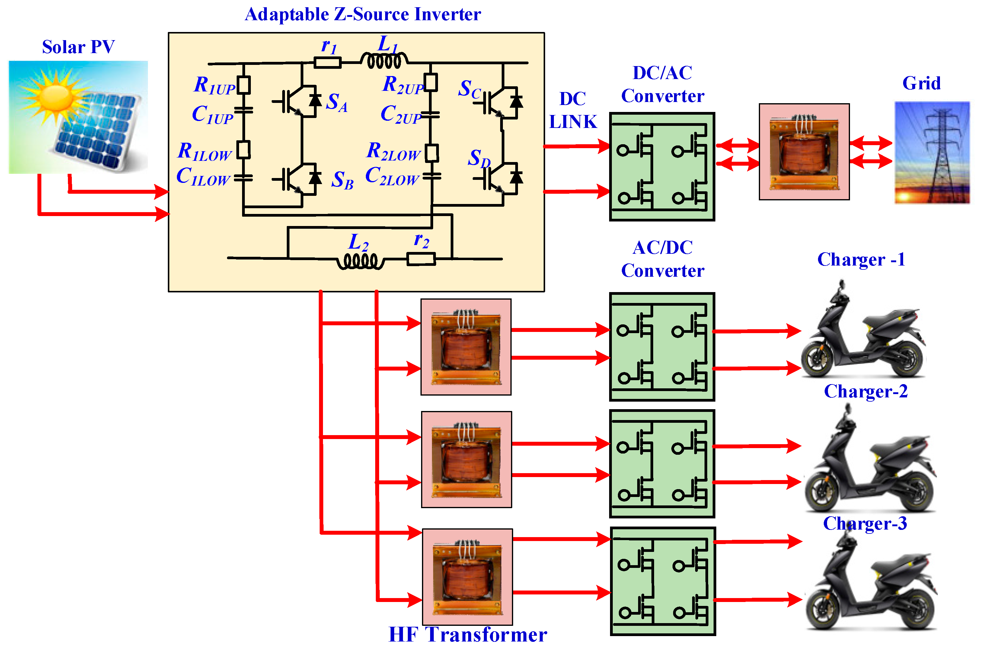
  • An Adaptable Z-Source Inverter was developed for the PV-grid integration-based EV charging station.
  • The capacitor used in the Z-network was split into two equal capacitors to enable the multiport charging option.
  • This modified ZSI was validated in five modes: PV-grid/charger, PV-grid, PV-charger, grid–charger, and charger–grid.
  • The experimental setup was developed with three charging ports for obtaining 250 W at each charger end, which cumulatively produces 750 W output across both chargers with an efficiency of 93.8%.
This paper is organized as follows: the modeling and sizing of the proposed Adaptable Z-Source Inverter components are explained in Section 2, and the different modes of operation of the proposed AZSI are discussed in Section 3. The simulation model is discussed in Section 4. The experimental results are discussed in Section 5. The loss calculation is discussed in Section 6. Section 7 concludes the proposed AZSI.

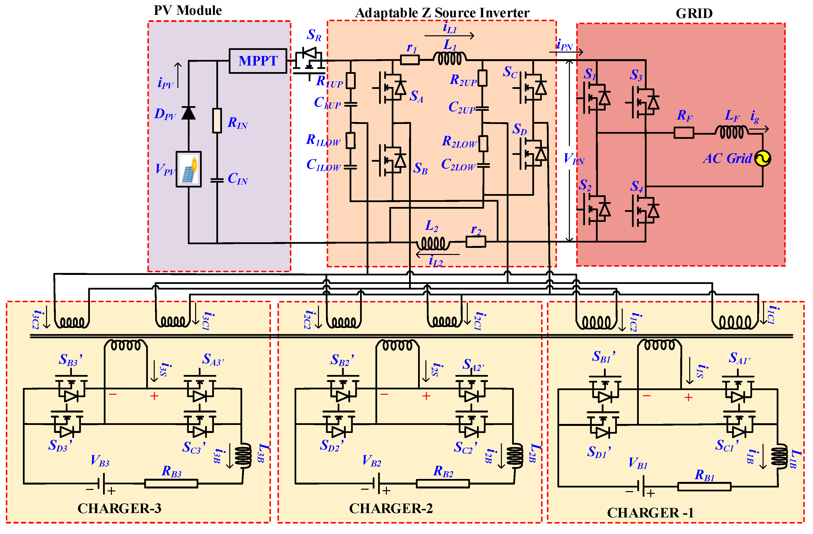
2. Modeling and Sizing of the Proposed Adaptable Z-Source Inverter Components

The ZSI generates boost or buck output, doubling the output due to the presence of dual capacitors and dual inductors next to the DC supply. The ZSI can perform symmetrical operations in both shoot-through and non-shoot-through states. Switches S1 and S4 are turned on in the first cycle to generate a positive output voltage, while switches S2 and S3 are closed in the next cycle to generate a negative output voltage. When all four switches are turned on during a cycle change, this is referred to as the “shoot-through state” (ST). In this situation, the output is continuous. When the output is discontinuous, the mode of operation is in a non-shoot-through state (NST); at this state, all four switches are in the OFF position.
The proposed work involves modifying the conventional Z-source inverter to create a multiport EV charger. In the traditional topology, the inverter has two capacitors, C1 and C2, which are split into two equal-rated capacitors to divide voltage. The AZSI for the multiport charging environment is depicted in Figure 1, and its equivalent circuit diagram is shown in Figure 2. The conventional capacitors C1 and C2 are replaced with four capacitors: C1UP, C1LOW, C2UP, and C2LOW. The charging station is powered by a PV system and a grid. The charging station is operated with a PV source and battery. When the PV generates power more than the charging demands, the surplus power is delivered to the grid.
Similarly, the grid supplies the charging demand when the PV source is not available. The conventional ZSI can handle this scenario, but multiport tapping cannot be achieved. However, the modified inverter topology proposed in this work can provide the multiport option using the high-frequency transformers (HFTs) tapped between the splitter capacitors. The primary side of the HFT is connected to the AZSI and the secondary side is connected to the charging port. A switch SR is used between the PV and AZSI to restrict the reverse current to the PV from the battery and grid. Four H-Bridge Converters (HBCs) are used between the AZSI to grid and battery. The converters are built with MOSFET switches, and these switches are operated with PWM pulses.
A Maximum Power Point Tracking (MPPT) controller is used in between the AZSI and solar PV, as shown in Figure 2. The MPPT controller is useful for tracking maximum power when the PV is operating under uncertain environmental conditions like partial shading. In this work, the conventional Perturb and Observe (P&O) MPPT algorithm is used to achieve the maximum power point [29,30].
The inductor current (iL) and the capacitor voltage (VC) across the switches and current can be written as Equations (1) and (2):
i L = i L 1 = i L 2
V C = V C 1 = V C 2
The shoot-through (ST) state is determined by the switching frequency FSW and the duty cycle DO. The voltage across the capacitors is represented by Equation (3):
V C = 1 D O 1 2 D O V P V
The dc-link voltage VPN is given as Equation (4):
V P N = 1 1 2 D O V P V
The power ratio between the AC and DC sides of the ZSI is given as Equation (5):
( 1 D O ) V P N I P N = v g r m s i g r m s
The AC voltage of the AZSI converter is assumed as Equation (6):
V g = M V P N
where Vg is the AC voltage of the AZSI, grid voltage vg is Vgsin ω t , M is the modulation index, VPN is the dc-link voltage, and IPN is the dc-link current. The ZSI’s RMS output voltage can be expressed as Equation (7) and voltage across the capacitor as (8):
V g r m s = M V P V 2 1 2 D O
V C = 2 V B
where VPV is the PV voltage, VPN is the dc-link voltage, IPN is the dc-link current, M is the modulation index, and VB is the battery voltage. Maximum battery voltage and minimum PV input voltage are used to analyze the duty ratio of ST operation (voltage across the capacitors), as given in Equation (9):
D O m a x = 2 V B m a x V p v m i n 4 V B m a x V p v m i n
D O m a x = 2 × 500 100 4 × 500 100 = 900 1900 = 0.4737
where DOmax is the maximum ST duty ratio.

2.1. Inductor L1 and L2 Design

The inductors L1 and L2 are built with a peak-to-peak high-frequency current ripple considered as 10% or 20%. The values of inductors L1 and L2 can be designed using Equation (10):
L 1 = L 2 = V C m a x D O m a x 2 Δ i L f

2.2. Capacitor C1 and C2 Design

The design of the capacitors reduces second-order harmonics in capacitor voltages. Suppressing the harmonics may cause the system to become complex. Hence, an active power filter is utilized to minimize capacitance. The capacitor values can be expressed as Equation (11):
C 1 U P = C 1 L O W = C 2 U P = C 2 L O W = 2 C 1 = 2 C 2 = 2 P 2 ω Δ V C V C
where VC represents the maximum permissible voltage ripple, and VC denotes the average voltage across capacitors VC1 and VC2. The symbol ω (rad/s) represents second-order harmonics. For the proposed topology, the maximum capacitor voltage rating is at least twice as high as the peak voltage of the energy storage device clamped across it.
The proposed inverter topology can operate in five different modes such as Mode-I (PV to grid and charger), Mode-II (PV to grid), Mode-III (PV to charger), Mode-IV (grid to charger), and Mode-V (charger to grid) as shown in Figure 3a–e.
The capacitor voltage and inductor current from the equivalent circuit model can be expressed as Equations (12)–(15):
C H B V H B = i L i I N 1 4 i B
L B i B = V H B ( i L i l N ) R H B 1 2 R H B + 2 R B i B V B
C = 1 2 C H B
r c = 1 2 R H B
The average transformer current is zero, whereas the average current entering the MOSFETs is 1/4 ILB (50 percent due to the parallel primaries sharing current and another 50 percent due to the duty cycle). Fifty percent of VC is the average recovered secondary voltage. The DC-DC converters are connected to the battery load through the parallel branch from the Z-circuit capacitors.

3. Modes of Operations

The proposed AZSI was validated in five different modes of operations as follows: (1) Mode-I (PV to grid and charger), (2) Mode-II (PV to grid), (3) Mode-III (PV to charger), (4) Mode-IV (grid to charger), and (5) Mode-V (charger to grid).

3.1. Different Modes

3.1.1. Mode-I (PV to Grid and Charger)

In this mode of operation, the charging stations are completely dependent on the PV system. When the PV system can generate the required load at the charging side, excess power is delivered to the grid. The PV system generates the rated power, which is sufficient for the charging station. So, the AZSI allows the PV power to charge the batteries in the charging stations, and surplus power is sent to the grid, which reduces the dependency on fossil fuels. The AZSI can manage this power flow from the PV to the grid and the PV to the battery. The switches in all HBCs are operated with 50% of the duty cycle, and the switches in the AZSI are operated with 25% of the duty cycle. This allows for delivery of the power to the grid and the battery. The current flow of this mode is shown in Figure 3a.

3.1.2. Mode-II (PV to Grid)

In this mode, the charging stations are inactive, and the PV power generation is completely delivered to the grid. The batteries at the charging stations are considered as if they are fully charged or the load demand at the charging station is zero. In this case, the charging stations do not require power from the PV or grid. So, all the power generated from the PV system will be delivered to the grid. The AZSI delivers power only to the grid and blocks the power flow toward the charging stations. The switches of the HBCon the grid side are operated with 50% of the duty cycle, and the switches in the AZSI are operated with 25% of the duty cycle, where the switches of the HBC at the charger side are zero. By operating the AZSI with these controls, the power flow can be controlled. The current flow of this mode is shown in Figure 3b.

3.1.3. Mode-III (PV to Charger)

In this mode of operation, the charging demand is very high, whereas the PV generation is below the required level of demand. In this case, the PV is not capable of meeting the entire load demand on the charger side. However, the demand needs to be met. For that, the grid will supply the remaining power to the charger to meet the demand. In this mode, both grid and PV systems supply power to the charger. The AZSI delivers power only to the charger and blocks the power flow toward the grid. The switches of the HBC on the charger side are operated with 50% of the duty cycle, and the switches in the AZSI are operated with 25% of the duty cycle, where the switches of the HBC on the grid side are zero. By operating the AZSI with these controls, the power flow can be controlled. The current flow of this mode is shown in Figure 3c.

3.1.4. Mode-IV (Grid to Charger)

In this mode, the PV system does not generate any power due to the unavailability of sunlight or because of some faults. However, the charging station is operated under high demand, which needs to be supplied. So, the grid takes on the charge to supply the charging station. The grid will supply all the required demand at the charging station. The AZSI regulates power between the grid and charger, and the power flow toward the PV is blocked by the bypass diode.
The switches of the HBC on the grid side and charger are operated with 50% of the duty cycle, and the switches in the AZSI are operated with 25% of the duty cycle. By operating the AZSI with these duty cycles, the power flow can be controlled. The current flow of this mode is shown in Figure 3d.

3.1.5. Mode-V (Charger to Grid)
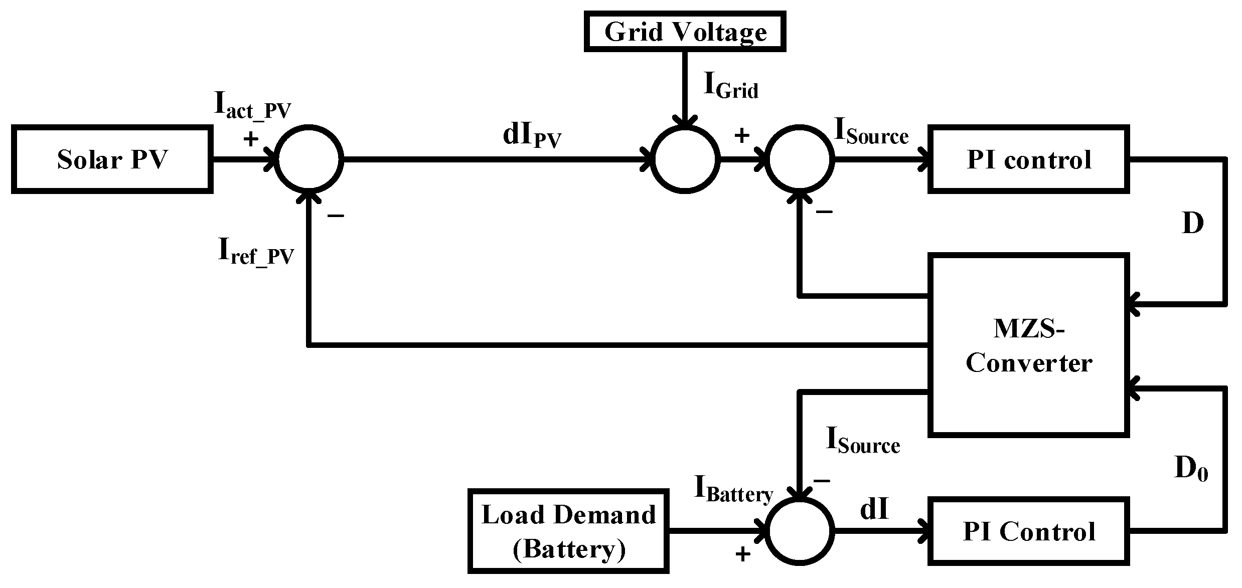
In this mode, it is considered that the PV is completely inactive, and the charging station is inactive. The grid operates on a high level of demand. The AZSI regulates the power stored in the battery to the grid to support it in supplying the maximum demand. This mode reduces the stress on the grid and improves its stability. The AZSI regulates power between the charger and the grid, and the power flow toward the PV is blocked by the bypass diode. The switches of the HBC on the grid side and charger are operated with 50% of the duty cycle, and the switches in the AZSI are operated with 25% of the duty cycle. By operating the AZSI with these duty cycles, the power flow can be controlled. The current flow of this mode is shown in Figure 3e.

3.2. Controller

The overall system designed in this work is made up of three interconnected control loops: PV-battery, grid-to-battery, and battery-to-grid. Each loop has a distinct function in regulating the power flow between the PV system, battery, and grid.

3.2.1. PV-Battery Loop

This loop enables the charging of the battery using the power provided by the PV system. This loop ensures that the battery receives the maximum power from the PV source while remaining below safe operating conditions for voltage and current. The PI controller in this loop continuously monitors the PV output and battery state of charge (SOC) to calculate the optimal charging rate. It regulates the charge current by adjusting the power converter’s duty cycle connected to the PV system and the battery. The PI controller’s proportional term controls instant variations in the PV power output, while the integral term controls steady-state errors in battery charging. The functional block diagram of the PI controller used in this work is shown in Figure 4.

3.2.2. Grid-to-Battery Loop

The grid-to-battery loop allows the system to use grid electricity to charge the battery and its internal charge. This loop monitors the grid voltage, battery SOC, and charging requirements to determine when to use the grid. The PI controller in this loop controls the duty cycle of the power converter linking the grid and the battery to control the charging current. The controller compares the battery’s SOC to the intended set point and adjusts the charging rate. The proportional term is adapted to changes in grid power availability in real time, while the integral term assures that the battery SOC is aligned with the intended set point.

3.2.3. Battery-to-Grid Loop

The battery-to-grid loop allows the system to supply electrical power from the battery back to the grid during periods of high demand or peak prices. This loop analyzes grid conditions, battery SOC, and grid power requirements to determine when electricity should be discharged from the battery to the grid. The PI controller in this loop adjusts the duty cycle of the power converter linking the battery and the grid to control the power flow. The controller compares grid demand to the battery’s available capacity and adjusts the discharge rate accordingly. The proportional term responds to immediate changes in grid demand, but the whole term ensures that the battery capacity is comparable to the grid requirements. This control system can effectively regulate the power flow between the PV, battery, and grid by utilizing the three interconnected control loops. To maintain optimum functioning, the PI controllers in each loop constantly monitor the relevant variables, compare them to desired points, and change the duty cycles of the power converters. This method ensures that the battery is powered efficiently using both the PV and grid sources, while also allowing the battery to provide power back to the grid as needed.

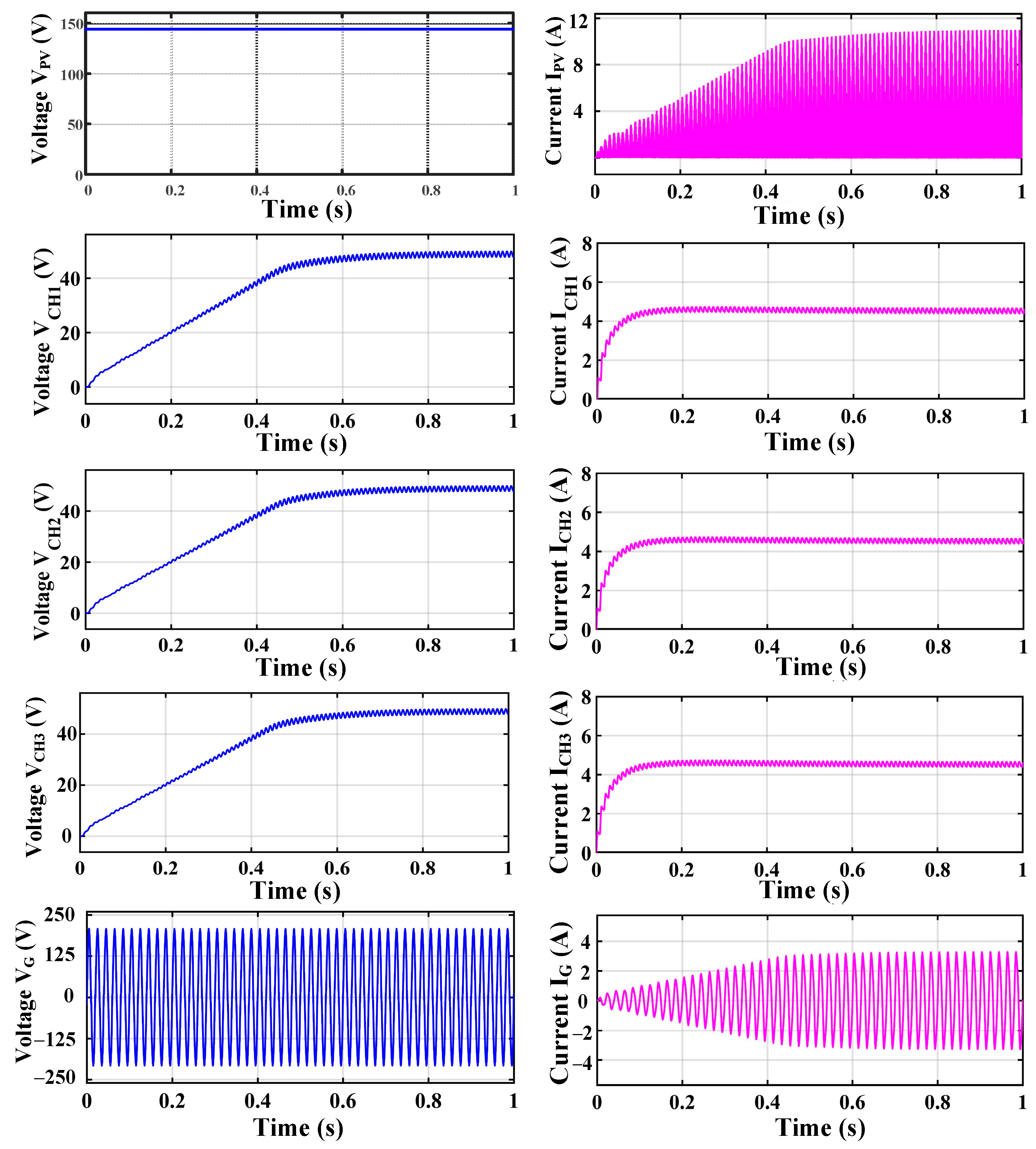
4. Simulation Analysis Results

The proposed topology was developed using MATLAB/Simulink® 2016a software. A DC source was used as the PV source, with a maximum output voltage of 144 V DC. This source was connected to the AZSI circuit, constructed using MOSFET switches. The PWM technique was used to generate switching pulses with a frequency of 25 kHz. A H-bridge converter was linked between the AZSI and the grid, and the conventional ZSI capacitors were split into two equal capacitors to create a multiport charger. A high-frequency transformer with a winding ratio of 2:1 was connected across these two capacitors. The charger was linked to these three HFTs via the battery arrangement. This simulation was modeled with the necessary calculations for capacitors, inductors, and switching frequency using Equations (1)–(15).
The adaptable Z-source converter designed for EV charge applications was carefully constructed to cater to various operational modes, ensuring flexibility in power supply and increased reliability for the charging station. The charging station utilizes both photovoltaic (PV) panels and the grid. The PV array’s specifications are as follows: it can generate up to 1500 W of power, operating at a 144 V voltage and delivering a current of 10.32 A. A conventional Perturb and Observe (P&O) MPPT algorithm is used to achieve the maximum power point.
There are five distinct operational modes for this converter:
  • PV to grid and charger: In this mode, the PV system supplies power to the battery, and the excess power is delivered to the grid. The PV system generates a rated power of 1500 W power with a voltage of 144 V and a current of 10.32 A. The PV delivers 750 W power to the three chargers and 750 W power to the grid.
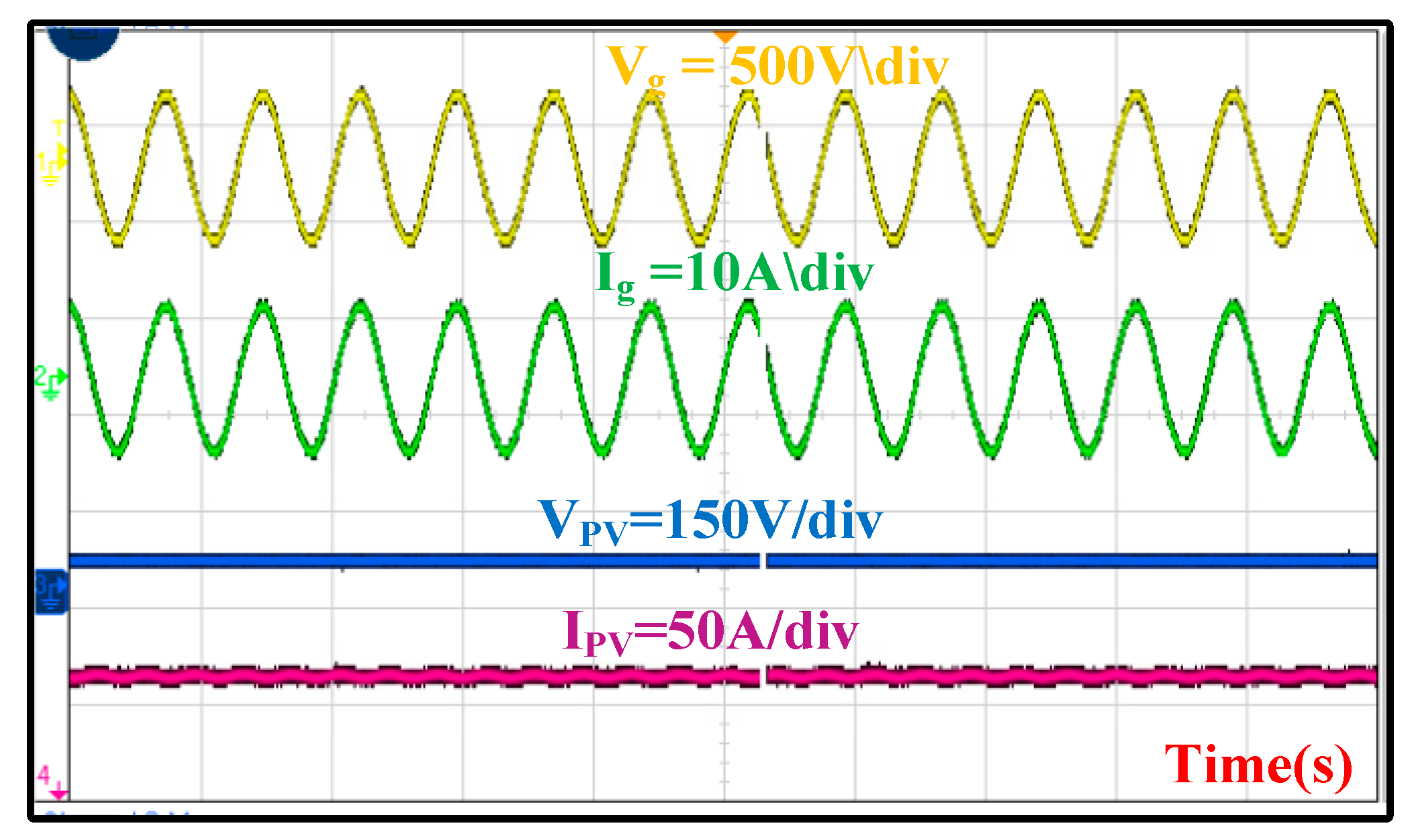
  • PV to grid: In this mode, the charging stations are inactive, and the PV power generation is completely delivered to the grid. To provide power to the grid, the PV continues to operate at the rated power of 144 V and 10.42 A. The grid receives 230 V, and 63 A is provided to the grid.
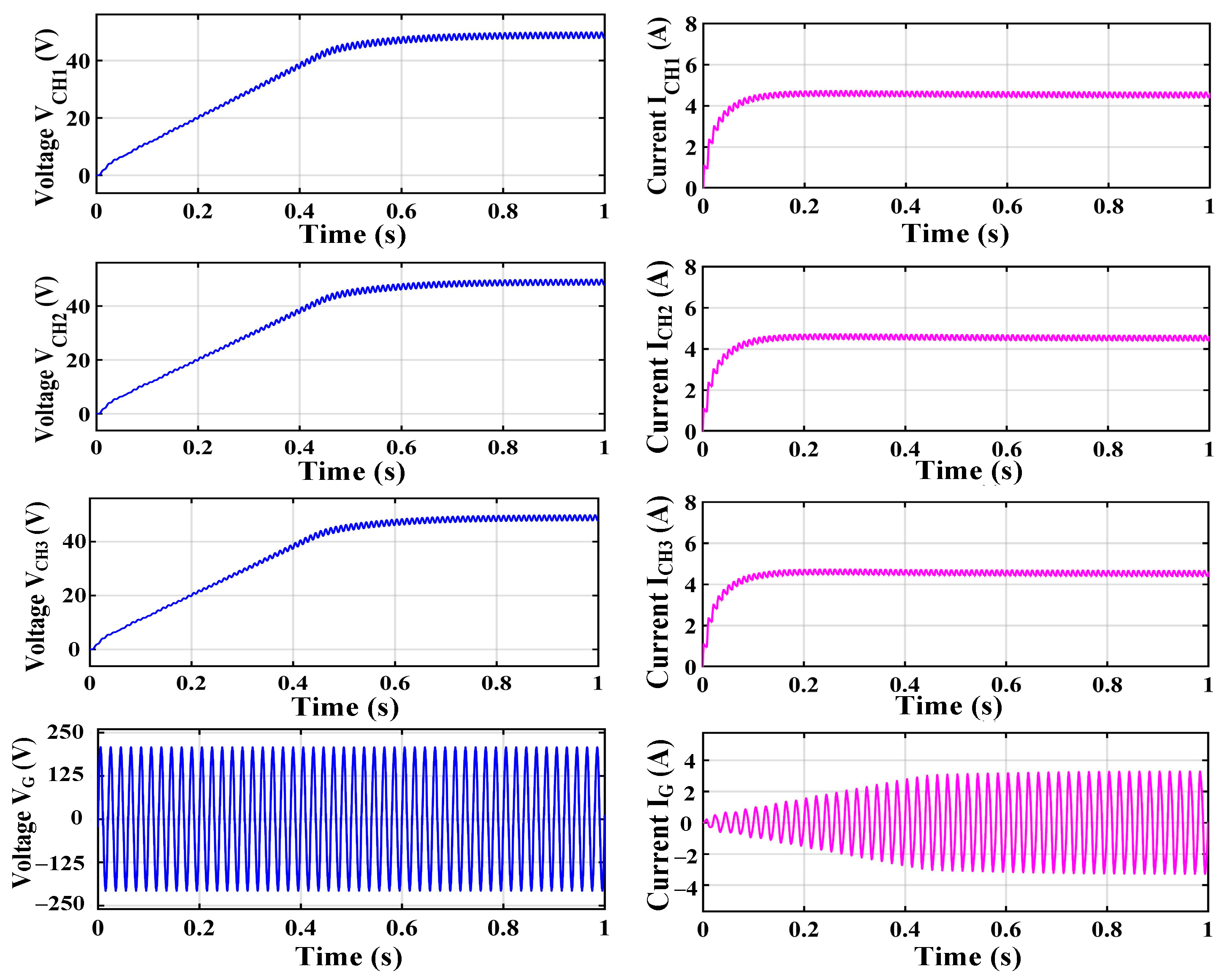
  • PV to charger: In this mode of operation, the PV generates half of the rated power, and the grid is operated on low demand. The PV-generated power is delivered only to the chargers. The three chargers are powered by Charger 1 at 47.9 V and 4.93 A, Charger 2 at 47.8 V and 4.86 A, and Charger 3 at 48.2 V and 4.87 A.
  • Grid to charger: This mode supplies the power from the grid to the charging stations. The PV does not generate power, and the charging station is in demand. So, the grid delivers the power requirement to the charging station.
  • Charger to grid: In this mode, it is considered that the PV is completely inactive, and the charging station is inactive. The grid operates at a high level of demand. The AZSI regulates the power stored in the battery to the grid to support it in supplying the maximum demand.
In Mode-I, the PV supplies power to the grid and the battery when all seventeen switches used in the converter are turned ON. The HBC switches are operated with a 50% duty ratio, and the AZSI is performed with a 25% duty ratio. The obtained waveforms for this case showed that the PV supplies nearly 750 W of power to the two charging stations and 750 W of power to the grid. The total power delivered to the grid and charging stations was around 1407 W, with an efficiency of 93.8%. Similar analyses were carried out for the other modes, and the corresponding waveforms are shown in Figure 5, Figure 6, Figure 7, Figure 8 and Figure 9. Table 1 gives the specifications and calculated parameters.
The results show that the proposed AZSI had 93.6% efficiency in all cases and an enhanced performance and multiport charging option. However, the real-time performance of the proposed AZSI needs to be validated to reduce the consequences of challenging factors in practical applications.

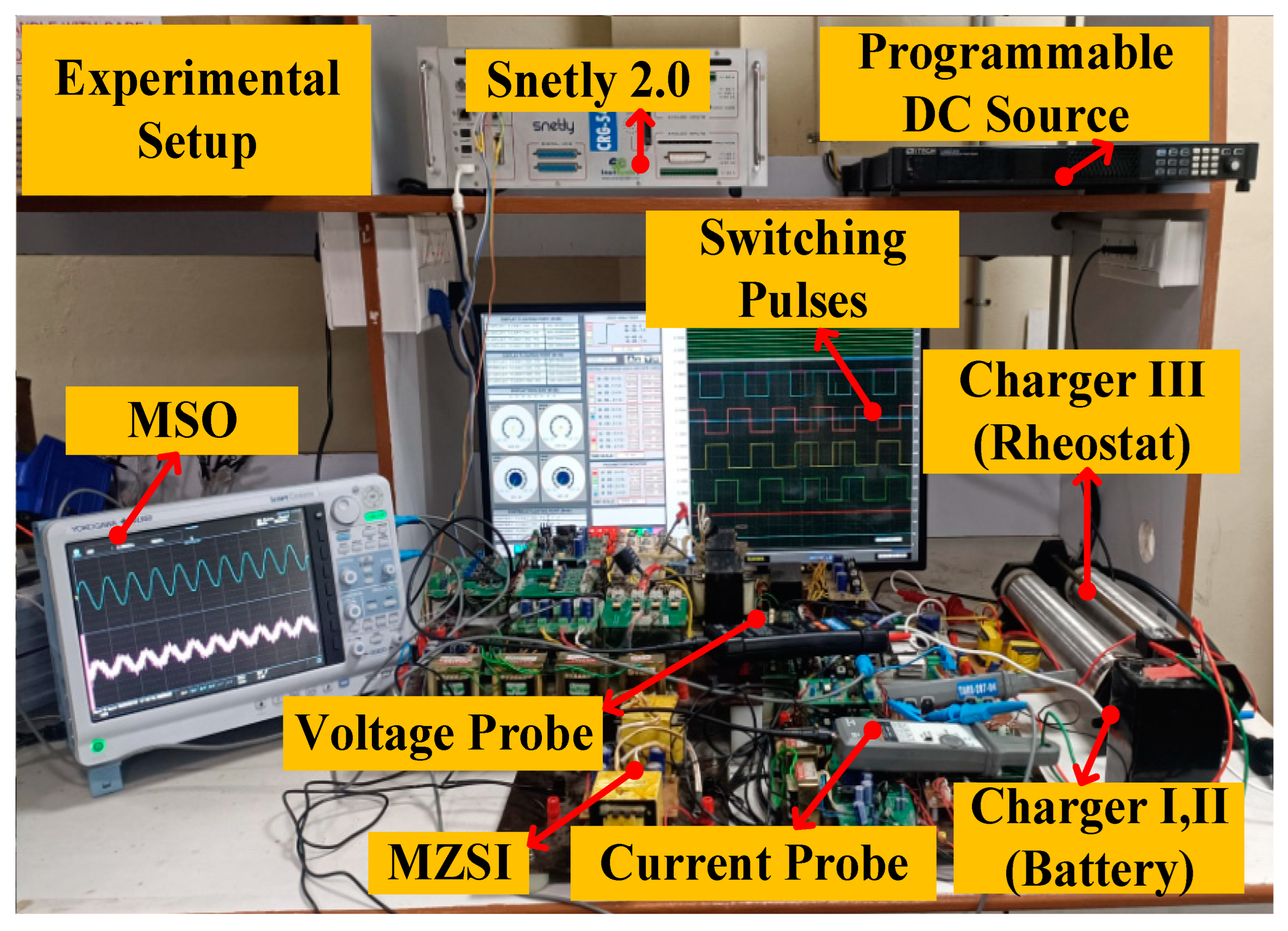
5. Experimental Results

The experimental setup of the proposed modified PV-tied AZSI multiport EV charger was built and used to validate all the modes with the help of the Snetly 2.0 FPGA controller, as shown in Figure 10. A 4 kW programmable bidirectional DC supply was used as a PV source (PV Emulator) and 48 V, 10 Ah Li-ion, and a rheostat were used as the loads. The values of each parameter used in the experimental setup are listed in Table 2. The solar PV simulator (4 kW, ITECH, M3904C) is associated with the inbuild P&O MPPT algorithm.
The HBC1 output terminal is connected to the grid through an AC for the grid supply, and a mixed signal oscilloscope (YOKOGAWA DL950) is used to observe the output. Four HBCs, three HFTs, and one AZSI were connected between the programmable DC source, battery, rheostat, and grid. Along with this inverter, four HBCs were designed using MOSFETs. The operating modes, the AZSI and HBC duty cycle switches, are operated at 25% and 50%, respectively. Figure 11 shows the experimental results of the PV to grid and battery (Mode-I). The PV emulator is set to produce the power (VPV = 144 V, IPV = 10.42 A). The AZSI delivers the required dc-link VPN and IPN to the grid. At the same instant, it supplies 48.1 V, 4.65 A power to Charger 1 and 47.8 V, 4.79 A power to Charger 2 and 47.7 V, 4.74 A power to Charger 3 via the HBCs. The corresponding waveforms are shown in Figure 11. It shows the converter’s performance used for the PV-grid integrated EV charging station efficiently delivering power to the grid and battery with minimum losses and lower THD values. The losses associated with the Mode-I operation are calculated in the following section. Similarly, other modes: PV to grid, PV-charger, grid–charger, and charger to grid are validated as follows:
PV to Grid: In this operation mode, the charging station is not functioning. During this time, all the power generated by the PV is delivered to the grid, which reduces the dependency on conventional energy sources. In this mode, the PV operates on the rated power of 1500 W with 144 V, 10.42 A. All the power is delivered to the grid through the MZSI, which regulates the voltage to 230 V to match the grid voltage. The grid receives the 230 V, 6.3 A AC power. This reduces the need for power from conventional sources because of the generating station of the grid supply, and the corresponding waveforms are shown in Figure 12.
PV to charger: In this mode, the PV system is generating power but not at its maximum capacity (e.g., half of its full potential). At the same time, the local grid is not heavily used by its consumers. The power from the solar panels is not going into the regular grid or being used for general appliances. Instead, it is sent directly to three specific chargers:
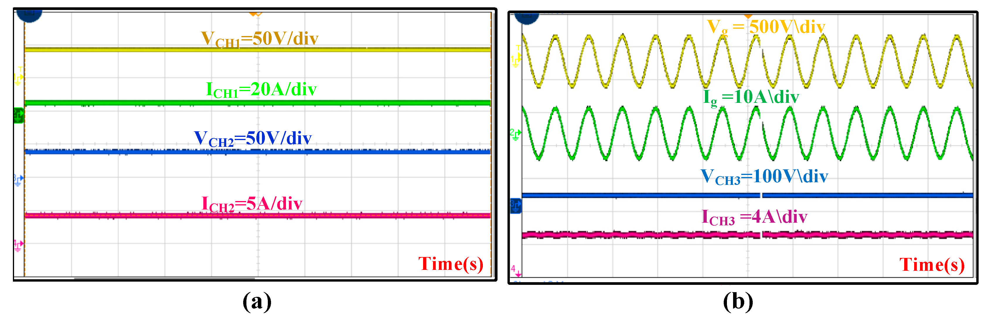
  • Charger 1 receives power at a voltage of 47.9 V and draws a current of 4.93 A.
  • Charger 2 receives power at a voltage of 47.8 V and draws a current of 4.86 A.
  • Charger 3 receives power at a voltage of 48.2 V and draws a current of 4.87 A.
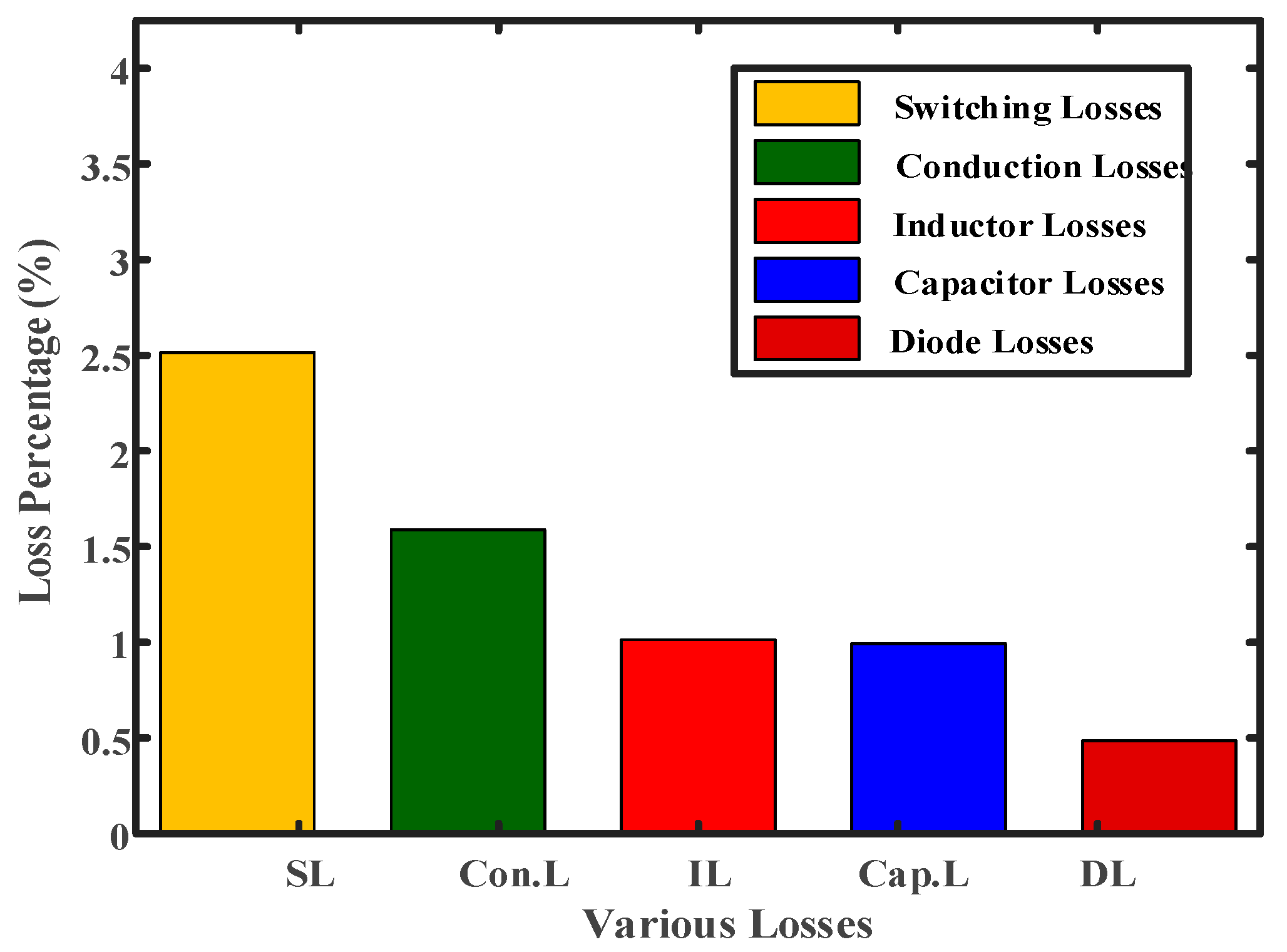
The corresponding waveforms are shown in Figure 13.
Grid to charger: In this mode, the PV system is not generating power due to low irradiation. At the same time, the demand at the charging station is higher than in the normal scenario. The grid supplies the required power to the charging station for supporting the demand, as shown in Figure 14.
Charger to grid: In this mode, it is considered that the PV is completely inactive. The charging station is in an idle position, where there are no vehicles charging. In this scenario, the PV, grid, and charging station’s power regulation is null. During this scenario, the charging station may supply the power to the grid when it operates at its peak demand. This mode of operation reduces the stress on the grid by regulating the power stored in the charging station. The corresponding waveforms of this mode are shown in Figure 15.

6. Loss Calculation

6.1. Loss Calculation

The system’s efficiency depends on the losses involved in the components and semiconductors used in the system. The losses in the AZSI are calculated using rms current and resistance of elements. The rms and average current in the inductors are expressed as Equations (16) and (17). The conduction losses of the inductor (L) are expressed as Equation (18).
I L . R M S = 1 T 0 T i L 2 t d t
I L . a v g = 1 T 0 T i L t d t
P L = I 2 L . R M S R L = I 2 0 1 d 4 2 R L
The rms current, average current, and conduction losses of the capacitor (C) are given in Equations (19)–(21):
I C . R M S = 1 T 0 T i C 2 t d t
I C . a v g = 1 T 0 T i C t d t
P C   = I 2 C . R M S R C   = I 2 0 1 d 2 ( 2 d 1 d 2 d 3 d 4 ) R c
The rms and average current across the switches are given in Equations (22) and (23):
I S . r m s = 1 T 0 T i S 2 t d t
I S . a v g = 1 T 0 T i S t d t
The losses in switches SA, SB, SC, and SD are given as where R1UP, R2LOW, R2UP, and R2LOW are the resistances SA, SB, SC, and SD when they are in the on state, which can be expressed as Equations (24)–(27):
P S A , R M S = I 2 S A , R M S R S   = ( ( I 2 0 d 1 ) / ( 1 d 4 ) 2 ) R S A
P S B , R M S   = I 2 ( S B , R M S ) R S = I 2 0 d 2 1 d 4 2 R S B
P S C , R M S   = I 2 S C , R M S R S = I 2 0 d 3 1 d 4 2 R S C
P S D , R M S   = I 2 S D , R M S R S = I 2 0 d 4 1 d 4 2 R S D
The addition of the losses of switches SA, SB, SC, and SD are expressed as Equation (28):
P S , c o n d = P S A + P S B + P S C + P S D = d 1 I 2 0 1 d 4 2 ( d 1 + d 2 + d 3 + d 4 )   R S
The switching losses of the switches can also be expressed in basic terms as Equation (29):
P S , S W , T o t a l = 1 2 V S I S ( t o n + t o f f ) f s      
The overall switching losses of switches SA, SB, SC, and SD are given as Equation (30):
P S , s w , O v e r a l l = P S A , S W + P S B , S W + P S C , S W + P S D , S W
Similarly, the diode losses of Da1, Da2, Da3, and Da4 can be estimated with Equation (31):
P d c O v e r a l l = [ I D a 1 r m s 2   + I D a 2 r m s 2 + I D a 3 r m s 2 + I D a 4 r m s 2 ] r d    
The rms and average current of the diode are given in (32)–(33):
I r m s   d i o d e = 1 T 0 T i d i o d e 2 t d t
I a v g   d i o d e = 1 T 0 T i d i o d e t d t
It is derived and simplified as Equations (34) and (35):
P d c = [ d m 2 I 0 2 1 d m 2 + 2 l 0 2 1 d m ] r d = [ 2 l 0 2 1 d m [ d m 1 d m + 1 ] ] r d
P d c = 2 l 0 2 1 d m 2 r d
where rd is the resistance of the diode.
The power losses in the AZSI can be measured by combining all the losses associated with the individual components. Therefore, with the help of overall losses Poverall and the output power Pout, the total efficiency of the AZSI can be estimated using Equation (36):
E f f i c i e n c y ,   η = P o u t P o u t     +     P o v e r a l l   l o s s e s × 100

6.2. Stress Analysis

The stress across the switches is calculated based on the voltage and current stress. The voltage stress across the switch and diode is shown in Equations (37) and (38):
V s   s t r e s s = D + d d ( 1 D ) V i n
V D   s t r e s s = V i n ( 1 D )
The current stress across the inductor and diode is shown in Equations (39) and (40):
I L   s t r e s s = D + d d V o R
I D   s t r e s s = n ( D + d ) d V o R
The losses like switching loss, conduction loss, inductor loss, capacitor loss, and diode loss were measured, as shown in Figure 16. The proposed AZSI has an enhanced efficiency of 93.6%. The efficiency of the AZSI was verified using experimentation, and the results show that it is suitable for practical applications. Also, the proposed inverter topology has the potential to provide an effective solution for various applications, including electric vehicle charging infrastructure, renewable energy systems, etc.

7. Conclusions

In this work, an Adaptable Z-Source Inverter (AZSI) is designed and developed for the multiport charging of electric vehicles (EVs). The AZSI is connected between the PV system, grid, and battery. The capacitor used in the normal ZSI is split into two capacitors to enable multiport operation. This proposed inverter is modeled in MATLAB/Simulink® and constructed in an experimental setup. The charging station has three charging ports of 750 W load and is powered with 1500 W solar PV and the grid. The performance of the AZSI is validated under different modes of operation. In the first case, the PV supplies 1500 W to the AZSI, which delivers 678 W to the three battery charging ports and 739 W to the grid with an efficiency of 93.8%. Compared with the conventional ZSI, the proposed AZSI has enhanced efficiency and provides multiport charging options. The proposed AZSI has many advantages over the ZSI in terms of better efficiency, a simple control method, simple construction, and low cost. The inferences from the proposed AZSI pave the way for additional study into optimizing the AZSI architecture, examining scalability alternatives, measuring its performance in real-world scenarios, and incorporating advanced control and communication systems for seamless operation and grid integration.

Author Contributions

Conceptualization, R.G. and B.C.; data curation, R.G. and B.C.; formal analysis, R.G. and B.C.; investigation, R.G. and B.C.; methodology, R.G. and B.C.; software, R.G and B.C.; writing—original draft, R.G. and B.C.; writing—review and editing, R.G. and B.C. All authors have read and agreed to the published version of the manuscript.

Funding

This research was funded by the Department of Science and Technology, Government of India, Promotion of University Research and Scientific Excellence (PURSE), SR/PURSE/2021/65.

Data Availability Statement

Data are contained within the article.

Acknowledgments

This work was partly supported by the Department of Science and Technology, Government of India, Promotion of University Research and Scientific Excellence (PURSE).

Conflicts of Interest

The authors declare no conflicts of interest.

References

  1. Nezamuddin, O.N.; Nicholas, C.L.; dos Santos, E.C. The Problem of Electric Vehicle Charging: State-of-the-Art and an Innovative Solution. IEEE Trans. Intell. Transp. Syst. 2022, 23, 4663–4673. [Google Scholar] [CrossRef]
  2. Khan, S.A.; Md Islam, R.; Guo, Y.; Zhu, J. A New Isolated Multiport Converter with Multi-Directional Power Flow Capabilities for Smart Electric Vehicle Charging Stations. IEEE Trans. Appl. Supercond. 2019, 29, 0602504. [Google Scholar] [CrossRef]
  3. Verma, A.; Singh, B.; Chandra, A.; Al-Haddad, K. An Implementation of Solar PV Array Based Multifunctional EV Charger. In Proceedings of the 2018 IEEE Transportation Electrification Conference and Expo (ITEC), Long Beach, CA, USA, 13–15 June 2018. [Google Scholar] [CrossRef]
  4. Zhu, H.; Zhang, D.; Zhang, B.; Zhou, Z. A Nonisolated Three-Port DC–DC Converter and Three-Domain Control Method for PV-Battery Power Systems. IEEE Trans. Ind. Electron. 2015, 62, 4937–4947. [Google Scholar] [CrossRef]
  5. Wu, S.-T.; Yang, B.-Y. Design and Implementation of an Isolated Bidirectional Phase-Shift Full-Bridge Converter with High Transformation Ratio. IEEE Access 2023, 11, 17945–17955. [Google Scholar] [CrossRef]
  6. Li, T.; Cheng, Q. A comparative study of Z-source inverter and enhanced topologies. CES Trans. Electr. Mach. Syst. 2018, 2, 284–288. [Google Scholar] [CrossRef]
  7. Rajakaruna, S.; Jayawickrama, L. Steady-State Analysis and Designing Impedance Network of Z-Source Inverters. IEEE Trans. Ind. Electron. 2010, 57, 2483–2491. [Google Scholar] [CrossRef]
  8. Dong, S.; Zhang, Q.; Cheng, S. Analysis of Critical Inductance and Capacitor Voltage Ripple for a Bidirectional Z -Source Inverter. IEEE Trans. Power Electron. 2015, 30, 4009–4015. [Google Scholar] [CrossRef]
  9. Nasr Esfahani, F.; Darwish, A.; Williams, B.W. Power Converter Topologies for Grid-Tied Solar Photovoltaic (PV) Powered Electric Vehicles (EVs)—A Comprehensive Review. Energies 2022, 15, 4648. [Google Scholar] [CrossRef]
  10. Varesi, K.; Hossein Hosseini, S.; Sabahi, M.; Babaei, E.; Saeidabadi, S.; Vosoughi, N. Design and Analysis of a Developed Multiport High Step-Up DC–DC Converter with Reduced Device Count and Normalized Peak Inverse Voltage on the Switches/Diodes. IEEE Trans. Power Electron. 2019, 34, 5464–5475. [Google Scholar] [CrossRef]
  11. Shreya, K.; Srivastava, H.; Kumar, P.; Ramanathan, G.; Madhavan, P.; Bharatiraja, C. CUK converter fed resonant LLC converter based electric bike fast charger for efficient CC/CV charging solution. J. Appl. Sci. Eng. 2021, 24, 331–338. [Google Scholar] [CrossRef]
  12. Bharatiraja, C.; Lakshmikhandan, K.; Kamalesh, M.S.; Rajasekaran, D.; Twala, B. A Non-Isolated High-Gain DC to DC Converter Connected Multi-Level Inverter for Photovoltaic Energy Sources. J. Appl. Sci. Eng. 2021, 24, 415–422. [Google Scholar] [CrossRef]
  13. Rathore, V.; Reddy, S.R.P.; Rajashekara, K. An Isolated Multilevel DC–DC Converter Topology with Hybrid Resonant Switching for EV Fast Charging Application. IEEE Trans. Ind. Appl. 2022, 58, 5546–5557. [Google Scholar] [CrossRef]
  14. Jang, Y.; Sun, Z.; Ji, S.; Lee, C.; Jeong, D.; Choung, S.; Bae, S. Grid-Connected Inverter for a PV-Powered Electric Vehicle Charging Station to Enhance the Stability of a Microgrid. Sustainability 2021, 13, 14022. [Google Scholar] [CrossRef]
  15. Elmorshedy, M.F.; Essawy, I.J.A.; Rashad, E.M.; Islam, M.R.; Dabour, S.M. A Grid-Connected PV System Based on Quasi-Z-Source Inverter With Maximum Power Extraction. IEEE Trans. Ind. Appl. 2023, 59, 6445–6456. [Google Scholar] [CrossRef]
  16. Siwakoti, Y.P.; Peng, F.Z.; Blaabjerg, F.; Loh, P.C.; Town, G.E. Impedance-Source Networks for Electric Power Conversion Part I: A Topological Review. IEEE Trans. Power Electron. 2015, 30, 699–716. [Google Scholar] [CrossRef]
  17. Kumar, K.V.; Reddivari, R.; Jena, D. A Comparative Study of Different Capacitor Voltage Control Design Strategies for Z-Source Inverter. IETE J. Res. 2019, 68, 1443–1453. [Google Scholar] [CrossRef]
  18. Abbasi Bolaghi, J.; Taheri, A.; Babaei, M.H.; Gholami, M.; Harajchi, S. A Quasi-Z-Source Inverter with a Network Capacitor-Inductor. IETE J. Res. 2023, 1–16. [Google Scholar] [CrossRef]
  19. Sampath, S.; Rahiman, Z.; Chenniappan, S.; Sundaram, E.; Subramaniam, U.; Padmanaban, S. Efficient Multi-Phase Converter for E-Mobility. World Electr. Veh. J. 2022, 13, 67. [Google Scholar] [CrossRef]
  20. Fakhrooeian, P.; Pitz, V. A New Control Strategy for Energy Management of Bidirectional Chargers for Electric Vehicles to Minimize Peak Load in Low-Voltage Grids with PV Generation. World Electr. Veh. J. 2022, 13, 218. [Google Scholar] [CrossRef]
  21. Sun, Q.; Xie, H.; Liu, X.; Niu, F.; Gan, C. Multiport PV-Assisted Electric-Drive-Reconstructed Bidirectional Charger With G2V and V2G/V2L Functions for SRM Drive-Based EV Application. IEEE J. Emerg. Sel. Top. Power Electron. 2023, 11, 3398–3408. [Google Scholar] [CrossRef]
  22. Assadi, S.A.; Gong, Z.; Coelho, N.; Zaman, M.S.; Trescases, O. Modular Multiport Electric-Vehicle DC Fast-Charge Station Assisted by a Dynamically Reconfigurable Stationary Battery. IEEE Trans. Power Electron. 2023, 38, 6212–6223. [Google Scholar] [CrossRef]
  23. Tran, V.T.; Islam, M.R.; Muttaqi, K.M.; Farrok, O.; Kiran, M.R.; Sutanto, D. A Novel Universal Magnetic Power Plug to Facilitate V2V/V2G/G2V/V2H Connectivity for Future Grid Infrastructure. IEEE Trans. Ind. Appl. 2022, 58, 951–961. [Google Scholar] [CrossRef]
  24. Tashakor, N.; Farjah, E.; Ghanbari, T. A Bidirectional Battery Charger with Modular Integrated Charge Equalization Circuit. IEEE Trans. Power Electron. 2017, 32, 2133–2145. [Google Scholar] [CrossRef]
  25. Ravindran, M.A.; Nallathambi, K.; Vishnuram, P.; Rathore, R.S.; Bajaj, M.; Rida, I.; Alkhayyat, A. A Novel Technological Review on Fast Charging Infrastructure for Electrical Vehicles: Challenges, Solutions, and Future Research Directions. Alex. Eng. J. 2023, 82, 260–290. [Google Scholar] [CrossRef]
  26. Sandoval, M.; Cardenas, V.; Barrios, M.A.; Garcia, M.G.; Alcala, J. Multiport Isolated link with Current-Fed Z-Source Converters to Manage Power Imbalance in PV Applications. Electronics 2020, 9, 280. [Google Scholar] [CrossRef]
  27. Say, G.; Hosseini, S.H.; Esmaili, P. Hybrid Source Multi-Port Quasi-Z-Source Converter with Fuzzy Logic-Based Energy Management. Energies 2023, 16, 4801. [Google Scholar] [CrossRef]
  28. Rostami, S.; Abbasi, V.; Parastesh, M. Design and Implementation of a Multiport Converter Using Z-Source Converter. IEEE Trans. Ind. Electron. 2021, 68, 9731–9741. [Google Scholar] [CrossRef]
  29. Madasamy, P.; Kumar, V.S.; Sanjeevikumar, P.; Holm-Nielsen, J.B.; Hosain, E.; Bharatiraja, C. A three-phase transformerless T-Type- NPC-MLI for grid connected PV systems with common-mode leakage current mitigation. Energies 2019, 12, 2434. [Google Scholar] [CrossRef]
  30. Prakash, G.; Subramani, C.; Bharatiraja, C.; Shabin, M. A low cost single phase grid connected reduced switch PV inverter based on Time Frame Switching Scheme. Inter. J. Electr. Power Energy Syst. 2016, 77, 100–111. [Google Scholar] [CrossRef]
Figure 1. Functional block diagram of the proposed method.
Wevj 15 00031 g001
Figure 2. Circuit diagram of the proposed AZSI.
Wevj 15 00031 g002
Figure 3. Various modes of operation: (a) Mode-I (PV to grid and charger), (b) Mode-II (PV to grid), (c) Mode-III (PV to charger), (d) Mode-IV (grid to charger), and (e) Mode-V (charger to grid).
Wevj 15 00031 g003
Figure 4. Functional block diagram of the PI controller.
Wevj 15 00031 g004
Figure 5. Simulation waveforms of Mode-I (PV to grid and charger).
Wevj 15 00031 g005
Figure 6. Simulation waveforms of Mode-II (PV to grid).
Wevj 15 00031 g006
Figure 7. Simulation waveforms of Mode-III (PV to charger).
Wevj 15 00031 g007
Figure 8. Simulation waveforms of Mode-IV (grid to charger).
Wevj 15 00031 g008
Figure 9. Simulation waveforms of Mode-V (charger to grid).
Wevj 15 00031 g009
Figure 10. Photograph of the experimental arrangement of AZSI.
Wevj 15 00031 g010
Figure 11. (a) Capacitor voltage, (b) inductor voltage and inductor current, (c) grid voltage and current, and (d) charger output voltage and current.
Wevj 15 00031 g011
Figure 12. PV and grid voltage and current.
Wevj 15 00031 g012
Figure 13. (a) PV voltage and current. (b) Charger output voltage and current.
Wevj 15 00031 g013
Figure 14. (a) Grid voltage and current. (b) Charger output voltage and current.
Wevj 15 00031 g014
Figure 15. (a) Charger output voltage and current. (b) Grid voltage and current.
Wevj 15 00031 g015
Figure 16. Various losses in the AZSI.
Wevj 15 00031 g016
Table 1. Simulation Parameters.
S.NoParametersValue
1.Inductor value, L1950 μH
2.Inductor value, L2950 μH
3.Input capacitor, Cin220 µF
4.Filter Inductance, Lf7.6 mH
5.Switching frequency (AZSI), FSW25 kHz
6.Switching frequency (HBC), fs50 kHz
Table 2. Hardware parameters.
S.NoParametersValue
1.PV voltage, VPV144 V
2.Grid voltage Vg230 V
3.Output voltage, VCH148 V
4.Output voltage, VCH248 V
5.Inductor value, L1 = L2950 mH
6.Input capacitor, Cin220 µF
7.Filter Inductance, Lf7.6 mH
8.Switching frequency (AZSI), FSW25 kHz
9.Switching frequency (HBC), fs50 kHz
10.PV power output, PPV1.5 kW
11.Battery rating, PB250 W
Disclaimer/Publisher’s Note: The statements, opinions and data contained in all publications are solely those of the individual author(s) and contributor(s) and not of MDPI and/or the editor(s). MDPI and/or the editor(s) disclaim responsibility for any injury to people or property resulting from any ideas, methods, instructions or products referred to in the content.

