
Luminescence Properties and Mechanisms of CuI Thin Films Fabricated by Vapor Iodization of Copper Films


Abstract
:1. Introduction
2. Experiments
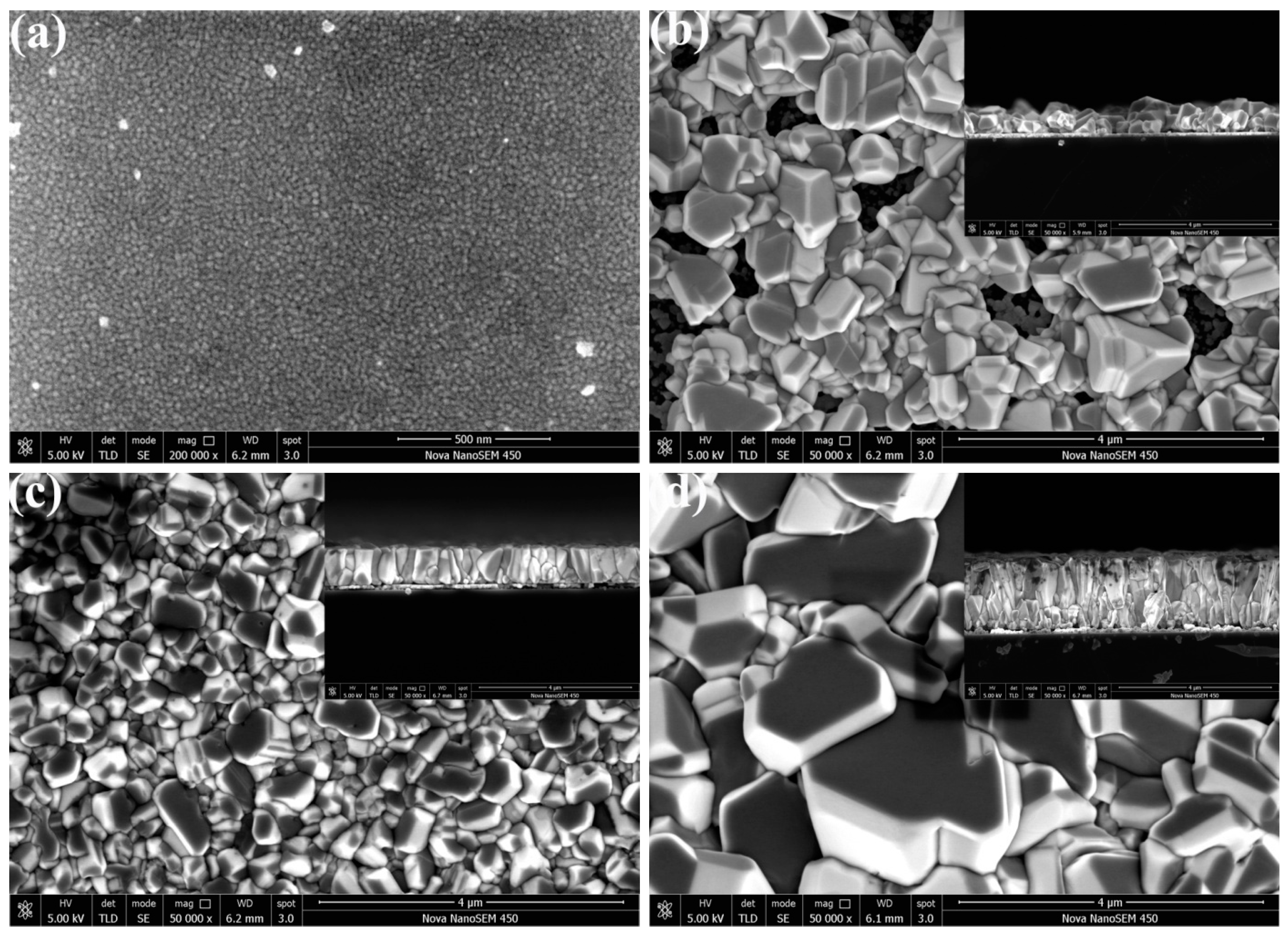
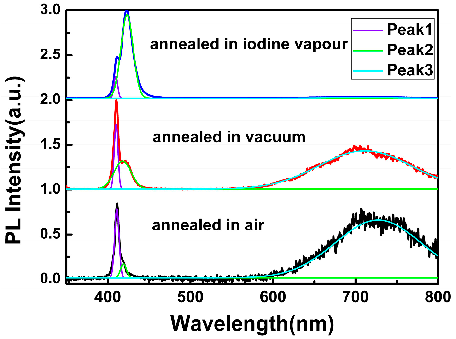
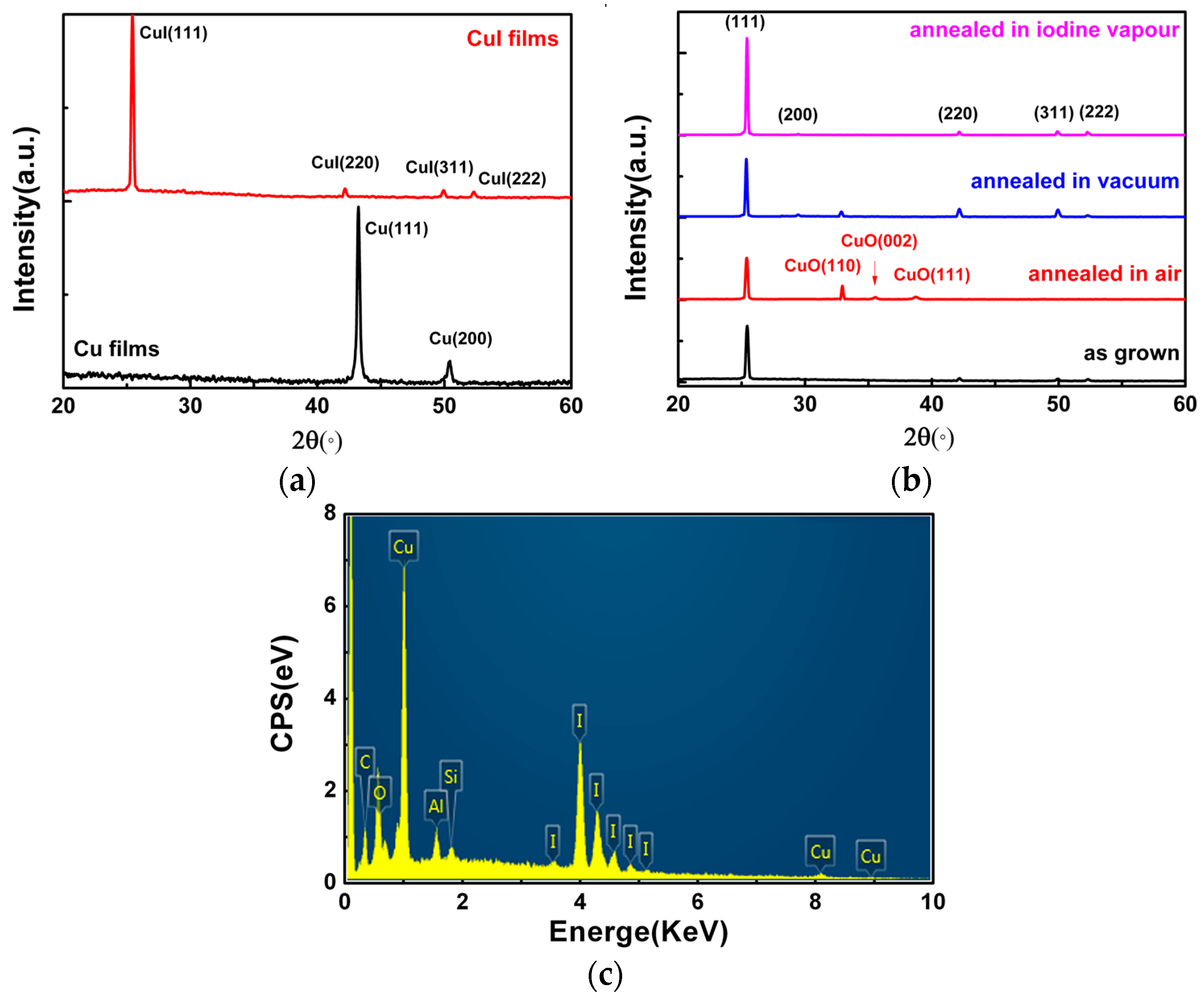
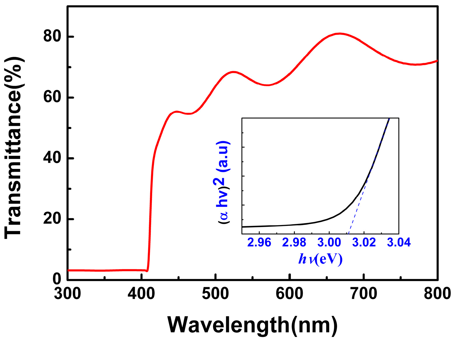
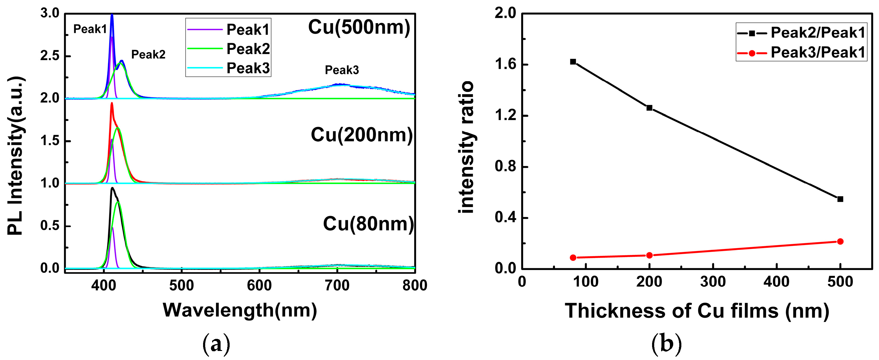
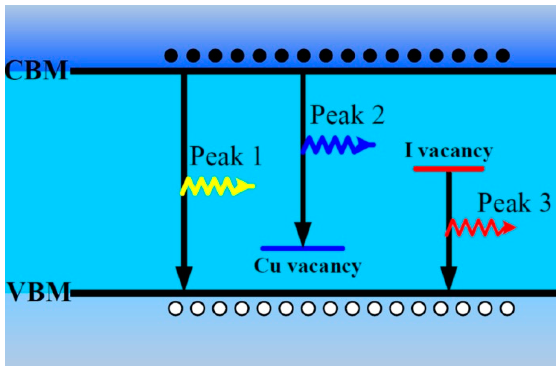
3. Results and Discussion
4. Conclusions
Supplementary Materials
Acknowledgments
Author Contributions
Conflicts of Interest
References
- Grundmann, M.; Schein, F.L.; Lorenz, M.; Böntgen, T.; Lenzner, J.; Wenckstern, H.V. Cuprous iodide: A p-type transparent semiconductor, history, and novel applications. Phys. Status Solidi A 2013, 210, 1671–1703. [Google Scholar] [CrossRef]
- Zhu, B.L.; Zhao, X.Z. Transparent conductive CuI thin films prepared by pulsed laser deposition. Phys. Status Solidi A 2011, 208, 91–96. [Google Scholar] [CrossRef]
- Sankapal, B.R.; Ennaoui, A.; Guminskaya, T.; Dittrich, T.; Bohne, W.; Rohrich, J.; Strub, E.; Lux-Steiner, M.C. Characterization of p-CuI prepared by the SILAR technique on Cu-tape/n-CuInS2 for solar cells. Thin Solid Films 2005, 480, 142–146. [Google Scholar] [CrossRef]
- Cheng, C.H.; Wang, J.; Du, G.T.; Shi, S.H.; Du, Z.J.; Fan, Z.Q.; Bian, J.M.; Wang, M.S. Organic solar cells with remarkable enhanced efficiency by using a CuI buffer to control the molecular orientation and modify the anode. Appl. Phys. Lett. 2010, 97, 083305. [Google Scholar] [CrossRef]
- Lee, J.H.; Leem, D.S.; Kim, H.J.; Kim, J.J. Effectiveness of p-dopants in an organic hole transporting material. Appl. Phys. Lett. 2009, 94, 123306. [Google Scholar] [CrossRef]
- Schein, F.L.; Wenckstern, H.V.; Grundmann, M. Transparent p-CuI/n-ZnO heterojunction diodes. Appl. Phys. Lett. 2013, 102, 092109. [Google Scholar] [CrossRef]
- Ding, K.; Hu, Q.C.; Chen, D.G.; Zheng, Q.H.; Xue, X.G.; Huang, F. Fabrication and Energy Band Alignment of n-ZnO/p-CuI Heterojunction. IEEE Electr. Device Lett. 2012, 33, 1750–1752. [Google Scholar] [CrossRef]
- Yang, C.; Kneiß, M.; Schein, F.L.; Lorenz, M.; Grundmann, M. Room-temperature domain epitaxy of Copper Iodide thin films for transparent CuI/ZnO heterojunctions with high rectification ratios larger than 109. Sci. Rep. 2016, 6, 21937. [Google Scholar] [CrossRef] [PubMed]
- Zheng, Z.; Liu, A.; Wang, S.; Huang, B.; Wong, K.W.; Zhang, X.; Hark, S.K.; Lau, W.M. Growth of highly oriented (110) γ-CuI film with sharp exciton band. J. Mater. Chem. 2008, 18, 852–854. [Google Scholar] [CrossRef]
- Xia, M.; Gu, M.; Liu, X.; Liu, B.; Huang, S.; Ni, C. Luminescence characteristics of CuI film by iodine annealing. J. Mater. Sci. Mater. Electron. 2015, 26, 5092–5096. [Google Scholar] [CrossRef]
- Kosta, I.; Azaceta, E.; Yate, L.; Cabañero, G.; Grande, H.; Tena-Zaera, R. Cathodic electrochemical deposition of CuI from room temperature ionic liquid-based electrolytes. Electrochem. Commun. 2015, 59, 20–23. [Google Scholar] [CrossRef]
- Nejand, B.A.; Ahmadi, V.; Shahverdi, H.R. Growth of plate like γ-CuI nanostructure on copper substrate by hydrothermal evaporation of solution. Mater. Lett. 2014, 132, 138–140. [Google Scholar] [CrossRef]
- Ma, Y.; Gu, M.; Huang, S.; Liu, X.; Liu, B.; Ni, C. Colloidal synthesis of uniform CuI nanoparticles and their size dependent optical properties. Mater. Lett. 2013, 100, 166–169. [Google Scholar] [CrossRef]
- Johan, M.R.; Wen, K.S.; Hawari, N.; Aznan, N.A.K. Synthesis and Characterization of Copper (I) Iodide Nanoparticles via Chemical Route. Int. J. Electrochem. Sci. 2012, 7, 4942–4950. [Google Scholar]
- Sirimanne, P.M.; Rusop, M.; Shirata, T.; Soga, T.; Jimbo, T. Characterization of CuI thin films prepared by different techniques. Mater. Chem. Phys. 2003, 80, 461–465. [Google Scholar] [CrossRef]
- Sirimanne, P.M.; Rusop, M.; Shirata, T.; Soga, T.; Jimbo, T. Characterization of transparent conducting CuI thin films prepared by pulse laser deposition technique. Chem. Phys. Lett. 2002, 366, 485–489. [Google Scholar] [CrossRef]
- Gu, M.; Gao, P.; Liu, X.L.; Huang, S.M.; Liu, B.; Ni, C.; Xu, R.K.; Ning, J. Crystal growth and characterization of CuI single crystals by solvent evaporation technique. Mater. Res. Bull. 2010, 45, 636–639. [Google Scholar] [CrossRef]
- Gruzintsev, A.N.; Zagorodnev, W.N. Effect of Annealing on the Luminescence of p-CuI Crystals. Semiconductors 2012, 46, 149–154. [Google Scholar] [CrossRef]
- Volanti, D.P.; Keyson, D.; Cavalcante, L.S.; Simoes, A.Z.; Joya, M.R.; Longo, E.; Varela, J.A.; Pizani, P.S.; Souza, A.G. Synthesis and characterization of CuO flower-nanostructure processing by a domestic hydrothermal microwave. J. Alloys Compd. 2008, 459, 537–542. [Google Scholar] [CrossRef]
- Perera, V.P.S.; Tennakone, K. Recombination processes in dye-sensitized solid-state solar cells with CuI as the hole collector. Sol. Energy Mater. Sol. Cells 2003, 79, 249–255. [Google Scholar] [CrossRef]
- Yang, Y.; Ga, Q. Growth and photoluminescence characterization of highly oriented CuI/β-Cyclodextrin hybrid composite film. Langmuir 2005, 21, 6866–6871. [Google Scholar] [CrossRef] [PubMed]
- Chen, D.; Wang, Y.; Zhang, L.; Huang, J.; Chen, X.; Pan, D.; Huang, F. Growth strategy and physical properties of the high mobility p-type CuI crystal. Cryst. Growth Des. 2010, 10, 2057–2060. [Google Scholar] [CrossRef]
- Gao, P.; Gu, M.; Liu, X.L.; Liu, B.; Huang, S.M. X-ray excited luminescence of cuprous iodide single crystals: On the nature of red luminescence. Appl. Phys. Lett. 2009, 95, 221904. [Google Scholar] [CrossRef]
- Gao, P.; Gu, M.; Liu, X.; Zheng, Y.Q.; Shi, E.W. Photoluminescence study of annealing effects on CuI crystals grown by evaporation method. Cryst. Res. Technol. 2012, 47, 707–712. [Google Scholar] [CrossRef]
- Meng, L.; Mo, R.; Zhou, H.; Wang, G.; Chen, W.; Wang, D.; Peng, Q. Synthesis of luminescent cubic phase one-dimensional CuI nanostructures in solution. Cryst. Growth Des. 2010, 10, 3387–3390. [Google Scholar] [CrossRef]


| Sample (Annealing Treatment) | FWHM of Peak 1 | Ipeak2/Ipeak1 | Ipeak3/Ipeak1 |
|---|---|---|---|
| as-grown | 5.586 | 1.262 | 0.106 |
| Air | 6.361 | 0.219 | 0.859 |
| vacuum | 5.366 | 0.438 | 0.598 |
| iodine vapor | 5.243 | 3.582 | 0.008 |
© 2016 by the authors; licensee MDPI, Basel, Switzerland. This article is an open access article distributed under the terms and conditions of the Creative Commons Attribution (CC-BY) license (http://creativecommons.org/licenses/by/4.0/).
Share and Cite
Lin, G.; Zhao, F.; Zhao, Y.; Zhang, D.; Yang, L.; Xue, X.; Wang, X.; Qu, C.; Li, Q.; Zhang, L. Luminescence Properties and Mechanisms of CuI Thin Films Fabricated by Vapor Iodization of Copper Films. Materials 2016, 9, 990. https://doi.org/10.3390/ma9120990
Lin G, Zhao F, Zhao Y, Zhang D, Yang L, Xue X, Wang X, Qu C, Li Q, Zhang L. Luminescence Properties and Mechanisms of CuI Thin Films Fabricated by Vapor Iodization of Copper Films. Materials. 2016; 9(12):990. https://doi.org/10.3390/ma9120990
Chicago/Turabian StyleLin, Guochen, Fengzhou Zhao, Yuan Zhao, Dengying Zhang, Lixin Yang, Xiaoe Xue, Xiaohui Wang, Chong Qu, Qingshan Li, and Lichun Zhang. 2016. "Luminescence Properties and Mechanisms of CuI Thin Films Fabricated by Vapor Iodization of Copper Films" Materials 9, no. 12: 990. https://doi.org/10.3390/ma9120990
APA StyleLin, G., Zhao, F., Zhao, Y., Zhang, D., Yang, L., Xue, X., Wang, X., Qu, C., Li, Q., & Zhang, L. (2016). Luminescence Properties and Mechanisms of CuI Thin Films Fabricated by Vapor Iodization of Copper Films. Materials, 9(12), 990. https://doi.org/10.3390/ma9120990