Article

One-Step Formation of WO3-Loaded TiO2 Nanotubes Composite Film for High Photocatalytic Performance

Nanotechnology & Catalysis Research Centre (NANOCAT), Institute of Postgraduate Studies (IPS), University of Malaya, Kuala Lumpur 50603, Malaysia
*
Author to whom correspondence should be addressed.
These authors contributed equally to this work.
Materials 2015, 8(5), 2139-2153; https://doi.org/10.3390/ma8052139
Submission received: 12 November 2014 / Revised: 19 March 2015 / Accepted: 20 March 2015 / Published: 27 April 2015
(This article belongs to the Special Issue Photocatalytic Materials)

Abstract

:
High aspect ratio of WO3-loaded TiO2 nanotube arrays have been successfully synthesized using the electrochemical anodization method in an ethylene glycol electrolyte containing 0.5 wt% ammonium fluoride in a range of applied voltage of 10–40 V for 30 min. The novelty of this research works in the one-step formation of WO3-loaded TiO2 nanotube arrays composite film by using tungsten as the cathode material instead of the conventionally used platinum electrode. As compared with platinum, tungsten metal has lower stability, forming dissolved ions (W6+) in the electrolyte. The W6+ ions then move towards the titanium foil and form a coherent deposit on titanium foil. By controlling the oxidation rate and chemical dissolution rate of TiO2 during the electrochemical anodization, the nanotubular structure of TiO2 film could be achieved. In the present study, nanotube arrays were characterized using FESEM, EDAX, XRD, as well as Raman spectroscopy. Based on the results obtained, nanotube arrays with average pore diameter of up to 74 nm and length of 1.6 µm were produced. EDAX confirmed the presence of tungsten element within the nanotube arrays which varied in content from 1.06 at% to 3.29 at%. The photocatalytic activity of the nanotube arrays was then investigated using methyl orange degradation under TUV 96W UV-B Germicidal light irradiation. The nanotube with the highest aspect ratio, geometric surface area factor and at% of tungsten exhibited the highest photocatalytic activity due to more photo-induced electron-hole pairs generated by the larger surface area and because WO3 improves charge separation, reduces charge carrier recombination and increases charge carrier lifetime via accumulation of electrons and holes in the two different metal oxide semiconductor components.

1. Introduction

The process of dyeing in the textile industry has resulted in the production of large amounts of wastewater with intense coloration which has to be eliminated before release into natural water streams. If left untreated, such dyes will remain in the environment for an extended period of time and cause serious environmental and health problems. Therefore, such compounds must be completely removed from aquatic system [1,2].
Titanium dioxide (TiO2) is one of the most widely studied transition metal oxide semiconductor and has been widely applied in solar cells, hydrogen generation, gas sensing, and photocatalysis applications [3,4,5]. One of the most widely researched and an important application of TiO2 photocatalyst is pollution treatment. The effectiveness of TiO2 in these applications is further complimented by its unique properties of non-toxicity, cost effective, long-term stability, widespread availability, corrosion stability, and high photocatalytic ability. However, researchers have shown that TiO2 nanotubes are only able to utilize around 2%–3% solar light that reaches the earth due to a large band gap of 3.20 eV [6]. Therefore, the doping of TiO2 nanostructures with transition metals to enable the TiO2 nanostructures to react to a much larger visible region is currently widely researched.
In this present study, tungsten trioxide (WO3) was selected as potential dopant to decorate the pure TiO2 nanotubes. The reason is mainly attributed to the WO3 with a smaller band gap of 2.3–2.8 eV (440 to 540 nm), which is advantageous for visible-light-driven photocatalysis [7]. Furthermore, the upper edge of the valence band and the lower edge of the conduction band are lower for WO3 than for TiO2. These differences in band edge positions create a potential gradient at the composite interface. This facilitates better charge separation and inhibits charge carrier recombination. Also, the properties and performance of the nanotubes are highly dependent on the dimensions of the nanotubes [8,9,10]. To optimize the properties and performance of the nanotubes, anodizing conditions such as applied potential, anodization time, and electrolyte composition can be tailored to control the dimensions of the nanotubes such as length, pore diameter and wall thickness [11,12,13,14,15]. The morphology and structure of the nanotubes layer are affected strongly by the electrochemical conditions, especially the anodization voltage, as it is the key factor controlling the tube diameter. Generally, nanotubes growth occurs proportional to the applied potential up to a voltage where dielectric breakdown of the oxide occurs [16]. Tube diameter is affected by voltage but it is not affected by time. Instead, the time of anodization influences the thickness of the nanotube layer [17]. Thus, the influence of anodization voltage on the formation of WO3-loaded TiO2 nanotube arrays was investigated in this study with the aim to fabricate nanotubes with optimum length, wall thickness, and pore diameter for better photocatalysis application. The nanotube diameter is expected to increase with increasing voltage due to higher field assisted oxidation rate of Ti metal to form TiO2 layer and field assisted dissolution rate of Ti metal ions in the electrolyte [18].

2. Results and Discussion

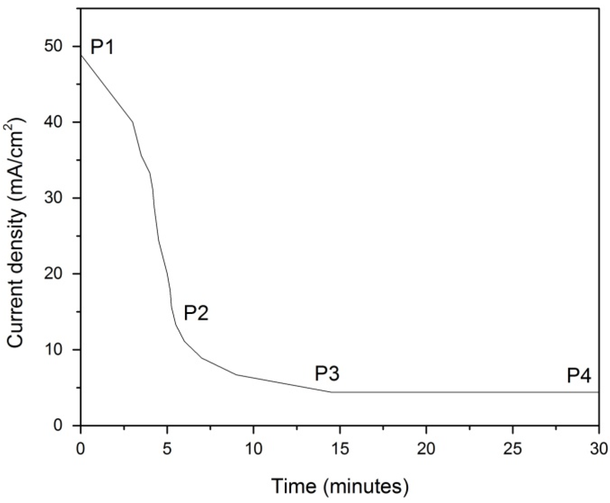
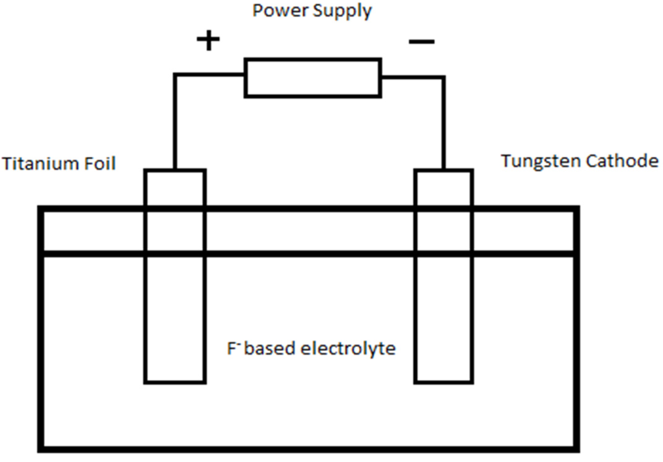
2.1. Transient and Steady State Current Density Analysis

Figure 1 shows the current density curve for a WO3-loaded TiO2 nanotubes sample produced at 40 V and anodized for 30 min in electrolyte containing 0.5 g NH4F. About 5 min after application of the voltage, the measured current density reduced from about 49 mA/cm2 to around 15 mA/cm2, point P2 on the plot. The reduced current density resulted from the field-assisted oxidation of the Ti metal surface, which forms a compact oxide layer [18,19]. The reaction occurred is represented by the equation below:
Ti2+ + H2O2 → TiO2 + 2H+
Figure 1. Anodization current behavior of tungsten trioxide (WO3)-loaded titanium dioxide (TiO2).
Materials 08 02139 g001
Region P2 to P3 represents the field-assisted dissolution of the oxide layer caused by high electric field across the thin layer. The current gradually drops with a corresponding increase in porous structure depth. Fine pits or cracks form on the oxide surfaces which arise from chemical and field-assisted dissolution of the oxide at local points of high energy. The reduced oxide layer thickness at these points decreases the current density [18,20,21]. The equation below represents the reaction that occurred:
TiO2 + 4H+ + 6F → [TiF6]2 + 2H2O
Point P3 shows the transition between the porous and nanotube structures. Nanotube array length increases to point P4 after which the current is cut off and the reaction is ended.
The current density curves for experiments conducted at 10 V, 20 V and 30 V are not plotted since they follow the same path as the 40 V experiment (within reasonable error). The formation of WO3-loaded TiO2 nanotubes is illustrated in Figure 2.
Figure 2. Formation of WO3-loaded TiO2 nanotubes: (a) Ti foil; (b) oxide layer formation; (c) chemical dissolution of oxide layer and (d) titania nanotubes.
Materials 08 02139 g002
The equation below represents the formation of WO3 species for the synthesis of anodic WO3-loaded TiO2 nanostructure:
W6+ + 3H2O → WO3 + 6H+

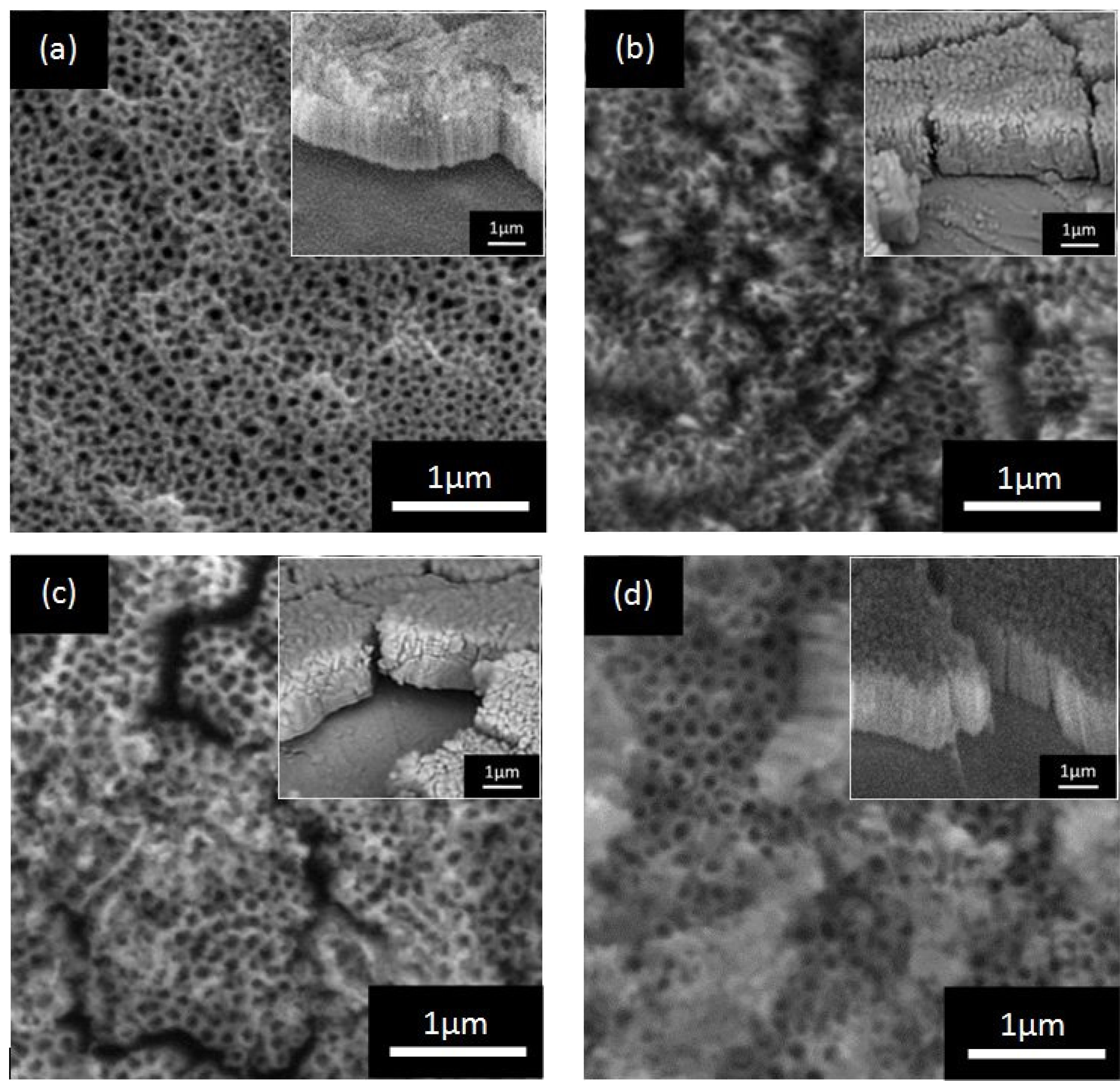
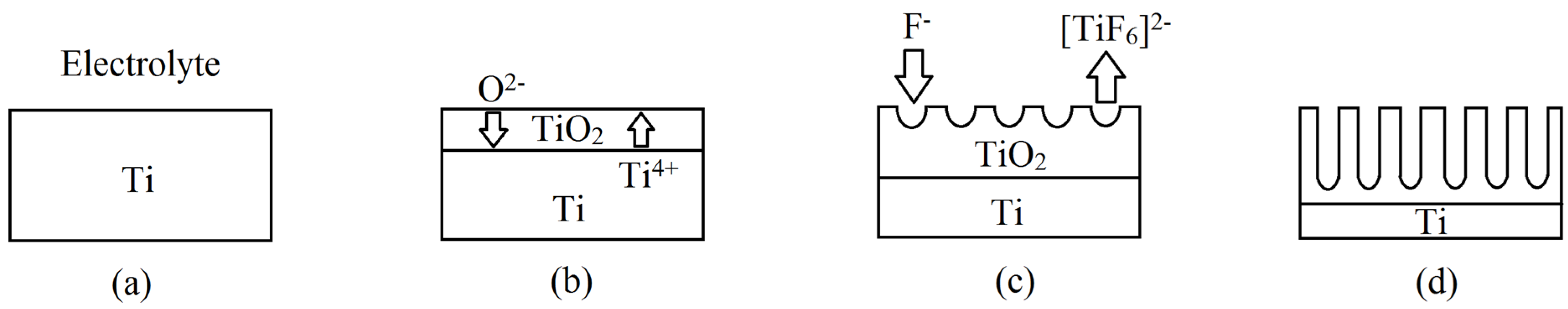
2.2. Morphological Studies and Elemental Analysis

The effect of anodization voltage on the morphology of anodic WO3-loaded TiO2 nanostructure was investigated. Figure 3 showed the surface morphologies of anodic WO3-loaded TiO2 layer of different anodization voltage from 10 V to 40 V. All samples were anodized for 30 min in electrolyte composed of EG, NH4F and H2O2. Anodization voltage of 10 V produced nanotube arrays with smallest average pore’s diameter of 47 nm and shortest length of approximately 0.9 µm. At anodization voltage of 20 V, nanotube arrays with average pore’s diameter of 56 nm and length of approximately 1.2 µm were produced. As anodization voltage is increased to 30 V, the average pore’s diameter and length of the nanotube arrays also increased to 65 nm and 1.4 µm respectively. Anodization voltage of 40 V produced nanotube arrays with the longest tube length of approximately 1.6 μm and largest average pore’s size of 74 nm. The average diameter, length, wall thickness, aspect ratio (AR), and geometric surface area factor (G) of the nanotubes anodized at different applied voltage are summarized in Table 1. The aspect ratio and geometric area factor were calculated as follows:
AR = L/(D + 2w)
G = [4πL (D + w)]/[√3 (D + 2w)2] + 1
where L = nanotube length in nm; D = pore size; w = wall thickness.
The diameter and length of nanotubes were found to increase with anodization voltage up to 40 V because of the high electric field dissolution at the barrier layer of nanotubes [18]. At low potential (10 V), the low field assisted oxidation rate and field-assisted dissolution rate during the anodization process resulted in small diameter of pores. Thus, short and small nanotubular structures were formed. However, at higher potential, these small nanotubular structures were then etched into larger pores due to the higher field assisted oxidation and dissolution rate. Higher voltage will provide higher driving force for ionic species (H+, F, and O2) to move through the barrier layer at the bottom of the nanotube, which allows for faster movement of the Ti/TiO2 interface into the Ti metal [18,22]. Nanotube arrays with longer length will be produced from this improved pore deepening process.
Figure 3. Field emission scanning electron microscopy (FESEM) images of WO3-loaded TiO2 nanotubes obtained for different anodization voltage at: (a) 10 V; (b) 20 V; (c) 30 V and (d) 40 V. Insets are the side views of the samples.
Materials 08 02139 g003
Table 1. Pore’s diameter, length, wall thickness, aspect ratio, and geometric surface area factor of WO3-loaded TiO2 nanotubes formed with varying anodizing voltage.
Voltage (V)Diameter (nm)Length (µm)Wall Thickness (nm)ARG
10470.91312.3374.52
20561.21513.9584.58
30651.41714.1485.98
40741.61814.5589.26
The quantitative elemental analysis of WO3-loaded TiO2 nanotubes was carried out by FESEM-EDAX and the average elemental compositions (at%) were obtained by taking eight spots in EDAX analysis. The percentage of each element is shown in Table 2. The WO3-loaded TiO2 nanotubes show the presence of Ti, O, W and C elements. Sample anodized at 40 V shows the highest at% of W which is 3.29 at%. The samples anodized at 30 V and 20 V showed 2.01 at% and 1.36 at% of W, respectively. The sample anodized at 10 V showed the lowest at% of W which is 1.06 at%. The presence of W within the nanotube arrays was found to increase with anodization voltage. This is because increasing voltage will increase the strength of electric field in the electrolyte solution, thereby increasing the mobility and rate of migration of W6+ ions towards the titanium foil [23]. Therefore, at higher anodization voltage, more W will be incorporated into the TiO2 nanotubes.
Table 2. Energy-dispersive X-ray elemental analysis of WO3-loaded TiO2 nanotubes.
SamplesAtomic %
TiOWC
10 V43.8151.791.063.34
20 V48.1646.951.363.53
30 V59.2231.832.016.94
40 V47.3844.113.295.22

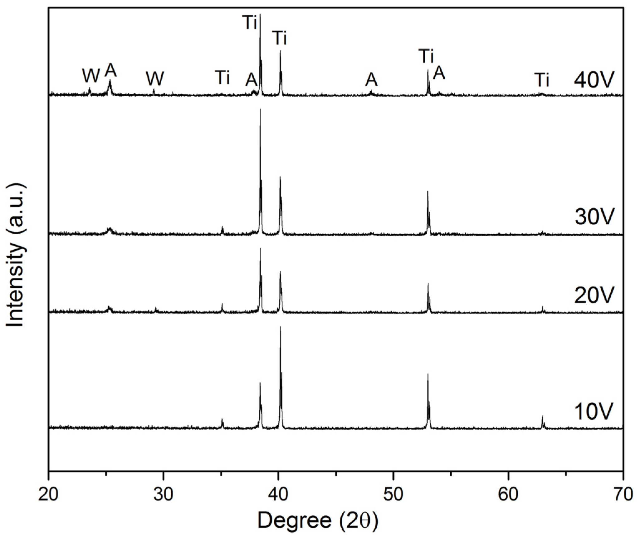
2.3. Phase Structure Analysis
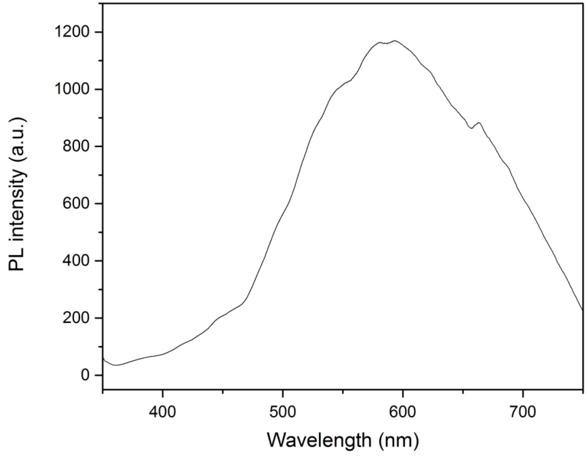
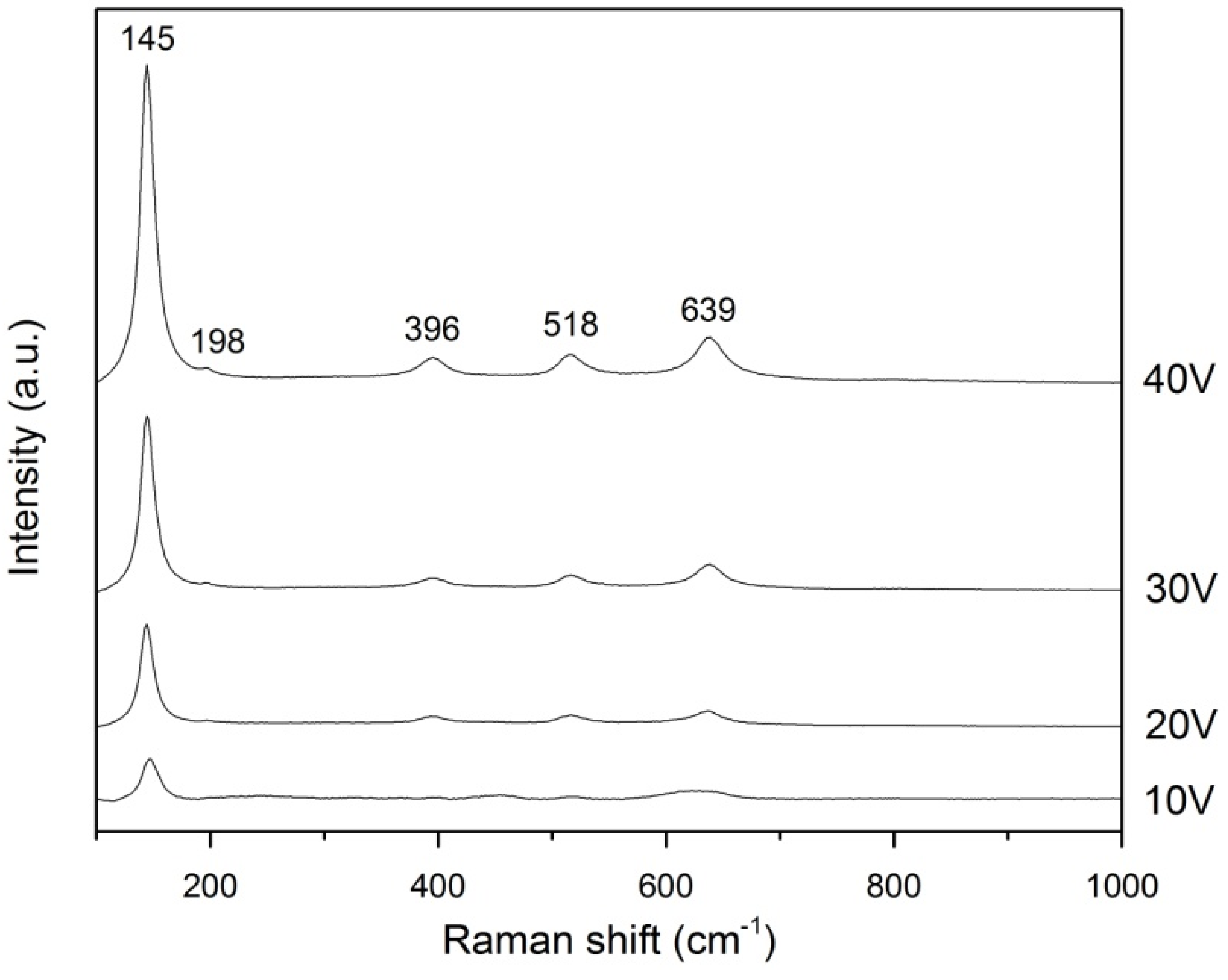
Figure 4 is an XRD profile of the WO3-loaded TiO2 nanotubes after annealing at 400 °C in air atmosphere for 4 h. The result shows the presence of TiO2 with anatase phase [JCPDS No. 21-1272]. The diffraction peaks at 25.37°, 38.67°, 48.21°, and 54.10° are corresponding to (101), (112), (200), and (105) crystal planes for the anatase phase, respectively. Additionally, for the sample synthesized at 40 V, small additional peaks at 23.62° and 29.16° corresponds with the (020) and (120) crystal planes of the monoclinic WO3 phase. The intensity of the (101) peak at 25.37° increased with increasing anodization voltage, indicating the increased crystallinity of anatase phase. This increase in anatase intensity is due to more growth of TiO2 nanotubes as voltage is further increased. Furthermore, TiO2 layer formed at higher voltages are thicker and denser, resulting in higher anatase intensity [24]. However, the XRD patterns did not show any obvious WO3 phase for samples synthesized at 10 V, 20 V and 30 V. A possible explanation would be that the XRD analysis was not sensitive enough to detect very low WO3 content (<3 at% from EDX analysis) within the TiO2 lattice due to the nearly similar ionic radius of W6+ and Ti4+ [25,26].
Figure 4. X-ray diffraction patterns of WO3-loaded TiO2 nanotubes produced at different anodization voltage.
Materials 08 02139 g004

2.4. Raman Analysis

Raman analysis was conducted to detect the presence of WO3 and to confirm the XRD inferences of WO3-loaded TiO2 nanotubes. Figure 5 is the Raman spectrums obtained which shows five characteristic modes at 146, 198, 396, 516, and 640 cm−1. The mode at 146 cm−1 is strong and assigned as the Eg phonon of the anatase structure and B1g phonon of the rutile structure. The latter four modes are assigned as Eg, B1g, B1g, and Eg modes of the anatase phase, respectively. The positions and intensities of the five Raman active modes correspond well with the anatase phase of TiO2 [27,28,29]. The Raman spectrums show increasing intensity of peaks from 10 V to 40 V. Higher intensity of peaks corresponds to higher crystallinity [29]. The increase in anatase intensity from 10 V to 40 V is due to more growth of TiO2 nanotubes as voltage is increased. Furthermore, TiO2 layer formed at higher voltages are thicker and denser, resulting in higher anatase intensity [19]. However, Raman bands for WO3 was not detected because typical characteristic modes for WO3 are similar to those for anatase (e.g., 327, 714, and 804 cm−1) and were overlapped by bands for the anatase phase [30].
Figure 5. Raman spectrum of WO3-loaded TiO2 produced at different anodization voltage.
Materials 08 02139 g005

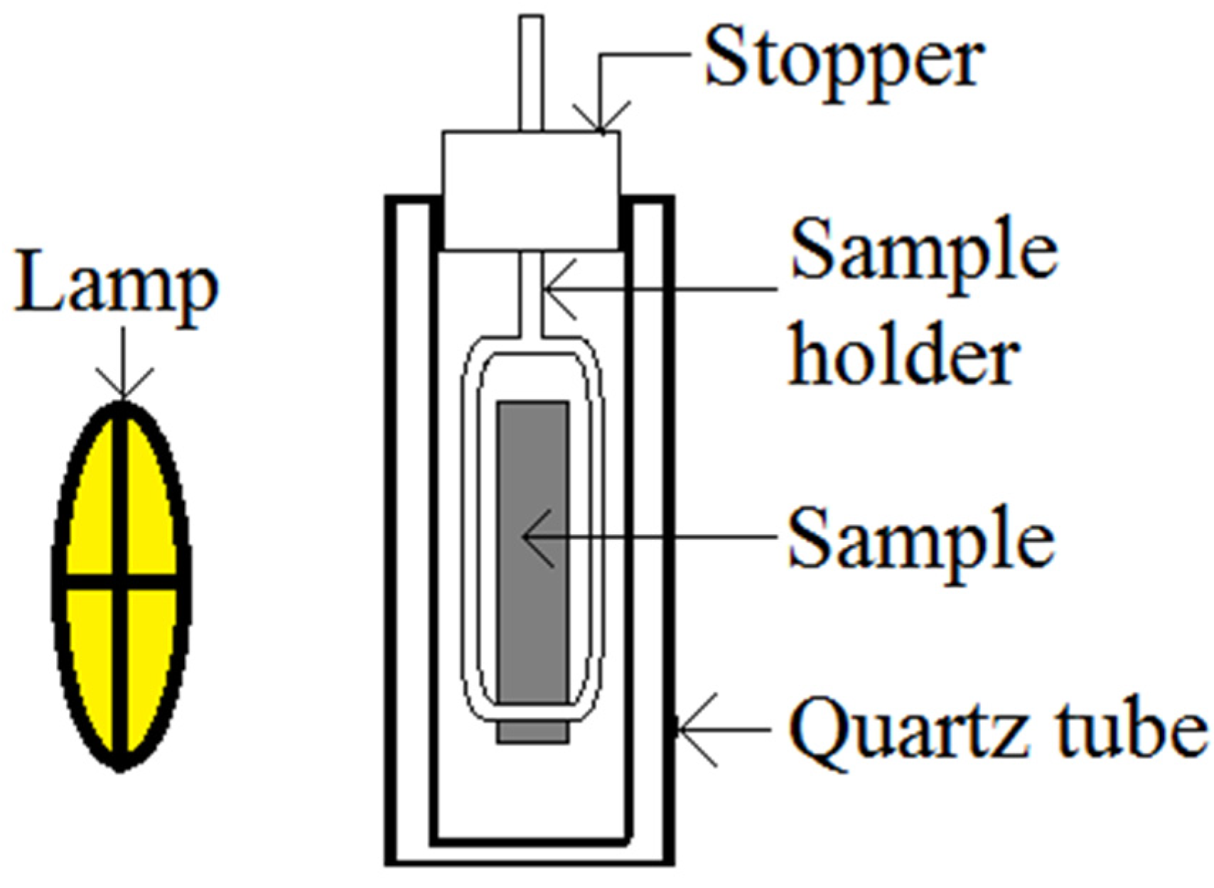
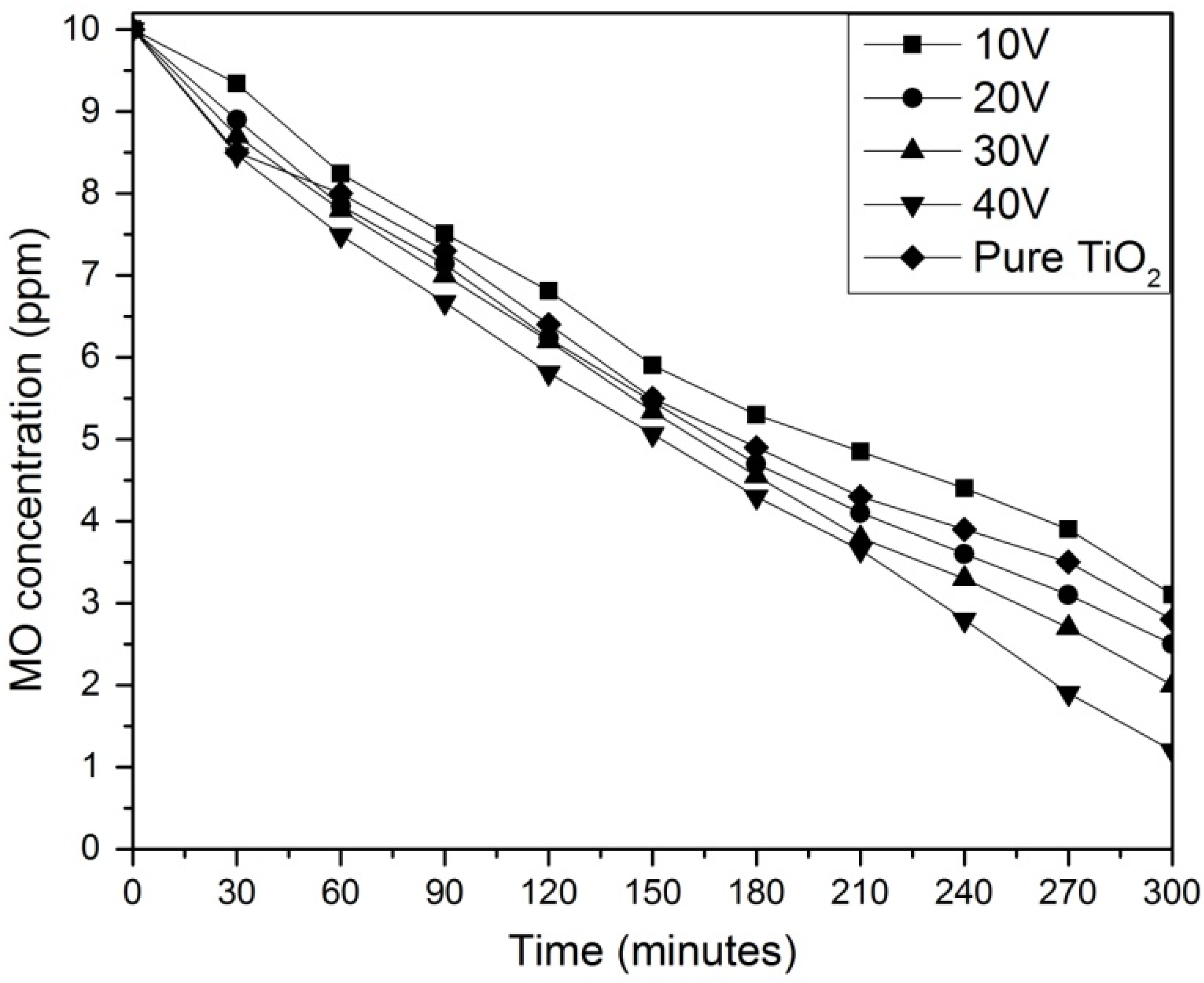
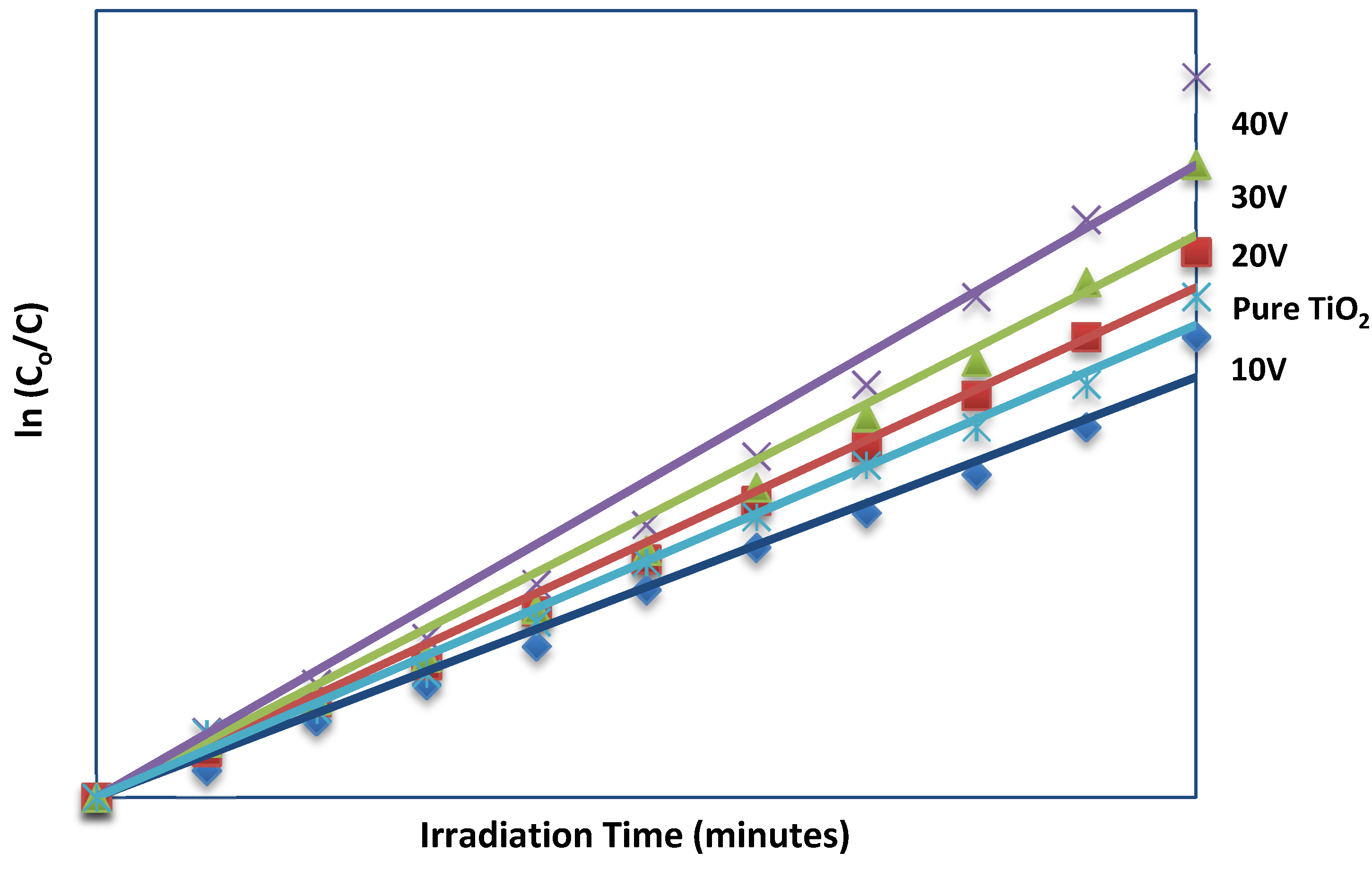
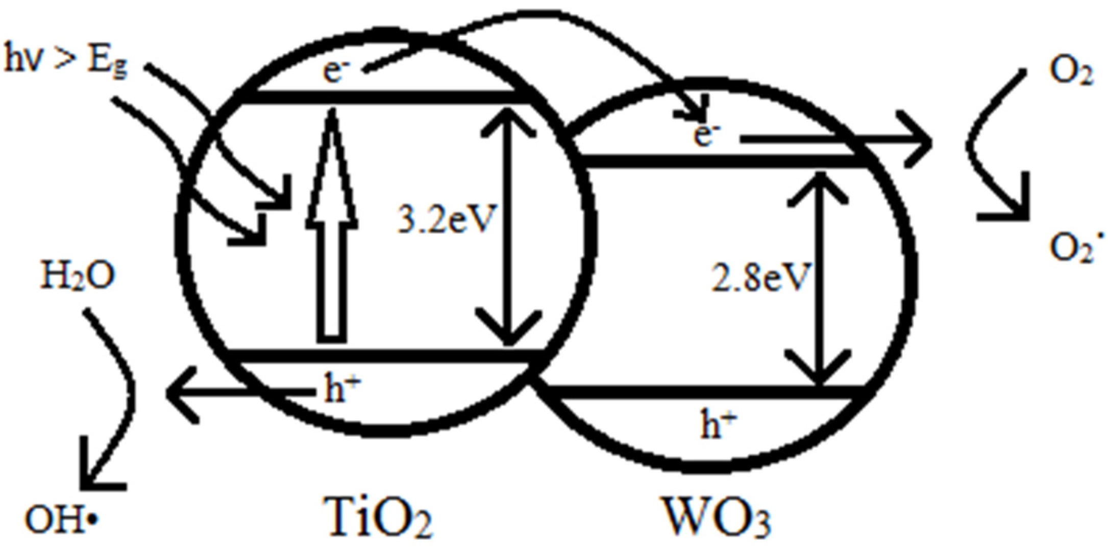
2.5. Photocatalytic Activity

The photocatalytic ability of the WO3-loaded TiO2 nanotube arrays was tested through the MO degradation under UV light irradiation. As shown in Figure 6, the nanotube arrays produced at 40 V presented the highest degradation percentages for the decomposition of MO where only 12% of initial MO concentration remained after 4 h of UV irradiation. Nanotube arrays produced at 30 V and 20 V showed lower efficiency of MO decomposition, where the MO concentration was reduced to 20% and 25% respectively. The sample anodized at 10 V showed the lowest activity, where the MO concentration was only reduced to 31% of initial MO concentration. WO3-loaded TiO2 nanotube arrays anodized at 40 V having the highest aspect ratio and geometric surface area factor exhibited the highest photocatalytic activity among the samples due to the larger active surface area to generate more photo-induced electron-hole pairs. The photoresponse of the WO3-loaded TiO2 nanotubes is affected by the nanotubes’ length where longer tubes provide higher total light absorption. Also, with the larger surface area, more reactants can be adsorbed onto the inner and outer TiO2 nanotube surfaces and thus result in higher photocatalytic activity [3,11]. In order to compare the photocatalytic activity of WO3-loaded TiO2 nanotubes with pure TiO2 nanotubes, pure TiO2 nanotubes were produced using the same parameters as the WO3-loaded TiO2 nanotubes anodized at 40 V except replacing the tungsten cathode with a platinum cathode. As compared to WO3-loaded TiO2 nanotubes, pure TiO2 nanotube arrays showed a lower efficiency of MO decomposition, where the MO concentration was reduced to 28% of initial MO concentration after 4 h. This shows that the coupling of WO3 and TiO2 gives significant improvement in the photocatalytic activity of the nanotube arrays due to suppression of the recombination of the photogenerated carriers and increased charge separation of TiO2 [31,32,33].
Figure 6. Photodegradation of methyl orange (MO) solution by WO3-loaded TiO2 nanotubes anodized at different voltage.
Materials 08 02139 g006
The kinetics analysis of MO degradation is illustrated in Figure 7. The linear curves suggests that the photocatalytic degradation of MO can be described by the first order kinetic model, ln (C0/C) = kt, where C0 is the initial concentration and C is the concentration at time t. The plots of the concentration data gave a straight line. The results of fitting experimental data to pseudo-first-order kinetics are given in Table 3. The rate constant increases with increasing anodization voltage. This shows that the WO3-loaded TiO2 nanotubes anodized at 40 V demonstrated the best photocatalytic activity for the degradation of MO among the samples produced.
Figure 7. Pseudo-first-order kinetics for methyl orange photodegradation using WO3-loaded TiO2 nanotubes anodized at different voltage and pure TiO2 nanotubes.
Materials 08 02139 g007
Table 3. Rate constants for catalytic photodegradation of MO.
SamplesRate Constant (k)R2
10 V0.00360.9874
20 V0.00430.9920
30 V0.00480.9759
40 V0.00540.9715
Pure TiO20.00400.9927
Figure 8 shows the energy band diagram of TiO2 and WO3. As shown in Figure 9, UV light radiation excites electrons from the valence band to the conduction band which results in electrons and holes separation. When the electrons and holes reach the semiconductor-environment interface, they will react with appropriate redox species (H2O and O2) to form reactive intermediates (OH• and O2•). These radicals and photogenerated holes are extremely strong oxidants which are able to oxidize all organic materials to CO2 and H2O, leading to the degradation of MO solution [3]. The coupling of TiO2 and WO3 can lead to electron and hole transfer from one semiconductor particle to another upon light excitation [31]. The valence and conduction band potentials of TiO2 are more cathodic than that of WO3. Thus, photogenerated electrons can transfer from the conduction band of TiO2 down to the conduction band of WO3. This suppresses the recombination of the photogenerated carriers, leading to increased photo-oxidation efficiency [32]. The lower band gap of WO3 also increases the charge separation of TiO2 and extends the energy range of photoexcitation of the system. If a photon with not enough energy to excite TiO2 but is of enough energy to excite WO3 is incident, the hole that is created in the WO3 valence band is excited to the conduction band of TiO2, while the electron is transferred to the conduction band of TiO2. It is this electron transfer that increases the charge separation and increases the efficiency of the photocatalytic process [33].
Figure 8. Energy band diagram of TiO2 and WO3.
Materials 08 02139 g008
Figure 9. Photocatalytic mechanism of WO3-loaded TiO2 under UV light irradiation.
Materials 08 02139 g009

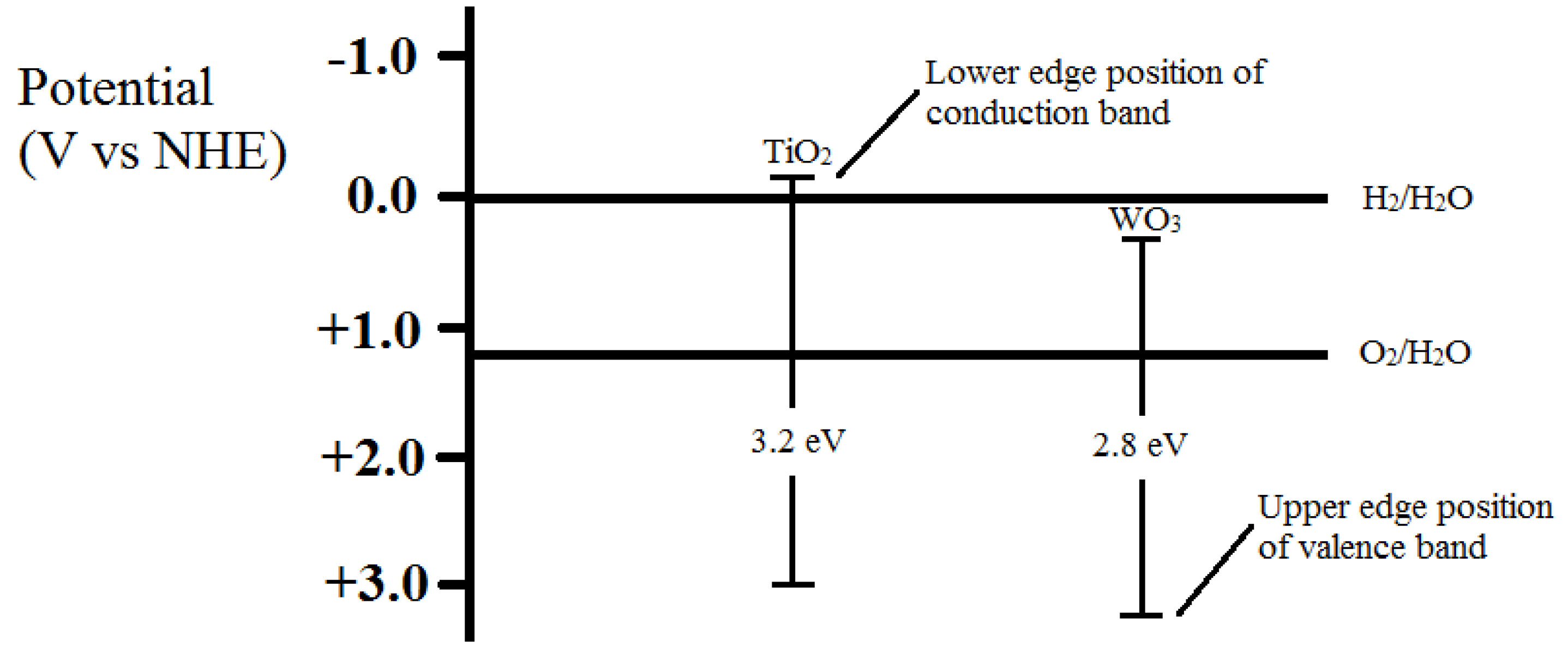
2.6. Optical Properties Analysis

The determination of the energy band gap of the WO3-loaded TiO2 nanotubes is a key point for application purpose. To investigate the optical properties of the WO3-loaded TiO2 nanotubes, we have performed photoluminescence (PL) analysis on the sample that showed the best performance in the photocatalytic activity test. The PL emission spectrum is a useful characterization tool which can be used to test the opticl properties of the nanocomposite. The band gap energy (Ebg) of the sample is calculated as follows: Ebg = hc/λ, where Ebg is the band gap energy, h is Planck’s constant (4.135667 × 10⁻¹⁵ eVs), c is the velocity of light (2.997924 × 10⁸ m/s), and λ is the wavelength (nm) of PL emission. In the photoluminescence spectra, the wavelength corresponding to the highest PL emission intensity is the light wavelength at which the sample is most active. By taking this wavelength value as λ, the energy band gap of the sample can be estimated. Figure 10 shows the photoluminescence spectra for WO3-loaded TiO2 nanotubes anodized at 40 V. From this photoluminescence spectrum, the sample shows the highest PL emission intensity at wavelength of 580 nm. By taking this wavelength into account, we estimate the energy band gap of the sample to be 2.14 eV. This band gap value is much lower than that of WO3 alone (2.8 eV), attributed to the presence of carbon species within the TiO2 nanotubes. Previous studies have also shown that carbon can be doped onto TiO2 nanotubes from organic electrolyte such as ethylene glycol during anodization [34,35,36]. The presence of carbon significantly enhanced the visible light responsiveness of the WO3-loaded TiO2 nanotubes because the mixing of the delocalized p state of the carbon dopants with O 2p orbital in valence band of TiO2 will shift the valence band edge of TiO2 upwards, thus narrowing down the band gap energy of TiO2.
Figure 10. Smooth photoluminescence (PL) curve for WO3-loaded TiO2 nanotubes anodized at 40 V.
Materials 08 02139 g010

3. Experimental Section

The experiments were carried out in a two electrodes electrochemical cell as shown in Figure 11, where the two electrodes were placed 2 cm apart. Titanium (Ti) foil (0.127 mm, purity 99.6%, Sigma Aldrich, St. Louis, MO, USA) (5 cm × 1 cm dimension) over which WO3-loaded TiO2 nanotubes were grown was used as anode while tungsten foil (0.127 mm, purity 99.9%, Sigma Aldrich, St. Louis, MO, USA) was the counter electrode. The electrolytes were 0.5 wt% ammonium fluoride (NH4F, Merck, Kenilworth, NJ, USA) dissolved in anhydrous ethylene glycol (EG, Friendemann Schmidt, Germany) and hydrogen peroxide (H2O2, Friendemann Schmidt, Germany). The function of H2O2 is to replace H2O as oxygen provider to increase the oxidation rate for synthesizing highly ordered and smooth TiO2 nanotubes at a rapid rate [37]. Anodization was carried out in a range of anodization voltage of 10–40 V. The anodization period was restricted to only 30 min, which was a typical time observed for growth of 1 µm long TiO2 nanotubes [3,4]. As-anodized anodic WO3-loaded TiO2 samples were cleaned using deionized water followed by sonication in acetone (Friendemann Schmidt, Germany) to remove the remaining occluded ions from the anodized solutions or barrier oxide layer. The samples were then subjected to calcination at 400 °C for 4 h in air atmosphere.
Figure 11. Schematic drawing of an electrochemical cell in which the Ti electrode is anodized.
Materials 08 02139 g011
The morphologies of anodic WO3-loaded TiO2 nanostructures were observed by field emission scanning electron microscopy (FESEM, FEI Quanta 200F Environmental SEM with EDAX, Hillsboro, OR, USA) microanalysis at 5 kV. The structural variations measurement and phase determination were done using X-ray diffraction (XRD, Bruker D8 Advance diffractometer, Billerica, MA, USA) analysis conducted from 10 to 80 with Cu Kα radiation (α = 1.5406 Å). The phase composition was determined using Raman Spectroscopy (Renishaw inVia, Renishaw plc, Gloucestershire, UK) with a 514.5 nm Ar+ laser as an excitation source.
Photocatalytic degradation studies were performed by dipping sintered sample in 100 mL of 10 ppm methyl orange (MO) solution in a photoreactor consisting of quartz glass, as shown in Figure 12. After leaving the samples in the reactor for 30 min in dark environment for dark adsorption, the samples were photoirradiated at room temperature by using TUV 96W UV-B Germicidal light. To monitor the degradation of methyl orange (MO) after UV irradiation, 5 mL solution was withdrawn from quartz tubes for every 30 min. A UV spectrometer was used to measure the concentration of the degraded MO solution.
Figure 12. Schematic diagram of photocatalytic reactor in which photocatalytic degradation was performed.
Materials 08 02139 g012

4. Conclusions

In this study, the effect of anodization voltage on the formation of WO3-loaded TiO2 nanotube arrays using single step anodization was performed. WO3-loaded TiO2 nanotube arrays were successfully produced at 10 V, 20 V, 30 V and 40 V. The nanotube arrays anodized at 40 V produced the largest pore’s size (74 nm) and longest tube length (1.6 µm). Besides that, the amount of tungsten in the nanotube arrays increased with anodization voltage up to maximum of 3.29 at%. Clearly, WO3-loaded TiO2 nanotube arrays with the highest aspect ratio, geometric surface area factor and at% of tungsten exhibited the more favorable photocatalytic degradation of MO dye under UV light irradiation due to the larger active surface area to generate more photo-induced electron-hole pairs, better charge separation and less charge carrier recombination.

Acknowledgments

The authors would like to thank University of Malaya for funding this research work under University of Malaya Research Grant (UMRG), (RP022-2012D) and Fundamental Research Grant Scheme (FRGS), (FP055-2013B).

Author Contributions

Wai Hong Lee and Chin Wei Lai designed the experiments. Wai Hong Lee carried out the anodization and sample preparations. Wai Hong Lee, Chin Wei Lai and Sharifah Bee Abd Hamid carried out analysis of FESEM-EDAX, XRD, Raman, photoluminescence and UV spectrometer data. Wai Hong Lee, Chin Wei Lai and Sharifah Bee Abd Hamid prepared the manuscript.

Conflicts of Interest

The authors declare no conflict of interest.

References

  1. Olukanni, O.D.; Osuntoki, A.A.; Gbenle, G.O. Textile effluent biodegradation potentials of textile effluent-adapted and non-adapted bacteria. Afr. J. Biotechnol. 2006, 5, 1980–1984. [Google Scholar]
  2. Palamthodi, S.; Patil, D.; Patil, Y. Microbial degradation of textile industrial effluents. Afr. J. Biotechnol. 2013, 10, 12657–12661. [Google Scholar]
  3. Roy, P.; Berger, S.; Schmuki, P. TiO2 nanotubes: Synthesis and applications. Angew. Chem. Int. Ed. 2011, 50, 2904–2939. [Google Scholar] [CrossRef]
  4. Mohapatra, S.; Misra, M.; Mahajan, V.K.; Raja, K.S. A novel method for the synthesis of titania nanotubes using sonoelectrochemical method and its application for photoelectrochemical splitting of water. J. Catal. 2007, 246, 362–369. [Google Scholar] [CrossRef]
  5. Liao, J.Y.; Lei, B.X.; Wang, Y.F.; Liu, J.M.; Su, C.Y.; Kuang, D.B. Hydrothermal fabrication of quasi-one-dimensional single-crystalline anatase TiO2 nanostructures on FTO glass and their applications in dye-sensitized solar cells. Chem.-A Eur. J. 2011, 17, 1352–1357. [Google Scholar] [CrossRef]
  6. Kitano, M.; Matsuoka, M.; Ueshima, M.; Anpo, M. Recent developments in titanium oxide-based photocatalysts. Appl. Catal. A: Gen. 2007, 325, 1–14. [Google Scholar] [CrossRef]
  7. Higashimoto, S.; Ushiroda, Y.; Azuma, M. Electrochemically assisted photocatalysis of hybrid WO3/TiO2 films: Effect of the WO3 structures on charge separation behavior. Top. Catal. 2008, 47, 148–154. [Google Scholar] [CrossRef]
  8. Liu, Z.; Zhang, X.; Nishimoto, S.; Jin, M.; Tryk, D.A.; Murakami, T.; Fujishima, A. Highly ordered TiO2 nanotube arrays with controllable length for photoelectrocatalytic degradation of phenol. J. Phys. Chem. C 2008, 112, 253–259. [Google Scholar] [CrossRef]
  9. Lai, Y.; Sun, L.; Chen, Y.; Zhuang, H.; Lin, C.; Chin, J.W. Effects of the structure of TiO2 nanotube array on Ti substrate on its photocatalytic activity. J. Electrochem. Soc. 2006, 153, D123–D127. [Google Scholar] [CrossRef]
  10. Mohamed, A.E.R.; Rohani, S. Synthesis of Titania nanotube arrays by anodization. AIDIC Conf. Ser. 2009, 9, 121–129. [Google Scholar]
  11. Chen, X.; Mao, S.S. Titanium dioxide nanomaterials: Synthesis, properties, modifications, and applications. Chem. Rev. 2007, 107, 2891–2959. [Google Scholar] [CrossRef] [PubMed]
  12. Baker, D.R.; Kamat, P.V. Disassembly, reassembly, and photoelectrochemistry of etched TiO2 nanotubes. J. Phys. Chem. C 2009, 113, 17967–17972. [Google Scholar] [CrossRef]
  13. Wang, J.; Lin, Z. Anodic formation of ordered TiO2 nanotube arrays: Effects of electrolyte temperature and anodization potential. J. Phys. Chem. C 2009, 113, 4026–4030. [Google Scholar] [CrossRef]
  14. Kang, S.H.; Kim, J.Y.; Kim, H.S.; Sung, Y.E. Formation and mechanistic study of self-ordered TiO2 nanotubes on Ti substrate. J. Ind. Eng. Chem. 2008, 14, 52–59. [Google Scholar] [CrossRef]
  15. Raja, K.S.; Gandhi, T.; Misra, M. Effect of water content of ethylene glycol as electrolyte for synthesis of ordered titania nanotubes. Electrochem. Commun. 2007, 9, 1069–1076. [Google Scholar] [CrossRef]
  16. Macak, J.M.; Tsuchiya, H.; Ghicov, A.; Yasuda, K.; Hahn, R.; Bauer, S.; Schmuki, P. TiO2 nanotubes: Self-Organized electrochemical formation, properties and applications. Solid State Mater. Sci. 2007, 11, 3–18. [Google Scholar]
  17. Minagar, S.; Berndt, C.C.; Wang, J.; Ivanova, E.; Wen, C. A review of the application of anodization for the fabrication of nanotubes on metal implant surfaces. Acta Biomater. 2012, 8, 2875–2888. [Google Scholar] [CrossRef] [PubMed]
  18. Lai, C.W.; Sreekantan, S. Effect of applied potential on the formation of self-organized TiO2 nanotube arrays and its photoelectrochemical response. J. Nanomater. 2011, 2011. [Google Scholar] [CrossRef]
  19. Song, Y.Y.; Gao, Z.D.; Wang, J.H.; Xia, X.H.; Lynch, R. Multistage coloring electrochromic device based on TiO2 nanotube arrays modified with WO3 nanoparticles. Adv. Funct. Mater. 2011, 21, 1941–1946. [Google Scholar] [CrossRef]
  20. Grimes, C.A. Synthesis and application of highly ordered arrays of TiO2 nanotubes. J. Mater. Chem. 2007, 17, 1451–1457. [Google Scholar] [CrossRef]
  21. Paulose, M.; Shankar, K.; Yoriya, S.; Prakasam, H.E.; Varghese, O.K.; Mor, G.K.; Latempa, T.A.; Fitzgerald, A.; Grimes, C.A. Anodic growth of highly ordered TiO2 nanotube arrays to 134 μm in length. J. Phys. Chem. B 2006, 110, 16179–16184. [Google Scholar] [CrossRef]
  22. Crawford, G.; Chawla, N. Porous hierarchical TiO2 nanostructures: Processing and microstructure relationships. Acta Mater. 2009, 57, 854–867. [Google Scholar] [CrossRef]
  23. Issaq, H.J.; Atamna, I.Z.; Muschik, G.M.; Janini, G.M. The effect of electric field strength, buffer type and concentration on separation parameters in capillary zone electrophoresis. Chromatographia 1991, 32, 155–161. [Google Scholar] [CrossRef]
  24. Park, I.S.; Woo, T.G.; Lee, M.H.; Ahn, S.G.; Park, M.S.; Bae, T.S.; Seol, K.W. Effects of anodizing voltage on the anodized and hydrothermally treated titanium surface. Metals Mater. Int. 2006, 12, 505–511. [Google Scholar] [CrossRef]
  25. Lai, C.W.; Sreekantan, S.; Krengvirat, W.; Pei San, E. Preparation and photoelectrochemical characterization of WO3-loaded TiO2 nanotube arrays via radio frequency sputtering. Electrochem. Acta 2012, 77, 128–136. [Google Scholar] [CrossRef]
  26. Leghari, S.A.K.; Sajjad, S.; Chen, F.; Zhang, J. WO3/TiO2 composite with morphology change via hydrothermal template-free route as an efficient visible light photocatalyst. Chem. Eng. J. 2011, 166, 906–915. [Google Scholar] [CrossRef]
  27. Park, S.E.; Joo, H.; Kang, J.W. Effect of impurities in TiO2 thin films on trichloroethylene conversion. Solar Energy Mater. Solar Cells 2004, 83, 39–53. [Google Scholar] [CrossRef]
  28. Chafik, T.; Efstathiou, A.M.; Verykios, X.E. Effects of W6+ doping of TiO2 on the reactivity of supported Rh toward NO: Transient FTIR and mass spectroscopy studies. J. Phys. Chem. B 1997, 101, 7968–7977. [Google Scholar] [CrossRef]
  29. Song, H.Y.; Jiang, H.F.; Liu, X.Q.; Jiang, Y.Z.; Meng, G.Y. Preparation of WOx-TiO2 and the Photocatalytic Activity under Visible Irradiation. Key Eng. Mater. 2007, 336, 1979–1982. [Google Scholar] [CrossRef]
  30. Lai, C.W.; Sreekantan, S. Effect of heat treatment on WO3-loaded TiO2 nanotubes for hydrogen generation via enhanced water splitting. Mater. Sci. Semicond. Process. 2013, 16, 947–954. [Google Scholar] [CrossRef]
  31. MansoobáKhan, M.; OmaisháAnsari, M.; HungáHan, D.; HwanáCho, M. Band gap engineered TiO2 nanoparticles for visible light induced photoelectrochemical and photocatalytic studies. J. Mater. Chem. A 2014, 2, 637–644. [Google Scholar]
  32. Serpone, N.; Maruthamuthu, P.; Pichat, P.; Pelizzetti, E.; Hidaka, H. Exploiting the interparticle electron transfer process in the photocatalysed oxidation of phenol, 2-chlorophenol and pentachlorophenol: Chemical evidence for electron and hole transfer between coupled semiconductors. J. Photochem. Photobiol. A: Chem. 1995, 85, 247–255. [Google Scholar] [CrossRef]
  33. Yu, C.; Jimmy, C.Y.; Zhou, W.; Yang, K. WO3 coupled P-TiO2 photocatalysts with mesoporous structure. Catal. Lett. 2010, 140, 172–183. [Google Scholar] [CrossRef]
  34. Lai, C.W.; Sreekantan, S. Single step formation of C-TiO2 nanotubes: Influence of applied voltage and their photocatalytic activity under solar illumination. Int. J. Photoenergy 2013, 2013. [Google Scholar] [CrossRef]
  35. Lai, C.W.; Sreekantan, S. Optimized sputtering power to incorporate WO3 into C-TiO2 nanotubes for highly visible photoresponse performance. Nano 2012, 7. [Google Scholar] [CrossRef]
  36. Lai, C.W.; Sreekantan, S. Study of WO3 incorporated C-TiO2 nanotubes for efficient visible light driven water splitting performance. J. Alloys Compounds 2013, 547, 43–50. [Google Scholar] [CrossRef]
  37. Sreekantan, S.; Lai, C.W.; Lockman, Z. Extremely fast growth rate of TiO2 nanotube arrays in electrochemical bath containing H2O2. J. Electrochem. Soc. 2011, 158, C397–C402. [Google Scholar] [CrossRef]

