Article

GaN Micromechanical Resonators with Meshed Metal Bottom Electrode

1
Department of Electrical Engineering and Computer Science, University of Michigan, Ann Arbor, MI 48109, USA
2
Department of Photonic & Institute of Electro-Optical Engineering, National Chiao Tung University, Hsinchu 30010, Taiwan
*
Author to whom correspondence should be addressed.
Materials 2015, 8(3), 1204-1212; https://doi.org/10.3390/ma8031204
Submission received: 30 July 2014 / Revised: 13 February 2015 / Accepted: 12 March 2015 / Published: 17 March 2015
(This article belongs to the Special Issue Compound Semiconductor Materials 2014)

Abstract

:
This work describes a novel architecture to realize high-performance gallium nitride (GaN) bulk acoustic wave (BAW) resonators. The method is based on the growth of a thick GaN layer on a metal electrode grid. The fabrication process starts with the growth of a thin GaN buffer layer on a Si (111) substrate. The GaN buffer layer is patterned and trenches are made and refilled with sputtered tungsten (W)/silicon dioxide (SiO2) forming passivated metal electrode grids. GaN is then regrown, nucleating from the exposed GaN seed layer and coalescing to form a thick GaN device layer. A metal electrode can be deposited and patterned on top of the GaN layer. This method enables vertical piezoelectric actuation of the GaN layer using its largest piezoelectric coefficient (d33) for thickness-mode resonance. Having a bottom electrode also results in a higher coupling coefficient, useful for the implementation of acoustic filters. Growth of GaN on Si enables releasing the device from the frontside using isotropic xenon difluoride (XeF2) etch and therefore eliminating the need for backside lithography and etching.

Graphical Abstract

1. Introduction

Gallium nitride (GaN), typically grown on SiC, sapphire, or Si (111), is a piezoelectric material and is used as the transduction layer—sandwiched between a top and a bottom electrode—in bulk acoustic wave (BAW) resonators. However, unlike aluminum nitride (AlN), low-temperature sputtering of GaN on metals is not established, restricting its deposition or growth on specific substrates and making the fabrication of a metal-GaN-metal structure challenging. Because of such issues, different approaches have been taken to implement GaN-based piezoelectric transducers. The solutions that are sought so far include: (a) sputtering metal on the backside of the resonators, which requires release of the structure from the backside using deep reactive ion etching (DRIE) of the substrate [1,2,3,4]—DRIE is costly and usually not desired; (b) relying on lateral actuation without any bottom electrode—lateral excitation is not efficient as it relies on the weaker piezoelectric coefficient (d31) or the weaker lateral electric field, and yields lower electromechanical coupling; (c) using a two-dimensional electron gas (2DEG) as the bottom electrode [5,6,7,8,9] that is unique to III-V hetero-structures—the 2DEG is generally 20–30 nm below the surface of the structure due to restriction of lattice-mismatched epitaxial growth, considerably limiting the thickness of the active piezoelectric layer compared to the resonant stack and making it inefficient as the actuator. This work seeks a different solution using embedded bottom electrodes for piezoelectric actuation of GaN resonators. This technique enables frontside release of the resonant structure using xenon difluoride (XeF2), therefore eliminating the DRIE step.
GaN thickness-mode resonators, most suitable for high-frequency applications, have been shown previously by our group at the University of Michigan. In [3] and [4], we demonstrated thickness-mode GaN BAW resonators with frequency × Quality factor (f × Q) values as high as 2.87 × 10¹² and piezoelectric coupling coefficient (Kt2) values of up to 1.7% [3]. The fabrication process was based on DRIE backside etching of the Si (111) handle layer followed by sputter deposition of the bottom electrode from the backside (Figure 1a). In [10], length-extensional resonance modes are excited based on lateral electric fields (Figure 1b). Even though high Qs are reported for the length-extensional resonance modes, the Kt2 of such resonators is significantly lower due to the absence of a bottom electrode. More recently, a 2DEG layer induced at the AlGaN/GaN interface is used as the bottom electrode instead of a metal electrode. The mobility and sheet density of the 2DEG are typically about 1500 cm2/V·s and 1013 cm−2, respectively. Unlike metal electrodes, 2DEG has no mechanical loading effect on the resonator stack and can potentially result in higher mechanical Qs [11]. However, the location of 2DEG sheet is predetermined by the growth conditions and is commonly very close to the stack surface. For example, in [7] and [9], the 2DEG is only 20 nm below the resonator top surface. A 20 nm thick active piezoelectric layer is not an efficient actuator for excitation of a 1–3 μm thick GaN layer. In addition, the relatively low conductivity of 2DEG as compared to metals results in lower electrical Q for the resonator. Here, we use a third resonator architecture (Figure 1c) that has the advantage of having a highly conductive bottom metal electrode without requiring backside etching and electrode sputtering. The fabrication process is detailed in the next section.
Figure 1. (a) Vertical electric field applied between the top and the bottom electrode, and (b) lateral electric field between two adjacent electrodes. (c) This work: electric field applied between the top electrode and an embedded meshed metal bottom electrode.
Materials 08 01204 g001

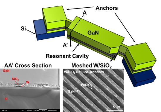
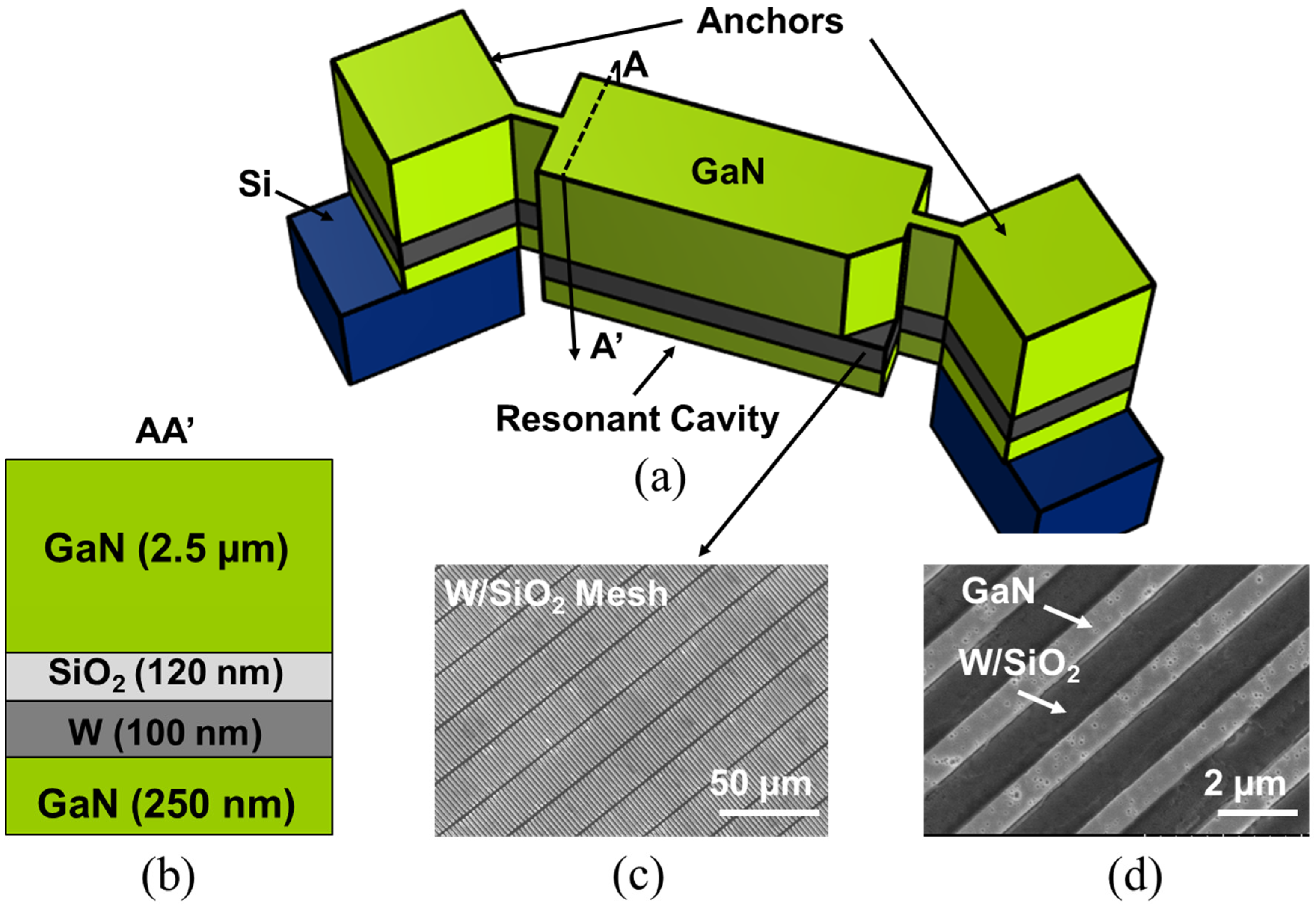
2. Resonator Architecture

2.1. Regrowth of GaN on Embedded Metal Grids

In order to eliminate the need for backside processing of the wafer for releasing the resonant structure, resonant devices need to be released from the frontside. This requires a bottom electrode, embedded in the resonant structure during growth. However, as mentioned before, GaN cannot be directly grown on solid metal layers and the epitaxial growth has to start from a material with similar crystalline orientation. Using a meshed metal electrode on a GaN seed layer, the nucleation can still start from the bottom GaN layer, while a grid of metal is embedded in the resonant structure. The choice of metal is critical since it has to endure a high growth temperature (~1100 °C) and should not diffuse into the top GaN layers. For this purpose, tungsten (W) is used as the metal layer and is capped with a thin silicon dioxide (SiO2) layer to prevent its diffusion into the GaN device layer.
The fabrication process starts with the growth of the buffer layer on a Si (111) substrate. In this work, we used a commercial 500 nm-thick unintentionally-doped (UID) GaN template grown on a Si (111) substrate purchased from Kyma Technologies [12]. Next, the GaN buffer layer was patterned and etched with 250 nm-deep trenches using a chlorine (Cl2) based plasma recipe (Figure 2a) and refilled with sputter-deposited W and evaporated SiO2 layers of ~120 nm and ~100 nm-thick, respectively (Figure 2b). The W/SiO2 patterning was done using a lift-off process. The W/SiO2 formed a pattern such that GaN can be partially exposed to serve as the seed layer for the subsequent GaN regrowth. The sample surface was cleaned of organic contaminants with oxygen (O2) plasma, acetone, and Isopropyl alcohol (IPA). Hydrogen peroxide (H2O2) wet surface cleaning was then performed to clean any trace of exposed W. Exposed W can diffuse into regrown GaN layer if it is not capped well with SiO2. The sample was returned to the metal-organic chemical vapor deposition (MOCVD) reactor to regrow the thick GaN layer. The regrowth was done at National Chiao Tung University (Taiwan), using a Veeco D75 MOCVD system. The growth temperature was 1070 °C, with a V/III ratio of 1500. Nitrogen (N2) and hydrogen (H2) were used as the environment gases with H2 as the carrier gas. The growth rate was ~2.8 μm/h. The thickness of the regrown GaN is measured to be ~2.5 μm (Figure 3).
Figure 2. SEM images showing (a) 250-nm deep trenches made in GaN, forming a grid-like pattern; (b) trenches are refilled with W/SiO2. The darker regions are the W/SiO2 trenches, connected all through the sample, with GaN islands exposed to act as the seed layer for the GaN regrowth initiation. It is important for the GaN islands to have a fairly similar height as the W/SiO2 trenches to ensure smooth regrown GaN surface.
Materials 08 01204 g002
Figure 3. SEM Images of the cross-section of the regrown GaN, (a) on a reference GaN buffer layer of 500 nm thickness with no pattterns. The total thickness of the GaN stack is ~3 μm. (b) GaN regrown on W/SiO2 structures and GaN islands. The regrowth of GaN has well-coalesced and a uniform film is grown on top of the meshed metal electrode. W and SiO2 layers are marked.
Materials 08 01204 g003

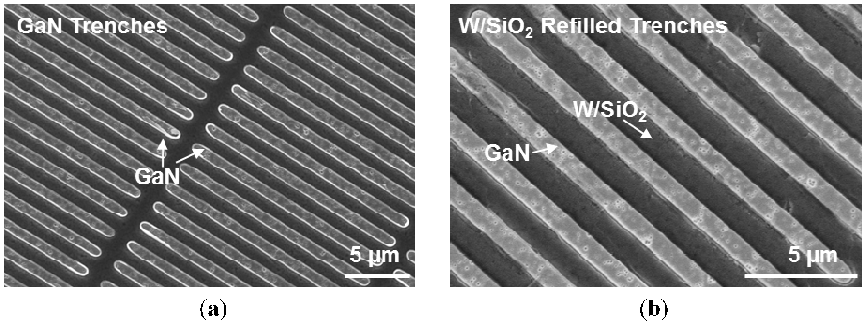
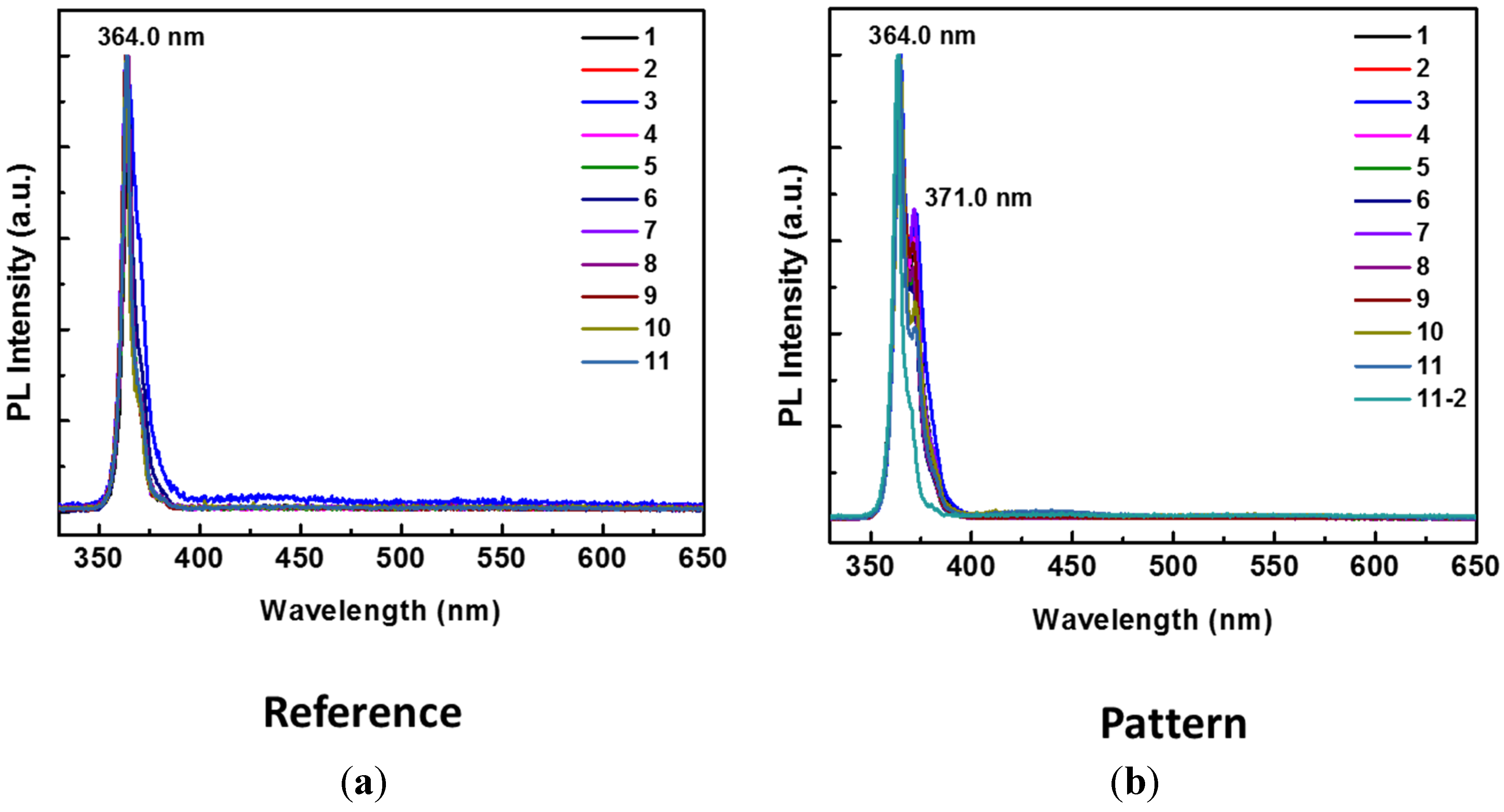
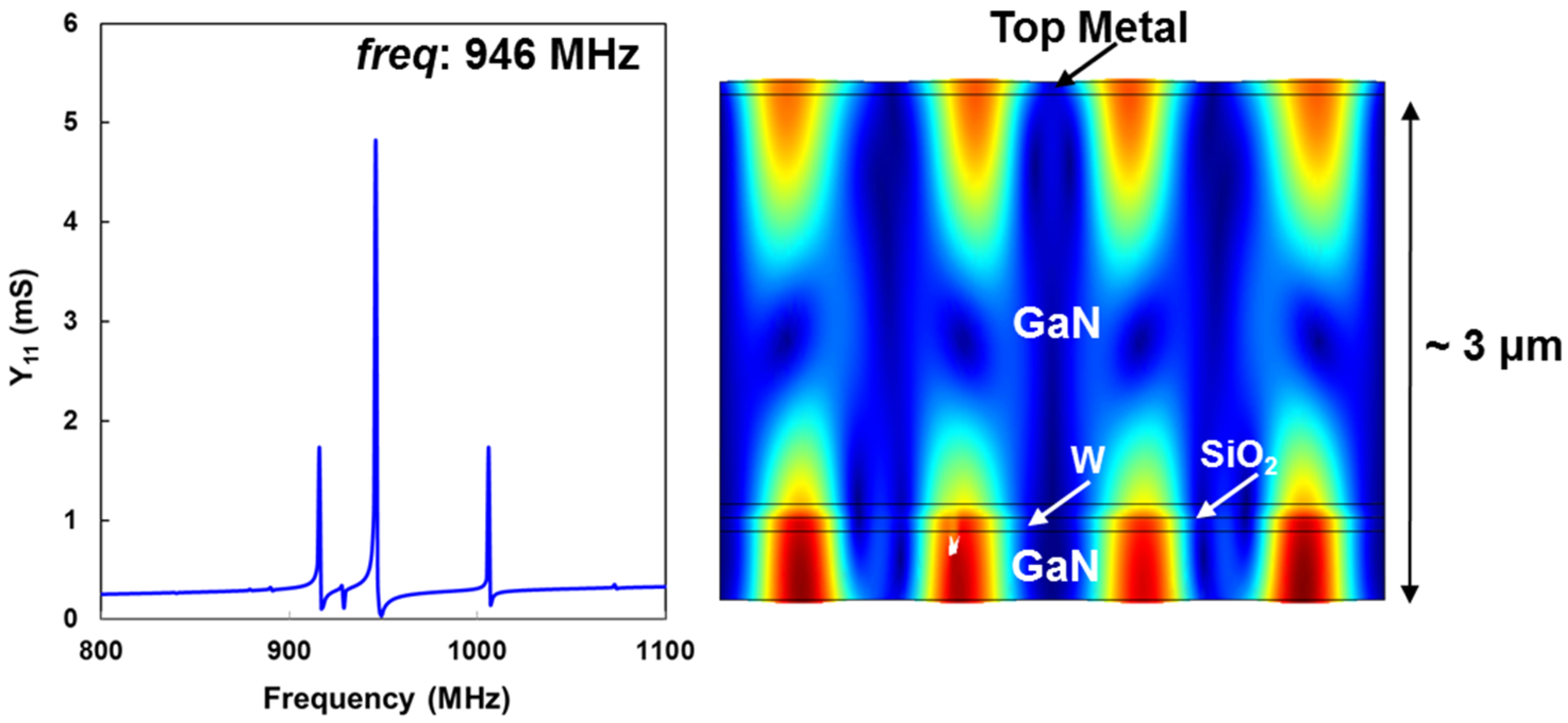
2.2. Experimental Results

The regrown GaN on the patterned seed layer is characterized and compared against GaN regrown on non-patterned GaN seed layer (reference). Photoluminescence (PL) measurements are taken to prove that the quality of GaN formed on the patterned structure is not degraded. Results shown in Figure 4 demonstrate that high-quality GaN layers can be grown on a patterned metal electrode. The ability to grow GaN on embedded metal electrodes opens up many exciting fields using Metal-GaN-Metal structures.
Figure 4. Room temperature photoluminescence (PL) measurement of 11 different points on (a) the reference sample, where GaN is grown on a thin GaN buffer layer without any patterns and embedded metals, or the reference, and (b) on the W/SiO2 patterned structures. The PL measurements clearly indicate the GaN peak (at 364 nm) is not degraded in (b).
Materials 08 01204 g004

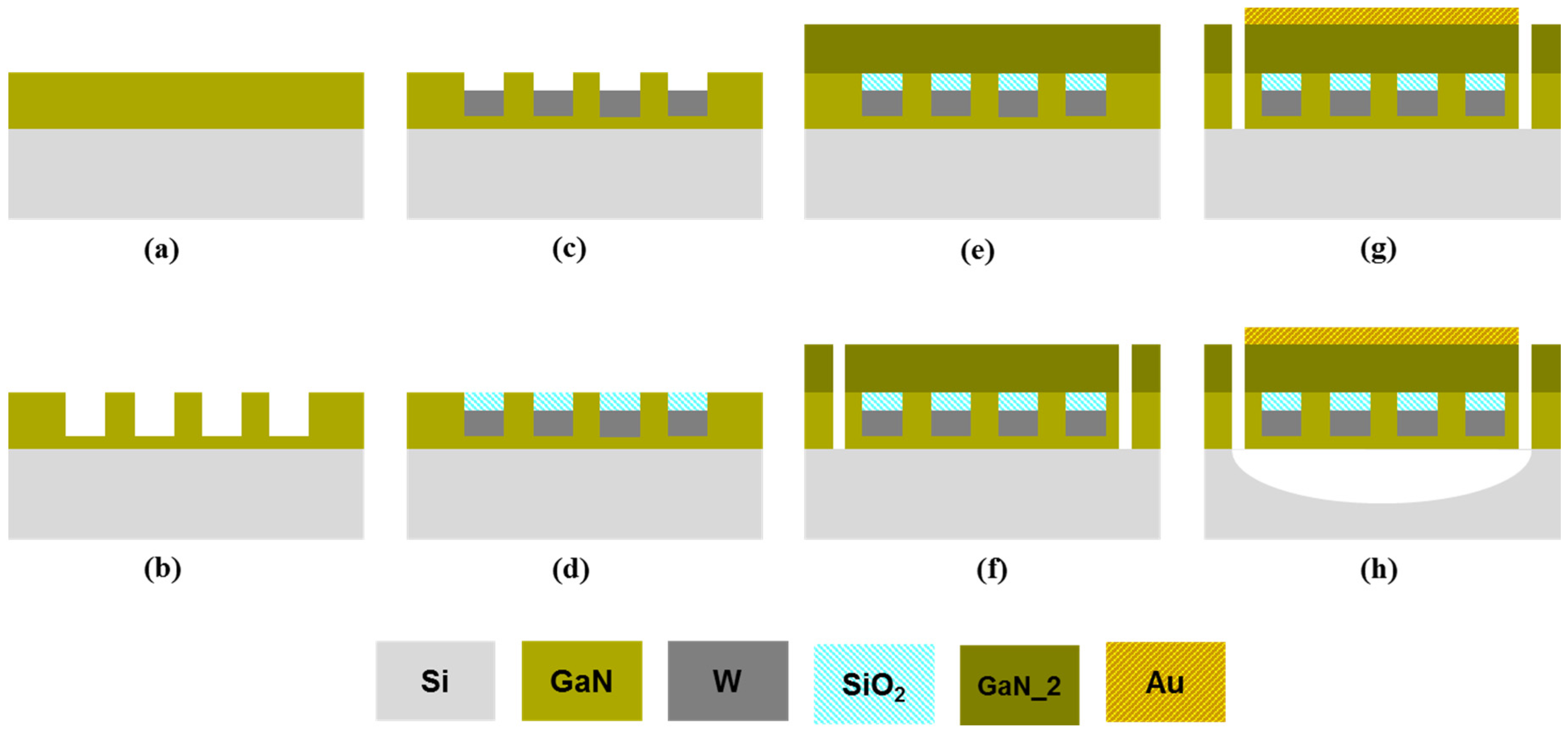
3. Resonator Fabrication Overview

As discussed in the earlier sections, one of the biggest challenges in the fabrication of GaN bulk acoustic resonators is the ability to epitaxially grow GaN on metal electrodes. Using the method shown in Section 2 and the stack shown in Figure 3, by depositing a top metal electrode on the regrown GaN and subsequently releasing the devices from the frontside using XeF2, GaN BAW resonators can be realized. An exemplary schematic of the proposed GaN resonator is shown in Figure 5a and the fabrication steps are discussed in detail in Figure 6. After realization of the stack shown in Figure 3, the thick GaN layer is patterned to form the contours of the resonator. Access to the Si substrate is realized through vias etched in GaN for the release step. The top electrode is then deposited on top of the GaN layer. The devices are finally released from the frontside using XeF2 that removes the Si substrate isotropically. Alternatively, cavity wafers (wafers with a cavity under the Si device layer) can be used instead of frontside isotropic release to fabricate free-standing devices.

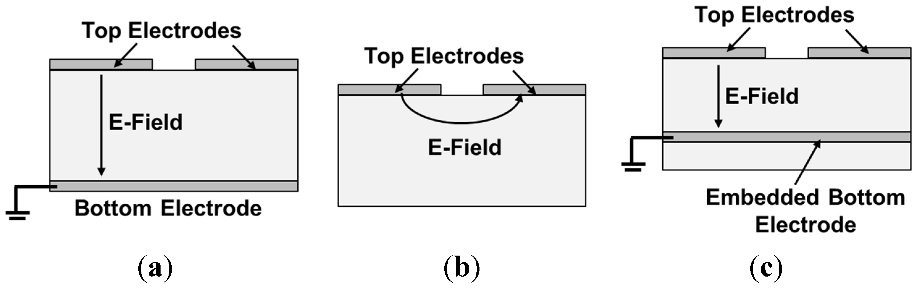
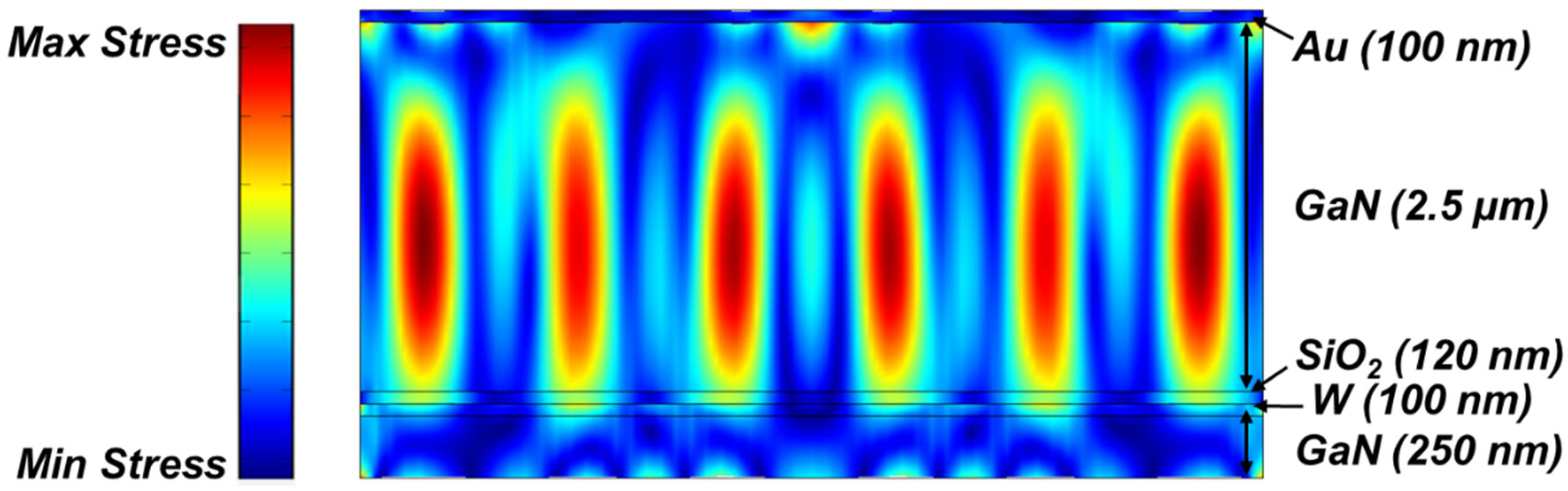
4. Placement of the W/SiO2 Meshed Bottom Electrode

One of the biggest advantages of our approach is the ability to optimize the bottom electrode location within the resonator stack. The placement of the bottom electrode affects several parameters in the resonator performance, such as Q, Kt2, and temperature coefficient of frequency (TCF). Figure 7 shows the simulated admittance response of the resonator with the stack shown in Figure 5b. The admittance of the resonator is plotted around the thickness-mode resonance frequency along with the displacement profile of the same thickness-extensional mode.
Figure 5. (a) An exemplary schematic of a GaN resonator with a thick GaN layer grown on W/SiO2 embedded electrodes. (b) The resonant stack schematic with a total thickness of ~3 μm. (c,d) SEM images of the GaN trenches before the GaN regrowth.
Materials 08 01204 g005
Figure 6. Fabrication steps of GaN resonator with embedded bottom electrode. (a) A thin layer of GaN is grown on a Si (111) substrate, (b) 250 nm deep trenches are made in the GaN layer using BCl3/Cl2 plasma etch, (c) the trenches are filled with sputtered W and (d) evaporated SiO2, (e) GaN device layer is regrown on the W/SiO2 mesh, starting from the bottom GaN seed layer, (f) trenches are made through the GaN layer to access the Si substrate, (g) the top metal is deposited on the device area, (h) the resonator is released with XeF2 isotropic etch.
Materials 08 01204 g006
Another advantage of using embedded electrode with the SiO2 diffusion barrier is that the SiO2 can also act as a passive temperature compensation layer. Passive compensation is realized by using materials with opposite temperature coefficient of elasticity (TCE). Most materials (e.g., Si, AlN, GaN) have a negative TCE, and therefore their resonance frequency decreases with an increase in temperature. SiO2, unlike GaN, has a positive TCE (TCE of SiO2: ~+160 ppm/K, TCE of GaN: ~−60 ppm/K) and can be used to cancel the temperature-induced frequency drift in GaN resonators [13]. Both the volume and location of SiO2 structures play a critical role in determining the TCF of a resonator. It is shown in [14] that placing embedded SiO2 structures at the location of maximum stress is most effective in reducing TCF values. In [13], we have shown GaN micromechanical resonators with a 400 nm thick blanket SiO2 on the top surface to reduce the value of TCF to ~−15 of ppm/K. Using the structure in this work, even with a thinner SiO2 layer, which is placed at high stress locations, significantly higher levels of temperature compensation can be achieved (Figure 8). More specifically, the first-order TCF of the GaN resonator with our proposed architecture can be canceled out for the fundamental thickness-mode resonance (Figure 8).
Figure 7. COMSOL [15] simulation of |Y11| response of a GaN bulk acoustic wave (BAW) resonator along with displacement profile of the thickness-mode resonance at 946 MHz.
Materials 08 01204 g007
Figure 8. COMSOL simulation of the stress profile of the fundamental thickness-mode resonance at 946 MHz for the stack in Figure 5b. 120 nm thick embedded oxide layer is placed within the stack, fully compensating the temperature-induced frequency shifts of the fundamental thickness-mode resonance of the GaN piezoelectric resonator. Assuming a TCE value of -60 ppm/K for GaN, and TCE of +160 ppm/K for SiO2 [13], TCF of the resonator is simulated to be ~−5 ppm/K for the stack shown above.
Materials 08 01204 g008

5. Conclusions

This work demonstrated a novel structure for GaN bulk acoustic resonators using vertical electric field for efficient piezoelectric actuation. In this approach, DRIE and backside metal sputtering is not used in the fabrication process as a bottom metal electrode is embedded in the GaN stack during the growth process and the GaN structural layer is released from the frontside with XeF2 etching of Si substrate. Using this approach, the placement of the bottom electrode can be optimized to maximize the charge pickup and displacement at resonance. Furthermore the embedded silicon dioxide protective layer used to prevent diffusion of tungsten in the regrown GaN layer can also be used for temperature compensation.

Acknowledgments

The authors would like to acknowledge the staff of the Lurie Nanofabrication Facility at the University of Michigan and Dr. Hsun-Chih Kuo for their assistance with fabrication. This work was supported by the National Science Foundation under award NO. 1002036 and NO. 1055308.

Author Contributions

A.A. designed and fabricated the grid embedded metals. M.R. and A.A. contributed to the theoretical models and analysis and wrote the manuscript with input from P.-C.K., C.-Y.L., C.-C.L. performed the GaN regrowth and the PL measurements with input from H.-C.K. Both M.R. and P.-C.K. directed the project.

Conflicts of Interest

The authors declare no conflict of interest.

References

  1. Gokhale, V.J.; Roberts, J.; Rais-Zadeh, M. High performance bulk mode gallium nitride resonators and filters. In Proceedings of the International Conference on Solid-State Sensors, Actuators and Microsystems (Transducers), Beijing, China, 5–9 June 2011; pp. 926–929.
  2. Ansari, A.; Gokhale, V.; Roberts, J.; Rais-Zadeh, M. Monolithic integration of GaN-based micromechanical resonators and HEMTs for timing application. In Proceedings of the 2012 IEEE International Electron Device Meeting, San Francisco, CA, USA, 10–13 December 2012.
  3. Ansari, A.; Rais-Zadeh, M. An 8.7 GHz GaN micromechanical resonator with an integrated AlGaN/GaN HEMT. In Proceedings of the Solid-State Sensors, Actuators and Microsystems Workshop (Hilton Head Workshop), Hilton Head, CA, USA, 8–12 June 2014; pp. 295–296.
  4. Ansari, A.; Gokhale, V.J.; Thakar, V.A.; Roberts, J.; Rais-Zadeh, M. Gallium nitride-on-silicon micromechanical overtone resonators and filters. In Proceedings of the IEEE International Electron Device Meeting, Washington, DC, USA, 5–7 December 2011; pp. 485–488.
  5. Niebelschutz, F.; Cimalla, V.; Tonisch, K.; Haupt, C.; Brückner, K.; Stephan, R.; Hein, M.; Ambacher, O. AlGaN/GaN-based MEMS with two-dimensional electron gas for novel sensor applications. Phys. Status Solidi 2008, 5, 1914–1916. [Google Scholar] [CrossRef]
  6. Faucher, M.; Cordier, Y.; Werquin, M.; Buchaillot, L.; Gaquiere, C.; Theron, D. Electromechanical transconductance properties of a GaN MEMS resonator with fully integrated HEMT transducers. J. Microelectromech. Syst. 2012, 21, 370–378. [Google Scholar]
  7. Ansari, A.; Rais-Zadeh, M. HEMT-Based readout of a thickness-mode AlGaN/GaN resonator. In Proceedings of the IEEE Electron Device Meeting, Washington, DC, USA, 9–11 December 2013; pp. 1–4.
  8. Popa, L.C.; Weinstein, D. Switchable piezoelectric transduction in AlGaN/GaN MEMS resonators. In Proceedings of the 17th International Conference on Solid-State Sensors, Actuators and Microsystems (Transducers), Barcelona, Spanish, 16–20 June 2013; pp. 16–20.
  9. Ansari, A.; Rais-Zadeh, M. A thickness-mode AlGaN/GaN resonant body high electron mobility transistor. IEEE Trans. Electron Devices 2014, 61, 1006–1013. [Google Scholar] [CrossRef]
  10. Popa, L.C.; Weinstein, D. L-Band lamb mode resonators in gallium nitride MMIC technology. In Proceedings of the International Frequency Control Symposium, Taibei, Taiwan, 19–22 May 2014; pp. 559–562.
  11. Popa, L.C.; Weinstein, D. 2DEG electrodes for piezoelectric transduction of AlGaN/GaN MEMS resonators. In Proceedings of the European Frequency and Time Forum & International Frequency Control Symposium (EFTF/IFC), Prague, Czech Republic, 21–25 July 2013; pp. 922–925.
  12. Kyma Techologies. Available online: http://www.kymatech.com/ (accessed on 12 March 2015).
  13. Ansari, A.; Rais-Zadeh, M. A temperature-compensated gallium nitride micromechanical resonator. IEEE Electron Device Lett. 2014, 35, 1127–1129. [Google Scholar] [CrossRef]
  14. Thakar, V.A.; Wu, Z.; Peczalski, A.; Rais-Zadeh, M. Piezoelectrically transduced temperature-compensated flexural-mode silicon resonators. IEEE J. Microelectromech. Syst. 2013, 22, 819–823. [Google Scholar] [CrossRef]
  15. COMSOL. Available online: http://www.comsol.com/ (accessed on 14 March 2015).

