Single Layer Broadband Anti-Reflective Coatings for Plastic Substrates Produced by Full Wafer and Roll-to-Roll Step-and-Flash Nano-Imprint Lithography

Abstract
:1. Introduction
2. Results and Discussion
2.1. ARCs Produced by Full Wafer Step-and-Flash NIL
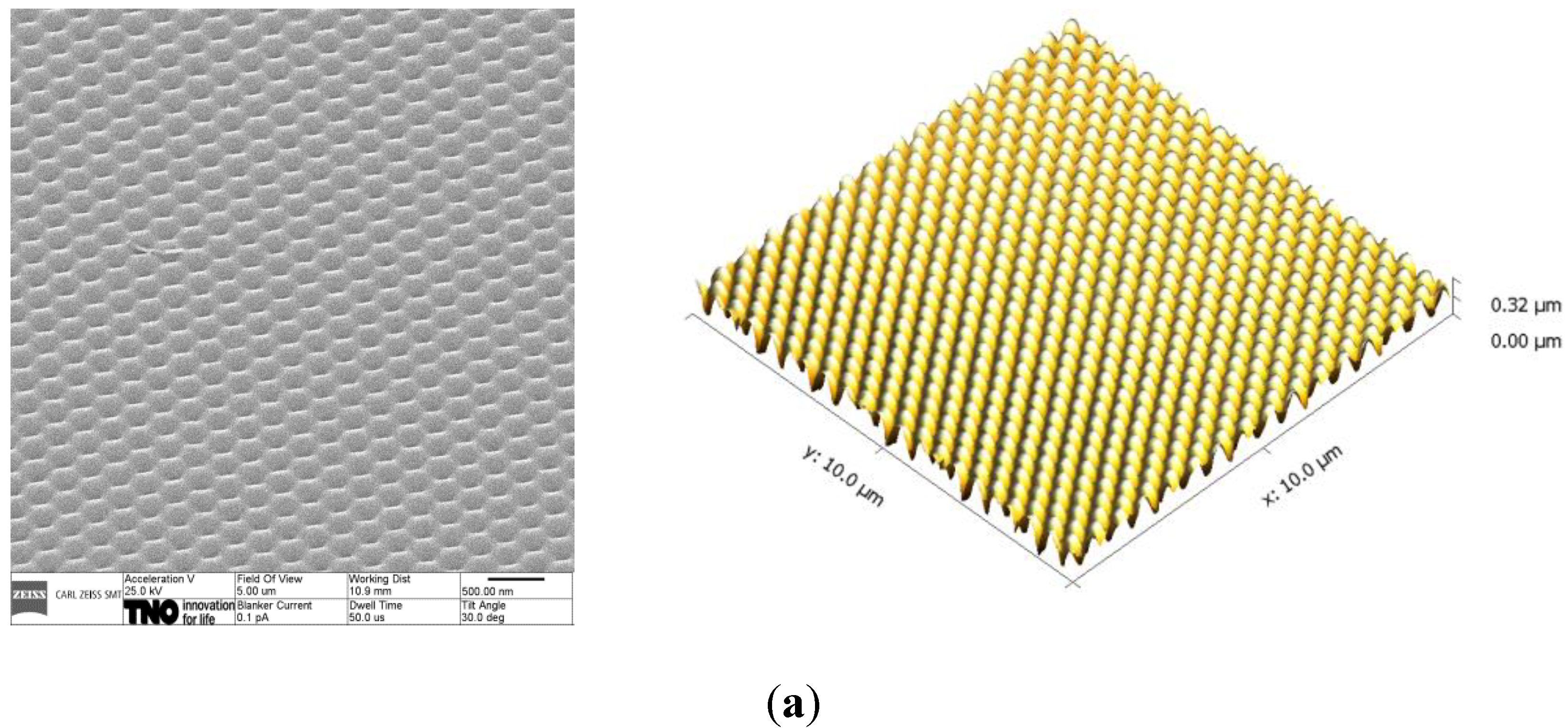
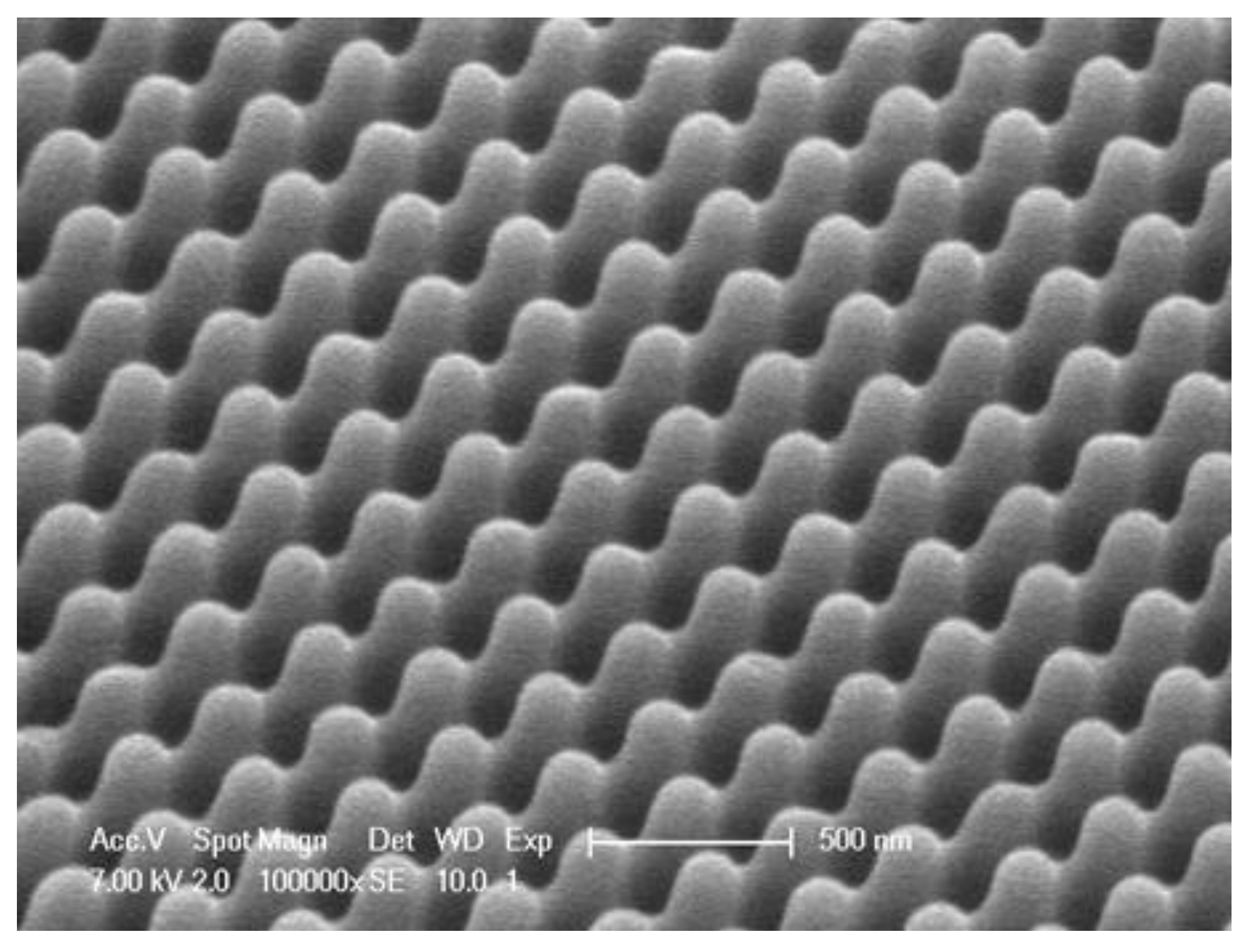
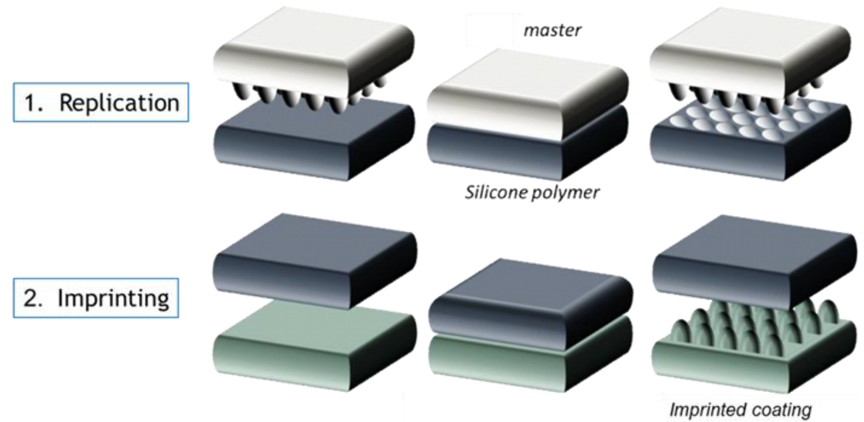
2.1.1. Replication and Imprint Process


| Material | Lateral pitch (nm) | Average depth (nm) |
|---|---|---|
| Holotools mold | 250 | 300 |
| h-PDMS | 250 | 300 |
| Ormocomp | 250 | 284 |
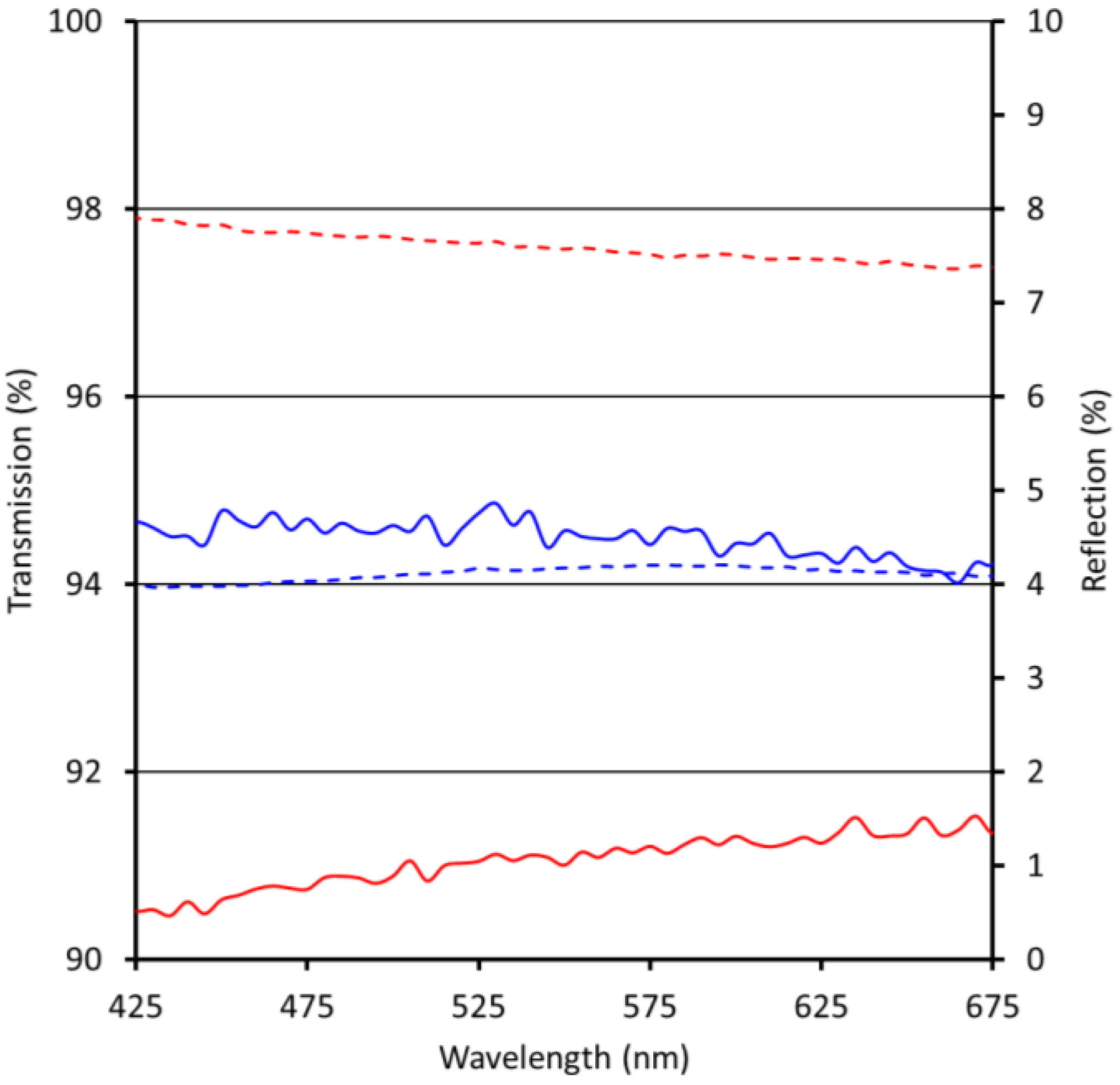
2.1.2. Optical Properties of Moth Eye-Structured Ormocomp Coating


2.1.3. Adhesion and Scratch Resistance
| Coating | Imprint | Undamaged-damaged pencil hardness |
|---|---|---|
| Ormocomp | moth eye-structured | <4B |
| Ormocomp | non-structured | HB–F |
| Uncoated polycarbonate | 2B–B | |
| Coating | Imprint | Undamaged-damaged pencil hardness |
|---|---|---|
| Ormocomp | moth eye-structured | <4B |
| Ormocomp | non-structured | 2H–3H |
| Uncoated PMMA | 3H–4H | |
2.1.4. Durability of the ARCs
| Uncoated/coated PMMA | ΔR [%] Damp heat 1000 h 85 °C 85% RH | ΔR [%] Thermal cycling 200 cycles −40/85 °C | ΔR [%] Humidity freeze 10 cycles 85 °C 85% RH to −40 °C |
|---|---|---|---|
| Uncoated PMMA | +0.10 | 0.00 | +0.07 |
| Ormocomp non-structured | +1.11 | +0.93 | +0.57 |
| Ormocomp moth eye-structured | +1.16 | −0.08 | −0.32 |
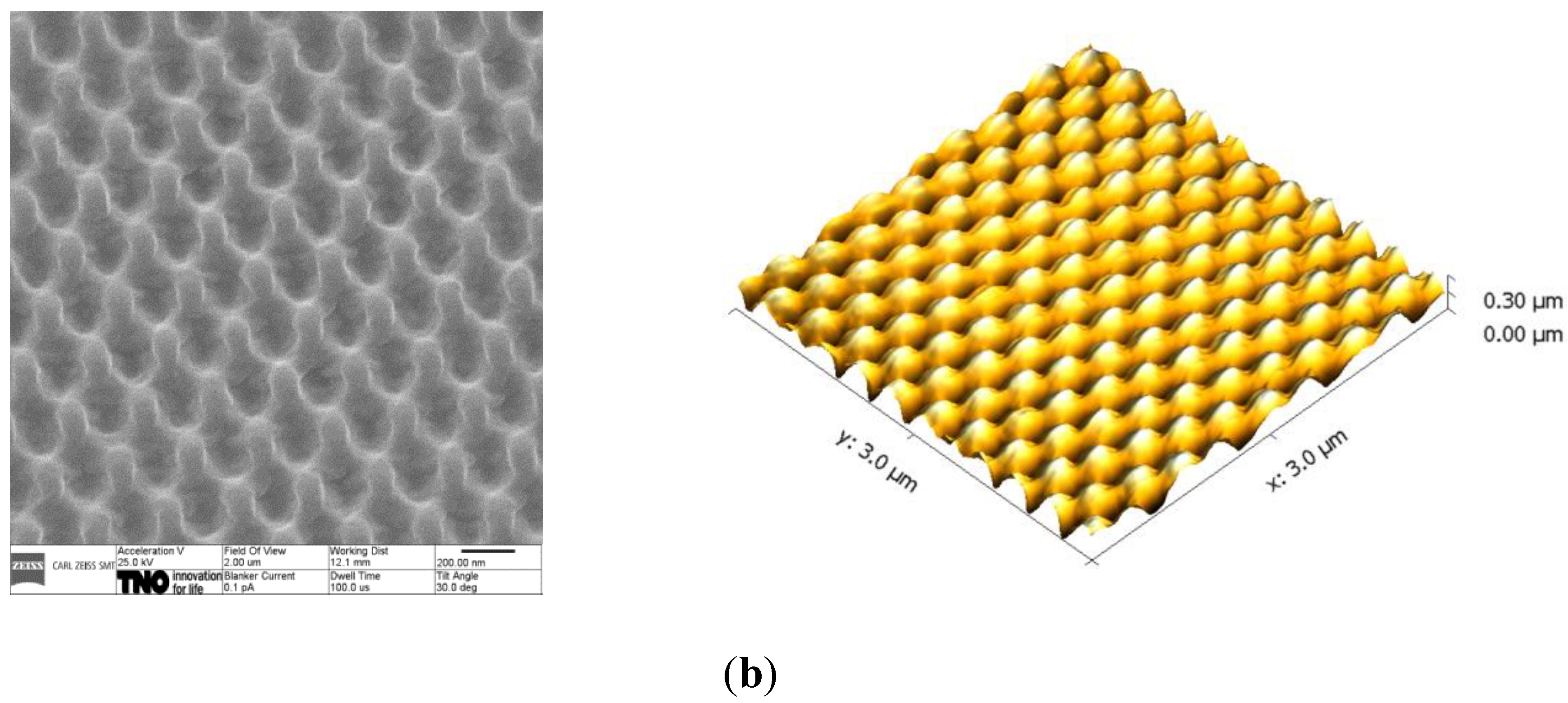
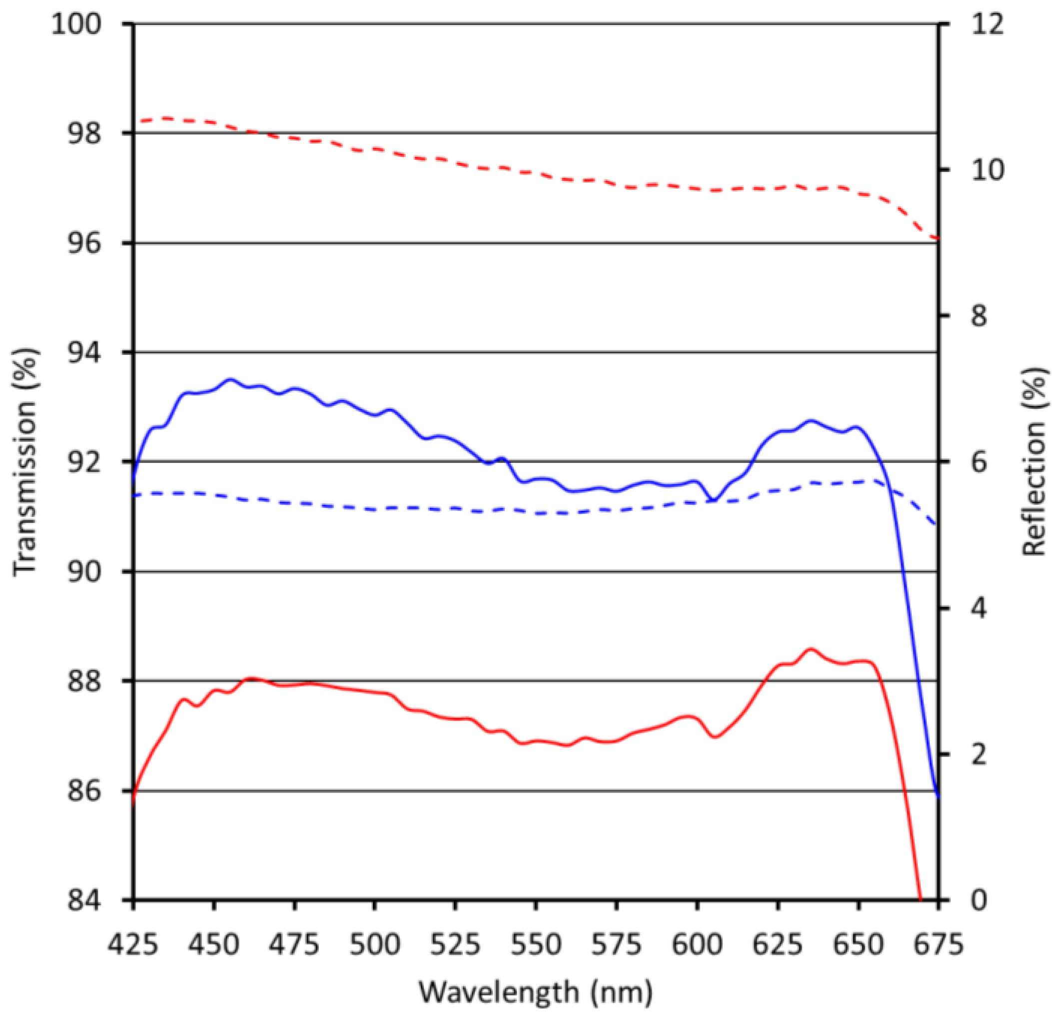
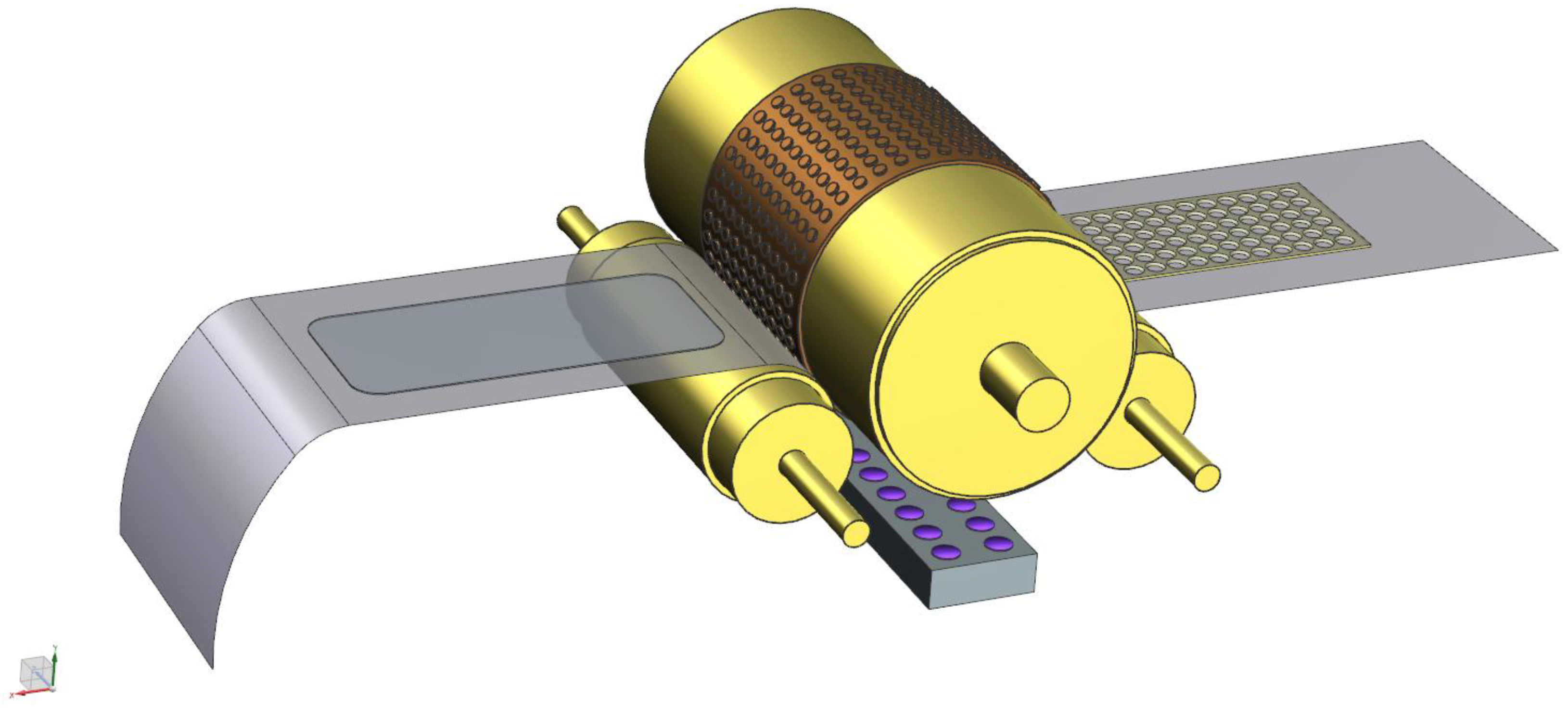
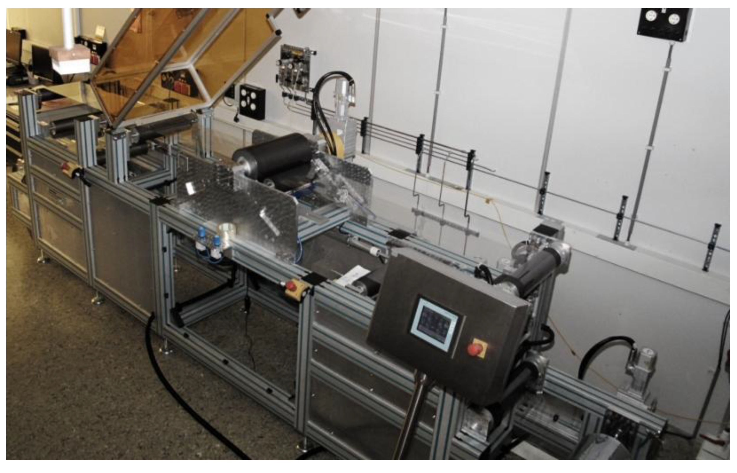
2.2. Anti-Reflective Coatings Produced by Roll-to-Roll UV NIL


3. Experimental Section
3.1. Materials and Equipment
3.2. The Wafer-by-Wafer NIL Process

3.2.1. Preparation of the Replica
3.2.2. Structuring of the Ormocomp Resist
3.3. Characterization of Nanostructured Surfaces
3.3.1. HIM
3.3.2. AFM
3.4. Optical Characterization
3.5. Scratch Resistance Measurements
3.6. Durability Tests
4. Conclusions
Acknowledgments
Conflicts of Interest
References
- MacLeod, H.A.; MacLeod, A. Thin-Film Optical Filters; CRC Press: Bristol, UK, 2001. [Google Scholar]
- Chen, D. Anti-reflection (AR) coatings made by sol-gel processes: A review. Sol. Energy Mater. Sol. Cells 2001, 68, 313–336. [Google Scholar] [CrossRef]
- Ibn-Elhaj, M.; Schadt, M. Optical polymer thin films with isotropic and anisotropic nano-corrugated surface topologies. Nature 2001, 410, 796–799. [Google Scholar] [CrossRef] [PubMed]
- Chen, D.; Yan, Y.; Westenberg, E.; Niebauer, D.; Sakaitani, N.; Chaudhuri, S.R.; Sato, Y.; Takamatsu, M. Development of anti-reflection (AR) coating on plastic panels for display applications. J. Sol-Gel Sci. Technol. 2000, 19, 77–82. [Google Scholar] [CrossRef]
- Schottner, G.; Rose, K.; Posset, U. Scratch and abrasion resistant coatings on plastic lenses—State of the art, current developments and perspectives. J. Sol-Gel Sci. Technol. 2003, 27, 71–79. [Google Scholar] [CrossRef]
- Gombert, A.; Glaubitt, W.; Rose, K.; Dreibholz, J.; Bläsi, B.; Heinzel, A.; Sporn, D.; Döll, W.; Wittwer, V. Anti-reflective transparent covers for solar devices. Sol. Energy 2000, 68, 357–360. [Google Scholar] [CrossRef]
- Gombert, A.; Glaubitt, W.; Rose, K.; Dreibholz, J.; Bläsi, B.; Heinzel, A.; Sporn, D.; Döll, W.; Wittwer, V. Subwavelength-structured antireflective surfaces on glass. Thin Solid Films 1999, 351, 73–78. [Google Scholar] [CrossRef]
- Chen, J.J.; Sun, K.W. Enhancement of the light conversion efficiency of silicon solar cells by using nanoimprint anti-reflection layer. Sol. Energy Mater. Sol. Cells 2010, 94, 629–633. [Google Scholar] [CrossRef]
- Forberich, K.; Dennler, G.; Scharber, M.C.; Hingert, K.; Fromherz, T.; Brabec, C.J. Performance improvement of organic solar cells with moth eye anti-reflection coating. Thin Solid Films 2008, 516, 7167–7170. [Google Scholar] [CrossRef]
- Wu, D.; Zhao, Y.B.; Wu, S.Z.; Liu, Y.F.; Zheng, H.; Zhao, S.; Feng, J.; Chen, Q.D.; Ma, D.G.; Sun, H.B. Simultaneous efficiency enhancement and self-cleaning effect of white organic light-emitting devices by flexible antireflection films. Opt. Lett. 2011, 36, 2635–2637. [Google Scholar] [CrossRef] [PubMed]
- Jeong, S.H.; Kim, J.K.; Kim, B.S.; Shim, S.H.; Lee, B.T. Characterization of SiO2 and TiO2 films prepared using rf magnetron sputtering and their application to anti-reflection coating. Vacuum 2004, 76, 507–515. [Google Scholar] [CrossRef]
- Kim, J.Y.; Han, Y.K.; Kim, E.R.; Suh, K.S. Two-layer hybrid anti-reflection film prepared on plastic substrates. Curr. Appl. Phys. 2002, 2, 123–127. [Google Scholar] [CrossRef]
- Glaubitt, W.; Löbmann, P. Antireflective coatings prepared by sol-gel processing: Principles and applications. J. Eur. Ceram. Soc. 2012, 32, 2995–2999. [Google Scholar] [CrossRef]
- Pénard, L.; Gacoin, T.; Boilot, J.P. Functionalized sol-gel coatings for optical applications. Acc. Chem. Res. 2007, 40, 895–902. [Google Scholar] [CrossRef] [PubMed]
- Hiller, J.; Mendelsohn, J.D.; Rubner, M.F. Reversibly erasable nanoporous anti-reflective coatings from polyelectrolyte multilayers. Nat. Mater. 2002, 1, 59–63. [Google Scholar] [CrossRef] [PubMed]
- Du, Y.; Luna, L.E.; Tan, W.S.; Rubner, M.F.; Cohen, R.E. Hollow silica nanoparticles in UV—Visible antireflection coatings for poly(methyl methacrylate) substrates. ACS Nano 2010, 4, 4308–4316. [Google Scholar] [CrossRef] [PubMed]
- Guillemot, F.; Brunet-Bruneau, A.; Bourgeat-Lami, E.; Gacoin, T.; Barthel, E.; Boilot, J.P. Latex-templated silica films: Tailoring porosity to get a stable low-refractive index. Chem. Mater. 2010, 22, 2822–2828. [Google Scholar] [CrossRef]
- Huang, Y.F.; Chattopadhyay, S.; Jen, Y.J.; Peng, C.Y.; Liu, T.A.; Hsu, Y.K.; Pau, C.L.; Lo, H.C.; Hsu, C.H.; Chang, Y.H.; et al. Improved broadband and quasi-omnidirectional anti-reflection properties with biomimetic silicon nanostructures. Nat. Nanotechnol. 2007, 2, 770–774. [Google Scholar] [CrossRef] [PubMed]
- Clapham, P.B.; Hutley, M.C. Reduction of lens reflexion by the ‘moth eye’ principle. Nature 1973, 244, 281–282. [Google Scholar] [CrossRef]
- Kikuta, H.; Toyota, H.; Yu, W. Optical elements with subwavelength structured surfaces. Opt. Rev. 2003, 10, 63–73. [Google Scholar] [CrossRef]
- Boden, S.A.; Bagnall, D.H. Tunable reflection minima of nanostructured antireflective surfaces. Appl. Phys. Lett. 2008, 93, 133108:1–133108:3. [Google Scholar] [CrossRef]
- Ai, D.; Lu, W.; Xu, H.; Yang, B.; Huang, C.; Xu, M.; Gao, L.; Weng, Z.; Chi, L. Simple approach to wafer-scale self-cleaning anti-reflective silicon surfaces. Langmuir 2009, 25, 7769–7772. [Google Scholar] [CrossRef] [PubMed]
- Ting, C.J.; Huang, M.C.; Tsai, H.Y.; Chou, C.P.; Fu, E.C. Low cost fabrication of large-area anti-reflection films from polymer by nanoimprint/hot embossing technology. Nanotechnology 2008, 19, 205501:1–205501:20. [Google Scholar] [CrossRef]
- Chou, S.Y.; Krauss, P.R.; Renstrom, P.J. Imprint of sub-25 nm vias and trenches in polymers. Appl. Phys. Lett. 1995, 67, 3114–3116. [Google Scholar] [CrossRef]
- Chou, S.Y.; Krauss, P.R.; Renstrom, P.J. Imprint lithography with 25 nm resolution. Science 1996, 272, 85–87. [Google Scholar] [CrossRef]
- Chou, S.Y.; Krauss, P.R.; Renstrom, P.J. Nanoimprint lithography. J. Vac. Sci. Technol. B Electron. Nanom. Struct. 1996, 14, 4129–4133. [Google Scholar] [CrossRef]
- Gates, B.D.; Xu, Q.; Stewart, M.; Ryan, D.; Willson, C.G.; Whitesides, G.H. New approaches to nanofabrication: Molding, printing and other techniques. Chem. Rev. 2005, 105, 1171–1196. [Google Scholar] [CrossRef] [PubMed]
- Chou, S.Y.; Krauss, P.R.; Zhang, W.; Guo, L.; Zhuang, L. Sub-10 nm imprint lithography and applications. J. Vac. Sci. Technol. B Electron. Nanom. Struct. 1997, 15, 2897–2904. [Google Scholar] [CrossRef]
- Guo, L.J.; Phys, J. Recent progress in nanoimprint technology and its applications. J. Phys. D Appl. Phys. 2004, 37, R123:1–R123:11. [Google Scholar] [CrossRef]
- Collburn, M.; Johnson, S.C.; Stewart, M.D.; Damle, S.; Bailey, T.C.; Choi, B.; Wedlake, M.; Michaelson, T.B.; Sreenivasan, S.V.; Ekerdt, J.G.; et al. Step and flash nanoimprint lithography: A new approach to high-resolution patterning. Proc. SPIE 1999, 3676, 379–389. [Google Scholar]
- Bailey, T.; Choi, B.J.; Colburn, M.; Heissel, M.; Shaya, S.; Ekerdt, J.G.; Sreenivasan, S.V.; Willson, C.G. Step and flash imprint lithography: Template surface treatment and defect analysis. J. Vac. Sci. Technol. B Electron. Nanom. Struct. 2000, 18, 3572–3577. [Google Scholar] [CrossRef]
- Menard, E.; Meitl, M.A.; Sun, Y.; Park, J.U.; Shir, D.J.L.; Nam, Y.S.; Jeon, S.; Rogers, J.A. Micro- and nanopatterning techniques for organic electronic and opto-electronic systems. Chem. Rev. 2007, 107, 1117–1160. [Google Scholar] [CrossRef] [PubMed]
- Khang, D.Y.; Yoon, H.; Lee, H.H. Room-temperature imprint lithography. Adv. Mater. 2001, 13, 749–752. [Google Scholar] [CrossRef]
- Chen, Y.; Ohlberg, D.A.A.; Li, X.; Stewart, D.R.; Williams, R.S.; Jeppesen, J.O.; Wielsen, K.A.; Stocklart, J.F.; Olynick, D.L.; Andersen, E. Nanoscale molecular-switch devices fabricated by imprint lithography. Appl. Phys. Lett. 2003, 82, 1610–1612. [Google Scholar] [CrossRef]
- Hoff, J.D.; Cheng, L.J.; Meyhofer, E.; Guo, L.J.; Hunt, A.J. Nanoscale protein patterning by imprint lithography. Nano Lett. 2004, 4, 853–857. [Google Scholar] [CrossRef]
- Ahn, S.W.; Lee, K.D.; Kim, J.S.; Kim, S.H.; Park, J.D.; Lee, S.H.; Yoon, P.W. Fabrication of a 50 nm half-pitch wire grid polarizer using nanoimprint lithography. Nanotechnology 2005, 16, 1874:1–1874:9. [Google Scholar] [CrossRef]
- Guo, L.; Krauss, P.R.; Chon, S.J. Nanoscale silicon field effect transistors fabricated using imprint lithography. Appl. Phys. Lett. 1997, 71, 1881–1883. [Google Scholar] [CrossRef]
- Austin, M.D.; Zhang, W.; Ge, H.; Wassermann, D.; Lyon, S.A.; Chou, S.Y. 6 nm half-pitch lines and 0.04 μm2 static random access memory patterns by nanoimprint lithography. Nanotechnology 2005, 16, 1058:1–1058:8. [Google Scholar] [CrossRef]
- Truskett, V.N.; Watts, M.P.G. Trends in imprint lithography for biological applications. Trends Biotechnol. 2006, 24, 312–317. [Google Scholar] [CrossRef] [PubMed]
- Pozzato, A.; Zilio, S.D.; Fois, G.; Vendramin, D.; Misturo, G.; Belotti, M.; Chen, Y.; Natali, M. Superhydrophobic surfaces fabricated by nano-imprint lithography. Microelectron. Eng. 2006, 83, 884–888. [Google Scholar] [CrossRef]
- Rosnick, D.J.; Dauksher, W.J.; Mancini, D.; Nordquist, K.J.; Bailey, T.C.; Johnsson, S.; Stacey, N.; Ekerdt, J.G.; Willson, C.G.; Sreenivasa, S.V.; et al. Imprint lithography for integrated circuit fabrication. J. Vac. Sci. Technol. B Electron. Nanom. Struct. 2003, 21, 2624–2631. [Google Scholar] [CrossRef]
- Malyarchuk, V.; Hua, F.; Merck, N.; Velasquez, V.; White, J.; Nuzzo, R.; Rogers, J. High performance plasmonic crystal sensor formed by soft nanoimprint lithography. Opt. Express 2005, 13, 5669–5675. [Google Scholar] [CrossRef] [PubMed]
- Sun, Y.; Forrest, S.R. Organic light emitting devices with enhanced outcoupling via microlenses fabricated by imprint lithography. J. Appl. Phys. 2006, 100, 073106:1–073106:6. [Google Scholar]
- Cho, H.K.; Jang, J.; Choi, J.H.; Choi, J.; Kim, J.; Lee, J.S.; Lee, B.; Choe, Y.H.; Lee, K.D.; Kim, S.H.; et al. Light extraction enhancement from nano-imprinted photonic crystal GaN-based blue light emitting diodes. Opt. Express 2006, 14, 8654–8660. [Google Scholar] [CrossRef] [PubMed]
- Ferry, V.E.; Verschuuren, M.A.; van Lare, M.C.; Schropp, R.J.; Atwater, H.A.; Polman, A. Optimized spacial correlations for broadband light trapping nanopatterns in high efficiency ultrathin film a-Si: H solar cells. Nano lett. 2011, 11, 4239–4245. [Google Scholar] [CrossRef] [PubMed]
- Battaglia, C.; Hsu, C.M.; Söderström, K.; Escarré, J.; Hang, F.J.; Charrière, M.; Boccard, M.; Despeisse, M.; Alexander, D.T.L.; Cantoni, M.; et al. Light trapping in solar cells: Can periodic beat random? ACS Nano 2012, 6, 2790–2797. [Google Scholar] [CrossRef] [PubMed]
- Söderström, K.; Escarré, J.; Cubero, O.; Hang, F.J.; Perregaux, S.; Ballif, C. UV nano-imprint lithography technique for the replication of back reflectors for n-i-p thin film silicon solar cells. Prog. Photovolt. Res. Appl. 2011, 19, 202–210. [Google Scholar] [CrossRef]
- Jeon, S.; Kong, J.W.; Park, H.D.; Kim, J.J.; Youn, J.R.; Shim, Y.; Jeong, J.H.; Choi, D.G.; Kim, K.D.; Altun, A.O.; et al. Ultraviolet nanoimprinted polymer nanostructure for organic light emitting diode application. Appl. Phys. Lett. 2008, 92, 223307:1–223307:3. [Google Scholar]
- Ji, R.; Hornung, M.; Verschuuren, M.A.; Van de Laar, R.; Van Eekelen, J.; Plachetta, U.; Moeller, M.; Moormann, C. UV enhanced substrate conformal imprint lithography (UV-SCIL) technique for photonic crystal patterning in LED manufacturing. Microelectron. Eng. 2010, 87, 936–967. [Google Scholar]
- Yanagishita, T.; Nishio, K.; Masuda, H. Anti-reflection structures on lenses by nano-imprinting using ordered porous alumina. Appl. Phys. Express 2009, 2, 022001:1–022001:3. [Google Scholar] [CrossRef]
- Chang, T.L.; Cheng, K.Y.; Chou, T.H.; Su, C.C.; Yang, H.P.; Luo, S.W. Hybrid-polymer nanostructures forming an anti-reflection film using two-beam interference and ultraviolet nanoimprint lithography. Microelectron. Eng. 2009, 86, 874–877. [Google Scholar] [CrossRef]
- Chen, Q.; Hubbard, G.; Shields, P.A.; Liu, C.; Allsopp, D.W.E.; Wang, W.N.; Abbott, S. Broadband moth eye antireflection coatings fabricated by low-cost nanoimprinting. Appl. Phys. Lett. 2009, 94, 263118:1–263118:3. [Google Scholar]
- Kim, H.J.; Marcier, A.W.; Garcia, B.; Kwon, D.; Jeffrey, F.; Braymen, S.; Hauschilelt, J.; Taussig, C. Roll-to-roll manufacturing of electronics on flexible substrates using self-aligned imprint lithography (SAIL). J. Soc. Inf. Disp. 2009, 3, 2062–2069. [Google Scholar]
- Stuart, C.; Chen, Y. Roll in and roll out: a path to high-throughput nanoimprint lithography. ACS Nano 2009, 3, 2062–2069. [Google Scholar] [CrossRef] [PubMed]
- Youn, S.W.; Ogiwara, M.; Goto, H.; Takahashi, M.; Maeda, R. Prototype development of a roller imprint system and its application to large area polymer replication for a microstructured optical device. J. Mater. Process. Technol. 2008, 202, 76–85. [Google Scholar] [CrossRef]
- Seo, S.M.; Kim, T.I.; Lee, H.H. Simple fabrication of nanostructure by continuous rigiflex imprinting. Microelectron. Eng. 2007, 84, 567–572. [Google Scholar] [CrossRef]
- Han, J.; Choi, S.; Lee, B.S.; Kang, S. Fabrication of transparent conductive tracks and patterns on flexible substrate using a continuous UV roll imprint lithography. J. Phys. D Appl. Phys. 2009, 42, 115503:1–115503:11. [Google Scholar]
- Jeans, A.; Almanza-Workman, M.; Cobene, R.; Eleter, R.; Garcia, R.; Golmez-Pancorbo, F.; Jackson, W.; Jam, M.; Kim, H.J.; Kwon, O.; et al. Advances in roll-to-roll imprint lithography for display applications. Proc. SPIE 2010, 7637, 763719:1–763719:12. [Google Scholar]
- Moonen, P.F.; Yakimets, I.; Huskens, J. Fabrication of transistors on flexible substrates: from mass printing to high-resolution alternative lithography strategies. Adv. Mater. 2012, 24, 5526–5541. [Google Scholar] [CrossRef] [PubMed]
- Maury, P.; Turkenburg, D.; Stroeks, N.; Giesen, P.; Barbu, I.; Meinders, E.; Van Bremen, A.; Iosad, N.; Van der Werf, R.; Onvtee, H. Roll-to-roll UV imprint lithography for flexible electronics. Microelectron. Eng. 2011, 88, 2052–2055. [Google Scholar] [CrossRef]
- Maury, P.; Turkenburg, D.; Stroeks, N.; Giesen, P.; Wijnen, M.; Tacken, R.; Meinders, E.; Van der Werf, R. Roll-to-roll UV imprint for bottom-up transistor fabrication. J. Photopolym. Sci. Technol. 2011, 24, 43–45. [Google Scholar] [CrossRef]
- Schmid, H.; Michel, B. Siloxane polymers for high-resolution, high-accuracy soft lithography. Macromolecules 2000, 33, 3042–3049. [Google Scholar] [CrossRef]
© 2013 by the authors; licensee MDPI, Basel, Switzerland. This article is an open access article distributed under the terms and conditions of the Creative Commons Attribution license (http://creativecommons.org/licenses/by/3.0/).
Share and Cite
Burghoorn, M.; Roosen-Melsen, D.; De Riet, J.; Sabik, S.; Vroon, Z.; Yakimets, I.; Buskens, P. Single Layer Broadband Anti-Reflective Coatings for Plastic Substrates Produced by Full Wafer and Roll-to-Roll Step-and-Flash Nano-Imprint Lithography. Materials 2013, 6, 3710-3726. https://doi.org/10.3390/ma6093710
Burghoorn M, Roosen-Melsen D, De Riet J, Sabik S, Vroon Z, Yakimets I, Buskens P. Single Layer Broadband Anti-Reflective Coatings for Plastic Substrates Produced by Full Wafer and Roll-to-Roll Step-and-Flash Nano-Imprint Lithography. Materials. 2013; 6(9):3710-3726. https://doi.org/10.3390/ma6093710
Chicago/Turabian StyleBurghoorn, Marieke, Dorrit Roosen-Melsen, Joris De Riet, Sami Sabik, Zeger Vroon, Iryna Yakimets, and Pascal Buskens. 2013. "Single Layer Broadband Anti-Reflective Coatings for Plastic Substrates Produced by Full Wafer and Roll-to-Roll Step-and-Flash Nano-Imprint Lithography" Materials 6, no. 9: 3710-3726. https://doi.org/10.3390/ma6093710