
Hot-Injection Synthesis of Cesium Lead Halide Perovskite Nanowires with Tunable Optical Properties
by
Jiazhen He
,
Hang Li
,
Chengqi Liu
,
Xiaoqian Wang
,
Qi Zhang
,
Jinfeng Liu
,
Mingwei Wang
and
Yong Liu
* State Key Laboratory of Advanced Technology for Materials Synthesis and Processing, International School of Materials Science and Engineering (ISMSE), Wuhan University of Technology (WUT), Wuhan 430070, China
*
Author to whom correspondence should be addressed.
Materials 2024, 17(10), 2173; https://doi.org/10.3390/ma17102173
Submission received: 12 March 2024
/
Revised: 16 April 2024
/
Accepted: 18 April 2024
/
Published: 7 May 2024
(This article belongs to the Special Issue Nanomaterials and Quantum Dots: Advancements in Photocatalysis and Optoelectronics)
Abstract
:Metal halide perovskite semiconductors have emerged as promising materials for various optoelectronic applications due to their unique crystal structure and outstanding properties. Among different forms, perovskite nanowires (NWs) offer distinct advantages, including a high aspect ratio, superior crystallinity, excellent light absorption, and carrier transport properties, as well as unique anisotropic luminescence properties. Understanding the formation mechanism and structure–property relationship of perovskite NWs is crucial for exploring their potential in optoelectronic devices. In this study, we successfully synthesized all-inorganic halide perovskite NWs with high aspect ratios and an orthorhombic crystal phase using the hot-injection method with controlled reaction conditions and surface ligands. These NWs exhibit excellent optical and electrical properties. Moreover, precise control over the halogen composition through a simple anion exchange process enables the tuning of the bandgap, leading to fluorescence emission, covering a wide range of colors across the visible spectrum. Consequently, these perovskite NWs hold great potential for efficient energy conversion and catalytic applications in photoelectrocatalysis.
1. Introduction
In recent years, metal halide perovskite semiconductors have garnered significant attention due to their rapid development in photovoltaic applications. Metal halide perovskite’s general formula for their structure is APbX3, where A is a monovalent cation with a large ionic radius, such as Cs+, MA+ (CH3NH3+), and FA+ (CH(NH2)2+); B is a divalent metal cation, such as Pb2+ and Sn2+; and X denotes halide ions, including Cl−, Br−, and I− [1,2]. Based on the advantages of high absorption coefficients, adjustable bandgaps, wide spectral absorption ranges, high photovoltaic conversion efficiencies, high photoluminescent quantum yields (PLQY), and other advantages, metal halide perovskite can be widely applied in photovoltaic applications [3,4]. Because of their quantum yield and other advantages, metal halide perovskites have shown promising applications in optoelectronic devices such as photodetectors [5,6,7], solar cells [8,9,10], light-emitting diodes (LEDs) [11,12,13], and lasers [14,15,16]. Especially in the field of photovoltaics, over the past decade, the photoelectric conversion efficiency of metal halide perovskites has exhibited rapid development, with their photoelectric conversion efficiency escalating from an initial 3.8% to 26.14% [17], surpassing the mature alternatives, such as organic semiconductors and polycrystalline silicon. Compared with organic–inorganic hybridized perovskites, all-inorganic perovskites have higher stability and excellent optical properties [18], showing great potential for photoelectrocatalytic applications.
Different morphologies of perovskite materials, including bulk crystals [19,20], thin films [21,22], nanocrystals (NCs) [23,24], two-dimensional nanosheets [25,26], one-dimensional nanowires (NWs) [27,28], and zero-dimensional quantum dots (QDs) [29], can be obtained by different synthesis processes. Among them, researchers have gained interest in one-dimensional perovskite NWs with high aspect ratios, unique carrier transport channels, and distinctive anisotropic luminescence properties [30]. Compared with other morphologies, perovskite NWs provide guided channels for the transport and the propagation of carriers and photons along one dimension while constraining their movement in the other two dimensions [31], the unique property that has potential applications in next-generation high-performance optoelectronic devices.
Currently, the method of synthesizing perovskite nanocrystals via hot injection has reached a high level of maturity [32]. Vighnesh et al. [33] summarized a thermal injection synthesis scheme for preparing high-quality CsPbBr3 nanocrystals and outlined both intrinsic and extrinsic factors that influence their reproducibility. Most of the perovskite nanowire synthesis processes are based on the synthesis experience of perovskite nanocrystals and other semiconductor NWs. Wang et al. [34] demonstrated a colloidal synthesis method for directly synthesizing stable single-crystal formamidinium (FA) cesium double-cation bromide lead FA0.33Cs0.67PbBr3-xIx (0 ≤ x ≤ 3) perovskite nanostructures by adjusting the reaction ligands and halide compositions, yielding nanowires and nanoplates. Zhang et al. [35] optimized reaction parameters to synthesize cubic-phase CsPbBr3 nanowires with an aspect ratio of approximately 19 during the synthesis of CsPbBr3 nanocrystals. However, the synthesis of perovskite NWs has yet to be investigated in detail. In synthesizing most semiconductor NWs, reaction temperature, reaction time, and surface ligands play an important role. It has been shown that a lower reaction temperature is favorable to make the semiconductor NWs grow anisotropically [36], reaction time affects the evolution of semiconductor morphology [37], and surface ligands not only passivate surface defects but also have the potential to alter the reaction kinetics of semiconductor materials [38]. Therefore, the reaction temperature, reaction time, and surface ligands significantly impact the growth and optical properties of perovskite NWs.
Herein, CsPbBr3 perovskite NWs characterized by a high aspect ratio and an orthorhombic crystal phase were successfully synthesized using the hot-injection method, with tuned the reaction time, reaction temperature, and surface ligands. The morphology, structure, and composition of the CsPbBr3 NWs were characterized. The results show that the CsPbBr3 nanowire has a diameter of about 10 nm and a length extending several tens of micrometers. It has a well-defined orthorhombic phase structure and predominantly grows along the [001] crystallographic direction. The surface of the CsPbBr3 NWs is covered by an organic amine ligand, and the presence of oleic acid, originating from cesium oleate, was detected. The optical properties of CsPbBr3 NWs and the electrochemical impedance and photocurrent density in sodium sulfate solution were also evaluated. The results showed that the CsPbBr3 NWs were prone to anion exchange reactions, and the exchanged NWs had a bright and tunable PL covering almost the entire visible spectral region. Compared to CsPbBr3 NCs, the CsPbBr3 NWs had minor electrochemical impedance and a higher photocurrent density, suggesting their potential photoelectrocatalytic applications.
2. Materials and Methods
2.1. Materials
Cesium carbonate (Cs2CO3, 99.9%, Aladdin, Shanghai, China), oleic acid (OA, 80–90%, Aladdin), 1-octadecene (ODE, >90% (GC), Aladdin), lead (II) bromide (PbBr2, 99.0%, Aladdin), oleylamine (OAm, 80–90%, Aladdin), dodecylamine (98%, Aladdin), octylamine (99%, Aladdin), hexylamine (99%, Aladdin), butylamine (≥99% (GC), Aladdin), lead (II) chloride (99.99% metals basis, Aladdin), lead (II) iodide (99.99% metals basis, Aladdin), trinoctylphosphine (TOP, 90%, Aladdin), cyclohexane (AR, 99.5%, Aladdin), and toluene were purchased from Sinopharm Chemical Reagent Co., Ltd., Shanghai, China and organic amine ligands were dried with molecular sieves.
2.2. Methods
2.2.1. Preparation of CsOA Precursors
A typical synthesis method is to add 400 mg (1.23 mmol) of Cs2CO3, 15 mL of ODE, and 1.4 mL of OA into a 50 mL three-necked flask. A double-row tube was connected and dried under vacuum at 120 °C for 1 h. Then, the temperature was raised to 150 °C until the powder was completely dissolved and the solution became clear. The synthesized cesium oleate solidifies at room temperature, so it needs to be preheated to 120 °C before synthesizing CsPbBr3 NWs.
2.2.2. Synthesis of CsPbBr3 NWs
Briefly, 0.0734 mg (0.2 mmol) of PbBr2 and 5 mL of ODE were added to another 50 mL three-neck flask and dried under vacuum at 120 °C for 30 min. Then, 6.8 mmol of organic amine ligand (butylamine, hexylamine, octylamine, dodecylamine, oleylamine, or a mixture of the two organic amines) was slowly injected under the N2 atmosphere. Subsequently, the temperature was raised to a specific temperature (105 °C, 125 °C, 145 °C, 165 °C, and 185 °C) and kept for 10 min to stabilize the mixture, which was milky white. Then, 0.8 mL of cesium oleate was rapidly injected. The reaction was performed for a specific time (5 s, 1 min, 5 min, 10 min, 40 min, and 60 min), and the solution turned yellow (the longer the reaction time, the darker the color). The reaction was quenched in an ice-water bath. The sample was purified by centrifugation and subsequently dispersed in cyclohexane for further use.
2.2.3. Preparation of PbX2 (X = Cl, I) Solution
We put 0.4 mmol of PbX2 (X = Cl, I), 0.5 mL of OA, 0.5 mL of OAm, 2 mL of TOP, and 7 mL of toluene into a 25 mL glass vial and stirred the mixture in an oil bath at 100 °C for 2 h until the PbX2 powder is completely dissolved. We then cooled it to room temperature and set it aside. The PbCl2 stock is a white transparent liquid, and the PbI2 stock solution is a yellow transparent liquid.
2.2.4. Anion Exchange Reactions
Briefly, the CsPbBr3 nanowire solution was diluted 10 times, and different volumes of PbX2 stock solution were added to the dilute solution to initiate the anion exchange reaction. After the reaction was completed, centrifugation was performed at 5000 rpm for 8 min, and the nanowire precipitates were taken and dispersed in cyclohexane for backup. CsPbBrxCl3−x (0 < x < 3) and CsPbBryI3−y (0 < y < 3) NWs were obtained, respectively.
2.3. Characterization
2.3.1. Characterization of Material Morphology
OM images were obtained using an RX50M series metallographic microscope (Sunny Optical Technology (Group) Company Limited, Yuyao, China) equipped with Lightool software (x64,4.8.15957.20191115). SEM images were obtained by Hitachi S-4800 field emission scanning microscope (5 KV) from Tokyo, Japan. The surface of the samples was sprayed with gold. TEM images were obtained using a 120 KV JEOL JEM-1400Plus transmission electron microscope (Beijing, China).
2.3.2. Characterization of Material Structure
HRTEM images were obtained on a Talos F200S-type field emission transmission electron microscope (Hillsboro, OR, USA) at 200 KV. XRD images (λ = 1.540 Å, 40 kV, 40 mA, angular reproducibility 0.0001°) were recorded on a D8-ADVANCEX type X-ray diffractometer (Bruker, Karlsruhe, Germany), using a Cu target, and the range of the diffraction angle (2θ) was 10–60°, and the test samples were prepared by dropping a concentrated solution of the NWs on a clean silicon substrate. The Fourier-transform infrared (FTIR) spectra of the samples were recorded using a Nicolet 6700 FTIR spectrometer (Waltham, USA), and the test samples were prepared by dropping a concentrated solution of the NWs on a clean glass sheet. The full and elemental high-resolution spectra of the XPS were obtained using an AXIS SUPRA X-ray photoelectron spectrometer (Kratos, Manchester, UK), and the data were processed using Avantage (5.99), combined with an internal reference of the energy scale C1s peak (binding energy of C–C = 284.8 eV).
2.3.3. Optical Characterization of Materials
The NWs underwent analysis via UV-Vis absorption spectroscopy utilizing a Shimadzu UV-1800 spectrophotometer (Shanghai, China) coupled with UV probe 2.52 software. Fluorescence spectra of the NWs were analyzed using a Shimadzu RF6000 spectrophotometer (Kyoto, Japan) equipped with LabSolutions RF software (1.11) with an excitation wavelength of 360 nm. The time-resolved photoluminescence spectra (TRPL) of the CsPbBr3 NWs were collected by a TCSPC-correlated single photon counter, using a fluorescence steady-state transient test system (PTI QuantaMasterTM 4CW, Horiba, Austin, TX, USA). The test samples were prepared by mounting dilute solutions of the NWs in a four-way quartz cuvette.
2.3.4. Electrochemical Characterization of Materials
Photocurrent and electrochemical impedance profiles of CsPbBr3 NWs were obtained using a Zennium electrochemical analyzer from Zahner Company (Kronach, Germany). The measurements were performed in a three-electrode setup with the sample electrode as the working electrode, a platinum sheet as the counter electrode and Ag/AgCl (saturated KCl) as the reference electrode (Ag/AgCl = +0.1989 V vs. NHE) in an electrochemical electrolyte (0.5 M Na2SO4). For photocurrent measurements, the light source was a 405 nm LED, and light-intensity tests were performed using a Newport photometer (Irvine, CA, USA). The electrochemical impedance spectra of 0.5 M Na2SO4 with an amplitude of 10 mV (frequency: 100 mHz~20 kHz) were measured at −0.1 V vs. NHE [39].
3. Results
First, as shown in Figure 1A, cesium oleate (CsOA) obtained by the reaction of cesium carbonate with oleic acid was used as the precursor of cesium. Lead bromide served as lead and bromine sources, with organic amines acting as surface ligands and octadecene as the solvent. The CsPbBr3 nanowires (NWs) were synthesized by reacting these components at a specific temperature for a predetermined duration, and the detailed experimental procedure is described in the Section 2. In order to investigate the formation process of CsPbBr3 NWs, we prepared samples with different reaction times. Supplementary Figures S1 and S2 show that the samples formed a high aspect ratios thread within 5 s. However, the XRD pattern indicated (Supplementary Figure S3) that the thread was not a perovskite structure but an intermediate product. Subsequently, the intermediate product thread fractured and recrystallized into 80–100 nm CsPbBr3 perovskite nanorods (NRs), aggregating around the remaining thread. With time, the CsPbBr3 NRs gradually lengthened into CsPbBr3 NWs, and the intermediate products disappeared. At 40 min, phase-pure CsPbBr3 perovskite NWs can be obtained. Extending the reaction time to 60 min led to the aggregation of nanowires into bundles with poor dispersion and the formation of a by-product, Cs4PbBr6. Therefore, the optimal reaction time was determined to be 40 min.
The reaction temperature has a significant influence on the nucleation and growth of nanomaterials [40]. Supplementary Figures S4 and S5 show that CsPbBr3 NWs can be obtained at lower temperatures. However, with an increase in temperature, the dispersity of the CsPbBr3 NWs deteriorates, and some by-products begin to appear. At 145 °C, a considerable number of cubic by-products emerges. At 165 °C, larger aggregates approximately 500 nm in size are observed. At 185 °C, CsPbBr3 NWs have almost disappeared, and only several amorphous bars can be observed. Therefore, high-quality CsPbBr3 NWs can be synthesized at lower temperatures, at least below 145 °C.
According to previous reports, the surface ligands of CsPbBr3 nanocrystals are oleic acid and oleylamine [3], while in the synthesis of the previously reported perovskite NWs, only oleylamine and octylamine were added, in addition to a small amount of oleic acid introduced in CsOA [41]. Therefore, the organic amine ligands significantly impact the synthesis of CsPbBr3 NWs. In order to understand their role, experiments were conducted using a single type of organic amine ligand. In addition to oleylamine and octylamine, organic amines with different chain lengths, such as butylamine, hexylamine, and dodecylamine, were selected. In subsequent sections of the article, butylamine, hexylamine, octylamine, dodecylamine, and oleylamine are denoted as C4, C6, C8, C12, and C18, respectively, according to the difference in carbon chain length. As shown in Supplementary Figures S6 and S7, when short-chain organic amines were used, nanowires could not be grown, or the grown nanowires had unclear boundaries. With medium-length organic amines, the growth of nanowires was observed with clear boundaries, and due to the high aspect ratios, the nanowires tended to form bundles, which could be observed under an optical microscope. Moreover, nanowire bundles synthesized with longer organic amines were longer, indicating better dispersion and length of the nanowires. When oleylamine was used, shorter nanowires with better dispersion were observed. The growth of nanowires was also observed when using a mixed organic amine ligand (C8 and C18), with diameters of about 10 nm and lengths reaching several tens of micrometers. Therefore, medium-length organic amine ligands or mixed organic amine ligands can facilitate the growth of nanowires with high aspect ratios.
For further discussion, we consider the synthesis conditions with a reaction time of 40 min and a reaction temperature of 125 °C, using C8 and C18 as surface ligands. Figure 1B–D show that the synthesized CsPbBr3 NWs have an average diameter of approximately 10 nm and can reach lengths of several tens of micrometers. The significant aspect ratio of these CsPbBr3 NWs facilitates their aggregation and entanglement under van der Waals forces, leading to a bundled arrangement observable under SEM and OM [42]. The elemental distribution of the CsPbBr3 NWs was examined through an Energy Dispersive Spectrometer (EDS) attached to the TEM, revealing a relatively uniform distribution of Cs, Pb, and Br elements within the CsPbBr3 NWs, with an atomic ratio close to Cs:Pb:Br ≈ 1:1:3 (Figure 2A–D). HRTEM images analyzed the crystal structure of the CsPbBr3 NWs. Clear lattice fringes of CsPbBr3 NWs are visible in Figure 2E, indicating high crystallinity. A magnified view of the lattice fringes on a single nanowire, as in the inset of Figure 2E, and the spacing of the lattice stripes in two directions is 0.29 nm (perpendicular to the growth direction) and 0.41 nm, respectively, which matches with the (004) and (112) faces of the orthorhombic phase CsPbBr3, suggesting that the CsPbBr3 NWs grows along the [001] direction. Compared to the nanocrystals, the excess organic amine ligand favors the growth of CsPbBr3 NWs along the [001] direction. The selected zone electron diffraction corresponding to Figure 2E is shown in Figure 2F. The crystallographic band axis is [10], with the main diffraction spots matching well with the HRTEM results.
The structure of CsPbBr3 NWs was further analyzed using XRD. CsPbBr3 NWs have cubic, monoclinic, and orthorhombic phase structures, and CsPbBr3 nanocrystals are generally reported to have cubic phase structures [43]. Since the differences in the diffraction peaks of XRD for several structures are small, the physical phase of CsPbBr3 NWs needs to be determined more carefully. As shown in Figure 3A, the upper axis is the standard XRD pattern of the cubic phase (PDF#00-054-0752), and the lower axis is the XRD pattern of the orthorhombic phase (PDF#01-072-7929). It can be seen that the main difference between the orthorhombic phase and the cubic phase is the double peaks located at 15°, 21°, and 30°. A broader diffraction peak can be observed in the figure around 15°, 21°, and 30° each, but it is not simply categorized as a cubic phase. Therefore, in order to get a clearer picture of the physical phase of the CsPbBr3 perovskite NWs, we locally zoomed in on the peaks at 15°, 21°, and 30° (Supplementary Figure S8) and found that all three peaks had a weak small peak. A clear double peak could not be seen in the full spectrum at 10–60°, probably due to the wider half-peak widths and localized peak intensities of the CsPbBr3 NWs. Thus, the double peaks at 15°, 21°, and 30° confirm that the CsPbBr3 NWs were grown in the orthorhombic phase. Compared with the PDF cards of the orthorhombic phase, the diffraction peaks located at 15.05° and 15.2° corresponded to the (002) and (110) crystal planes, respectively; the diffraction peaks located at 21.4° and 21.6° corresponded to (020) and (200) crystal planes, respectively; and the diffraction peaks located at 30.4° and 30.69° correspond to the (004) and (220) crystal planes, respectively. The diffraction peak corresponding to the (004) crystal plane is relatively sharp, which further demonstrates the optimal growth of CsPbBr3 NWs along the [001] direction.
In order to investigate the functional groups on the surface of the samples, Fourier-transform infrared (FTIR) spectroscopy of the CsPbBr3 NWs was carried out. The characteristic peaks at 721, 2854, and 2925 cm−1 corresponded to the in-plane swaying vibrations and symmetric and asymmetric stretching vibrations of –CH2–. The characteristic peaks at 1377, 1461, and 2955 cm−1 are derived from symmetric and asymmetric bending vibration and antisymmetric stretching vibration of –CH3 [44]. Meanwhile, the characteristic peak at 1642 and 1744 cm−1 corresponds to the asymmetric and symmetric stretching vibrations of carboxylate –COO− groups, indicating that the oleic acid introduced by CsOA exists on the sample surface in the form of carboxylate. The peaks at 1534 cm−1 correspond to the shear deformation vibration of –N–H of –NH2, and the strong characteristic peak of 3513 cm−1 corresponds to the N-H asymmetric stretching vibrations, providing evidence for the presence of oleamine molecules in the sample.
In addition, the surface chemical valence states of CsPbBr3 NWs were analyzed using XPS. The full spectrum of CsPbBr3 NWs and the binding energy profiles of Cs 3d, Pb 4f, and Br 3d were recorded in Figure 3B–F. The peaks of Cs 3d5/2 and Cs 3d3/2 were located near 724 eV and 738 eV, respectively, and the peaks of Pb 4f7/4 and Pb 4f5/4 were located near 139 eV and 144 eV neighborhoods, corresponding to Cs+ and Pb2+. The coupled peaks near 68 eV and 69 eV are from Br 3d5/2 and Br 3d3/2, corresponding to Br−. This analysis suggests that the binding energies for Cs, Pb, and Br in CsPbBr3 NWs are consistent with previous findings, lying within the margin of error [45]. Full XPS spectra show the elemental composition ratio of the CsPbBr3 NWs with an elemental content ratio of Cs:Pb:Br ≈ 1:1.4:2.95.
Subsequently, the optical properties of the CsPbBr3 NWs were characterized by UV-Vis absorption spectra, fluorescence luminescence spectra, and fluorescence lifetime, as shown in Figure 4A,B. The absorption peak of CsPbBr3 NWs is 518 nm, and the fluorescence luminescence peak is 523 nm, which is in the green luminescence band. The fluorescence luminescence peak is red-shifted by 5 nm compared to the absorption peak, which the Stokes shift can explain. This redshift phenomenon indicates that CsPbBr3 nanowires can effectively convert absorbed light energy into luminescent energy, thus enhancing their photocatalytic performance. While the luminescence peak of the bulk perovskite single crystal is located around 530 nm, the blue shift of the nanowire luminescence peak is due to the diameter of the nanowire being around 8–10 nm, which is close to the Bohr radius (7 nm) of the CsPbBr3 perovskite, the quantum limited-domain effect leads to the change in the nanowire blue shift [46]. The time-resolved photoluminescence (TRPL) spectra of CsPbBr3 NWs (Figure 4B) were calculated through a three-exponential fitting. The average lifetime of CsPbBr3 NWs was determined to be approximately 15.57 ns. The longer fluorescence lifetime of CsPbBr3 nanowires is attributed to the longer carrier diffusion length in highly crystalline CsPbBr3 nanowires, helping improve the utilization of photo-generated carriers and enhance photocatalytic performance.
Then, the electrochemical impedance spectra and photocurrent responses of CsPbBr3 NWs were tested, as shown in Figure 4C,D. The Nyquist plots of the EIS spectra of the CsPbBr3 NWs showed a semicircular shape, and the corresponding equivalent circuit model was shown in the inset, where Cpe represents the double-layer capacitance, Rs represents the solution resistance between the reference electrode and the working electrode, and Rc signifies the charge-transfer resistance at the electrode interface. The fitting values of EIS are shown in Supplementary Table S1. Compared to the reported CsPbBr3 NCs that we studied before [46], the semicircular arcs of CsPbBr3 NWs are minor, indicating that the charge-transfer resistance of CsPbBr3 NWs is minor. Figure 4D shows the transient photocurrent response of CsPbBr3 NWs in 0.5 M Na2SO4 aqueous solution at −0.1 V vs. NHE. Under 405 nm light irradiation, the photocurrent density of CsPbBr3 NWs was about 0.38, which was also slightly higher than that of the reported CsPbBr3 NCs. Therefore, the minor charge-transfer resistance and larger photocurrent proved that the CsPbBr3 NWs had better carrier mobility efficiency and charge-transport properties, and the CsPbBr3 NWs had a broader prospect for application in photoelectrocatalysis.
Owing to the pronounced mobility exhibited by halide ions and the inherent rigidity of the cationic sublattice within halide perovskites, facile anion-exchange reactions ensue with notable expediency [47,48]. Perovskite NWs with different halide compositions can be obtained by mixing diluted CsPbBr3 NWs with different volumes of PbI2 or PbCl2 stock solutions, as shown in Figure 5A. Figure 5B shows that, under natural light, with the addition of Cl− ions, the nanowire solution gradually changed from yellow to light and finally faded to white; with the addition of I− ions, the nanowire solution gradually changed from yellow to orange, then to red, and finally to brown. Under the irradiation of a UV lamp, with the addition of Cl− ions, the nanowire solution changed from green light to indigo light to blue light and finally showed a weak violet light; with the addition of I− ions, the nanowire solution changed from blue light to a weak yellow light to orange light and finally showed a bright red light. After anion exchange, the addition of Cl− and I− does not destroy the morphology of the NWs, and Cs, Pb, Br, and Cl (I) are uniformly distributed in the NWs. The content of Br is significantly reduced, and the HRTEM images show the single-crystalline nature of the exchanged CsPbBrxCl3−x (0 < x < 3) and CsPbBryI3−y (0 < y < 3) NWs and the absence of epitaxial interfaces and grain boundaries (Supplementary Figures S8 and S9). The optical properties of CsPbBrxCl3−x (0 < x < 3) and CsPbBryI3−y (0 < y < 3) NWs were characterized by UV-Vis absorption and photoluminescence spectra (Figure 5C,D). The luminescence of CsPbBr3 perovskite NWs had the peak luminescence peaks at 523 nm, which were gradually red-shifted to 530 nm, 592 nm, and finally 682 nm with the addition of I−. With the addition of Cl−, the peak was gradually blue-shifted to 489 nm. With the addition of Cl, the peaks gradually shifted to 489 nm, 471 nm, and finally to 423 nm, the shortest wavelength. At the same time, the UV–visible absorption peaks were also blue-shifted and red-shifted, and the absorption peaks were located at 411 nm, 466 nm, 482 nm, 518 nm, 522 nm, 577 nm, and 677 nm, respectively. The graphs only represent the luminescence wavelengths of the seven samples in the experiment, and the amounts of PbI2 and PbCl2 reserve solution can also be adjusted to obtain NWs with different luminescence wavelengths. Thus, by adjusting the amount of added Cl− and I− ions, we can obtain CsPbX3 alloy NWs with various compositions while retaining favorable orthorhombic phases. The NWs with bright and tunable PL, covering almost the entire visible spectral region, can achieve more efficient energy conversion and catalytic reactions, providing new possibilities in the field of photoelectrocatalysis.
4. Conclusions
In summary, CsPbBr3 perovskite NWs characterized by a high aspect ratio and an orthorhombic crystal phase were successfully synthesized using the hot-injection method. A longer reaction time (40 min), a lower reaction temperature (below 145 °C), and medium chain-length organic amine ligands or mixed organic amine ligands are more favorable for the growth of CsPbBr3 NWs. A series of characterizations (HRTEM, XRD, FTIR, and XPS) confirmed the high-quality morphology, structure, and composition of the CsPbBr3 NWs. The CsPbBr3 NWs have excellent optical properties with bright green fluorescence emission at 523 nm, and the average PL lifetime is approximately 15.57 ns. Moreover, simple anion exchange processes enable the modulation of the NW composition, thereby tuning the bandgap and achieving fluorescent emission across almost the entire visible spectrum. Compared to previously reported nanocrystals, CsPbBr3 NWs exhibit lower electrochemical impedance and a higher corresponding photocurrent density. This indicates that perovskite nanowires possess distinct advantages and potential in the field of photoelectrocatalysis.
Supplementary Materials
The following supporting information can be downloaded at https://www.mdpi.com/article/10.3390/ma17102173/s1, Figure S1. OM images of CsPbBr3 samples prepared with different reaction times. Scale bar, 10 μm; Figure S2. TEM images of CsPbBr3 samples prepared with different reaction times. Scale bar, 100 nm; Figure S3. XRD spectra of CsPbBr3 samples prepared with different reaction times; Figure S4. OM images of CsPbBr3 samples prepared with different reaction temperatures. Scale bar, 10 μm; Figure S5. TEM images of CsPbBr3 samples prepared with different reaction temperatures. Scale bar, 100 nm; Figure S6. OM images of CsPbBr3 samples prepared with organic amine ligands with different chain lengths. Scale bar, 10 μm; Figure S7. TEM images of CsPbBr3 samples prepared with organic amine ligands with different chain lengths. Scale bar, 100 nm; Figure S8. The locally amplified XRD spectra of the CsPbBr3 NWs at (A) 12–18°, (B) 19–24°, and (C) 28–33°; Table S1. EIS fitting parameters of CsPbBr3 NWs; Figure S9. (A) HAADF-STEM and (B–E) STEM-EDS mapping of Cs, Pb, Cl, and Br of the CsPbBrxCl3−x (0 < x < 3) NWs; (F) HRTEM image of the CsPbBrxCl3−x (0 < x < 3) NWs; Figure S10. (A) HAADF-STEM and (B–E) STEM-EDS mapping of Cs, Pb, I, and Br of the CsPbBryI3−y (0 < y < 3) NWs; (F) HRTEM image of the CsPbBryI3−y (0 < y < 3) NWs.
Author Contributions
Conceptualization and methodology, Y.L. and J.H.; validation, J.H., H.L., C.L. and Q.Z.; formal analysis and data curation, J.H., C.L. and X.W.; investigation and resources, Q.Z., J.L. and M.W.; writing—original draft preparation, J.H.; writing—review and editing, J.H., H.L. and X.W.; supervision, J.H.; visualization and project administration, Y.L.; funding acquisition, Y.L. All authors have read and agreed to the published version of the manuscript.
Funding
This research was funded by the National Natural Science Foundation of China, grant number 52072281; the Major Program of the National Natural Science Foundation of China, grant number 22293021; the National Innovation and Entrepreneurship Training Program for College Students, grant number S202210497011; Wuhan University of Technology Doctoral Research Initiation Fee, grant number 40120543; and Hubei Province’s state-allocated dual-class research platform fee, grant number 40120623.
Institutional Review Board Statement
Not applicable.
Informed Consent Statement
Not applicable.
Data Availability Statement
Data are contained within the article and Supplementary Materials.
Acknowledgments
We are grateful to the Center for Materials Research and Analysis (CMRA) of WUT for FTIR, XPS, and HRTEM testing and to the School of Chemistry, Chemical Engineering and Life Sciences of WUT for providing UV-Vis and PL characterization.
Conflicts of Interest
The authors declare no conflict of interest.
References
- Zhang, N.; Xia, K.; He, Q.; Pan, J. Recent Progress in the Stability of Red-Emissive Perovskite Nanocrystals for Light-Emitting Diodes. ACS Mater. Lett. 2022, 4, 1233–1254. [Google Scholar] [CrossRef]
- Akkerman, Q.A.; Manna, L. What Defines a Halide Perovskite? ACS Energy Lett. 2020, 5, 604–610. [Google Scholar] [CrossRef]
- Protesescu, L.; Yakunin, S.; Bodnarchuk, M.I.; Krieg, F.; Caputo, R.; Hendon, C.H.; Yang, R.X.; Walsh, A.; Kovalenko, M.V. Nanocrystals of Cesium Lead Halide Perovskites (CsPbX3, X = Cl, Br, and I): Novel Optoelectronic Materials Showing Bright Emission with Wide Color Gamut. Nano Lett. 2015, 15, 3692–3696. [Google Scholar] [CrossRef]
- Akkerman, Q.A.; D’Innocenzo, V.; Accornero, S.; Scarpellini, A.; Petrozza, A.; Prato, M.; Manna, L. Tuning the Optical Properties of Cesium Lead Halide Perovskite Nanocrystals by Anion Exchange Reactions. J. Am. Chem. Soc. 2015, 137, 10276–10281. [Google Scholar] [CrossRef]
- He, Y.; Hadar, I.; Kanatzidis, M.G. Detecting Ionizing Radiation Using Halide Perovskite Semiconductors Processed through Solution and Alternative Methods. Nat. Photonics 2022, 16, 14–26. [Google Scholar] [CrossRef]
- Zhan, X.; Zhang, X.; Liu, Z.; Chen, C.; Kong, L.; Jiang, S.; Xi, S.; Liao, G.; Liu, X. Boosting the Performance of Self-Powered CsPbCl3-Based UV Photodetectors by a Sequential Vapor-Deposition Strategy and Heterojunction Engineering. ACS Appl. Mater. Interfaces 2021, 13, 45744–45757. [Google Scholar] [CrossRef]
- He, X.; Hao, S.; Ouyang, D.; Liu, S.; Zhang, N.; Zeng, Z.; Zhang, Y.; Spanopoulos, I.; Wolverton, C.; Li, Y. Universal Vapor-Phase Synthesis of Large-Scale Ultrathin Perovskites with Superior Stability for Photodetectors and Image Sensors. Adv. Funct. Mater. 2024, 2313163. [Google Scholar] [CrossRef]
- Jeong, M.; Choi, I.W.; Go, E.M.; Cho, Y.; Kim, M.; Lee, B.; Jeong, S.; Jo, Y.; Choi, H.W.; Lee, J. Stable Perovskite Solar Cells with Efficiency Exceeding 24.8% and 0.3-V Voltage Loss. Science 2020, 369, 1615–1620. [Google Scholar] [CrossRef]
- Min, H.; Lee, D.Y.; Kim, J.; Kim, G.; Lee, K.S.; Kim, J.; Paik, M.J.; Kim, Y.K.; Kim, K.S.; Kim, M.G. Perovskite Solar Cells with Atomically Coherent Interlayers on SnO2 Electrodes. Nature 2021, 598, 444–450. [Google Scholar] [CrossRef]
- Hu, H.; An, S.X.; Li, Y.; Orooji, S.; Singh, R.; Schackmar, F.; Laufer, F.; Jin, Q.; Feeney, T.; Diercks, A. Triple-Junction Perovskite-Perovskite-Silicon Solar Cells with Power Conversion Efficiency of 24.4%. Energy Environ. Sci. 2024, 17, 2800–2814. [Google Scholar] [CrossRef]
- Liu, Z.; Qiu, W.; Peng, X.; Sun, G.; Liu, X.; Liu, D.; Li, Z.; He, F.; Shen, C.; Gu, Q. Perovskite Light-Emitting Diodes with Eqe Exceeding 28% through a Synergetic Dual-Additive Strategy for Defect Passivation and Nanostructure Regulation. Adv. Mater. 2021, 33, 2103268. [Google Scholar] [CrossRef]
- Zhu, L.; Cao, H.; Xue, C.; Zhang, H.; Qin, M.; Wang, J.; Wen, K.; Fu, Z.; Jiang, T.; Xu, L. Unveiling the Additive-Assisted Oriented Growth of Perovskite Crystallite for High Performance Light-Emitting Diodes. Nat. Commun. 2021, 12, 5081. [Google Scholar] [CrossRef]
- Ramadan, A.J.; Jeong, W.H.; Oliver, R.D.; Jiang, J.; Dasgupta, A.; Yuan, Z.; Smith, J.; Lee, J.E.; Motti, S.G.; Gough, O. The Role of the Organic Cation in Developing Efficient Green Perovskite Leds Based on Quasi-2d Perovskite Heterostructures. Adv. Funct. Mater. 2024, 34, 2309653. [Google Scholar] [CrossRef]
- Qin, C.; Sandanayaka, A.S.; Zhao, C.; Matsushima, T.; Zhang, D.; Fujihara, T.; Adachi, C. Stable Room-Temperature Continuous-Wave Lasing in Quasi-2D Perovskite Films. Nature 2020, 585, 53–57. [Google Scholar] [CrossRef]
- Zhuge, M.; Yin, J.; Liu, Y.; Wang, Y.; Li, Z.; Xiao, S.; Yu, S.; Song, Q. Precise Control of Single-Crystal Perovskite Nanolasers. Adv. Mater. 2023, 35, 2300344. [Google Scholar] [CrossRef]
- Tian, J.; Tan, Q.Y.; Wang, Y.; Yang, Y.; Yuan, G.; Adamo, G.; Soci, C. Perovskite Quantum Dot One-Dimensional Topological Laser. Nat. Commun. 2023, 14, 1433. [Google Scholar] [CrossRef]
- Liang, Z.; Zhang, Y.; Xu, H.; Chen, W.; Liu, B.; Zhang, J.; Zhang, H.; Wang, Z.; Kang, D.-H.; Zeng, J. Homogenizing out-of-Plane Cation Composition in Perovskite Solar Cells. Nature 2023, 624, 557–563. [Google Scholar] [CrossRef]
- Kumar, G.S.; Sumukam, R.R.; Rajaboina, R.K.; Savu, R.N.; Srinivas, M.; Banavoth, M. Perovskite Nanowires for Next-Generation Optoelectronic Devices: Lab to Fab. ACS Appl. Energy Mater. 2022, 5, 1342–1377. [Google Scholar] [CrossRef]
- Peng, Y.; Liu, X.; Li, L.; Yao, Y.; Ye, H.; Shang, X.; Chen, X.; Luo, J. Realization of Vis-Nir Dual-Modal Circularly Polarized Light Detection in Chiral Perovskite Bulk Crystals. J. Am. Chem. Soc. 2021, 143, 14077–14082. [Google Scholar] [CrossRef]
- Liu, Y.; Zhang, Y.; Zhao, K.; Yang, Z.; Feng, J.; Zhang, X.; Wang, K.; Meng, L.; Ye, H.; Liu, M. A 1300 mm2 Ultrahigh-Performance Digital Imaging Assembly Using High-Quality Perovskite Single Crystals. Adv. Mater. 2018, 30, 1707314. [Google Scholar] [CrossRef]
- Liu, P.; Han, N.; Wang, W.; Ran, R.; Zhou, W.; Shao, Z. High-Quality Ruddlesden–Popper Perovskite Film Formation for High-Performance Perovskite Solar Cells. Adv. Mater. 2021, 33, 2002582. [Google Scholar] [CrossRef] [PubMed]
- Zhang, H.; Nazeeruddin, M.K.; Choy, W.C. Perovskite Photovoltaics: The Significant Role of Ligands in Film Formation, Passivation, and Stability. Adv. Mater. 2019, 31, 1805702. [Google Scholar] [CrossRef]
- Haque, A.; Ravi, V.K.; Shanker, G.S.; Sarkar, I.; Nag, A.; Santra, P.K. Internal Heterostructure of Anion-Exchanged Cesium Lead Halide Nanocubes. J. Phys. Chem. C 2017, 122, 13399–13406. [Google Scholar] [CrossRef]
- Yang, J.; Liu, Z.; Hu, Z.; Zeng, F.; Zhang, Z.; Yao, Y.; Yao, Z.; Tang, X.; Du, J.; Zang, Z. Enhanced Single-Mode Lasers of All-Inorganic Perovskite Nanocube by Localized Surface Plasmonic Effect from Au Nanoparticles. J. Lumin. 2019, 208, 402–407. [Google Scholar] [CrossRef]
- Bohn, B.J.; Tong, Y.; Gramlich, M.; Lai, M.L.; Döblinger, M.; Wang, K.; Hoye, R.L.; Müller-Buschbaum, P.; Stranks, S.D.; Urban, A.S. Boosting Tunable Blue Luminescence of Halide Perovskite Nanoplatelets through Postsynthetic Surface Trap Repair. Nano Lett. 2018, 18, 5231–5238. [Google Scholar] [CrossRef]
- Yang, D.; Zou, Y.; Li, P.; Liu, Q.; Wu, L.; Hu, H.; Xu, Y.; Sun, B.; Zhang, Q.; Lee, S.-T. Large-Scale Synthesis of Ultrathin Cesium Lead Bromide Perovskite Nanoplates with Precisely Tunable Dimensions and Their Application in Blue Light-Emitting Diodes. Nano Energy 2018, 47, 235–242. [Google Scholar] [CrossRef]
- Fu, Y.; Zhu, H.; Stoumpos, C.C.; Ding, Q.; Wang, J.; Kanatzidis, M.G.; Zhu, X.; Jin, S. Broad Wavelength Tunable Robust Lasing from Single-Crystal Nanowires of Cesium Lead Halide Perovskites (CsPbX3, X = Cl, Br, I). ACS Nano 2016, 10, 7963–7972. [Google Scholar] [CrossRef]
- Zhang, D.; Eaton, S.W.; Yu, Y.; Dou, L.; Yang, P. Solution-Phase Synthesis of Cesium Lead Halide Perovskite Nanowires. J. Am. Chem. Soc. 2015, 137, 9230–9233. [Google Scholar] [CrossRef]
- Xu, Y.-F.; Yang, M.-Z.; Chen, B.-X.; Wang, X.-D.; Chen, H.-Y.; Kuang, D.-B.; Su, C.-Y. A CsPbBr3 Perovskite Quantum Dot/Graphene Oxide Composite for Photocatalytic CO2 Reduction. J. Am. Chem. Soc. 2017, 139, 5660–5663. [Google Scholar] [CrossRef]
- Wu, D.; Zhou, H.; Song, Z.; Zheng, M.; Liu, R.; Pan, X.; Wan, H.; Zhang, J.; Wang, H.; Li, X. Welding Perovskite Nanowires for Stable, Sensitive, Flexible Photodetectors. ACS Nano 2020, 14, 2777–2787. [Google Scholar] [CrossRef]
- Quan, L.N.; Kang, J.; Ning, C.-Z.; Yang, P. Nanowires for Photonics. Chem. Rev. 2019, 119, 9153–9169. [Google Scholar] [CrossRef]
- Shamsi, J.; Urban, A.S.; Imran, M.; De Trizio, L.; Manna, L. Metal Halide Perovskite Nanocrystals: Synthesis, Post-Synthesis Modifications, and Their Optical Properties. Chem. Rev. 2019, 119, 3296–3348. [Google Scholar] [CrossRef] [PubMed]
- Vighnesh, K.; Wang, S.; Liu, H.; Rogach, A.L. Hot-Injection Synthesis Protocol for Green-Emitting Cesium Lead Bromide Perovskite Nanocrystals. ACS Nano 2022, 16, 19618–19625. [Google Scholar] [CrossRef] [PubMed]
- Wang, C.; Zhang, Y.; Wang, A.; Wang, Q.; Tang, H.; Shen, W.; Li, Z.; Deng, Z. Controlled Synthesis of Composition Tunable Formamidinium Cesium Double Cation Lead Halide Perovskite Nanowires and Nanosheets with Improved Stability. Chem. Mater. 2017, 29, 2157–2166. [Google Scholar] [CrossRef]
- Zhang, L.; Zhang, Y.; He, W.; Peng, H.; Dai, Q. CsPbBr3 Perovskite Nanowires and Their Optical Properties. Opt. Mater. 2020, 109, 110399. [Google Scholar] [CrossRef]
- Bierman, M.J.; Lau, Y.A.; Kvit, A.V.; Schmitt, A.L.; Jin, S. Dislocation-Driven Nanowire Growth and Eshelby Twist. Science 2008, 320, 1060–1063. [Google Scholar] [CrossRef] [PubMed]
- Chen, M.; Zou, Y.; Wu, L.; Pan, Q.; Yang, D.; Hu, H.; Tan, Y.; Zhong, Q.; Xu, Y.; Liu, H. Solvothermal Synthesis of High-Quality All-Inorganic Cesium Lead Halide Perovskite Nanocrystals: From Nanocube to Ultrathin Nanowire. Adv. Funct. Mater. 2017, 27, 1701121. [Google Scholar] [CrossRef]
- Kazes, M.; Udayabhaskararao, T.; Dey, S.; Oron, D. Effect of Surface Ligands in Perovskite Nanocrystals: Extending in and Reaching Out. Acc. Chem. Res. 2021, 54, 1409–1418. [Google Scholar] [CrossRef] [PubMed]
- Wang, H.C.; Lin, S.Y.; Tang, A.C.; Singh, B.P.; Tong, H.C.; Chen, C.Y.; Lee, Y.C.; Tsai, T.L.; Liu, R.S. Mesoporous Silica Particles Integrated with All-Inorganic CsPbBr3 Perovskite Quantum-Dot Nanocomposites (MP-PQDs) with High Stability and Wide Color Gamut Used for Backlight Display. Angew. Chem. Int. Ed. 2016, 55, 7924–7929. [Google Scholar] [CrossRef]
- Imran, M.; Di Stasio, F.; Dang, Z.; Canale, C.; Khan, A.H.; Shamsi, J.; Brescia, R.; Prato, M.; Manna, L. Colloidal Synthesis of Strongly Fluorescent CsPbBr3 Nanowires with Width Tunable Down to the Quantum Confinement Regime. Chem. Mater. 2016, 28, 6450–6454. [Google Scholar] [CrossRef]
- Zhang, D.; Yang, Y.; Bekenstein, Y.; Yu, Y.; Gibson, N.A.; Wong, A.B.; Eaton, S.W.; Kornienko, N.; Kong, Q.; Lai, M. Synthesis of Composition Tunable and Highly Luminescent Cesium Lead Halide Nanowires through Anion-Exchange Reactions. J. Am. Chem. Soc. 2016, 138, 7236–7239. [Google Scholar] [CrossRef] [PubMed]
- Zhai, W.; Lin, J.; Li, C.; Hu, S.; Huang, Y.; Yu, C.; Wen, Z.; Liu, Z.; Fang, Y.; Tang, C. Solvothermal Synthesis of Cesium Lead Halide Perovskite Nanowires with Ultra-High Aspect Ratios for High-Performance Photodetectors. Nanoscale 2018, 10, 21451–21458. [Google Scholar] [CrossRef] [PubMed]
- Chen, K.; Schünemann, S.; Song, S.; Tüysüz, H. Structural Effects on Optoelectronic Properties of Halide Perovskites. Chem. Soc. Rev. 2018, 47, 7045–7077. [Google Scholar] [CrossRef] [PubMed]
- Xiong, Q.; Huang, S.; Du, J.; Tang, X.; Zeng, F.; Liu, Z.; Zhang, Z.; Shi, T.; Yang, J.; Wu, D. Surface Ligand Engineering for CsPbBr3 Quantum Dots Aiming at Aggregation Suppression and Amplified Spontaneous Emission Improvement. Adv. Opt. Mater. 2020, 8, 2000977. [Google Scholar] [CrossRef]
- Gao, M.; Liu, H.; Yu, S.; Louisia, S.; Zhang, Y.; Nenon, D.P.; Alivisatos, A.P.; Yang, P. Scaling Laws of Exciton Recombination Kinetics in Low Dimensional Halide Perovskite Nanostructures. J. Am. Chem. Soc. 2020, 142, 8871–8879. [Google Scholar] [CrossRef] [PubMed]
- Liang, S.; Zhang, M.; Biesold, G.M.; Choi, W.; He, Y.; Li, Z.; Shen, D.; Lin, Z. Recent Advances in Synthesis, Properties, and Applications of Metal Halide Perovskite Nanocrystals/Polymer Nanocomposites. Adv. Mater. 2021, 33, 2005888. [Google Scholar] [CrossRef] [PubMed]
- Lai, M.; Obliger, A.; Lu, D.; Kley, C.S.; Bischak, C.G.; Kong, Q.; Lei, T.; Dou, L.; Ginsberg, N.S.; Limmer, D.T. Intrinsic Anion Diffusivity in Lead Halide Perovskites Is Facilitated by a Soft Lattice. Proc. Natl. Acad. Sci. USA 2018, 115, 11929–11934. [Google Scholar] [CrossRef]
- Pan, D.; Fu, Y.; Chen, J.; Czech, K.J.; Wright, J.C.; Jin, S. Visualization and Studies of Ion-Diffusion Kinetics in Cesium Lead Bromide Perovskite Nanowires. Nano Lett. 2018, 18, 1807–1813. [Google Scholar] [CrossRef]
Figure 1.
(A) Schematic diagram of the synthesis procedure, (B) TEM image, (C) SEM image, and (D) optical image of all-inorganic CsPbBr3 perovskite nanowires (NWs).
Figure 1.
(A) Schematic diagram of the synthesis procedure, (B) TEM image, (C) SEM image, and (D) optical image of all-inorganic CsPbBr3 perovskite nanowires (NWs).
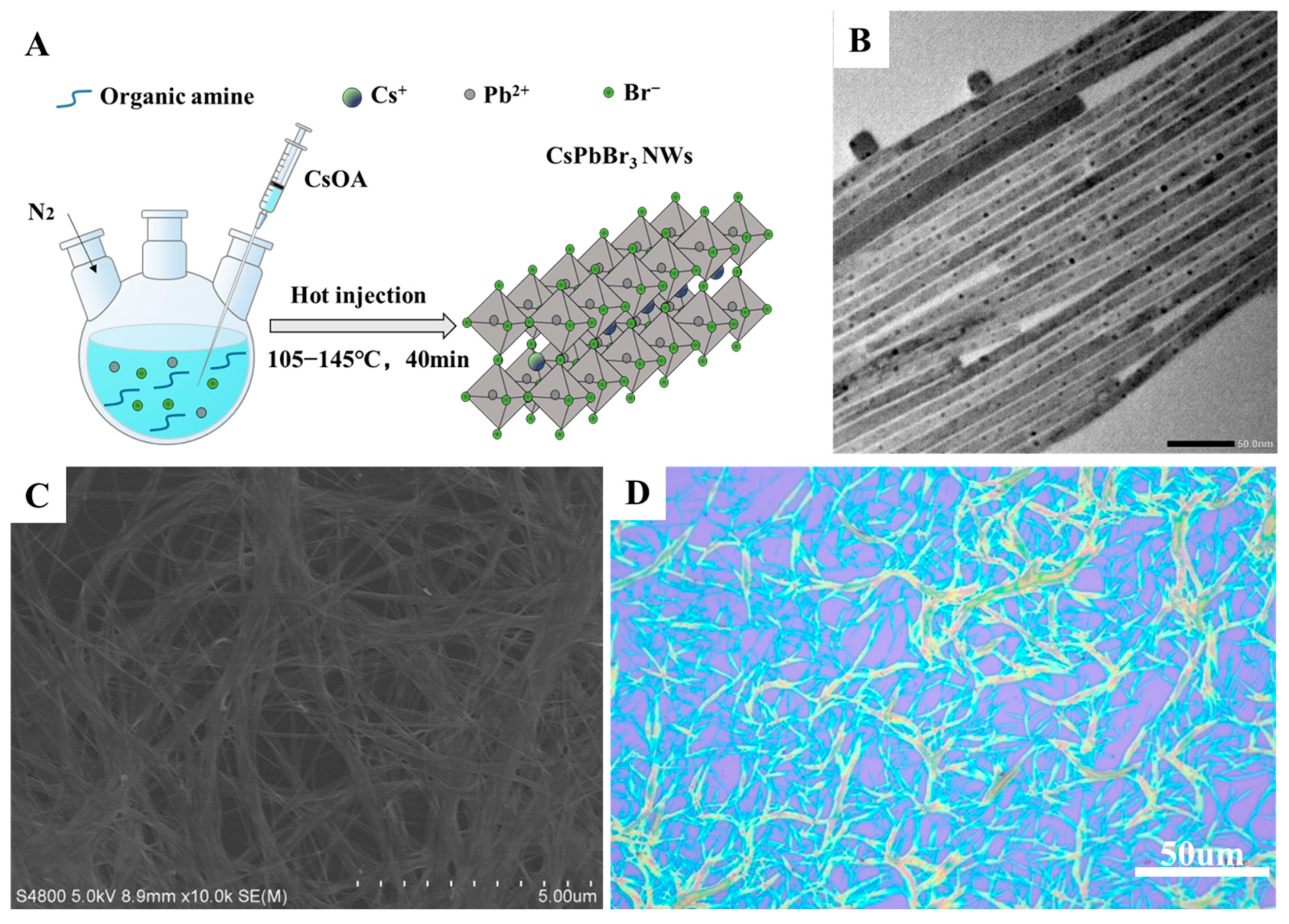
Figure 2.
(A) HAADF-STEM; (B–D) STEM-EDS mapping of Cs, Pb, and Br; (E) HRTEM image; and (F) SADE image of the CsPbBr3 NWs. Inset of (E) is a localized enlarged HRTEM image of the red box.
Figure 2.
(A) HAADF-STEM; (B–D) STEM-EDS mapping of Cs, Pb, and Br; (E) HRTEM image; and (F) SADE image of the CsPbBr3 NWs. Inset of (E) is a localized enlarged HRTEM image of the red box.
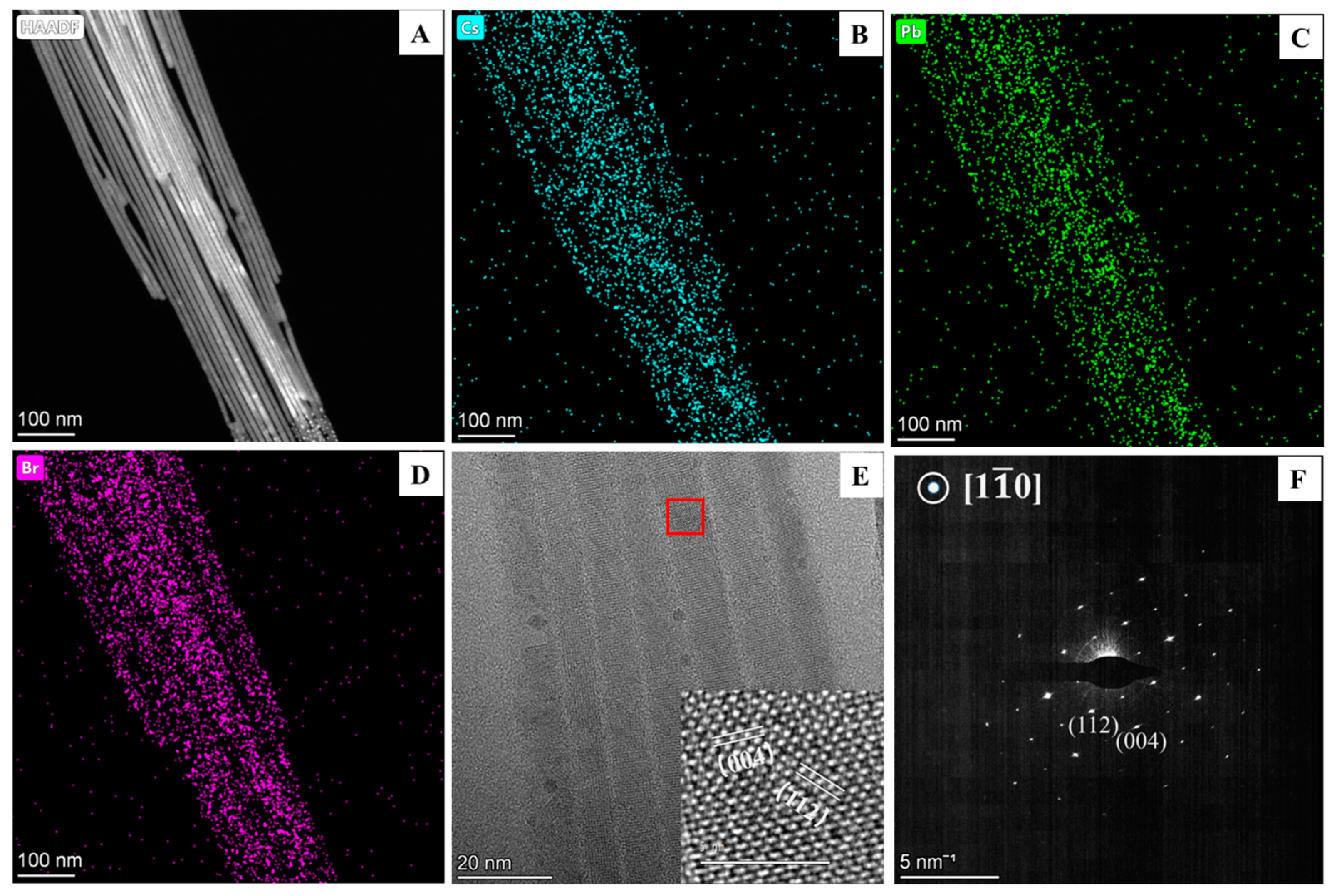
Figure 3.
(A) XRD pattern, (B) FTIR spectra, (C) full XPS spectra, and (D–F) XPS high-resolution spectra of Cs3d, Pb4f, and Br3d of the CsPbBr3 NWs.
Figure 3.
(A) XRD pattern, (B) FTIR spectra, (C) full XPS spectra, and (D–F) XPS high-resolution spectra of Cs3d, Pb4f, and Br3d of the CsPbBr3 NWs.
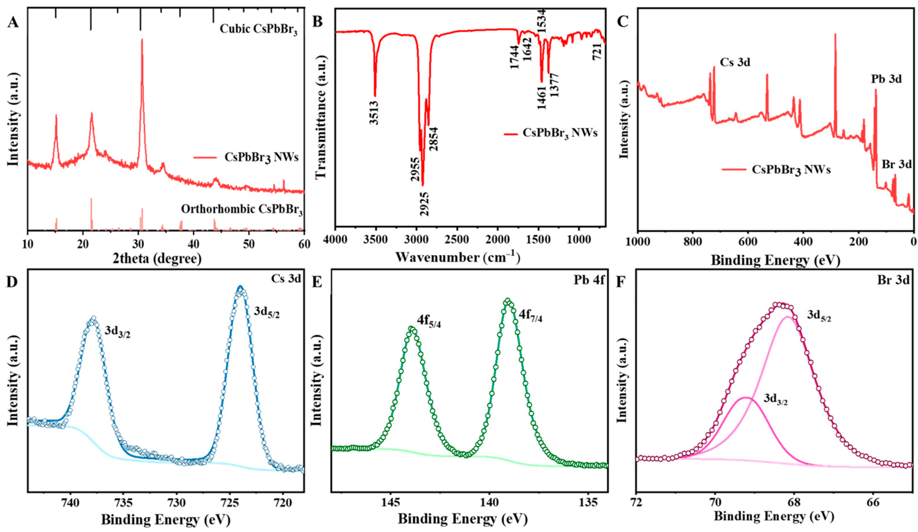
Figure 4.
(A) UV-Vis absorption and photoluminescence (PL) spectra. (B) Time-resolved photoluminescence (TRPL) spectra of the CsPbBr3 NWs. (C) Transient photocurrent responses to on–off illumination of the CsPbBr3 NWs electrodes at −0.1 V versus NHE in neutral water (0.5 M Na2SO4). (D) Electrochemical impedance spectra (Nyquist plot) of the CsPbBr3 NWs.
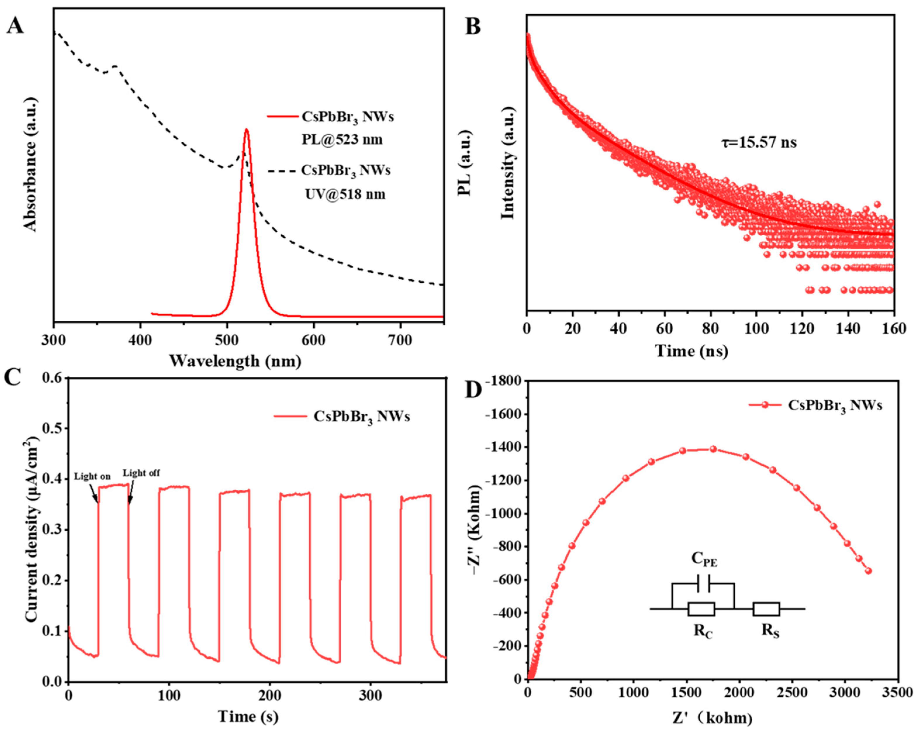
Figure 5.
(A) Schematic diagram of the anion exchange reactions all-inorganic CsPbX3 (X = Cl, Br, I) NWs. (B) Images of CsPbX3 (X = Cl, Br, I) NWs solutions under sunlight and 365 nm UV lamp, respectively. (C) UV-Vis absorption spectra and (D) photoluminescence (PL) spectra of CsPbX3 (X = Cl, Br, and I) NWs.

Disclaimer/Publisher’s Note: The statements, opinions and data contained in all publications are solely those of the individual author(s) and contributor(s) and not of MDPI and/or the editor(s). MDPI and/or the editor(s) disclaim responsibility for any injury to people or property resulting from any ideas, methods, instructions or products referred to in the content. |
© 2024 by the authors. Licensee MDPI, Basel, Switzerland. This article is an open access article distributed under the terms and conditions of the Creative Commons Attribution (CC BY) license (https://creativecommons.org/licenses/by/4.0/).
Share and Cite
MDPI and ACS Style
He, J.; Li, H.; Liu, C.; Wang, X.; Zhang, Q.; Liu, J.; Wang, M.; Liu, Y. Hot-Injection Synthesis of Cesium Lead Halide Perovskite Nanowires with Tunable Optical Properties. Materials 2024, 17, 2173. https://doi.org/10.3390/ma17102173
AMA Style
He J, Li H, Liu C, Wang X, Zhang Q, Liu J, Wang M, Liu Y. Hot-Injection Synthesis of Cesium Lead Halide Perovskite Nanowires with Tunable Optical Properties. Materials. 2024; 17(10):2173. https://doi.org/10.3390/ma17102173
Chicago/Turabian StyleHe, Jiazhen, Hang Li, Chengqi Liu, Xiaoqian Wang, Qi Zhang, Jinfeng Liu, Mingwei Wang, and Yong Liu. 2024. "Hot-Injection Synthesis of Cesium Lead Halide Perovskite Nanowires with Tunable Optical Properties" Materials 17, no. 10: 2173. https://doi.org/10.3390/ma17102173
Note that from the first issue of 2016, this journal uses article numbers instead of page numbers. See further details here.