1. Introduction
GaN-based light emitting diodes (LEDs) and laser diodes (LDs) have made huge progress in recent years [
1,
2,
3]. To further enhance the performance of optoelectronic devices, patterned sapphire substrates (PSSs) are widely used to strengthen the light extraction efficiency (LEE) and external quantum efficiency [
4,
5,
6]. The utilization of PSSs could greatly annihilate dislocations [
4,
7,
8,
9]. Interestingly, with the appropriate nucleation layer (NL), most GaN grows in the flat regions between cones, though the flat region is a rather small proportion of the whole substrate, no matter what the geometry of the pattern is [
10,
11,
12]. However, some GaN would still form small GaN crystals on the cone sidewalls, which may have negative influences on GaN growth [
13,
14]. In our previous work, we confirmed that small GaN crystals would generate dislocations [
15]. When using metal organic chemical vapor deposition (MOCVD) to grow AlN or GaN NLs, the influences of small GaN crystals become more noteworthy [
13,
14,
16]. Compared to MOCVD-grown AlN or GaN NLs, Li-Chuan Chang et al. found that the utilization of ex situ sputtered AlN NLs could suppress GaN nucleation on cones and improve the quality of GaN films on PSSs [
17]. Subsequently, many works proved that the utilization of sputtered AlN/PSS templates could improve the performance of GaN-based LEDs [
18,
19]. However, small GaN crystals on the cones’ surface of sputtered AlN/PSS templates may still deteriorate the crystal quality [
15,
20,
21]. The study of small GaN crystals on sputtered AlN/PSS templates is beneficial to further improve the crystal quality.
In this work, we deposited AlON on PSSs by sputtering AlN with small flux feeding of O2, which could improve the quality of the GaN film. We found that the thickness of the sputtered AlON NL had great influences on GaN growth. When the sputtered AlON NL was 10 nm, large crystals nucleated on the cone sidewalls, and GaN grew in non-(0001) orientation. When the sputtered AlON NL was 25 nm, small GaN crystals formed near the bottom of the cones, which merged at early stages of growth. As GaN grew on 40 nm sputtered AlON/PSS templates, GaN crystals formed at the top of the cones, and the crystals had more opportunities to grow. The disparity of the small GaN crystals on cones resulted in the different crystal quality of GaN films. After detailed characterization and analysis, we obtained the optimum thickness of sputtered AlON and illustrated the GaN growth mechanism with sputtered AlON/PSS templates.
2. Materials and Methods
The 2 in c-plane cone-shaped PSSs (bottom diameter, interval spacing, and height of the cones are 2.7, 0.2, and 1.5 μm) were prepared by inductively coupled plasma etching and photolithography. After the preparation of PSSs, AlON layers were sputtered on the substrates at 650 °C by feeding 2 sccm O2, 30 sccm Ar2, and 180 sccm N2. The thickness of AlON was based on the sputtering technique on conventional sapphire substrates (CSSs) by the mature commercial sputtering system. Before GaN growth, the sputtered AlON/PSS templates were pre-treated under an atmosphere of H2 for 5 min, and the temperature was 1100 °C. After that, the templates were cooled down to 520 °C, and the nitridation of the templates was under an atmosphere of NH3 for 3 min. Then, 5 μm GaN was grown on 10, 25, and 40 nm sputtered AlON/PSS templates. Trimethylgallium and ammonia were the precursors for Ga and N. High-purity N2 was employed as the carrier gas, and the pressure of the reaction chamber was held at 400 mBar. In the first step (900 s), the growth temperature was 970 °C, and the V/III mole ratio was 1500. In the second step (500 s), the temperature and V/III mole ratio were gradually varied to 1060 °C and 900. During the third step (4000 s), the temperature and V/III mole ratio were held at 1060 °C and 900. To further figure out the differences of the growth process between three samples, we did another group of experiments on conventional sapphire substrates (CSSs) with 10, 25, and 40 nm sputtered AlON layers. The growth condition of GaN films on CSSs remained the same as that on PSSs.
3. Results and Discussion
3.1. Charatcerization of Sputtered AlON/PSS Templates
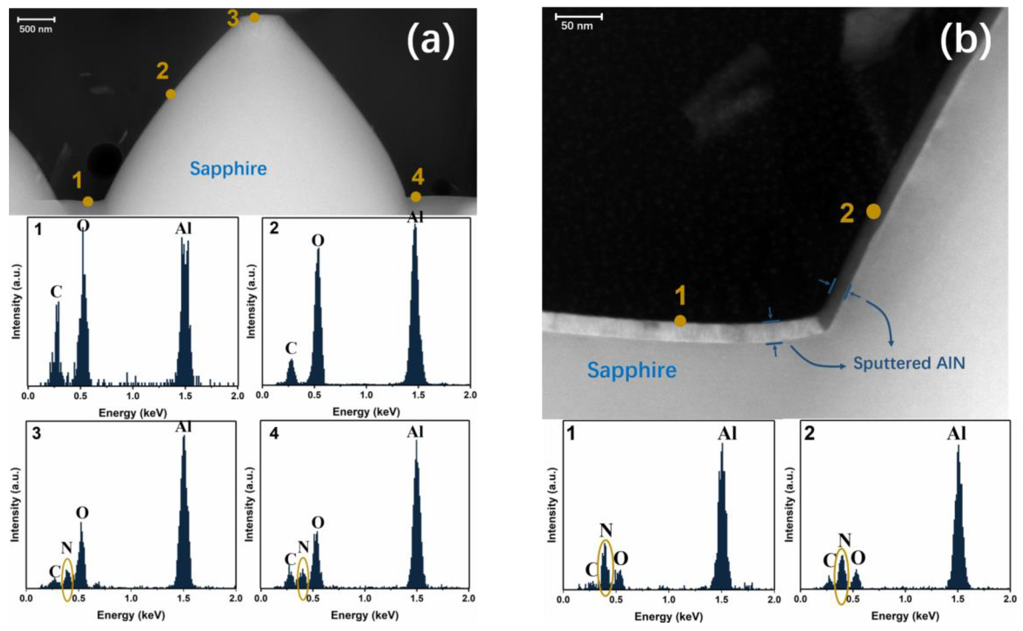
Firstly, we made a detailed characterization of 10 nm and 25 nm sputtered AlON/PSS templates. The cross-sectional transmission electron microscope (TEM) images and energy-dispersive X-ray spectroscopy (EDX) were acquired by ecnai G2 F20 S-Twin operating at 200 kV. The cross-sectional TEM and EDX results are provided in
Figure 1. We marked some spots in
Figure 1 that matched the EDX results. In
Figure 1b, the sputtered AlON layers in the flat regions and cones were 23.3 nm and 17.1 nm, respectively. The thickness of AlON was based on the standard of the sputtering technique on CSSs, so the thickness of the sputtered AlON layer on the PSS had some deviation, which was also reported by other groups [
4,
16]. The EDX results of four spots in the 10 nm sputtered AlON layer are given in
Figure 1a. Nitrogen was only found in the flat regions, which means there were no effective NLs on the cone sidewalls. As for the 25 nm sputtered AlON/PSS template, nitrogen could be found in both flat regions and the cones’ surface.
3.2. Morphology Comparation at Early Stages
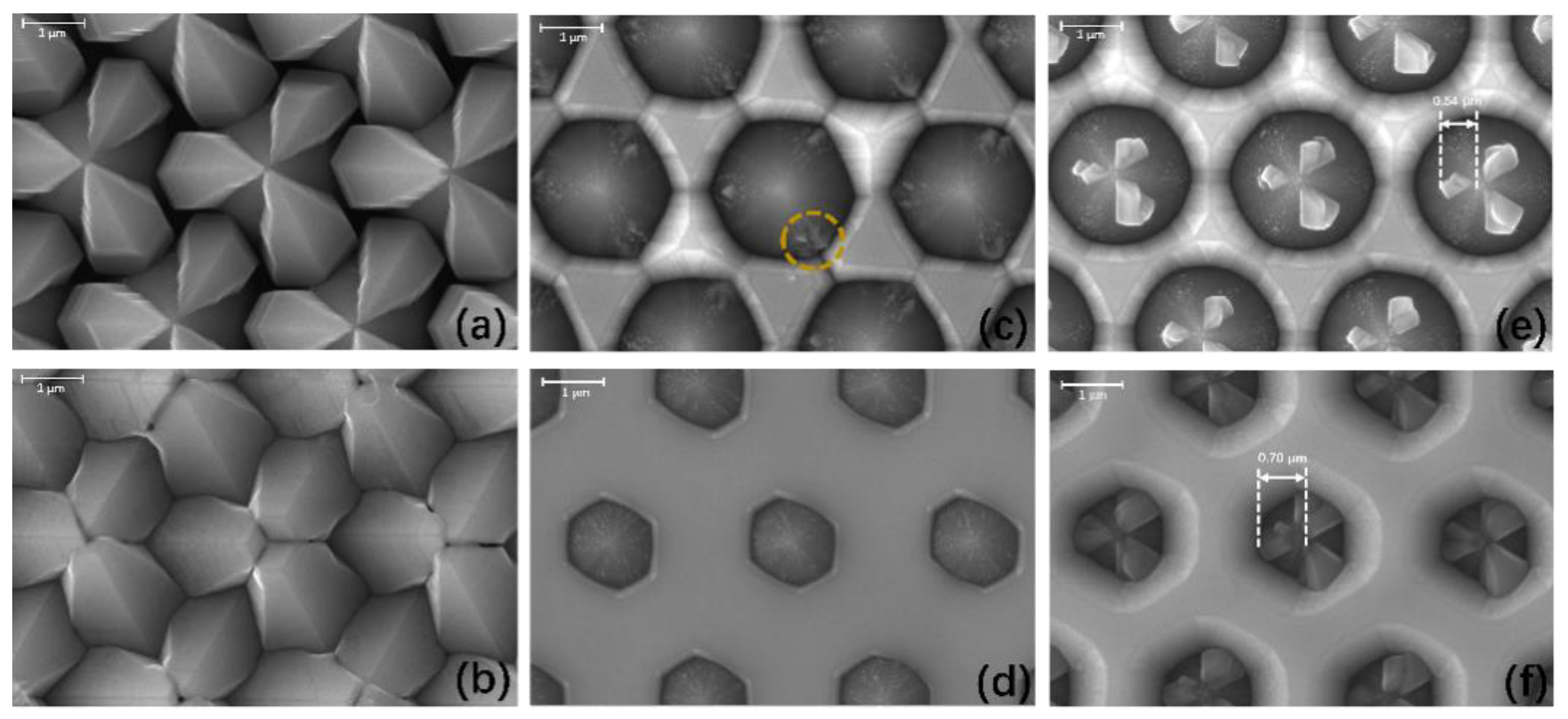
Subsequently, we obtained the morphology information of GaN films on 10, 25, and 40 nm sputtered AlON/PSS templates at two early stages, named stage 1 (200 s) and stage 2 (800 s). The top-view images were captured by FEI MLA 650F scanning electron microscope (SEM). From
Figure 2a, large GaN crystals formed on the cones, and we could not find any GaN in the flat regions, which means GaN mainly nucleated and grew on the cones. At stage 2, the collision of large GaN crystals generated many interfaces, and the GaN film could not coalesce, observed in
Figure 2b. If the thin, low-temperature MOCVD GaN NL was deposited on the PSS, or there was no NL on the cones of the PSS, GaN mostly nucleated on the cones [
6,
19,
22].
Compared with the GaN film on the 10 nm sputtered AlON/PSS template, GaN grew from the flat regions on 25 nm and 40 nm sputtered AlON/PSS templates. At stage 1, there was only small GaN on the cones, observed from
Figure 2c,e. Interestingly, the small GaN crystals on the 25 nm and 40 nm sputtered AlON/PSS templates were at different positions on the cones’ surface. Small GaN crystals in
Figure 2c were near the bottom of the cones, and they did not have a clear shape. The small GaN crystals on the 40 nm sputtered AlON/PSS template were at the top of the cones and had clearer shapes. At stage 2, small GaN crystals on the 25 nm sputtered AlON/PSS template were totally merged, but we could still see the GaN crystals on the 40 nm sputtered AlON/PSS template. The size of GaN crystals on the 40 nm sputtered AlON/PSS template increased from 0.54 μm to 0.70 μm by our measurement. It could be inferred that GaN crystals on the 40 nm sputtered AlON/PSS template had more chances to grow, and generated more dislocations [
15,
20,
21].
When the thickness of sputtered AlON turned from 25 nm to 40 nm, small GaN crystals nucleated from the bottom to the top of the cones. The thickness of sputtered AlON may have had influences on the migration ability of Ga atoms. Stronger migration ability of Ga atoms would have enhanced lateral growth, and the islands would have coalesced earlier, which has been proven in other nitride materials like AlN [
23,
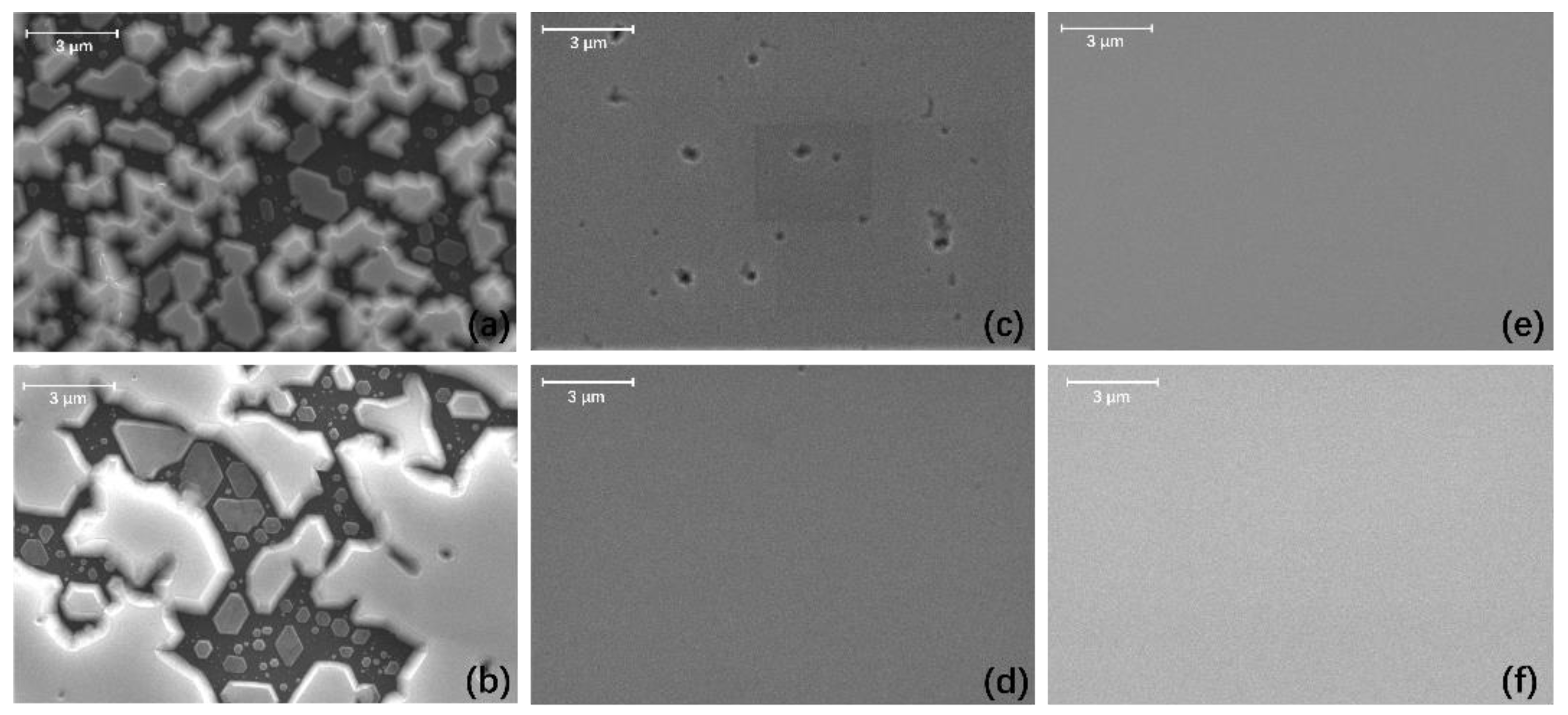
24]. Therefore, we grew GaN films on CSSs with 10, 25, and 40 nm sputtered AlON. We obtained top-view SEM images of GaN films on 10, 25, and 40 nm sputtered AlON/CSS templates at early stages in
Figure 3.
We observed that the GaN film on the 40 nm sputtered AlON/CSS template had totally coalesced at stage 1, from
Figure 3e. Compared with the GaN film on the 40 nm sputtered AlON/CSS template, there were some holes on the surface of the GaN film on the 25 nm sputtered AlON/CSS template. Therefore, GaN grown on the 40 nm sputtered AlON/CSS template coalesced earlier than that on the 25 nm sputtered AlON/CSS templates, which meant the migration ability of Ga atoms on the 40 nm sputtered AlON was stronger. Therefore, the stronger migration ability promoted Ga atoms to move to the top of the cones and form GaN. However, for sample B, the small GaN crystals could only form near the bottom of the cones because of the weaker migration ability of Ga atoms, shown in
Figure 2c,e.
In the GaN film on the 10 nm sputtered AlON/PSS template, the GaN film could not coalesce even at stage 2. Thus, we concluded that the migration ability of Ga atoms on the 10 nm sputtered AlON layer was relatively weak, compared with Ga atoms on the 25 or 40 nm sputtered AlON layers. The weak migration ability of GaN atoms on 10 nm sputtered AlON made lateral growth of GaN islands relatively slower than GaN islands on the 25 or 40 nm sputtered AlON/PSS template.
3.3. Charaterizaiton of the GaN Films
We have confirmed that the thickness variation of sputtered AlON NLs had great influences on the GaN growth on PSSs at early stages. To further discuss the GaN films, we did detailed characterization of 5 μm GaN films on 10, 25, and 40 nm sputtered AlON/PSS templates.
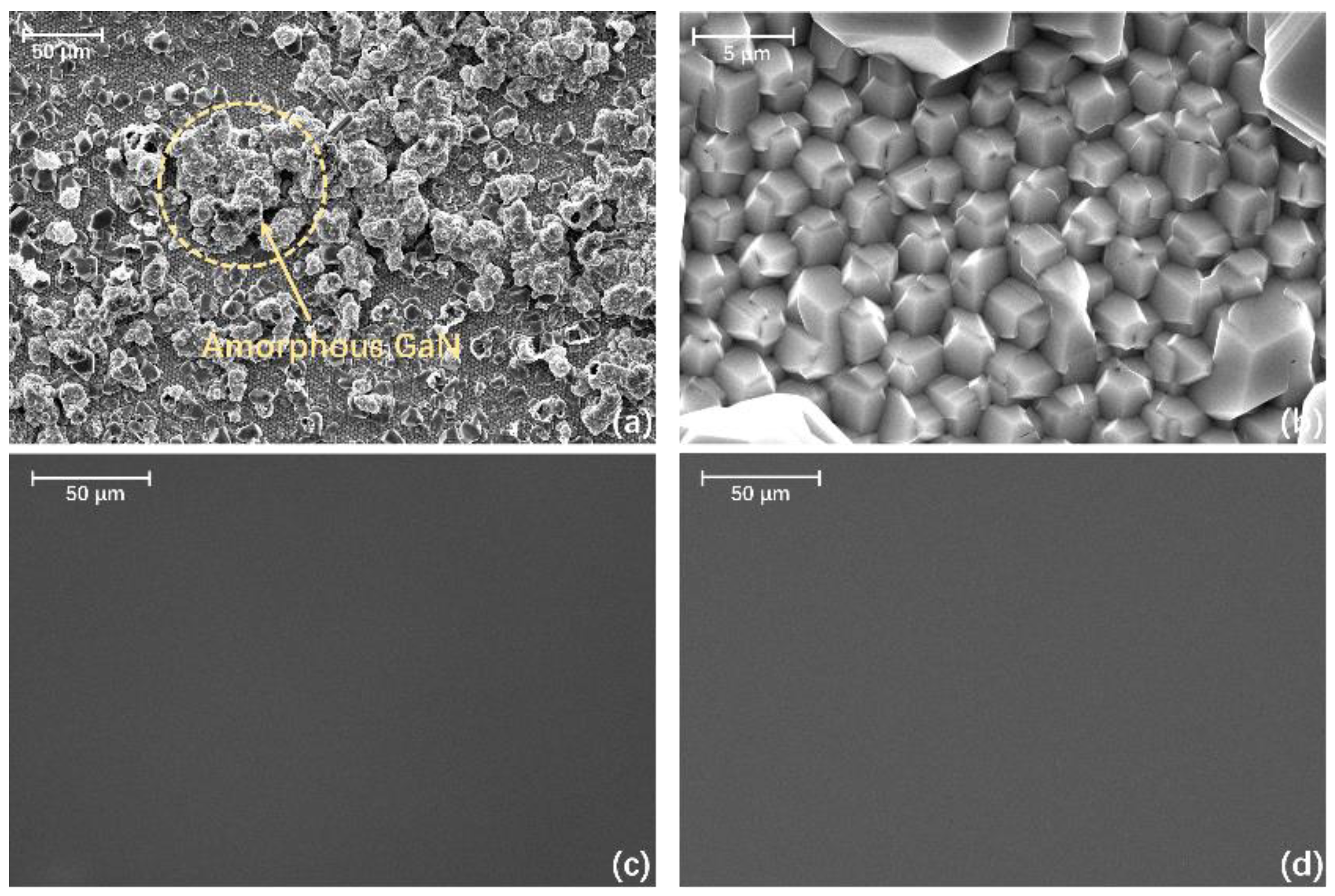
Figure 4 gives the top-view SEM images of GaN films on 10, 25, and 40 nm sputtered AlON/PSS templates. We observed that the surface of GaN films on 25 nm and 40 nm sputtered AlON/PSS templates was very smooth from
Figure 4c,d. However, for the GaN film on the 10 nm sputtered AlON/PSS template, GaN could not coalesce and some amorphous GaN formed, shown in
Figure 4b.
The cross-sectional SEM images of GaN films on 10, 25, and 40 nm sputtered AlON/PSS templates were taken from the [
11,
12,
13,
14,
15,
16,
17,
18,
19,
20] direction, presented in
Figure 5. From the cross-sectional SEM image of the GaN film on the 10 nm sputtered AlON/PSS template, we could clearly observe that GaN could not coalesce well. In
Figure 5a, we saw that there were voids between the cones, and the interfaces resulted from the collision of GaN crystals. As for GaN films on 25 nm and 40 nm sputtered AlON/PSS templates, there were no hollows or cracks.
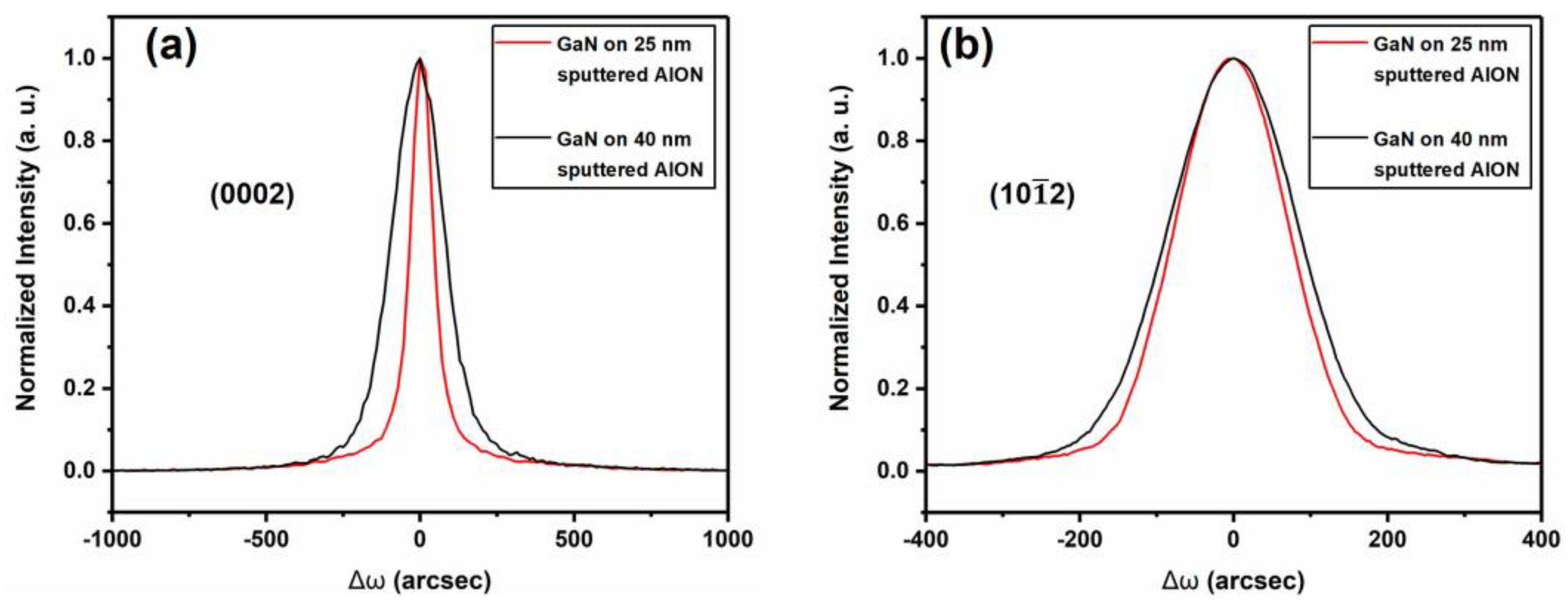
Although the morphology of GaN films on the 25 nm and 40 nm sputtered AlON/PSS was very smooth, we considered that the crystal quality of the GaN film on the 40 nm sputtered AlON/PSS would be inferior to that on the 25 nm sputtered AlON/PSS template, for the larger GaN crystals on the cone sidewalls generated more dislocations. To verify our analysis, we characterized the crystal quality of GaN films on 10, 25, and 40 nm sputtered AlON/PSS templates by Bruker D8 high-resolution X-ray diffraction (HRXRD). The full width at half maximum (FWHM) of the ω-scan rocking curve at the symmetric (0002) and (10
2) plane can reflect the dislocation density [
25,
26]. Because the quality of sample A was severely deteriorated, the rocking curve of sample A could not be obtained.
Figure 6 and
Table 1 give the ω-scan rocking curve and calculated dislocations of GaN films on 25 nm and 40 nm sputtered AlON/PSS templates.
FWHM results of the ω-scan rocking curve at the symmetric (0002)/(10
2) planes of GaN films on 25 nm and 40 nm sputtered AlON/PSS templates were 87/149 arcsec and 196/169 arcsec, respectively. The calculated dislocation densities of GaN films on 25 nm and 40 nm sputtered AlON/PSS templates are presented in
Table 1. The density of total dislocations in the GaN film on the 40 nm sputtered AlON/PSS template was about 70% higher than that in the GaN film on the 25 nm sputtered AlON/PSS template. Thus, we concluded that when GaN grew on the 40 nm sputtered AlON/PSS templates, the larger crystals at the top of the cones generated more dislocations.
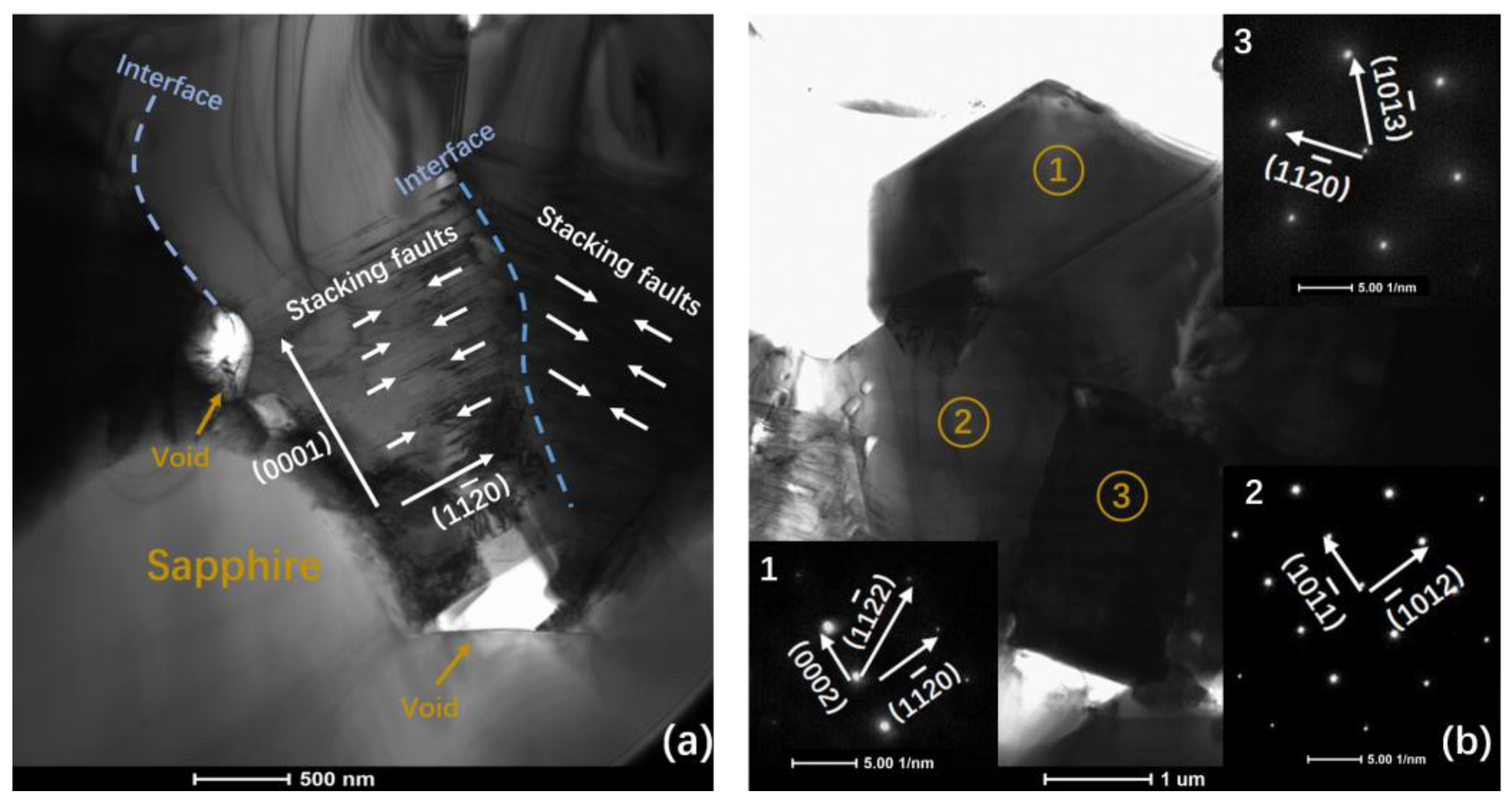
The growth process of the GaN film on 10 nm sputtered AlON/PSS was complicated, so we used cross-sectional TEM to further determine the characteristics.
Figure 7 provides detailed information of the GaN film on 10 nm sputtered AlON/PSS, and selected-area electron diffraction (SAED) patterns are also presented. From
Figure 7a, we could clearly see that GaN nucleated on the cones. GaN grew larger from the cones’ surface and collided with each other. The slope of the sapphire cones allowed for tilted nucleation of a-plane GaN similar to a-plane growth on r-plane sapphire [
27]. The stacking faults indicated that GaN on the cone sidewalls presented a-plane orientation [
28,
29,
30,
31]. We observed that there were some semi-polar and non-polar planes in sample A, by our calculation from SAED patterns in
Figure 7b.
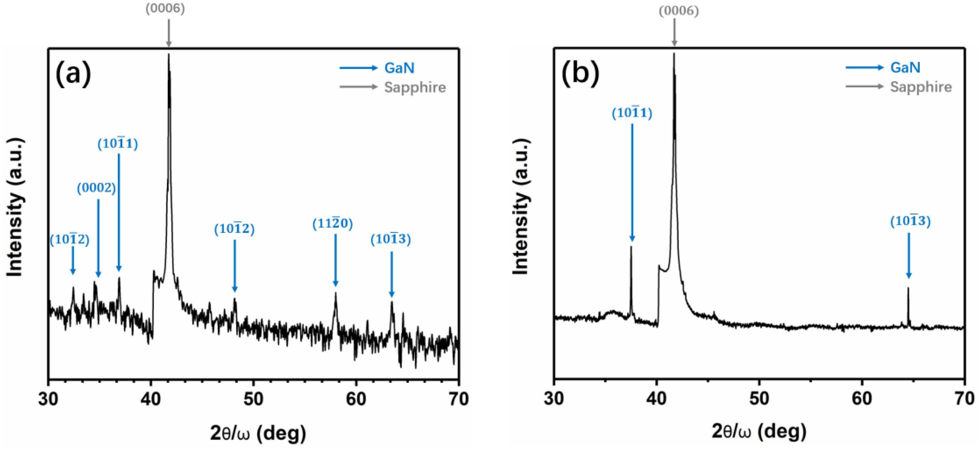
We performed a symmetric (0004) 2θ/ω powder XRD characterization for sample A to verify of our SAED calculation by Bruker D8 advance ECO, shown in
Figure 8. We inferred that GaN grew in non-(0001) orientation. The powder XRD results of the GaN film on the 10 nm sputtered AlON/PSS matched the calculation results from SAED patterns.
3.4. GaN Growth Mechanisms on Sputtered AlON/PSS Templates
Because there were no effective NLs on the cones of the 10 nm sputtered AlON/PSS, GaN mostly nucleated on the cones and formed large non-(0001) GaN crystals under the experimental conditions. As the growth proceeded, GaN crystals grew larger and collided with each other, which generated many interfaces. GaN could not coalesce and some amorphous GaN appeared.
If the sputtered AlON was 25 nm, GaN nucleated in the flat regions, and the coalescent process was successful. However, some Ga atoms inevitably transferred to the cones and formed small GaN crystals. Compared with 40 nm sputtered AlON/PSS templates, the small GaN crystals were near the bottom of the cones. Small GaN crystals merged in a short time of growth, which is shown in
Figure 2d. Moreover, the small GaN crystals on cones had fewer chances to grow larger and generate dislocations.
For GaN film grown on the 40 nm sputtered AlON/PSS template, the strong migration ability on 40 nm sputtered AlON/PSS templates meant GaN crystals could nucleate at the top the cones. Therefore, it needed more time for the small GaN crystals to merge and have more chances to grow and generate dislocations.
4. Conclusions
In this paper, we systematically discussed the differences of GaN growth mechanisms on PSSs with sputtered AlON NLs of different thickness. When the sputtered AlON was 10 nm, there were no effective sputtered AlON layers on the cones’ surface. Large non-(0001) GaN crystals nucleated on the cones, and they could not coalesce during growth. When the thickness of the sputtered AlON NL was 25 nm or 40 nm, GaN mainly grew from the flat regions, and only small GaN crystals formed on the cones’ surface. Our experiment on sputtered AlON/CSS templates showed that the migration ability of Ga atoms on the 40 nm sputtered AlON NL was stronger than that on the 25 nm sputtered AlON NL. Therefore, compared with GaN film on the 25 nm sputtered AlON/PSS template, the small GaN crystals on 40 nm sputtered AlON/PSS templates formed at the top of the cones, which had more time to grow and generate more dislocations. The larger GaN crystals on 40 nm sputtered AlON/PSS templates deteriorated the crystal quality of the GaN film. Finally, we gave the mechanisms of GaN growth on sputtered AlON/PSS templates, as the thickness of sputtered AlON varied from 10 nm to 40 nm.
Author Contributions
Experiment, analysis, and writing, Y.G.; Conceiving the idea, review and editing, S.X., J.Z. and Y.H.; Characterization, R.P. and H.T.; Funding supported, S.X., J.Z. and Y.H. All authors have read and agreed to the published version of the manuscript.
Funding
This research is supported by the National Key Research and development Program of China (Grant No. 2018YFB0406601), the National Natural Science Foundation of China (Grant No. 61574108, 61334002, 61474086, 51302306), and the Fundamental Research Funds for the Central Universities, and by the Innovation Fund of Xidian University.
Conflicts of Interest
The authors declare no conflict of interest.
References
- Xiong, F.; Guo, W.; Feng, S.; Li, X.; Du, Z.; Wang, L.; Deng, J.; Sun, J. Transfer-Free Graphene-Like Thin Films on GaN LED Epiwafers Grown by PECVD Using an Ultrathin Pt Catalyst for Transparent Electrode Applications. Materials 2019, 12, 3533. [Google Scholar] [CrossRef] [Green Version]
- Wang, Y.; Li, P.; Zhang, X.; Xu, S.; Zhou, X.; Wu, J.; Yue, W.; Hao, Y. Using a Multi-Layer Stacked AlGaN/GaN Structure to Improve the Current Spreading Performance of Ultraviolet Light-Emitting Diodes. Materials 2020, 13, 454. [Google Scholar] [CrossRef] [Green Version]
- Chen, S.-W.; Li, H.; Chang, C.-J.; Lu, T.-C. Effects of Nanoscale V-Shaped Pits on GaN-Based Light Emitting Diodes. Materials 2017, 10, 113. [Google Scholar] [CrossRef] [Green Version]
- Chen, C.-C.; Yap, C.-Y.; Hsu, W.-Y.; Kuo, C.-T.; Tsai, T.-L.; Chu, J.-Y.; Wu, Y.C.S. Crystal Quality and Light Output Power of GaN-Based LEDs Grown on Nanoporous Patterned Sapphire Substrate. ECS Solid State Lett. 2014, 3, R45–R47. [Google Scholar] [CrossRef] [Green Version]
- Lee, J.-H.; Oh, J.T.; Kim, Y.C.; Lee, J.-H. Stress Reduction and Enhanced Extraction Efficiency of GaN-Based LED Grown on Cone-Shape-Patterned Sapphire. IEEE Photon. Technol. Lett. 2008, 20, 1563–1565. [Google Scholar] [CrossRef]
- Kim, J.B.; Kim, S.-M.; Kim, Y.-W.; Kang, S.-K.; Jeon, S.R.; Hwang, N.; Choi, Y.-J.; Chung, C.S. Light Extraction Enhancement of GaN-Based Light-Emitting Diodes Using Volcano-Shaped Patterned Sapphire Substrates. Jpn. J. Appl. Phys. 2010, 49, 42102. [Google Scholar] [CrossRef]
- Xu, S.; Li, P.; Zhang, J.; Jiang, T.; Ma, J.; Lin, Z.; Hao, Y. Threading dislocation annihilation in the GaN layer on cone patterned sapphire substrate. J. Alloys Compd. 2014, 614, 360–363. [Google Scholar] [CrossRef]
- Wuu, D.-S.; Wu, H.-W.; Chen, S.-T.; Tsai, T.-Y.; Zheng, X.; Horng, R.-H. Defect reduction of laterally regrown GaN on GaN/patterned sapphire substrates. J. Cryst. Growth 2009, 311, 3063–3066. [Google Scholar] [CrossRef]
- Jeon, D.-W.; Cho, H.-S.; Park, J.-W.; Jang, L.-W.; Kim, M.; Jeon, J.-W.; Ju, J.-W.; Baek, J.H.; Lee, I.-H. Separation of laterally overgrown GaN template by using selective electrochemical etching. J. Alloys Compd. 2012, 542, 59–62. [Google Scholar] [CrossRef]
- Zhou, S.; Lin, Z.; Wang, H.; Qiao, T.; Zhong, L.; Lin, Y.; Wang, W.; Yang, W.; Li, G. Nucleation mechanism for epitaxial growth of GaN on patterned sapphire substrates. J. Alloys Compd. 2014, 610, 498–505. [Google Scholar] [CrossRef]
- Lee, J.-H.; Lee, D.-Y.; Oh, B.-W.; Lee, J.-H. Comparison of InGaN-Based LEDs Grown on Conventional Sapphire and Cone-Shape-Patterned Sapphire Substrate. IEEE Trans. Electron Devices 2009, 57, 157–163. [Google Scholar] [CrossRef]
- Song, J.-C.; Lee, S.-H.; Lee, I.-H.; Seol, K.-W.; Kannappan, S.; Lee, C.-R. Characteristics comparison between GaN epilayers grown on patterned and unpatterned sapphire substrate (0001). J. Cryst. Growth 2007, 308, 321–324. [Google Scholar] [CrossRef]
- Kim, Y.H.; Ruh, H.; Noh, Y.K.; Kim, M.-D.; Oh, J.E. Microstructural properties and dislocation evolution on a GaN grown on patterned sapphire substrate: A transmission electron microscopy study. J. Appl. Phys. 2010, 107, 063501–063505. [Google Scholar] [CrossRef]
- Chen, Y.; Chen, Z.; Li, J.; Chen, Y.; Li, C.; Zhan, J.; Yu, T.; Kang, X.; Jiao, F.; Li, S.; et al. A study of GaN nucleation and coalescence in the initial growth stages on nanoscale patterned sapphire substrates via MOCVD. CrystEngComm 2018, 20, 6811–6820. [Google Scholar] [CrossRef]
- Peng, R.; Hao, Y.; Meng, X.; Xu, S.; Zhang, J.; Li, P.; Huang, J.; Du, J.; Zhao, Y.; Fan, X. Study on Dislocation Annihilation Mechanism of the High-Quality GaN Grown on Sputtered AlN/PSS and Its Application in Green Light-Emitting Diodes. IEEE Trans. Electron Devices 2019, 66, 2243–2248. [Google Scholar] [CrossRef]
- Hu, H.; Zhou, S.; Liu, X.; Gao, Y.; Gui, C.; Liu, S. Effects of GaN/AlGaN/Sputtered AlN nucleation layers on performance of GaN-based ultraviolet light-emitting diodes. Sci. Rep. 2017, 7, 44627–44637. [Google Scholar] [CrossRef]
- Chang, L.-C.; Chen, Y.-A.; Kuo, C.-H. Spatial Correlation Between Efficiency and Crystal Structure in GaN-Based Light-Emitting Diodes Prepared on High-Aspect Ratio Patterned Sapphire Substrate With Sputtered AlN Nucleation Layer. IEEE Trans. Electron Devices 2014, 61, 2443–2447. [Google Scholar] [CrossRef]
- Chen, S.-W.; Li, H.; Lu, T.-C. Improved performance of GaN based light emitting diodes with ex-situ sputtered AlN nucleation layers. AIP Adv. 2016, 6, 045311–045317. [Google Scholar] [CrossRef]
- Lai, W.C.; Yen, C.H.; Yang, Y.Y.; Wang, C.K.; Chang, S.J. GaN-Based Ultraviolet Light Emitting Diodes With Ex Situ Sputtered AlN Nucleation Layer. J. Disp. Technol. 2013, 9, 895–899. [Google Scholar] [CrossRef]
- Wu, P.-Y.; Li, J.-H.; Hsu, L.-H.; Huang, C.-Y.; Cheng, Y.-J.; Kuo, H.-C.; Wu, Y.S. Effect of Sputtered AlN Location on the Growth Mechanism of GaN. ECS J. Solid State Sci. Technol. 2017, 6, R131–R134. [Google Scholar] [CrossRef]
- He, C.; Zhao, W.; Zhang, K.; He, L.; Wu, H.; Liu, N.; Zhang, S.; Liu, X.; Chen, Z. High-Quality GaN Epilayers Achieved by Facet-Controlled Epitaxial Lateral Overgrowth on Sputtered AlN/PSS Templates. ACS Appl. Mater. Interfaces 2017, 9, 43386–43392. [Google Scholar] [CrossRef]
- Shang, L.; Zhai, G.; Mei, F.; Jia, W.; Yu, C.; Liu, X.-G.; Xu, B. The effect of nucleation layer thickness on the structural evolution and crystal quality of bulk GaN grown by a two-step process on cone-patterned sapphire substrate. J. Cryst. Growth 2016, 442, 89–94. [Google Scholar] [CrossRef]
- Nitta, S.; Yukawa, Y.; Watanabe, Y.; Kamiyama, S.; Amano, H.; Akasaki, I. Mass Transport of AlxGa1—xN. Phys. Status Solidi (A) 2002, 194, 485–488. [Google Scholar] [CrossRef]
- Jain, R.; Sun, W.; Yang, J.; Shatalov, M.; Hu, X.; Sattu, A.; Lunev, A.; Deng, J.; Shturm, I.; Bilenko, Y.; et al. Migration enhanced lateral epitaxial overgrowth of AlN and AlGaN for high reliability deep ultraviolet light emitting diodes. Appl. Phys. Lett. 2008, 93, 051113. [Google Scholar] [CrossRef]
- Shen, X.-Q.; Matsuhata, H.; Okumura, H. Reduction of the threading dislocation density in GaN films grown on vicinal sapphire (0001) substrates. Appl. Phys. Lett. 2005, 86, 21912–21915. [Google Scholar] [CrossRef]
- Moram, M.A.; Vickers, M.E. X-ray diffraction of III-nitrides. Rep. Prog. Phys. 2009, 72, 36502. [Google Scholar] [CrossRef]
- Leung, B.; Sun, Q.; Yerino, C.D.; Han, J.; Coltrin, M.E. Using the kinetic Wulff plot to design and control nonpolar and semipolar GaN heteroepitaxy. Semicond. Sci. Technol. 2012, 27, 24005. [Google Scholar] [CrossRef]
- Cho, Y.S.; Sun, Q.; Lee, I.-H.; Ko, T.-S.; Yerino, C.D.; Han, J.; Kong, B.H.; Cho, H.K.; Wang, S. Reduction of stacking fault density in m-plane GaN grown on SiC. Appl. Phys. Lett. 2008, 93, 111904. [Google Scholar] [CrossRef]
- Johnston, C.; Kappers, M.; Moram, M.; Hollander, J.; Humphreys, C. Assessment of defect reduction methods for nonpolar a-plane GaN grown on r-plane sapphire. J. Cryst. Growth 2009, 311, 3295–3299. [Google Scholar] [CrossRef]
- Fischer, A.M.; Wu, Z.; Sun, K.; Wei, Q.Y.; Huang, Y.; Senda, R.; Lida, D.; Iwaya, M.; Amano, H.; Ponce, F.A. Misfit Strain Relaxation by Stacking Fault Generation in InGaN Quantum Wells Grown on m-plane GaN. Appl. Phys. Express. 2009, 2, 041002. [Google Scholar] [CrossRef]
- Bai, J.; Jiu, L.; Gong, Y.; Wang, T. Non-Polar (11-20) GaN grown on sapphire with double overgrowth on micro-rod/stripe templates. Semicond. Sci. Technol. 2018, 33, 125023. [Google Scholar] [CrossRef] [Green Version]
© 2020 by the authors. Licensee MDPI, Basel, Switzerland. This article is an open access article distributed under the terms and conditions of the Creative Commons Attribution (CC BY) license (http://creativecommons.org/licenses/by/4.0/).
