1. Introduction
Amorphous metal oxide semiconductors (AMOS) are attractive candidate materials for fabricating next-generation thin film transistors (TFTs), which can be used as the driving backplanes of active matrix liquid-crystal displays (AMLCD) and active matrix organic light-emitting diode (AMOLED) displays, due to their low-temperature process, high optical transparency in the visible region, high field effective mobility, low subthreshold swing, and high on/off current ratio [
1,
2]. Especially, amorphous In-Ga-Zn-O (a-IGZO) has been achieved in commercial application of AMLCD or AMOLED products. With the advances in display technology, demands for large-size and high-resolution display products are increasing. The fabrication of miniaturized TFT with the back-channel-etch (BCE) technique can meet the demands of large-size and high-resolution display panels. However, the development of miniaturized AMOS TFTs is sluggish because oxide semiconductors are sensitive to weak acid etchant, causing damage to the back-channel surface of the device. Thus, exploiting an acid-resistant and stable active layer material is one potential solution for fabricating BCE typed TFTs. Various kinds of oxide semiconductors have sprung up and been widely researched in order to achieve an excellent device performance since a-IGZO was reported [
3,
4]. Among these oxide semiconductors, tin oxide (SnO
2), with high chemical stability, low cost, and nontoxicity, was proposed as one of the promising candidates for fabricating BCE typed devices to enable high resolution [
5,
6]. However, due to polycrystalline structure and high carrier concentration of the intrinsic SnO
2, the application of TFT backplane is limited. Recently, the doping element of silicon (Si) was successfully demonstrated to be an excellent carrier suppressor in oxide semiconductors that were used for electron injection/transport of OLED [
7], the formation of Schottky contact in IGZO-TFT [
8], and the active layers in oxide TFTs [
9]. It is well known that the charge carriers in the oxide semiconductors can be related to the oxygen vacancy. For SnO
2, the oxygen vacancy can be suppressed by the Si element because oxygen bond-dissociation energy of Si-O (799.6 kJ/mol) is stronger than that of Sn-O (531.8 kJ/mol), which can prevent the oxygen atoms from getting out of the SnO
2 film during the sputtering or annealing process [
10,
11,
12].
For integrated circuit applications of oxide TFTs, the passivation layer plays a critical role in protecting devices from surroundings. Generally, oxide semiconductors are susceptible to oxygen or water molecules in the ambient atmosphere. The adsorption/desorption dynamic of O
2 or H
2O molecules on the back-channel region of the device affects the properties of oxide TFT [
13]. The adsorbed oxygen captures electrons from the channel layer, which results in a positive V
th shift in oxide TFTs (
). The absorbed water molecules can be charged and generate excess electrons into the channel layer, which leads to a negative V
th shift in oxide TFTs (
). Up until now, different species of organic and inorganic passivation layers, such as perfluoro (1-butenyl vinyl ether) polymer (CYTOP) [
14], silicon nitride (SiN
x) [
15], and silicon oxide (SiO
x) [
16] have been widely studied. The diffusion barrier properties against O
2 and H
2O molecules in the ambient of organic passivation layers are lower than that of inorganic passivation layers on account of their high permeability of ambient gas. Although the diffusion barrier properties of SiN
x against O
2 and H
2O molecules in the ambient are better than that of SiO
x, the generation of hydrogen concentration in SiN
x is higher than that of SiO
x during the deposition by plasma enhanced chemical vapor deposition (PECVD), which can deteriorate device performance and stability [
17].
In this paper, comparison of the electrical characteristics of BCE typed a-STO TFTs, with and without thermal annealing before deposition of SiOx, was carried out. It demonstrated that the pre-annealing was an important step for enhancing electrical properties of the device. The reason for achieving good electrical properties of a-STO TFTs with SiOx passivation was investigated in detail.
2. Materials and Methods
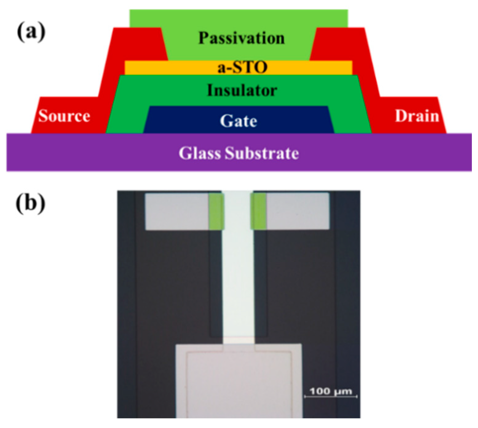
The cross-sectional configuration schematic of a-STO TFTs with BCE structure was fabricated on glass substrates, as illustrated in
Figure 1. First, a 300 nm thick Al-Nd alloy (3 wt% of Nd) was deposited on glass substrate and patterned as a gate electrode. Second, a 200 nm thick gate insulator layer of AlO
x-Nd was formed using the anodization process. Third, an ultra-thin 5 nm a-STO film was deposited by using a ceramic target (SiO
2:SnO
2 = 5:95 wt%) with a power of 300 W, an argon/oxygen flow ratio of 20/2 sccm and a pressure of 2 mtorr at room temperature, and patterned by a lift-off process. Fourth, a 200 nm Mo film used for the Source/Drain (S/D) electrodes was sputtered at room temperature and the channel width/length (100/50 μm) was defined using the wet etch process. Fifth, the passivation-free Device A was fabricated. Finally, two passivation process approaches of 300 nm SiO
x deposited by PECVD at 300 °C were conducted, respectively. A layer of SiO
x film was directly deposited on the top of Device A, which was called Device B. The channel region of Device A was covered by a SiO
x layer after being annealed at 350 °C in air ambient for 0.5 h, which resulted in the formation of Device C (See
Figure S1).
Metal electrodes were prepared by direct current (DC) magnetron sputtering and a-STO films were deposited by radio frequency (RF) Magnetron sputtering (Kurt J. Lesker, Jefferson Hills, MA, USA). Morphology and roughness of a-STO film deposited on the glass substrate were obtained by atomic force microscope (AFM, Multimode 8, Bruker, Karlsruhe, Germany) measurement. The density and thickness were analyzed by X-ray reflectivity (XRR, EMPYREAN, PANalytical, Almelo, The Netherlands). The oxygen vacancies of the channel layer were measured by X-ray photoelectron spectroscopy (XPS, Escalab 250XI, Thermo Scientific, Waltham, MA, USA). The electrical characteristics and stability of device under gate bias stress were measured in air ambient by an Agilent 4155C semiconductor parameter analyzer (Agilent, Santa Clara, CA, USA). The applied positive bias stress (PBS) and negative bias stress (NBS) were as follows: VGS = ±20 V and VDS = 0 V, which was applied for 3600 s. The transfer characteristic curves of the device were tested when the gate biases were interrupted at fixed times. Vth was extracted from the linear extrapolation of the plot of the square root of the drain current with gate voltage. And the recovery of Vth was also investigated in the dark after bias stress for 3600 s. The transfer characteristic curves of TFT were measured after 1200 s intervals. Capacitance–voltage (C–V) curves of a-STO TFTs were measured by a KEYSIGHT E4990A Impedance Analyzer (Keysight Technologies Inc., Santa Rosa, CA, USA) with a fixed frequency of 10 k Hz. The 2D device simulator ATLAS (Silvaco Inc., Santa Clara, CA, USA) was used for device simulation.
3. Results and Discussion
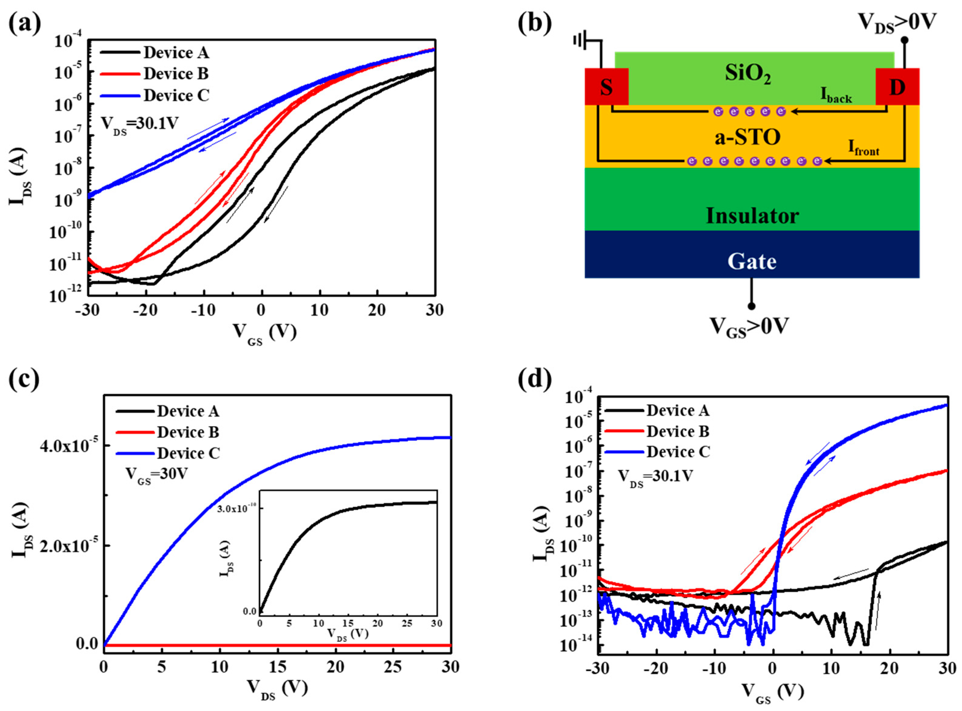
Figure 2a shows the representative transfer characteristic curves (I
DS–V
GS) of as-deposited a-STO TFTs. There were many intrinsic defects at the semiconductor/insulator interface or in the a-STO active layer film for as-deposited Device A, which led to the generation of poor electrical performance, such as a large subthreshold swing (SS) and a large hysteresis. An evident increase of OFF current (I
off) and negative shift of turn-on voltage (V
on) were found after the channel region of the device was covered by a SiO
x passivation layer. Generally, the channel current (I
front) of the device cannot be affected by a passivation layer [
18]. Thus, the increase of I
off in the passivated device was attributed to the byproduct hydrogen during the deposition of SiO
x. Because neutral H
0 could migrate in the channel layer and further react with O
2− to form OH
− and generate excessive electrons (
), which would result in the formation of back-channel current (I
back), as shown in
Figure 2b [
19].
To obtain good performance of a-STO TFTs, an additional thermal post-annealing in argon ambient for devices was inevitably carried out. The I–V curves of both Device A (~10
−10 A) and Device B (~10
−8 A) were approximate to a horizontal line compared with that of device C (~10
−5 A), as illustrated in
Figure 2c.
Figure 2d exhibits the transfer characteristic curves of devices with thermal post-annealing. The transfer characteristics of Device A and Device B were not improved by post-annealing. The channel layer of Device A was terribly transformed into an insulator-like layer. For the transfer curve of Device B, the hysteresis unexpectedly was still maintained and the reduction of ON current (I
on) also occurred. Fortunately, a good device performance was successfully achieved in Device C. The field-effect mobility in the saturation region of the device and the subthreshold swing (SS) were extracted by using the following equations [
1]:
where I
DS is the drain current, V
DS is the drain voltage, V
GS is the gate voltage, V
th is the threshold voltage, W/L is the channel width/length, and C
i is the gate capacitance per unit area of the insulator layer, respectively. The electrical parameters of devices with the post-annealing process, including saturation mobility (μ
sat), turn-on voltage (V
on), on/off current ratio (I
on/I
off), and subthreshold swing (SS) were listed in
Table 1. A large μ
sat of 4.2 ± 0.2 cm
2/V s, a low V
on of 0.00 V, a large I
on/I
off of 6.94 × 10
8, and a low SS of 0.23 V/decade were obtained in Device C.
The results of device performance implied that the pre-annealing played an important role in affecting the electrical properties of passivated device. An in-depth investigation of the thermal pre-annealing for Device A was performed.
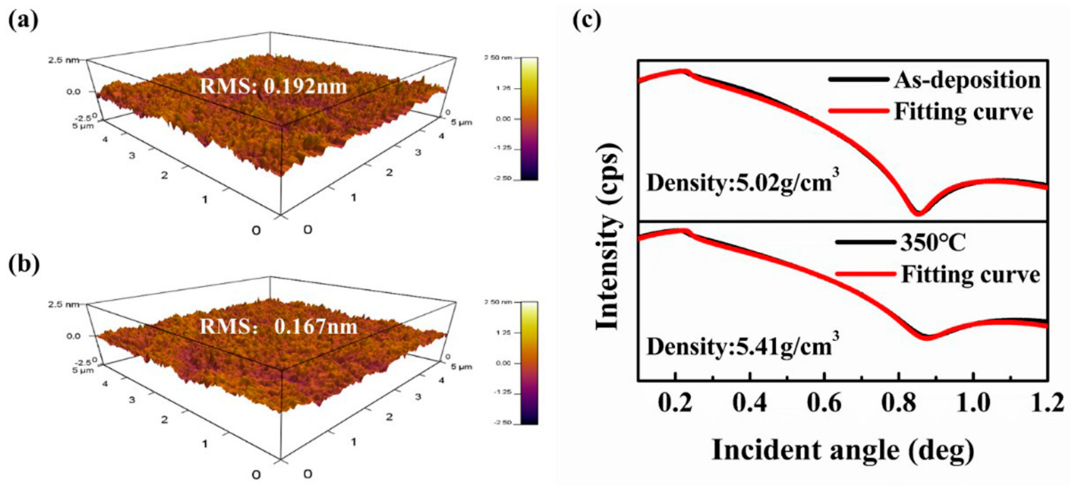
Figure 3 shows AFM images and XRR curves of 5 nm a-STO films. After a-STO film was annealed at 350 °C in air ambient for 0.5 h, the roughness reduced from 0.192 nm to 0.167 nm, while the density of a-STO film increased from 5.02 g/cm
3 to 5.41 g/cm
3. The thermal annealing process could facilitate the atoms’ rearrangement and structural relaxation to reduce internal defects and improve the quality of film.
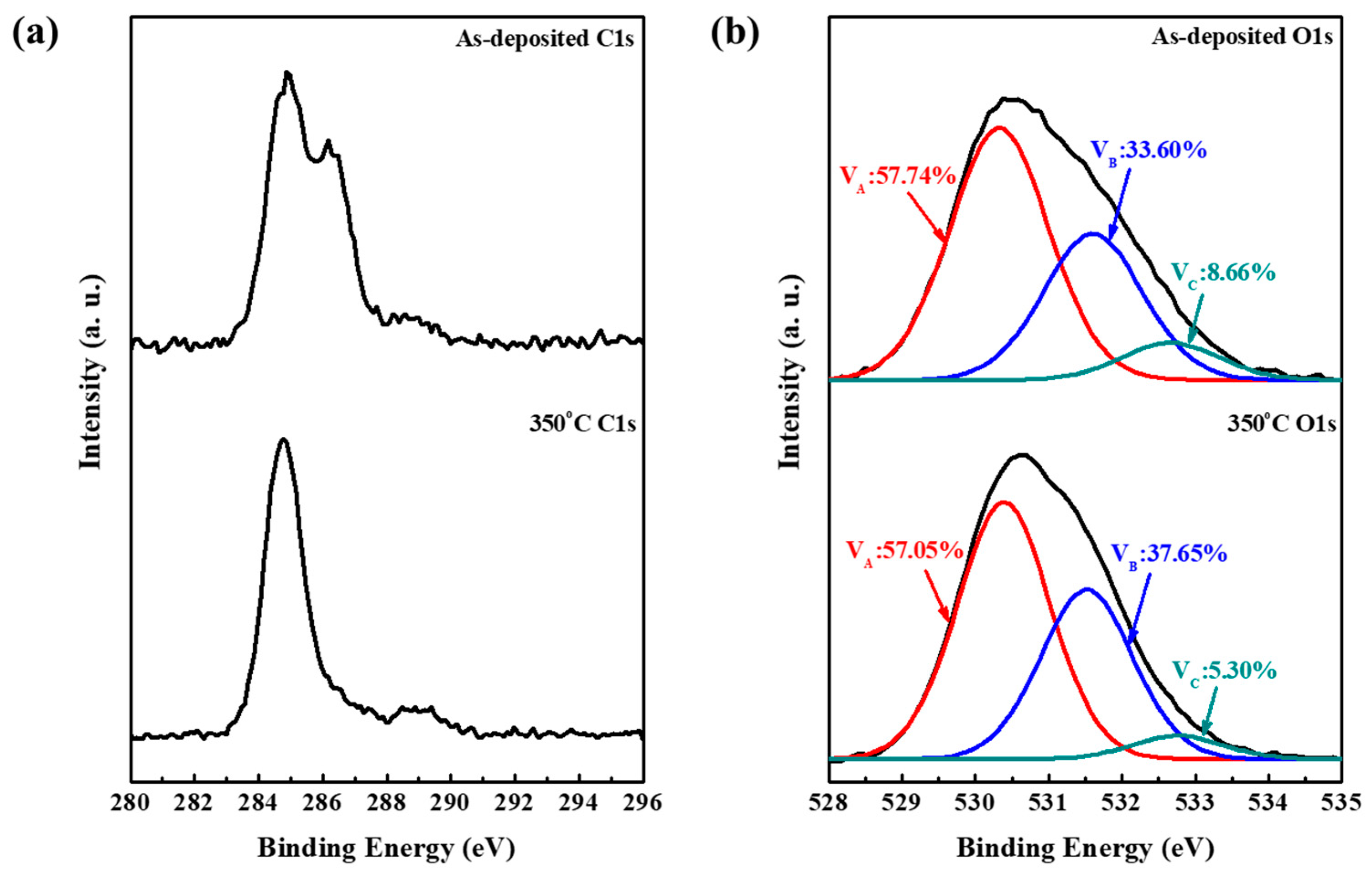
Currently, oxygen vacancies are closely related to the field-effect mobility and threshold voltage of metal-oxide-semiconductor devices, according to the equation:
[
20]. The XPS analysis of the channel region was implemented, as displayed in
Figure 4. All binding energies were corrected by referencing to the C1s peak (centered at 284.8 eV). From the C1s spectra in
Figure 4a, it clearly revealed that the photoresist was not thoroughly eliminated in the channel region of as-deposited devices. And the contamination was dramatically eliminated in the channel region after being annealed at 350 °C in air ambient. The O1s peak of a-STO channel layer could be de-convoluted into three principal sub-peaks via using a Gaussian-Lorentzian profile, which centered at 530.5 ± 0.3 eV (peak A), 531.8 ± 0.2 eV (peak B), and 532.7 ± 0.1 eV (peak C), respectively. The lowest binding energy located at 530.5 ± 0.3 eV was associated with oxygen-lattice bonds (Sn-O and Si-O) in a-STO compound system. The middle binding energy, centered at 531.8 ± 0.2 eV, was assigned to the oxygen vacancies. The highest binding energy positioned at 532.7 ± 0.1 eV was usually attributed to the presence of loosely bound oxygen on species, with a surface of the a-STO film such as -CO
3, -OH or adsorbed O
2. After the unpassivated device was annealed at 350 °C, a distinct increased area proportion of V
B (B/(A + B + C)), from 33.60% to 37.64%, and an obvious decreased proportion of V
C (C/(A + B + C)), from 8.66% to 5.30%, were found. These results indicated that the pre-annealing could not only effectively remove the contamination but also facilitate the increase of carrier concentration.
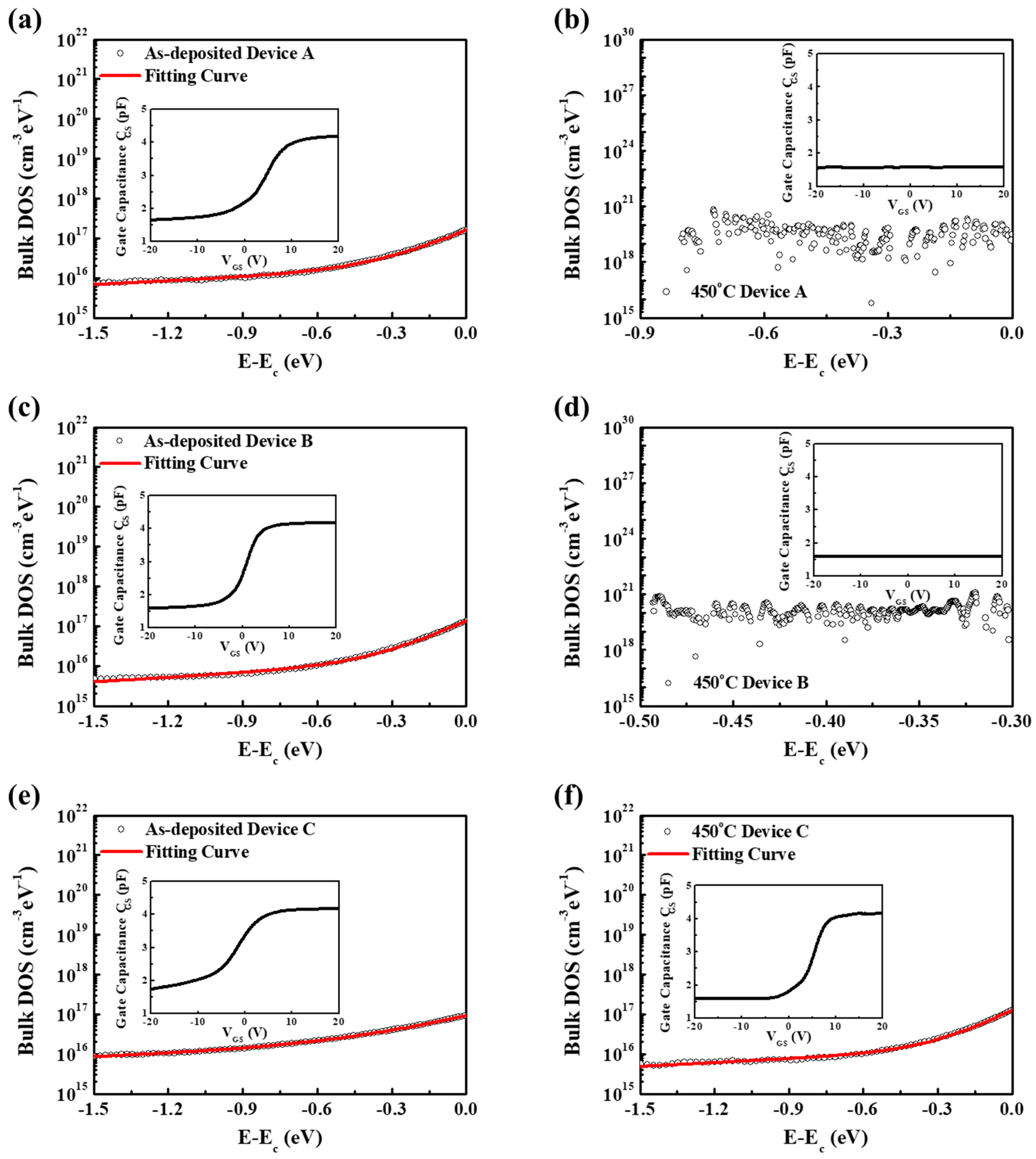
In AMOS devices, the sub-gap density of states (DOS) is an important parameter closely related to the mobility, operation voltage, and subthreshold swing of TFTs. To gain an insight into the reason for a series of changes in device performance, the acceptor-like DOS of a-STO TFTs was extracted by a low-frequency capacitance-voltage (C-V) characteristic [
21]. The results of C-V characteristics and DOS of a-STO TFTs were exhibited in
Figure 5. The DOS of devices might be divided into two parts: deep states and tail states, which could be approximately represented by the superposition of the exponential tail states and exponential deep states:
where N
DA, N
TA, E
DA, E
TA, E, and E
c is the density of deep states, the density of tail states, the energy of deep states, the energy of tail states, the state energy, and the conduction band minimum, respectively. The N
DA/N
TA is extracted by extrapolating the deep/tail states to E = E
c, while E
DA/E
TA is extracted from the slope of log(N
t) versus (E − E
c) for the deep/tail states. The fitting results of DOS of a-STO TFTs were shown in
Table 2. The density of deep/tail states (2.02 × 10
18/4.61 × 10
20 cm
−3 eV
−1) of Device A annealed at 350 °C in air ambient was obtained (See
Figure S2). The passivation layer could effectively degrade DOS of device. Quantities of defects were generated in the Device A and Device B after they were annealed at 450 °C in argon ambient, which led to the deterioration of device performance. For Device C, the density of deep states decreased from 1.97 × 10
16 cm
−3 eV
−1 to 1.44 × 10
16 cm
−3 eV
−1 after thermal post-annealing, while the density of tail states increased from 0.73 × 10
17 cm
−3 eV
−1 to 1.13 × 10
17 cm
−3 eV
−1. The reason for the decrease of density of deep states was attributed to the reduction of excess oxygen in a-STO film [
22]. Due to the existence of nonstoichiometric SiO
x, excess oxygen in the bulk a-STO film was attracted to the SiO
x/a-STO interface after post-annealing (See
Figure S3). The increase of density of tail states might be associated with the elimination of hydrogen (
) because the
ion can capture electrons to form stable
.
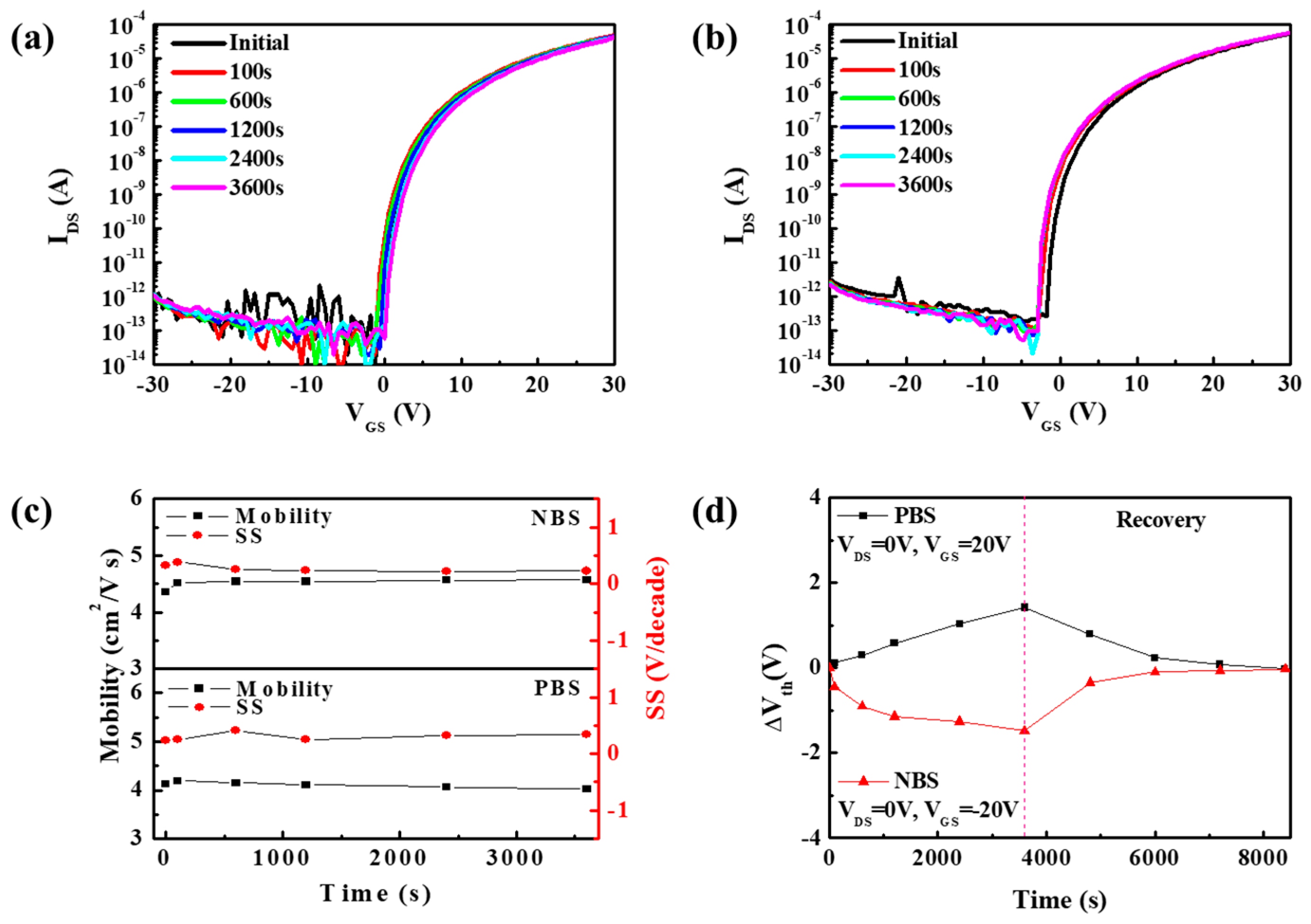
The electrical stability is a very important parameter for AMOS-TFTs backplane in display. The investigation of PBS and NBS electrical instabilities of Device C was performed, as illustrated in
Figure 6a,b. The threshold voltage shift (ΔV
th) under stress phase was 1.42 V (PBS) and −1.48 V (NBS), respectively. After both bias stresses were applied, the V
th of device could spontaneously recover to its initial state after a period of relaxation of 4800 s. It is well known that there are two major mechanisms causing V
th instability: (1) defect creation in the channel and (2) charge trapping in the gate insulator and/or at the channel/insulator interface [
23]. The negligible variation of mobility and SS (
Figure 6c) and the recovery of V
th without any annealing procedure (
Figure 6d) after relaxation indicated that the charge trapping in the bulk dielectric layers or interface was the dominant mechanism responsible for V
th instability. Thus, the charge trapping model could be reflected in the stress time dependence of ΔV
th, well-fitted with the stretched-exponential equation [
24]:
where ΔV
th0 is the ΔV
th at infinite time, t is the stress time, τ is the characteristic time constant for trapping, and β is the stretched-exponential exponent, respectively.
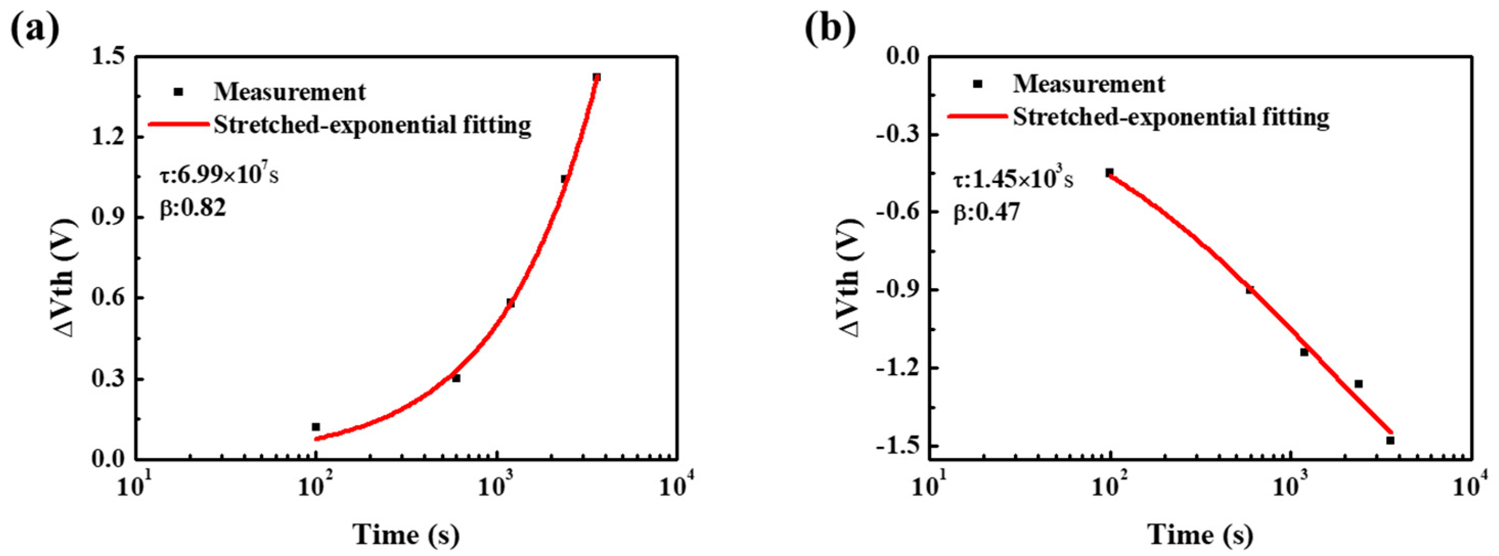
Figure 7 shows the fitting curves of time dependence of ΔV
th under PBS and NBS conditions. The characteristic time constant τ was 6.99 × 10
7 s (PBS) and 1.45 × 10
3 s (NBS) while stretched-exponential exponent β was 0.82 (PBS) and 0.47 (NBS), respectively.

 ,
, 


