Screen Printed Pb3O4 Films and Their Application to Photoresponsive and Photoelectrochemical Devices


Abstract
:1. Introduction
2. Experimental
2.1. Materials
2.2. Methods
2.2.1. Pb3O4 Powder Synthesis and Paste Preparation
2.2.2. Screen Printing of Pb3O4 Films
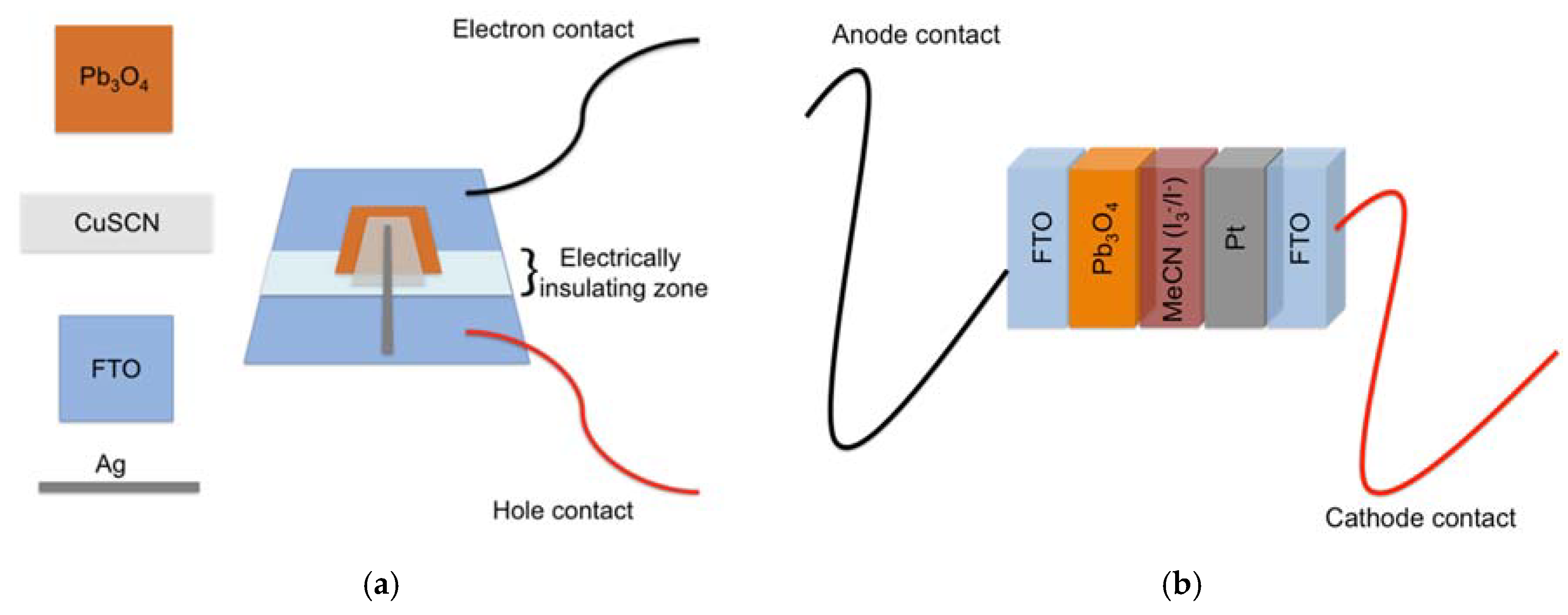
2.2.3. Photoresponsive Devices and Photoelectrochemical Cells Preparation
2.3. Structural and Morphological Characterization
2.3.1. XRD
2.3.2. UV-Vis Spectroscopy
2.3.3. FESEM
2.4. Device Test
2.4.1. Photoresponsive Device Test
I-V Curves and Response of the Device
2.4.2. Photoelectrochemical Cell Test
J-V Curves
Electrochemical Impedance Spectra
Incident Photon to Current Conversion Efficiency
3. Results and Discussion
3.1. XRD
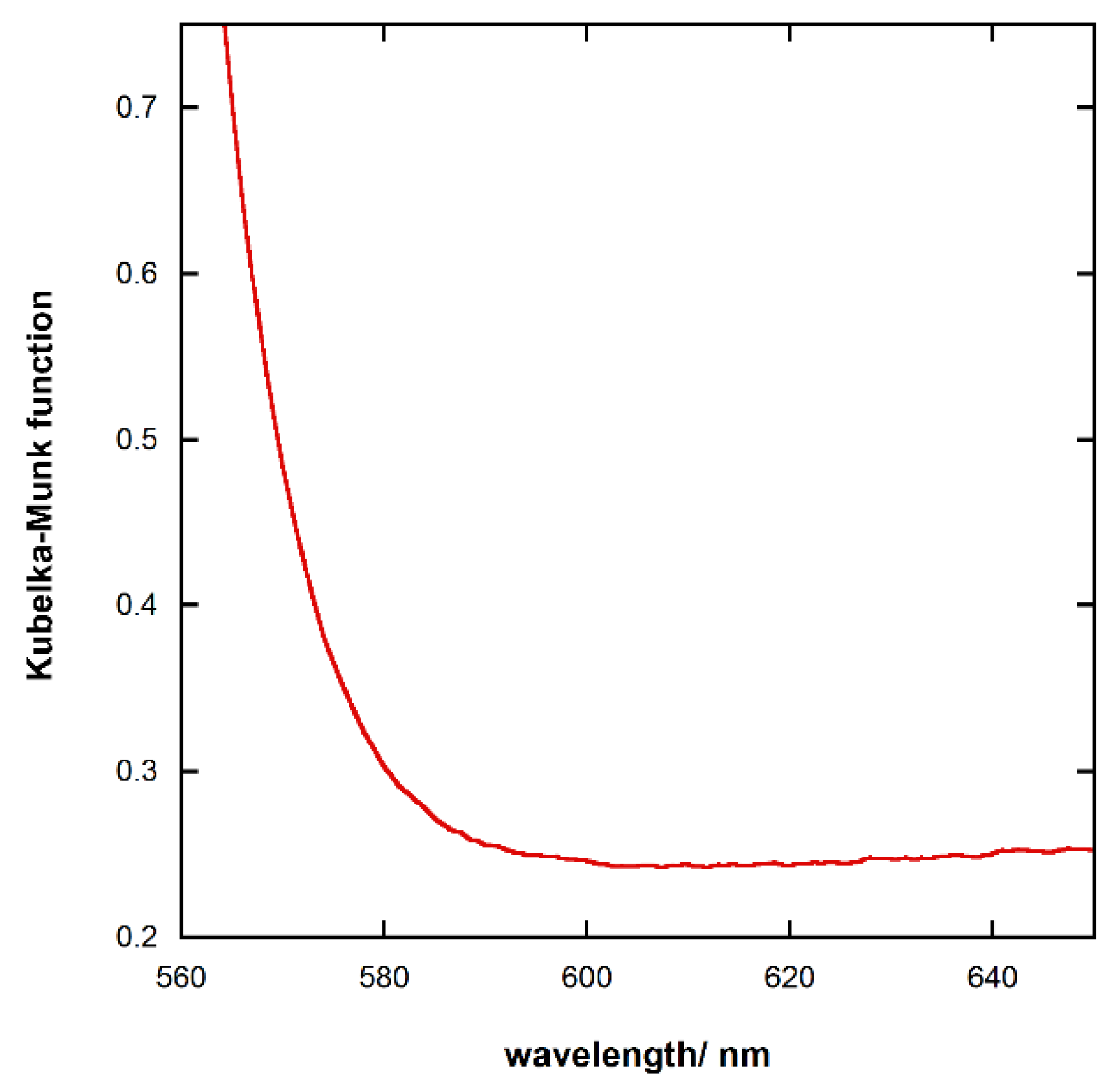
3.2. UV-Vis Spectroscopy
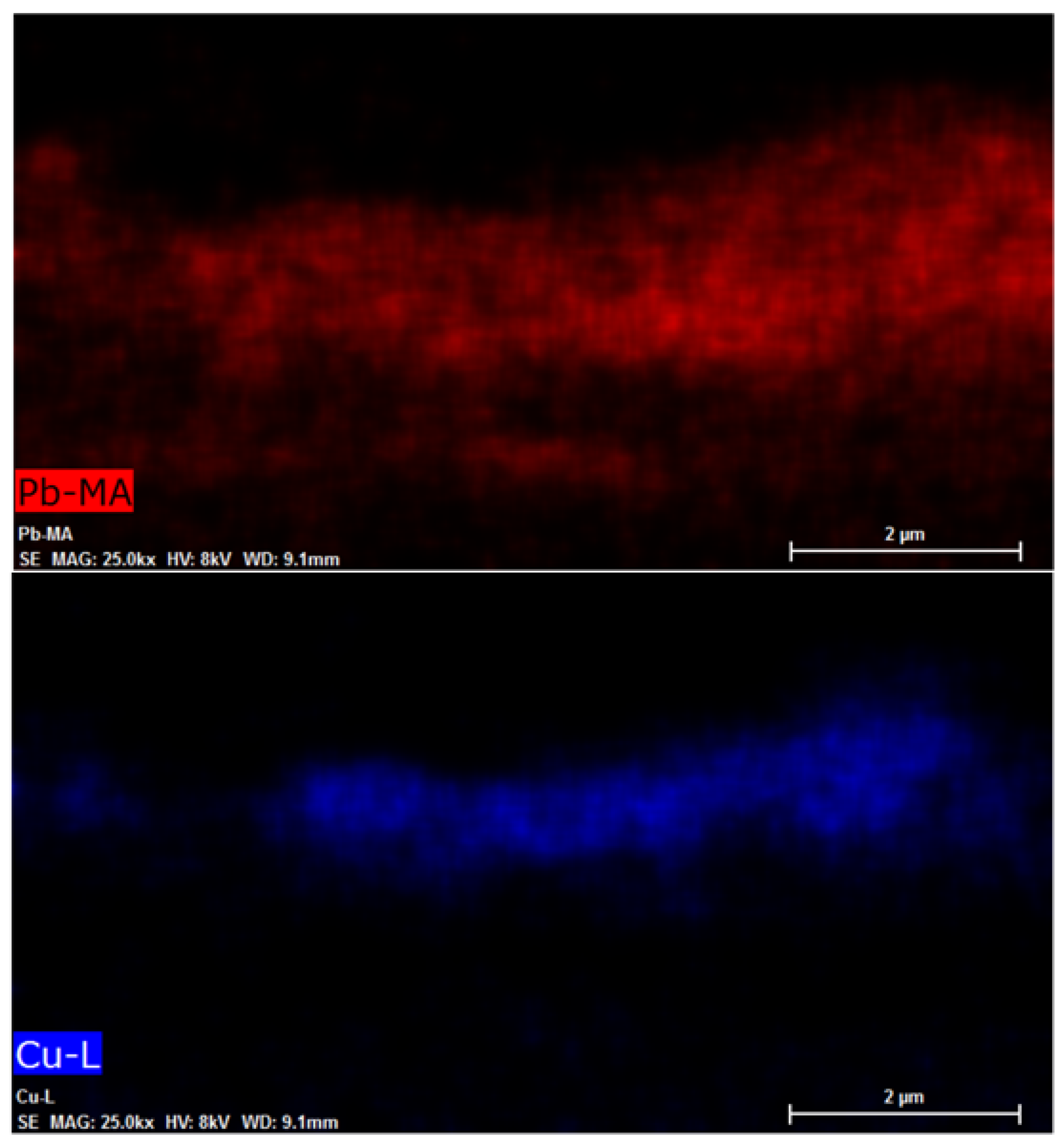
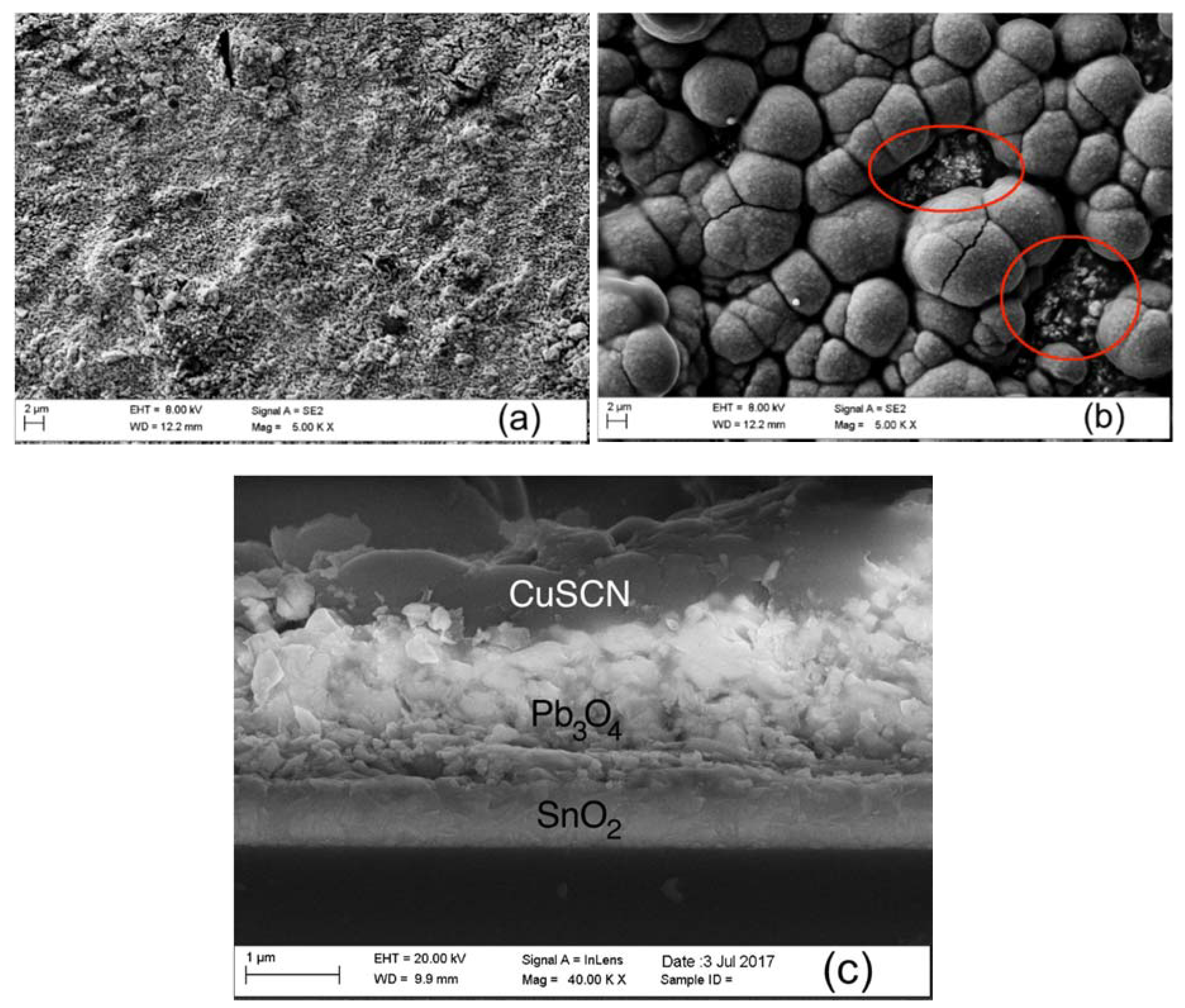
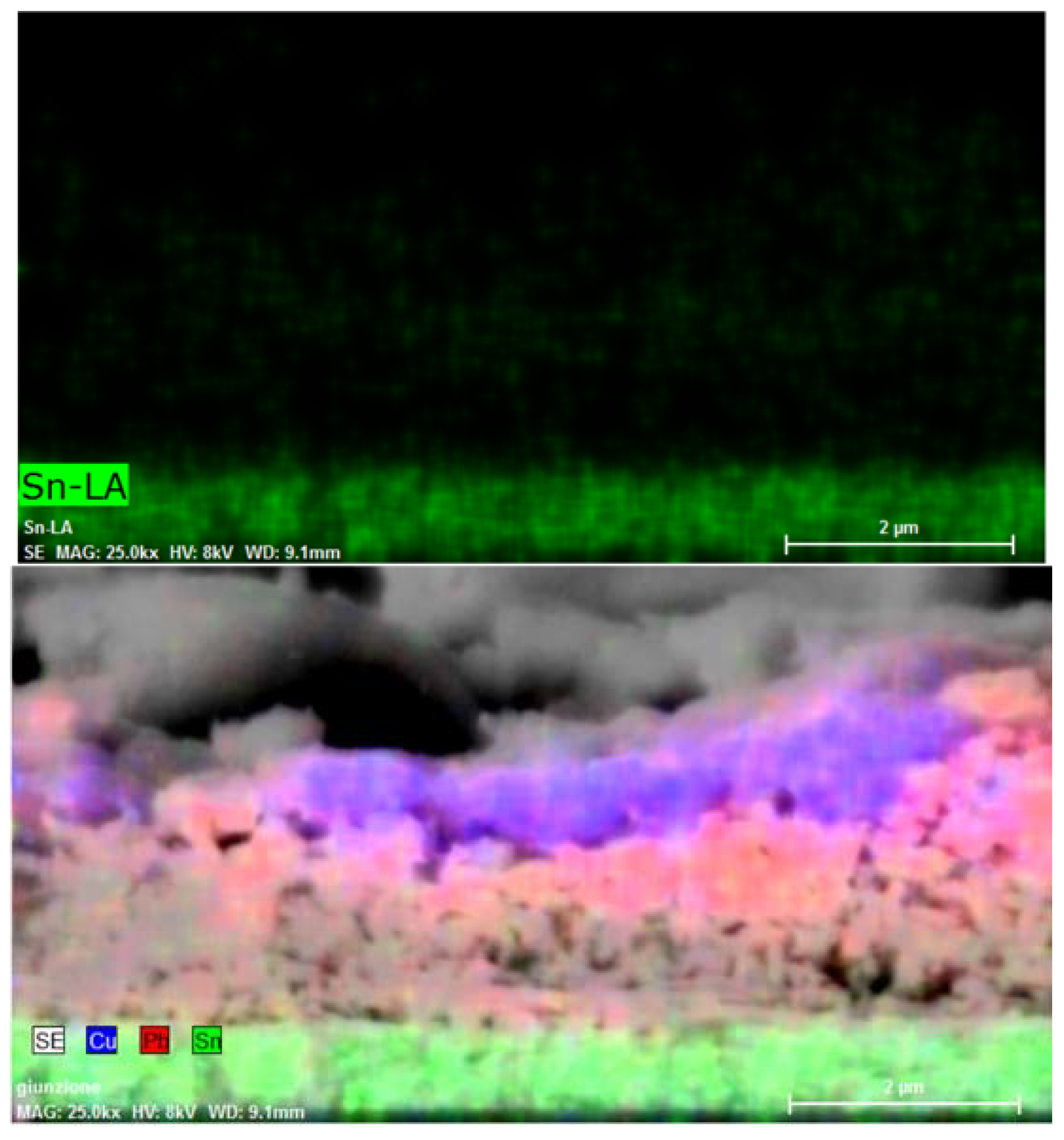
3.3. FESEM
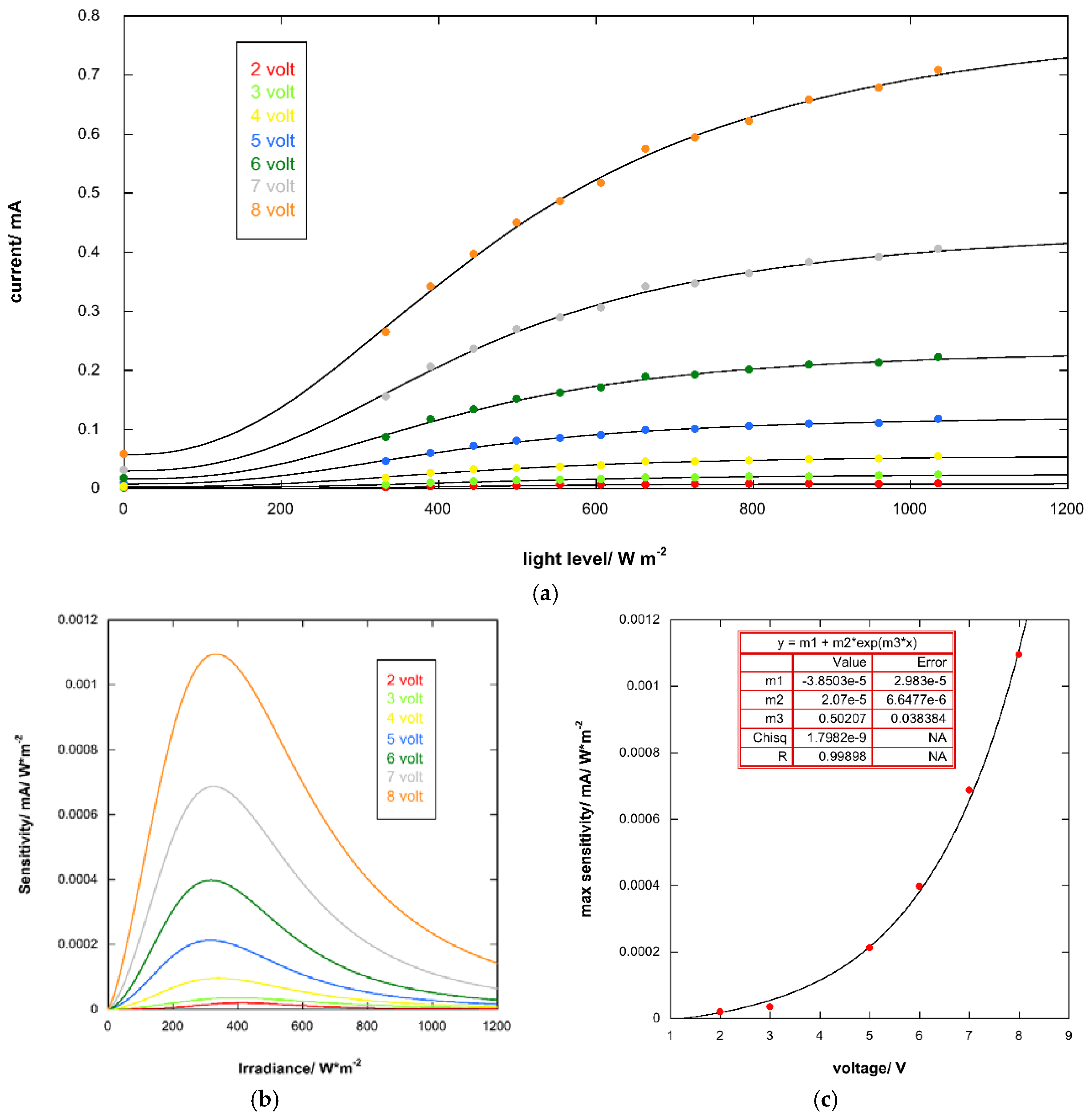
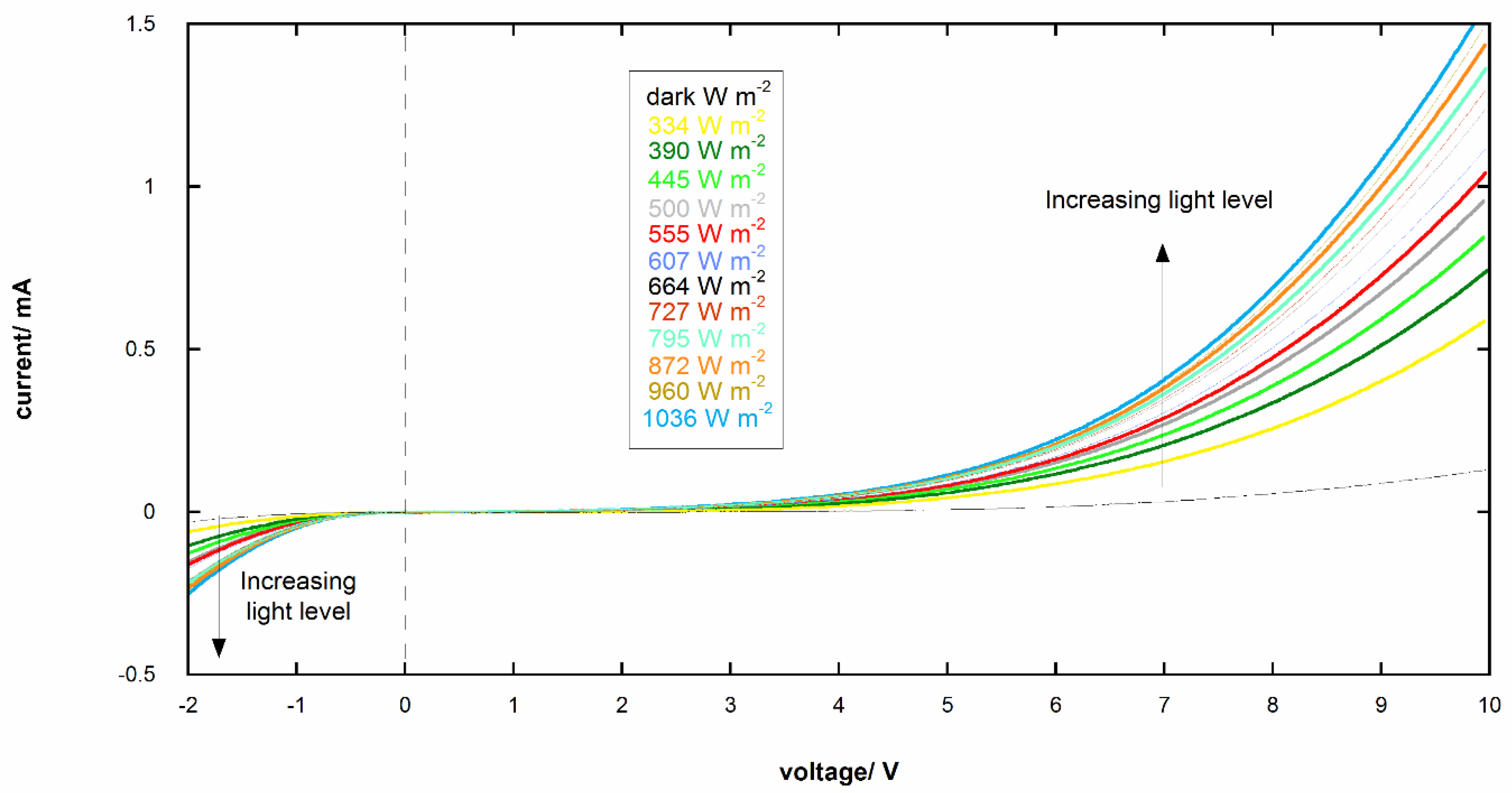
3.4. I-V Curves of Photoresponsive Device
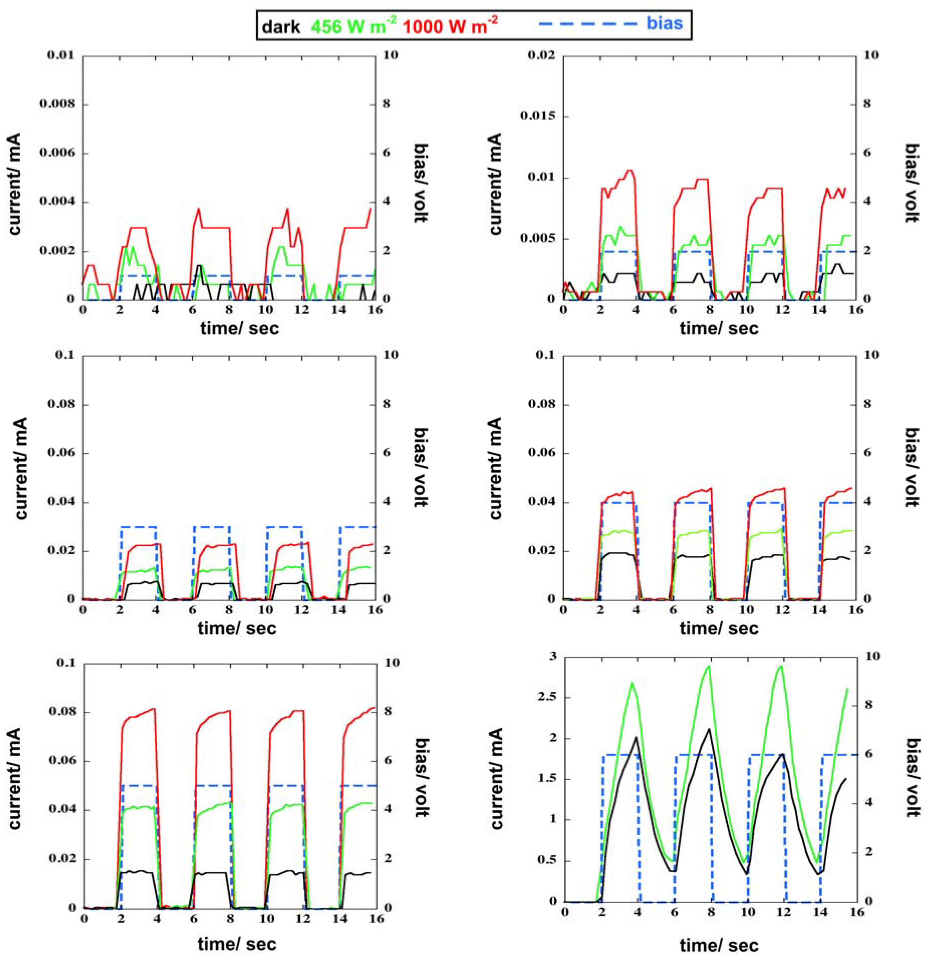
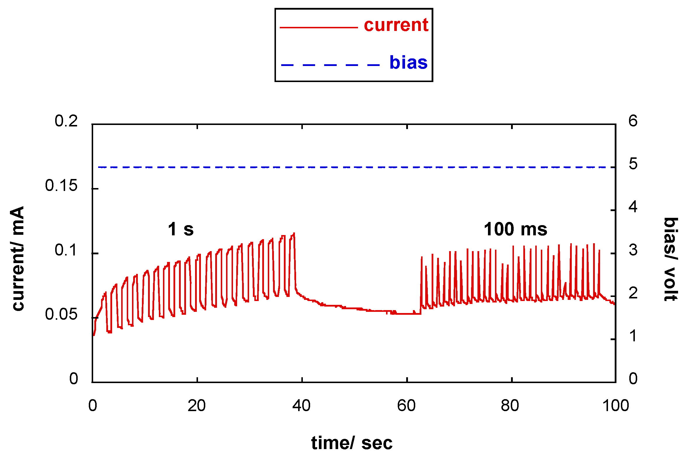
3.5. Response of the Photoresponsive Device
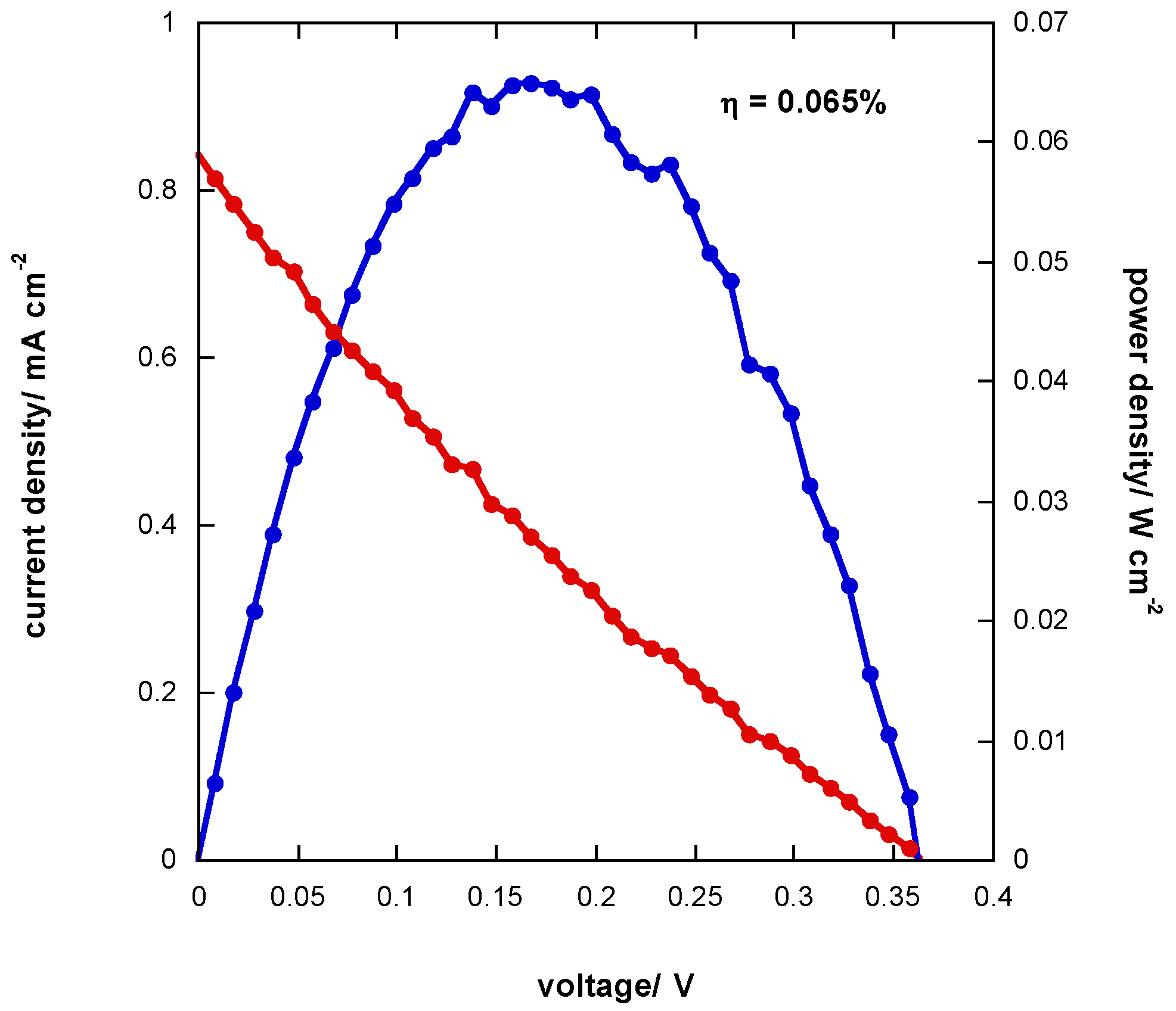
3.6. J-V Curve of Photoelectrochemical Cell
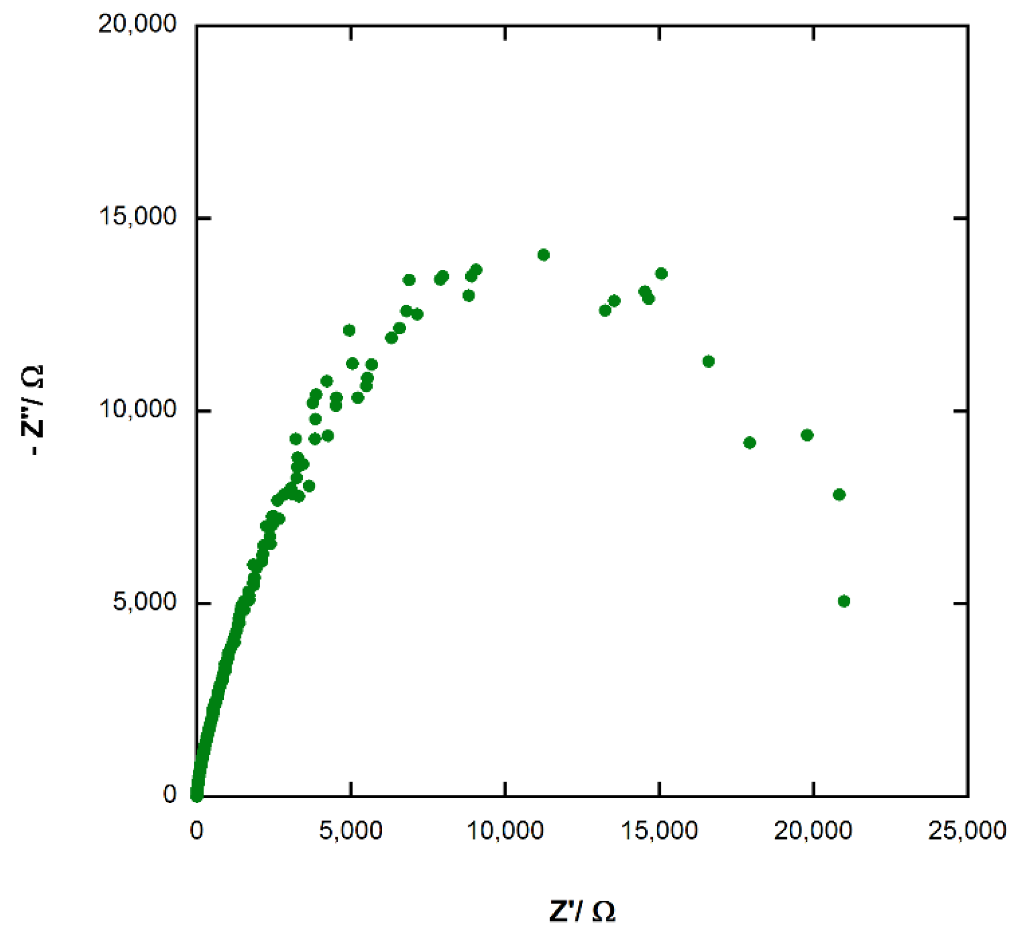
3.7. Electrochemical Impedance Spectroscopy (EIS) of Photoelectrochemical Cel
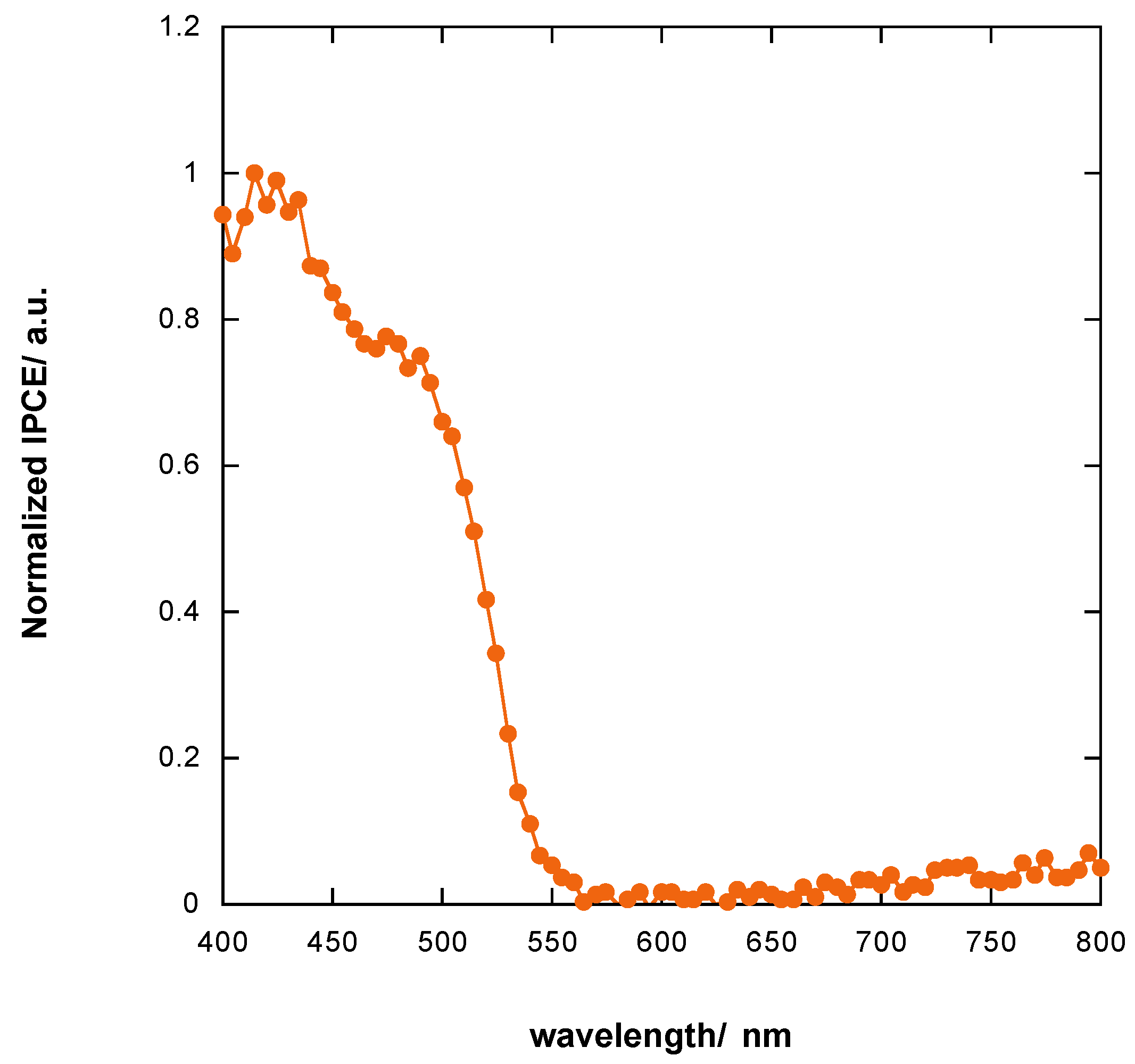
3.8. Incident Photon to Current Efficiency (IPCE) of Photoelectrochemical Cell
4. Conclusions
Author Contributions
Funding
Acknowledgments
Conflicts of Interest
References
- Thomson, D. The Materials and Techniques of Medieval Painting; Courier Corporation: Chicago, IL, USA, 1956. [Google Scholar]
- Sharon, M.; Kumar, S.; Sathe, N.P.; Jawalekar, S.R. Study of a Rechargeable Solar Battery with n-Pb3O4 Electrodes. Sol. Cells 1984, 12, 353–361. [Google Scholar] [CrossRef]
- Zhou, Y.; Long, J.; Gu, Q.; Lin, H.; Lin, H.; Wang, X. Photoinduced Reactions between Pb3O4 and Organic Dyes in Aqueous Solution under Visible Light. Inorg. Chem. 2012, 51, 12594–12596. [Google Scholar] [CrossRef] [PubMed]
- Sharon, M.; Kumar, S.; Jawalekar, S.R. Characterization of Pb3O4 films by electrochemical techniques. Bull. Mater. Sci. 1986, 8, 415–418. [Google Scholar] [CrossRef]
- Cao, M.; Hu, C.; Peng, G.; Qi, Y.; Wang, E. Selected-Control Synthesis of PbO2 and Pb3O4 Single-Crystalline Nanorods. J. Am. Chem. Soc. 2003, 125, 4982–4983. [Google Scholar] [CrossRef] [PubMed]
- Kumar, S.; Sharon, M. Preparation of a Thin Film of Pb3O4 by Thermal Treatment of PbO2. Thin Solid Film 1991, 195, 273–278. [Google Scholar] [CrossRef]
- Arami, H.; Mazloumi, M.; Khalifehzadeh, R.; Sadrnezhaad, S.K. Surfactant free hydrothermal formation of Pb3O4 nanorods. J. Alloys Compd. 2008, 466, 323–325. [Google Scholar] [CrossRef]
- Poll, C.G.; Payne, D.J. Electrochemical Synthesis of PbO2, Pb3O4 and PbO Films on a Transparent Conduction Substrate. Electrochim. Acta 2015, 156, 283–288. [Google Scholar] [CrossRef]
- Pattanasattayavong, P.; Promarak, V.; Anthopoulos, T.D. Electronic Properties of Copper (I) Thiocyanate (CuSCN). Adv. Sci. News 2017, 3, 1600378. [Google Scholar] [CrossRef]
- O’Regan, B.; Schwartz, D.T. Efficient Photo-Hole Injection from Adsorbed Cyanine Dyes into Electrodeposited Copper(I) Thiocyanate Thin Films. Chem. Mater. 1995, 7, 1349–1354. [Google Scholar] [CrossRef]
- Ito, S.; Murakami, T.N.; Comte, P.; Liska, L.; Grätzel, C.; Nazeeruddin, M.K.; Grätzel, M. Fabrication of thin film dye sensitized solar cells with solar to electric power conversion efficiency over 10%. Thin Solid Film 2008, 516, 4613–4619. [Google Scholar] [CrossRef]
- Kumara, G.R.R.A.; Konn, A.; Senadeera, G.K.R.; Jayaweera, P.V.V.; De Silva, D.B.R.A.; Tennakone, K. Dye-sensitized solar cell with the hole collector p-CuSCN deposited from a solution in n-propyl sulphide. Sol. Energy Mater. Sol. Cells 2001, 69, 195–199. [Google Scholar] [CrossRef]
- Latini, A.; Aldibaja, F.K.; Cavallo, C.; Gozzi, D. Benzonitrile based electrolytes for best operation of dye sensitized solar cells. J. Power Sources 2014, 269, 308–316. [Google Scholar] [CrossRef]
- Latini, A.; Panetta, R.; Cavallo, C.; Gozzi, D.; Quaranta, S. A Comparison of the Performances of Different Mesoporous Titanias in Dye-Sensitized Solar Cells. J. Nanomater. 2015, 16, 149. [Google Scholar] [CrossRef]
- Cavallo, C.; Salleo, A.; Gozzi, D.; Di Pascasio, F.; Quaranta, S.; Panetta, R.; Latini, A. Solid Solutions of Rare Earth Cations in Mesoporous Anatase Beads and Their Performances in Dye-Sensitized Solar Cells. Sci. Rep. 2015, 5, 16785. [Google Scholar] [CrossRef] [PubMed] [Green Version]
- Tauc, J.; Grigorovici, R.; Vancu, A. Optical Properties and Electronic Structure of Amorphous Germanium. Phys. Status Solidi 1966, 15, 627–637. [Google Scholar] [CrossRef]
- International Centre. PDF-2 (Powder Diffraction File) Database on CDROM; International Centre for Diffraction Data: Newtown Square, PA, USA, 2001. [Google Scholar]
- Langford, J.I.; Wilson, A.J.C. Sherrer after Sixty Years: A Survey and Some New Results in the Determination of Crystallite Size. J. Appl. Cryst. 1978, 11, 102–113. [Google Scholar] [CrossRef]


| Band Gap | eV |
|---|---|
| Eg Absorption Onset | 2.138 ± 0.004 |
| Eg Allowed Direct | 2.221 ± 0.001 |
| Eg Forbidden Direct | 2.162 ± 0.002 |
| Eg Allowed Indirect | 2.134 ± 0.004 |
| Eg Forbidden Indirect | 2.087 ± 0.006 |
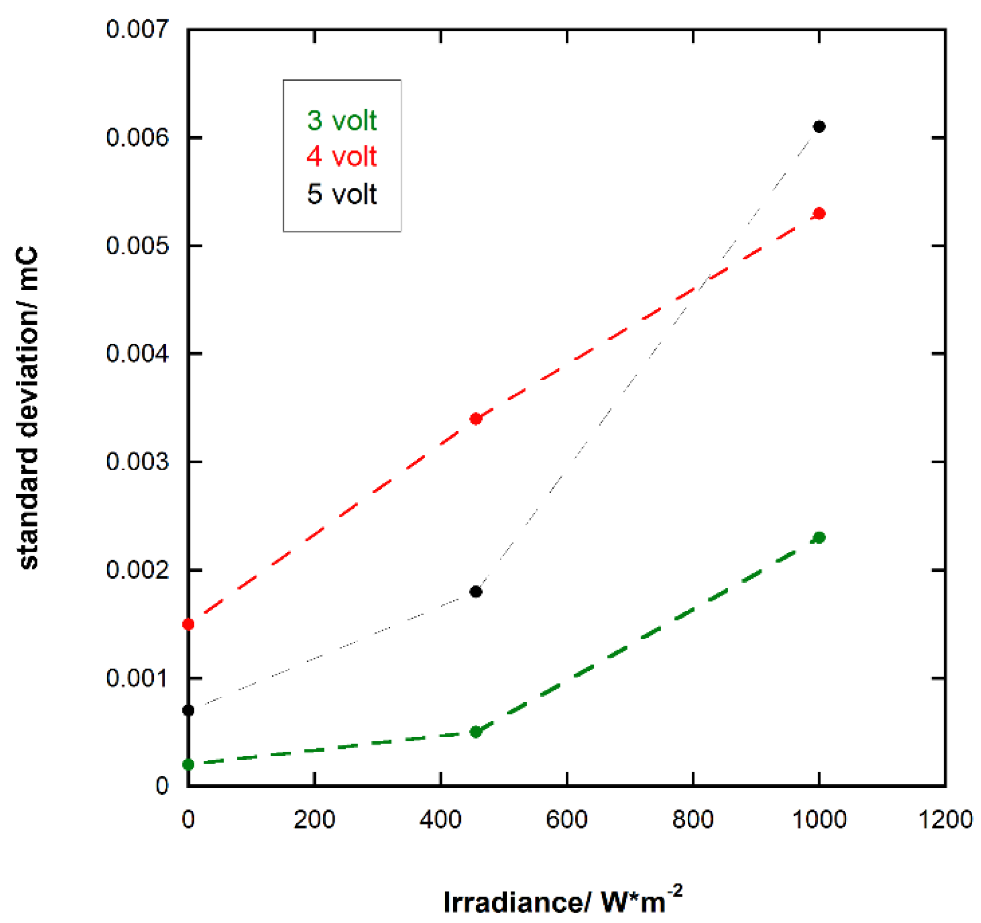
| Voltage/Volt | Irradiance/W m−2 | q1/mC | q2/mC | q3/mC | Average Value/mC | Standard Deviation/mC |
|---|---|---|---|---|---|---|
| 3 | dark | 0.0132 | 0.0135 | 0.0134 | 0.0134 | 0.0002 |
| 3 | 456 | 0.0252 | 0.0253 | 0.0261 | 0.0256 | 0.0005 |
| 3 | 1000 | 0.0440 | 0.0486 | 0.0464 | 0.0463 | 0.0023 |
| 4 | dark | 0.0393 | 0.0387 | 0.0364 | 0.0381 | 0.0015 |
| 4 | 456 | 0.0590 | 0.0526 | 0.0575 | 0.0564 | 0.0034 |
| 4 | 1000 | 0.0863 | 0.0953 | 0.0958 | 0.0925 | 0.0053 |
| 5 | dark | 0.0300 | 0.0287 | 0.0298 | 0.0295 | 0.0007 |
| 5 | 456 | 0.0841 | 0.0876 | 0.0857 | 0.0858 | 0.0018 |
| 5 | 1000 | 0.1685 | 0.1574 | 0.1586 | 0.1615 | 0.0061 |
© 2018 by the authors. Licensee MDPI, Basel, Switzerland. This article is an open access article distributed under the terms and conditions of the Creative Commons Attribution (CC BY) license (http://creativecommons.org/licenses/by/4.0/).
Share and Cite
Panetta, R.; Quaranta, S.; Latini, A. Screen Printed Pb3O4 Films and Their Application to Photoresponsive and Photoelectrochemical Devices. Materials 2018, 11, 1189. https://doi.org/10.3390/ma11071189
Panetta R, Quaranta S, Latini A. Screen Printed Pb3O4 Films and Their Application to Photoresponsive and Photoelectrochemical Devices. Materials. 2018; 11(7):1189. https://doi.org/10.3390/ma11071189
Chicago/Turabian StylePanetta, Riccardo, Simone Quaranta, and Alessandro Latini. 2018. "Screen Printed Pb3O4 Films and Their Application to Photoresponsive and Photoelectrochemical Devices" Materials 11, no. 7: 1189. https://doi.org/10.3390/ma11071189
APA StylePanetta, R., Quaranta, S., & Latini, A. (2018). Screen Printed Pb3O4 Films and Their Application to Photoresponsive and Photoelectrochemical Devices. Materials, 11(7), 1189. https://doi.org/10.3390/ma11071189