Article

Improved Optical and Electrochromic Properties of NiOx Films by Low-Temperature Spin-Coating Method Based on NiOx Nanoparticles

1
Siyuan Laboratory, Guangzhou Key Laboratory of Vacuum Coating Technologies and New Energy Materials, Guangdong Provincial Engineering Technology Research Center of Vacuum Coating Technologies and New Energy Materials, Department of Physics, Jinan University, Guangzhou 510632, China
2
Guangdong Tecsun Vacuum Technology Engineering Co. Ltd., Zhaoqing 526060, China
*
Authors to whom correspondence should be addressed.
Materials 2018, 11(5), 760; https://doi.org/10.3390/ma11050760
Submission received: 31 March 2018 / Revised: 22 April 2018 / Accepted: 7 May 2018 / Published: 9 May 2018
(This article belongs to the Section Thin Films and Interfaces)

Abstract

:
Solution approaches to NiOx films for electrochromic applications are problematic due to the need of an additional high-temperature annealing treatment step in inert gas. In this study, nanostructured NiOx powder with grain size of about 10.1 nm was synthesized for fabrication of NiOx films for electrochromic application. Non-toxic dispersants of isopropanol and deionized water were used and the whole process was carried out in air. The effects of the number of spin-coating layers, annealing temperature, and the volume ratios of isopropanol to deionized water were systematically investigated. Large transmittance change of 62.3% at 550 nm, high coloration efficiency (42.8 cm2/C), rapid switching time (coloring time is 4 s, bleaching time is 3 s), and good stability were achieved in the optimized NiOx film. The optimized process only required a low processing temperature of 150 °C in air with spin-coating three times and 1:2 volume ratio of isopropanol to deionized water. Finally, good cycle durability of up to 2000 cycles without obvious degradation was demonstrated by cyclic voltammetry tests in a LiClO4/propylene carbonate electrolyte. This study provides a simple and effective approach for fabrication of NiOx films at low temperature in air, which is attractive for further commercialization of electrochromic devices.

1. Introduction

According to statistics, building energy consumption accounts for 23–50% of total energy consumption [1]. Heat losses from windows and doors account for 20–30% of the whole building energy consumption [2]. Therefore, building energy conservation has become a hot topic. Electrochromism refers to reversible, persistent and visible change in transmittance or reflectance that is associated with an electrochemically induced oxidation-reduction reaction [3,4,5]. Electrochromic (EC) smart windows are a good choice to reduce the heat losses from windows due to their low energy consumption, lack of pollution and automatic adjustment of their optical properties [6].
Metal oxide material is a big family of inorganic EC materials that have been intensively studied [7,8,9,10,11,12,13]. They have excellent radiation resistances, high chemical stability, strong adhesions to substrates, and light weight over large areas [14]. Among all inorganic EC materials, NiO is one of the most important anodic coloring material due to its high optical modulation, fast responding time between coloring and bleaching processes, excellent durability, long-lasting memory, abundant raw materials and low-cost [10]. Complementary EC devices with NiO-based films as counter electrode layers have been extensively studied [11,12,13]. Chemical solution methods such as sol-gel methods [15,16,17,18,19], hydrothermal method [20,21,22] and chemical bath deposition (CBD) [23,24] have been widely used to fabricate NiO-based films for EC devices. Several ways are generally investigated to improve the optical and EC properties of NiO films. The first is to optimize the processing parameters such as thickness [12], annealing temperature [22], etc. Second is to improve the electrical properties by doping metal ions such as Al3+ [18], B3+ [25], Li+ [26], Co+ [23] in NiO films. Third is to make NiO-based films with multilayers [19,24,27,28]. Although the optimized optical and EC properties of NiO-based films are now acceptable in application, there is still one problem that hampers the reduction of fabrication cost and commercialization. High temperature annealing above 300 °C is required to improve the optical and EC properties of NiO-based films. In addition, protective gas or vacuum conditions are normally required in the fabrication process. Solving this problem becomes more important because of the increasing requirement of flexible EC devices, which must be fabricated on a substrate that cannot withstand temperature higher than 200 °C.
In this study, we showed the fabrication of NiOx films with superior optical and EC properties that required low-temperature annealing at 150 °C in air by the spin-coating method. We optimize the EC properties of NiOx films as a function of the number of spin-coating layers, annealing temperature, and the volume ratios of isopropanol (IPA) to deionized water (DI water) in the IPA-DI water-NiOx suspensions (NiOx inks). NiOx film with large transmittance change, high coloration efficiency, rapid switching time and good cyclic stability is obtained. We also discussed the microscopic differences between NiOx films to obtain a clear understanding of the differences in EC properties.

2. Materials and Methods

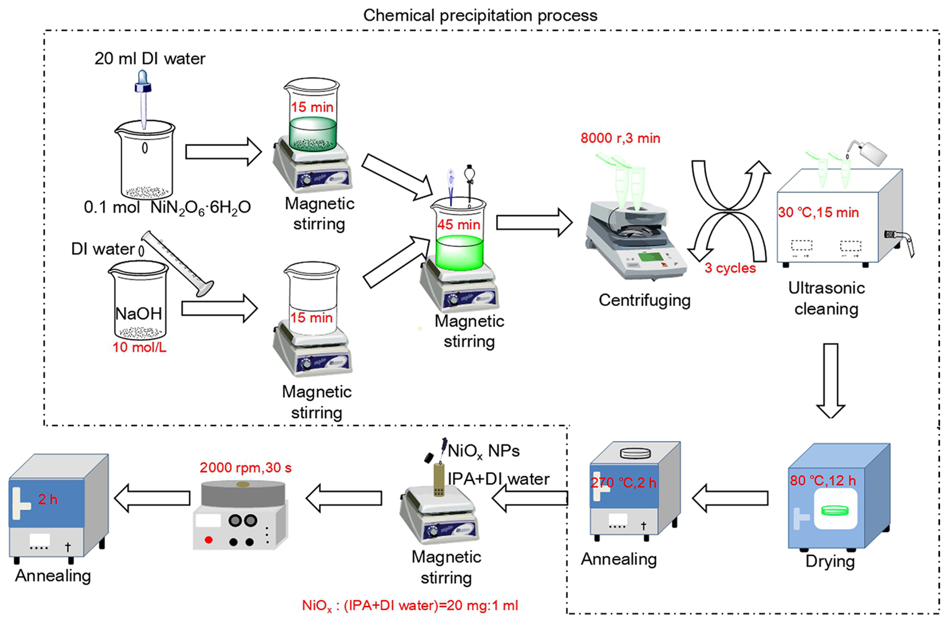
2.1. Fabrication of Samples

There are two methods to fabricate NiOx films with different numbers of layers. One is to spin multiple layers and anneal the films at the end. In this study, we choose this method to reduce the processing complexity. The other is to anneal the films whenever each layer is coated. Although this method is complex, it is reported to further improve the film quality, which will be studied later [29]. Figure 1 shows the fabrication flowchart of NiOx NPs and NiOx films. Firstly, we fabricated high-quality non-stoichiometric NiOx NPs similar to the facile chemical precipitation method of Fei Jiang and co-workers’ work [30]. 0.1 mol nickel nitrate hexahydrate (NiN2O6·6H2O, AR, 98%) was added into 20 mL DI water. After stirring, it formed a light green solution. Thenceforth, NaOH (AR, 98%) solution with a concentration of 10 mol/L was slowly added into the obtained solution until pH = 10. At this time, the green Ni(OH)2 colloidal precipitation was observed. The mixture was centrifuged and cleaned with an ultrasonic bath in DI water and circulated 3 times in turn. Then, the Ni(OH)2 precipitation was collected and dried at 80 °C for 12 h. Finally, this dried green product was annealed at 270 °C for 2 h in air to decompose into ultrafine dark-black NiOx NPs. The NiOx NPs can be stored for a long time for multiple uses. Reactions (1) and (2) illustrate the chemical reactions in this procedure of non-stoichiometric NiOx NPs [30]:
Ni ( NO ) 3 + NaOH Ni ( OH ) 2 + Na ( NO 3 ) 2
Ni ( OH ) 2 270   ° C NiO x + H 2 O
Secondly, we prepared NiOx inks. 20 mg of the above NiOx NPs were uniformly dispersed in 1 mL IPA-DI water mixture using magnetic stirring.
Thirdly, we fabricated NiOx samples by the spin-coating method. Conductive indium tin oxide (ITO, 10 Ω/sq) coated glasses were cleaned with acetone, ethanol, and DI water in an ultrasonic bath for 15 min in sequence before use. The above NiOx inks were spin-coated onto substrates with different numbers of coating layers (2000 rpm for 30 s each time). Finally, the NiOx samples were annealed for 2 h in air for the evaporation of the organic solvent.

2.2. Characterization

The morphology and structure of NiOx films and NiOx NPs were characterized by a field emission scanning electron microscope (FE-SEM, Zeiss Ultra 55, Carl Zeiss, Jena, Germany) and a XRD diffractometer (XRD, MiniFlex600, Cu Kα radiation, Rigaku, Tokyo, Japan). Electrochemical measurements of NiOx electrodes were performed by employing a three-electrode electrochemical workstation (Versa STAT 3, AMETEK, Oak Ridge, TN, USA) and carried out in a three-electrode system in 1 M KOH (AR, 90%) electrolyte: the as-prepared sample was used as working electrode, an Ag/AgCl electrode and a platinum wire were used as reference and counter electrodes, respectively. Before each electrochemical test, each sample was first circulated 12 times by applying square-wave-type voltages (±1.7 V, 60 s per cycle) until the responses become stabilized. The transmission spectra of NiOx films in fully colored and fully bleached states was measured over the wavelength range from 340 to 900 nm with a UV-vis spectrophotometer (Model UV-2550, Shimadzu, Tokyo, Japan). The transmittance of ITO-glasses in the 1 M KOH electrolyte was considered to be 100% transmittance and was used as the baseline.

3. Results

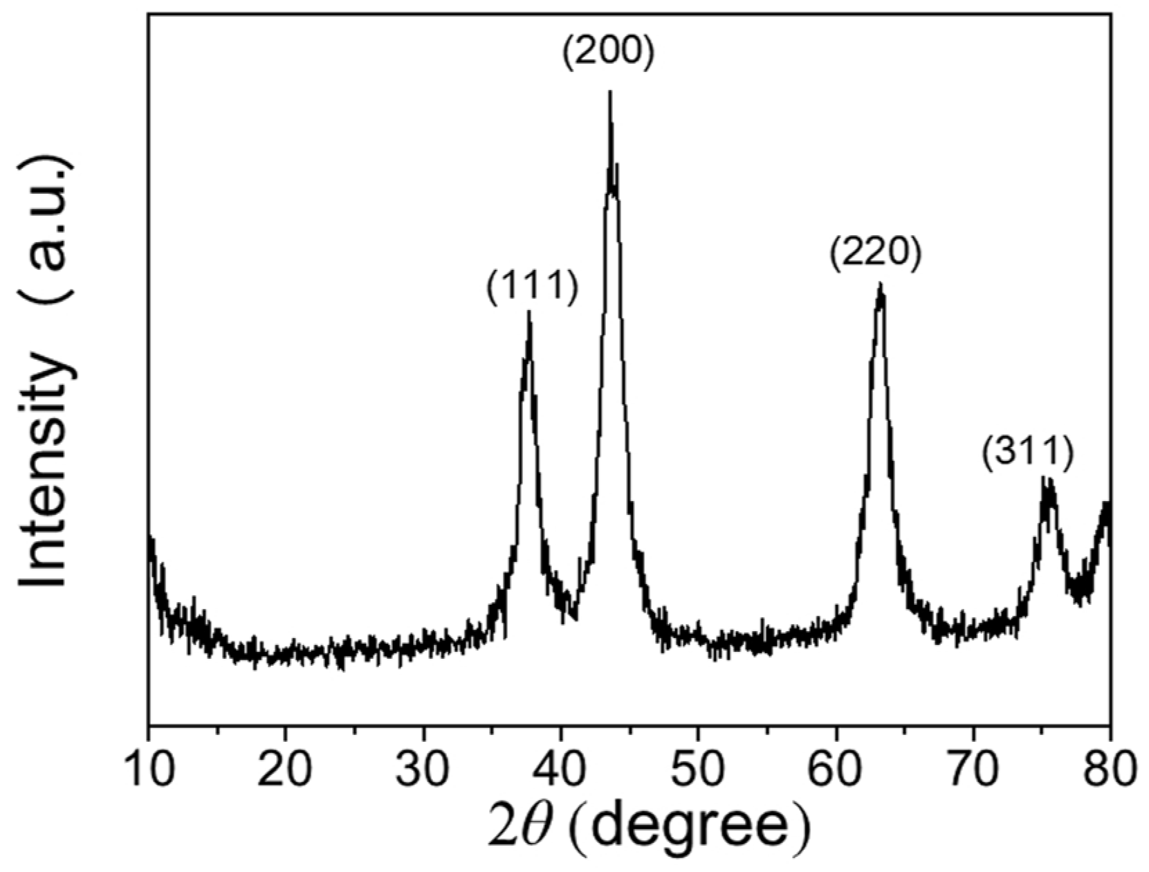
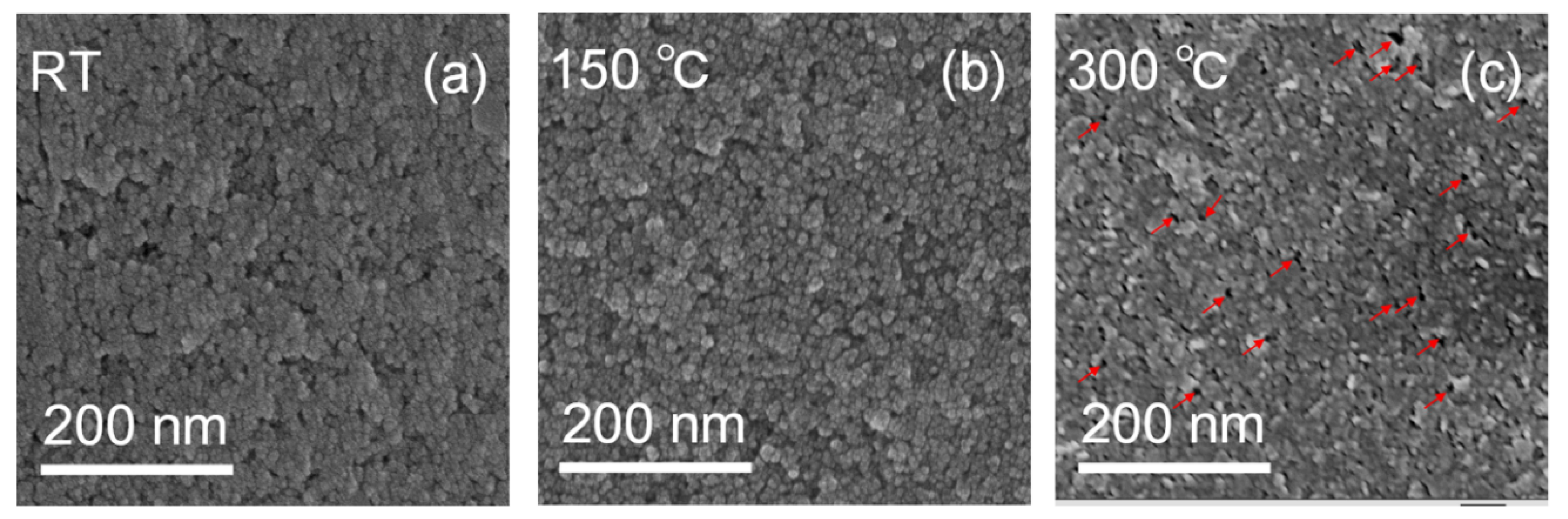
3.1. Microstructure Characteristics of the NiOx NPs

Figure 2 shows the XRD patterns of NiOx NPs. Four prominent characteristic diffraction peaks of NiOx cubic structure appears at 37.7°, 43.6°, 63.2° and 75.8°, belonging to the (111), (200), (220) and (311) planes (JCDPS No. 47-1049), the full width half maximum (FWHW) of the diffraction peaks are 0.805°, 0.878°, 0.978°, and 0.901°, respectively. No other peaks were observed. The crystallite size of the NiOx NPs can be estimated from the four XRD diffraction peaks by Debye-Scherrer formula [31]:
D = 0.89 λ B cos θ
where D is the size of crystallite, B is the FWHW. θ is the Bragg angle (degree) and λ (0.154056 nm) is the wavelength of the X-ray. The average NiOx crystallite size is estimated to be is 10.1 nm. The small grain size is favorable for ions to shorten diffusion pathway and increase the switching speed of NiOx films and increase the utilization efficiency of active materials. Such characteristics are favorable for a fast EC reaction [32,33].

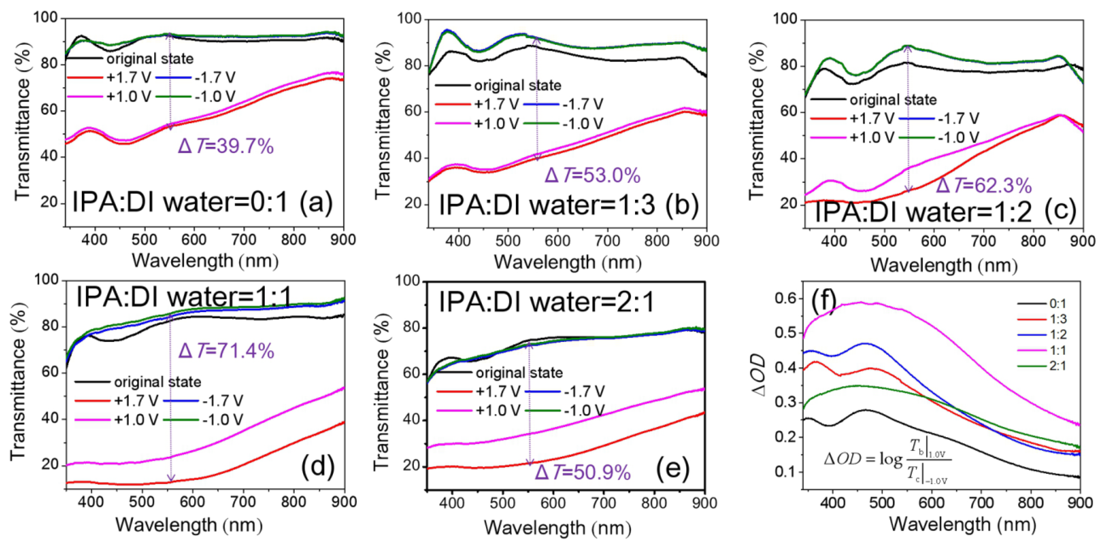
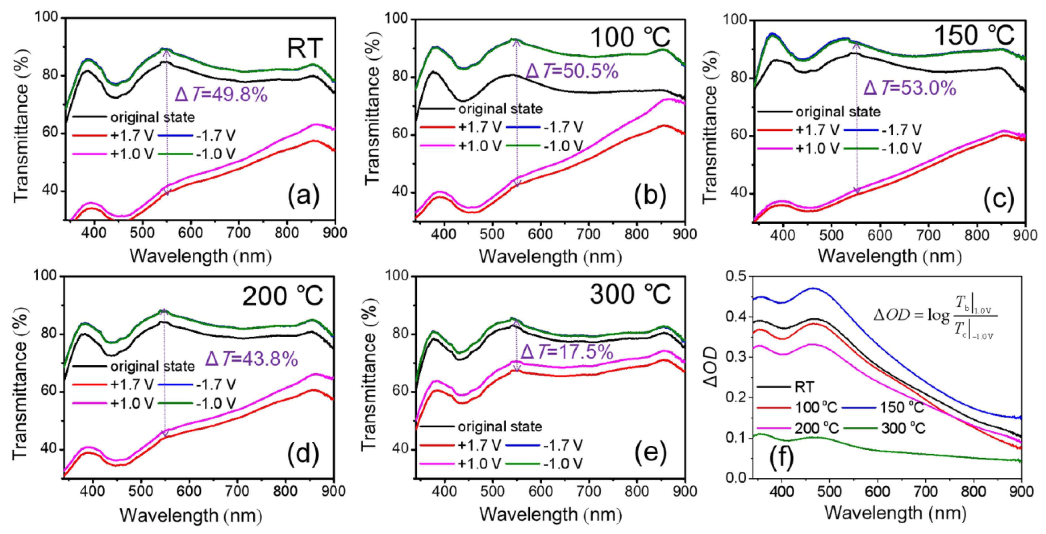
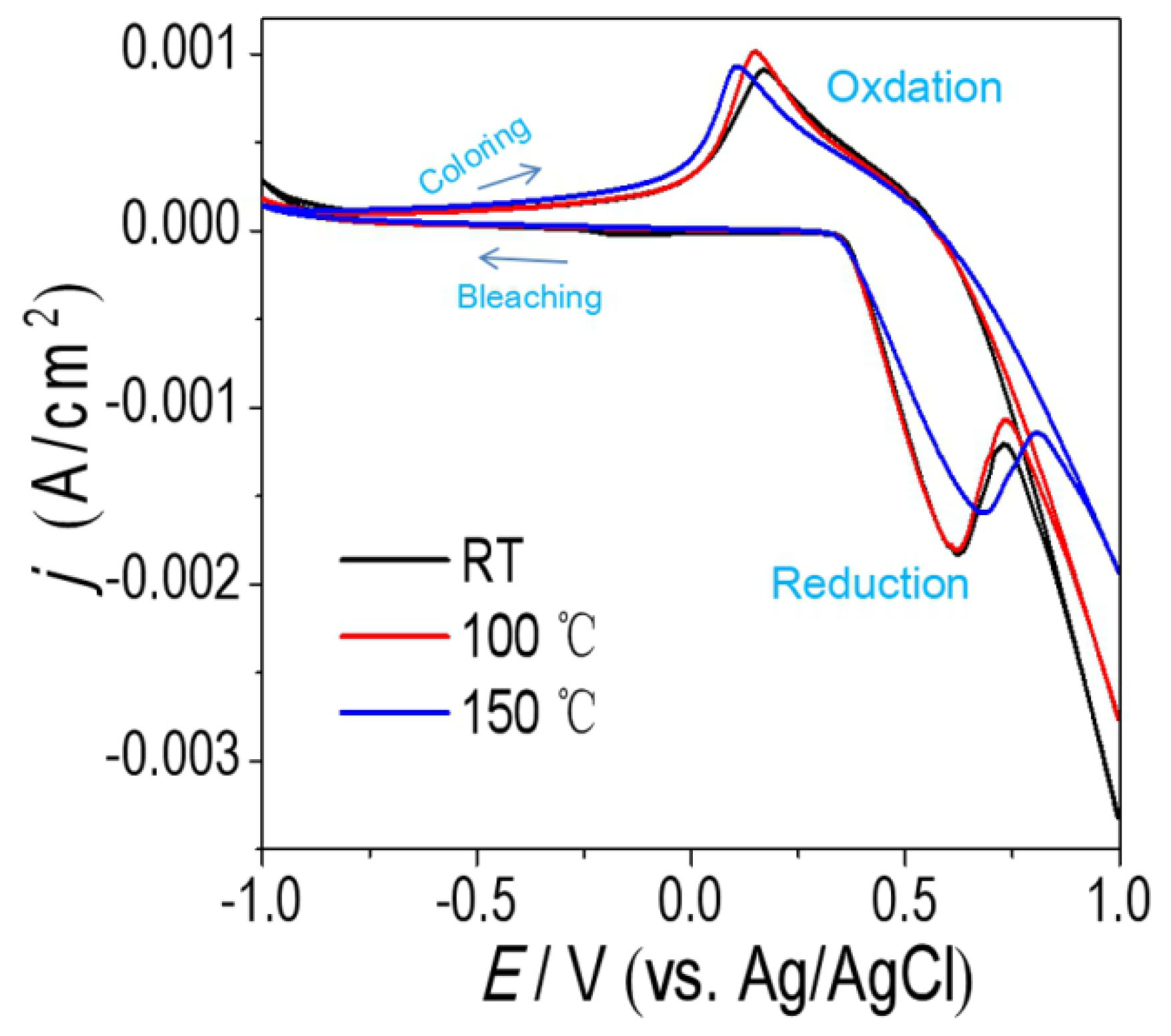
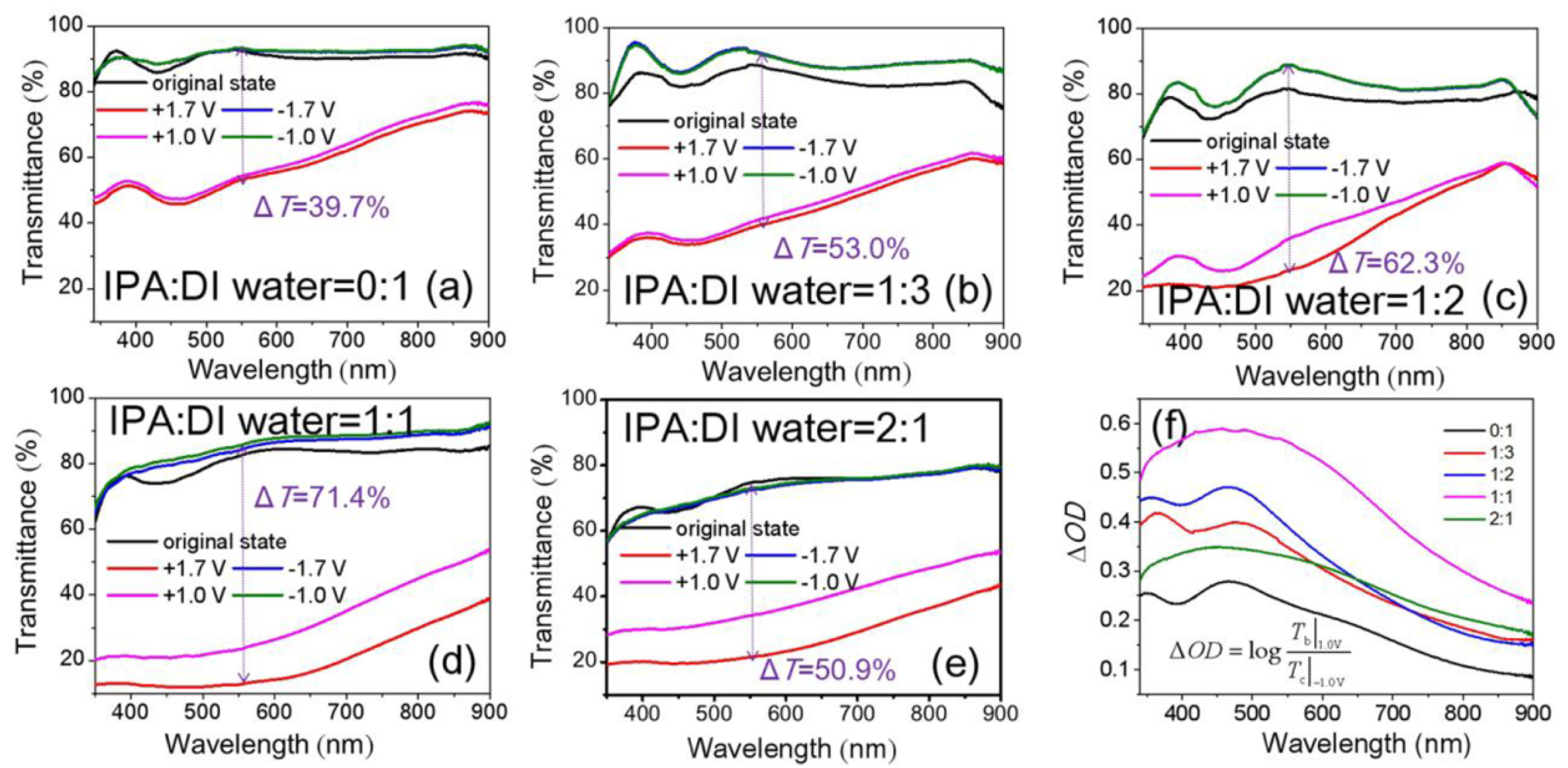
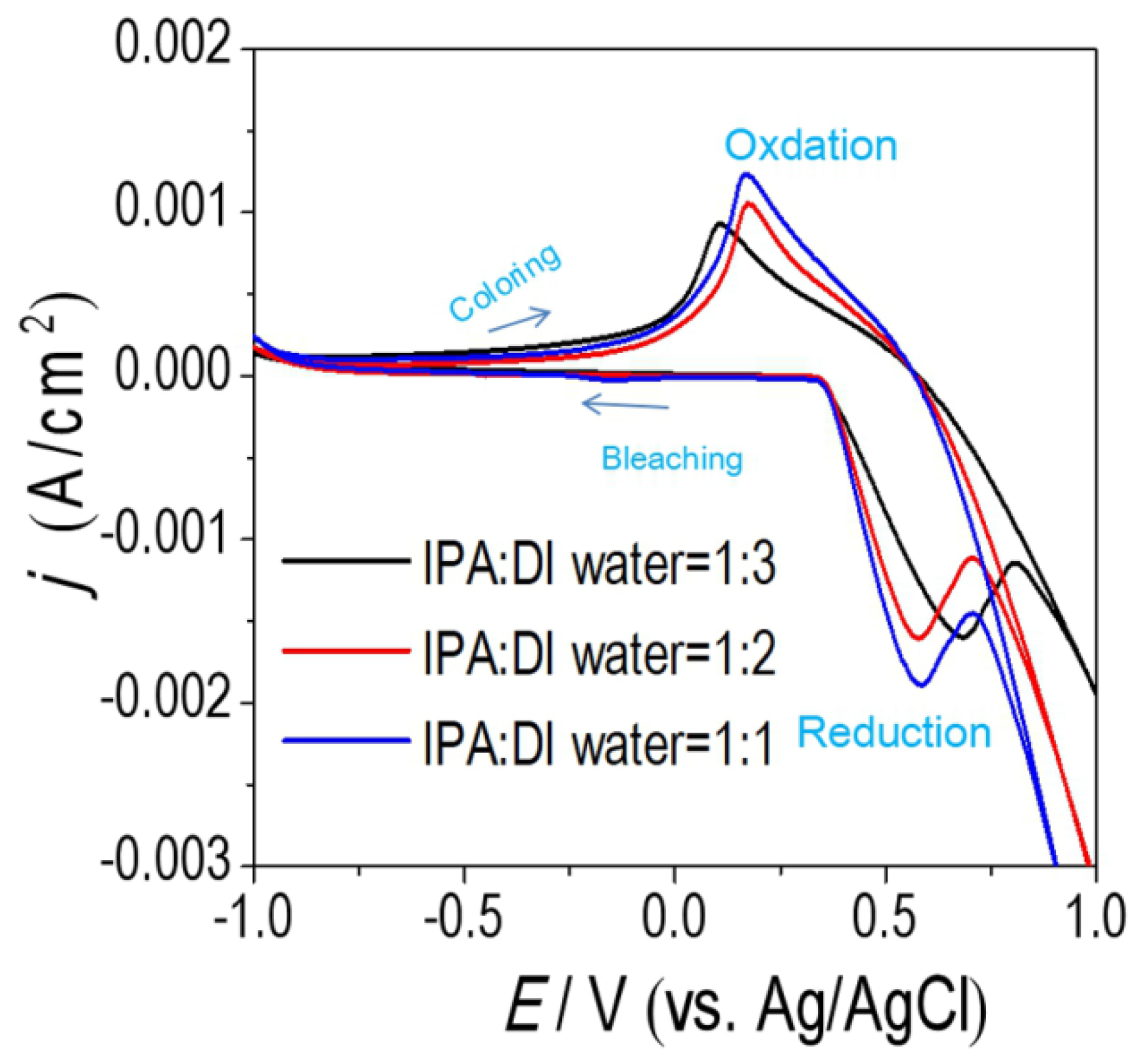
3.2. Optical and EC Properties of NiOx Films

The coloring processes of NiOx electrodes can be attributed to the following oxidation reactions [28]:
NiO + O H NiOOH + e
Or
NiO + H 2 O NiOOH + H + + e
The bleaching processes of the NiOx electrodes can be attributed to the following reduction reaction:
NiOOH + H + + e Ni ( OH ) 2
Or
NiOOH + H 2 O + e Ni ( OH ) 2 + OH
ΔT and switching time are the most important criteria indexes to evaluate optical and EC properties of materials. ΔT (TbTc) is the change of transmittance between the bleached states (Tb) and the colored states (Tc). The switching time is defined as the time required for a system to reach 90% of its full ΔT. Guofa Cai et al. [12] reported the optical and EC properties of inkjet-printed NiO films as a function of the number of printed layers. Sahu et al. [34] also reported the optical and EC properties of e-beam evaporated NiO films were affected with different thicknesses. Similarly, we studied the transmittance spectra of NiOx films at colored and bleached states as a function of the number of spin-coating layers. The results are shown in Figure 3a–d. Colored states of the NiOx films is obtained through applying positive voltages and bleached states by negative voltages. As the positive voltages increase from +1.0 V to +1.7 V, the transmittance of the colored states obviously decreases. However, the changes of the transmittance of the bleached states is not obvious when the negative voltage increases from −1.0 V to −1.7 V. The ΔT exhibits the best value of 50.5% at 550 nm varying from 93.0% to 42.5% between the bleached state (−1.7 V) and the colored state (+1.7 V). For the NiOx films after spin-coating three times, the ΔT gradually becomes lower. The change in optical density (ΔOD) is defined as [5]
Δ O D ( λ ) = log T b ( λ ) T c ( λ )
ΔOD represents the contrast between colored states and bleached states and it is presented in Figure 3e. Under the first spin-coating, the NiOx NPs partially cover the surface of ITO-glass, the ΔOD is small. Under the third spin-coatings, the surface is gradually filled, forming a complete layer, which shows the best ΔOD. Further increase in numbers of spin-coatings increases the thicknesses of the NiOx films. Because NiO and NiOH are semiconductors with extra-high resistances, the superfluous NiOx NPs do not contact with electroconductive ITO layer and are less active in electrochemical processes. Figure 3f shows the changes in transmittance at 550 nm of the NiOx film after spin-coating three times for applied square-wave-type voltages (±1.0 V, 60 s per cycle). It is calculated that the switching time is 3 s for the coloring process and 2 s for the bleaching process. The fast switching speed of the NiOx film is attributed to the short diffusion pathways in the NiOx NPs, which facilitates charge, transport [32,33].
Chen et al. [22] and Gamze Atak et al. [35] reported that annealing temperature is also an important parameter affecting the optical and EC properties of NiO-based films. Similarly, we studied the transmittance spectra of NiOx films by spin-coating three times as a function of the annealing temperature for 2 h in air after spin-coating. Figure 4a–e shows the transmittance spectra of NiOx films at colored and bleached states as a function of annealing temperature. As annealing temperature is 100–150 °C, the transmittance of the bleached states can be improved to over 90.0%. The ΔT of NiOx films annealed at room temperature (RT), 100 °C, 150 °C, 200 °C and 300 °C are 49.8%, 50.5%, 53.0%, 43.8% and 17.5% respectively between bleached states (−1.7 V) and colored states (+1.7 V). The ΔOD of the NiOx film annealed at 150 °C is the highest ΔOD compared to the others (Figure 4f). These differences of annealing effects can be explained by the changes of SEM morphology in Figure 5. If the NiOx film was not annealed, it can be seen that the NiOx NPs was not obvious because of the presence of residuary dispersants and organic binders (Figure 5a). Uniform and obvious NiOx NPs were observed after annealing at 150 °C as shown in Figure 5b. This was because the evaporation of the residuary dispersants and the decomposition of the organic binder led to an active electrochemical reaction of the NiOx NPs with the KOH electrolyte after annealing at the appropriate temperature [12]. At higher annealing temperature, the nanoparticles aggregated, and some voids formed between these NiOx NPs at the surface in Figure 5c. The voids would cause leakage, and the compact and dense aggregated area would lower the electrochemical reactivity, thus degrading the optical and EC properties.
According to the above description, the NiOx films annealed at RT, 100 °C and 150 °C have better ΔT. Therefore, their electrochemical properties were further characterized by cyclic voltammetry tests (CVs) at a scan rate of 100 mV/s. The results are shown in Figure 6. The shapes of the curves have typical oxidation and reduction peaks. The oxidation peaks correspond to coloring processes. The opposite reduction peaks correspond to bleaching processes. The NiOx films annealed at 100 °C and 150 °C show much lower oxidation and reduction potentials compared to NiOx film annealed at room temperature. Moreover, the NiOx film annealed at 100 °C and 150 °C exhibits smaller potential separation between the oxidation peaks and the reduction peaks. It is well known that the peak potentials separation are used as a measure of reversibility [22]. It is reasonable that the NiOx films annealed at 100 °C and 150 °C has better reaction reversibility. In addition, the cathodic and anodic peak current densities (j) of NiOx films annealed at 100 °C and 150 °C are much higher than NiOx film annealed at room temperature. It indicated that the NiOx films annealed at 100 °C and 150 °C had higher electrochemical reaction activity. The amount of per unit charges (Q) in the insertion and extraction processes can be calculated [36]:
Q = I d V v
in which I, v and V are instantaneous current, and scan rate of CV curves and instantaneous potential, respectively. A parameter often used to characterize an EC material is the coloration efficiency (CE) [5], which is defined as the charge in ΔOD, per unit inserted charge density (Qin):
C E ( λ ) = Δ O D ( λ ) Q in
the CE values of the NiOx films annealed at room temperature, 100 °C and 150 °C at 550 nm wavelength are calculated to be 34.7 cm2/C, 36.7 cm2/C and 49.7 cm2/C, respectively.
The optimum spin-coating times and annealing temperature of NiOx films mentioned above are three times and 150 °C, respectively. On this basis, as IPA and DI water are used as dispersants for NiOx NPs, we further focused on the effect of different volume ratios of IPA:DI water in NiOx inks. Figure 7a–e show transmittance spectra of NiOx films at colored and bleached states as a function of the volume ratios of IPA:DI water in NiOx inks. With increasing IPA volume ratios, we observed a significant decrease of transmittance for colored states. However, there was only a small loss of bleached transmittance. The better ΔT value of 62.3% (IPA:DI water = 1:2) and 71.4% (IPA:DI water = 1:1) at 550 nm between the bleached states (−1.7 V) and the colored states (+1.7 V) were observed. The NiOx films with the 1:2 and 1:1 ratios of IPA:DI water gave higher ΔOD compared to the others (Figure 7f).
Figure 8 shows the changes in transmittance at 550 nm of NiOx films as a function of the volume ratios of IPA:DI water in NiOx inks for applied square-wave-type voltages (±1.0 V, 60 s per cycle) at 550 nm. The volume ratios of IPA:DI water in NiOx inks have a large effect on the switching time. When the volume ratios of IPA:DI water in NiOx inks were 0:1, 1:3 and 1:2, fast switching speed was observed in Figure 8a–c. However, when the volume ratios of IPA:DI water in NiOx inks were 1:1 and 2:1, we observed a significant extension of switching time to more than 10 s (Figure 8d,e).
The effect of different volume ratios of IPA:DI water in NiOx inks on ΔT and switching time of NiOx films can be explained by SEM in Figure 9. When DI water was used as dispersant, NiOx NPs could be evenly dispersed. However, due to the high surface tensions of DI water, cracks occurred more easily during annealing. When IPA was used as dispersant, its surface tension was small, which can overcome the shortcoming of DI water as dispersant. It could be seen that the NiOx NPs were uniformly and distinctly dispersed on the substrate surfaces (Figure 9b,c). However, higher volume content of IPA in NiOx inks typically cause fall-off of NiOx NPs partially (Figure 9d,e), which reduces the relative surface area of NiOx films and leads to the decrease of active reaction area.
The NiOx films with 1:3, 1:2 and 1:1 volume ratios of IPA:DI water were further characterized by CVs at a scan rate of 100 mV/s. The results are shown in Figure 10. The NiOx films with 1:2 and 1:1 volume ratios of IPA: DI water exhibit smaller potential separation between the oxidation peaks and the reduction peaks, so they have better reaction reversibility. Besides, the cathodic and anodic peaks j of the NiOx films are much higher than NiOx film with volume ratios of 1:3. It indicated that the NiOx films with the volume ratios of 1:2 and 1:1 had higher electrochemical reaction activity. The CE values at 550 nm wavelength were calculated to be 49.7 cm2/C (IPA:DI water = 1:3), 42.8 cm2/C (IPA:DI water = 1:2) and 48.5 cm2/C (IPA:DI water = 1:1), respectively.
Table 1 summarizes the typical processing condition in references in the past 5 years. We can see that our method provides the lowest processing temperature, and superior EC properties than many works. We are aware that in many methods, formation of NiO are processed by decomposition of nickel salts (NiCl2, Ni(OAc)2, NiSO4, NiNO3, Ni(CH3COO)2) in dispersants when the NiO thin film was fabricated. In our method, we prepared NiOx NPs first and fabricated the NiOx films by the NiOx NPs in dispersants. Dispersants with low boiling point were used, which ensured low-temperature deposition.

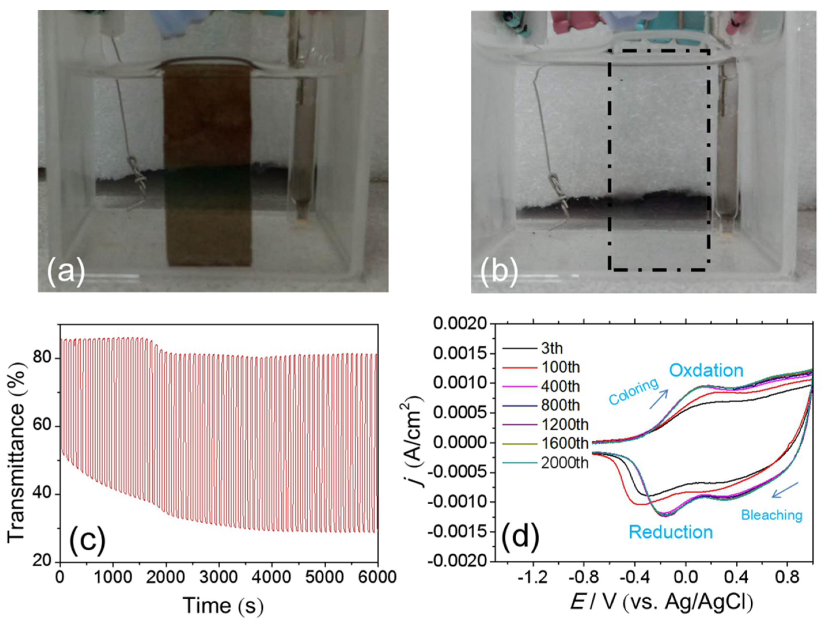
3.3. Cyclic Durability of the NiOx Film with Optimized Parameters

Considering the above optimized parameters, the NiOx film which is spin-coated three times and annealed at 150 °C with the 1:2 ratio in NiOx inks of IPA:DI water gives better ΔT, higher CE and faster switching time. Therefore, we choose the optimized NiOx film for further study. Figure 11a,b shows good contrast between the bleached state and the colored state, the NiOx films exhibit reversible color change from dark brown (colored state) to transparent (bleached state). The optimized NiOx electrode has been tested for applied square-wave-type voltages (±1.0 V, 90 s per cycle) up to 6000 s in 1 M KOH electrolyte. The spectral response at 550 nm has been recorded in Figure 11c. The ΔT of the NiOx film exhibits a value of ΔT = 34.2% for the initial time. It increases gradually and reaches a maximum value of 52.7% in the steady period up to 6000 s. In addition, the cyclic durability limits the further advancement of NiO-based films as has been reported by many researchers, which showed that the degradations are depending on the applied electrolytes or fabrication parameters [13,37]. Therefore, we choose the optimized NiOx electrode to further study its cyclic durability. Because NiO-based films are often used in ECDs containing Li+ electrolytes [38,39], we consider using 0.5 M LiClO4-PC electrolyte for cyclic voltammetry tests (CVs) in Figure 11d. It is usually recognized that NiOx was subjected to the following electrochemical oxidation and reduction processes [13]:
NiO x + yLi + + ye Li y NiO x
Li y NiO x Li y z NiO x + zLi + + ze
Figure 11d showed typical oxidation and reduction peaks. The peak potential shifted in the first few cycles, when the migration paths for ions were established and became stable. This process involved the slight change of thin film resistance, which caused slight change of voltage on the film, and thus the shifting of reduction and oxidation peaks. The peaks became immobile after 400 cycles. The separation between cathodic and anodic peaks of j in the steady periods was smaller than that of the initial periods. It indicated that the NiOx films had higher electrochemical reaction activity in the steady periods. It showed that the optimized NiOx film did not obviously degraded until 2000 cycles, which proved good stability of the optimized NiOx film in Li+-based electrolytes.

4. Conclusions

In summary, NiOx NPs fabricated by chemical precipitation method were developed to prepare IPA-DI water-NiOx suspensions for application of spin-coated NiOx films. The optical properties of EC NiOx films as functions of the number of spin-coating layers, annealing temperature, and the volume ratios of IPA to DI water in IPA-DI water-NiOx suspensions were systematically investigated. Large transmittance of 62.3% at 550 nm, high coloration efficiency (42.8 cm2/C), rapid switching time (coloring time is 4 s, bleaching time is 3 s) and good stability were achieved in the optimized NiOx film, which is characterized by spin-coating three times and 150 °C annealing in air with the 1:2 volume ratio of IPA:DI water. We showed that the NiOx NPs were uniformly and distinctly dispersed in the optimized NiOx film, which facilitated the best ion migration. CVs of the optimized NiOx film in LiClO4-PC electrolyte prove to have good cyclic durability without obvious degradation. The fabrication technique used low-cost and non-toxic precursors with low fabrication temperature, which facilitates further development of fabricating electrochromic devices at low temperatures.

Author Contributions

For the research articles with several authors, Xiaohong Xie, Changkang Gao, Xiang Du, Gangyi Zhu, Weiguang Xie, Pengyi Liu and Zhenfang Tang conceived and designed the study; Xiaohong Xie, Changkang Gao and Xiang Du performed the experiments; Gangyi Zhu, Weiguang Xie, Pengyi Liu and Zhenfang Tang analyzed the data; Weiguang Xie and Zhenfang Tang contributed reagents/materials/analysis tools; Xiaohong Xie wrote the paper. Weiguang Xie reviewed the manuscript. All authors read and approved the manuscript.

Funding

This research was funded by the National Natural Science Foundation of China, grant number 11574119, 61674070, and the Science and Technology Planning Project of Guangdong Province, grant number 2016B020244002.

Conflicts of Interest

The authors declare no conflict of interest.

References

  1. Ma, H.; Du, N.; Yu, S.; Lu, W.; Zhang, Z.; Deng, N.; Li, C. Analysis of typical public building energy consumption in northern China. Energy Build. 2017, 136, 139–150. [Google Scholar] [CrossRef]
  2. Ma, L.; Shao, N.; Zhang, J.; Zhao, T. The Influence of Doors and Windows on the Indoor Temperature in Rural House. Procedia Eng. 2015, 121, 621–627. [Google Scholar] [CrossRef]
  3. Somani, P.R.; Radhakrishnan, S. Electrochromic materials and devices: Present and future. Mater. Chem. Phys. 2003, 77, 117–133. [Google Scholar] [CrossRef]
  4. Drosos, C.; Vernardou, D. Perspectives of energy materials grown by APCVD. Sol. Energy Mater. Sol. Cells 2015, 140, 1–8. [Google Scholar] [CrossRef]
  5. Vernardou, D.; Psifis, K.; Louloudakis, D.; Papadimitropoulos, G.; Davazoglou, D.; Katsarakis, N.; Koudoumas, E. Low pressure CVD of electrochromic WO3 at 400 °C. J. Electrochem. Soc. 2015, 162, H579–H582. [Google Scholar] [CrossRef]
  6. Granqvist, C.; Azens, A.; Hjelm, A.; Kullman, L.; Niklasson, G.A.; Rönnow, D.; Mattsson, M.S.; Veszelei, M.; Vaivars, G. Recent advances in electrochromics for smart windows applications. Sol. Energy 1998, 63, 199–216. [Google Scholar] [CrossRef]
  7. Liang, L.; Zhang, J.; Zhou, Y.; Xie, J.; Zhang, X.; Guan, M.; Pan, B.; Xie, Y. High-performance flexible electrochromic device based on facile semiconductor-to-metal transition realized by WO3·2H2O ultrathin nanosheets. Sci. Rep. 2013, 3, 1936. [Google Scholar] [CrossRef] [PubMed]
  8. Luo, J.Y.; Deng, S.Z.; Tao, Y.T.; Zhao, F.L.; Zhu, L.F.; Gong, L.; Chen, J.; Xu, N.S. Evidence of localized water molecules and their role in the gasochromic effect of WO3 nanowire films. J. Phys. Chem. C 2009, 113, 15877–15881. [Google Scholar] [CrossRef]
  9. Zheng, Z.; Chen, J.; Wang, Y.; Wang, X.; Chen, X.; Liu, P.; Xu, J.; Xie, W.; Chen, H.; Deng, S. Highly Confined and Tunable Hyperbolic Phonon Polaritons in Van Der Waals Semiconducting Transition Metal Oxides. Adv. Mater. 2018, 30, 1705318. [Google Scholar] [CrossRef] [PubMed]
  10. Paulose, R.; Mohan, R.; Parihar, V. Nanostructured nickel oxide and its electrochemical behaviour—A brief review. Nanostruct. Nano-Obj. 2017, 11, 102–111. [Google Scholar] [CrossRef]
  11. Zhou, D.; Xie, D.; Xia, X.; Wang, X.; Gu, C.; Tu, J. All-solid-state electrochromic devices based on WO3|| NiO films: Material developments and future applications. Sci. China Chem. 2017, 60, 3–12. [Google Scholar] [CrossRef]
  12. Cai, G.; Darmawan, P.; Cui, M.; Chen, J.; Wang, X.; Eh, A.L.-S.; Magdassi, S.; Lee, P.S. Inkjet-printed all solid-state electrochromic devices based on NiO/WO3 nanoparticle complementary electrodes. Nanoscale 2016, 8, 348–357. [Google Scholar] [CrossRef] [PubMed]
  13. Liu, Q.; Dong, G.; Xiao, Y.; Delplancke-Ogletree, M.-P.; Reniers, F.; Diao, X. Electrolytes-relevant cyclic durability of nickel oxide thin films as an ion-storage layer in an all-solid-state complementary electrochromic device. Sol. Energy Mater. Sol. Cells 2016, 157, 844–852. [Google Scholar] [CrossRef]
  14. Granqvist, C.G. Handbook of Inorganic Electrochromic Materials; Elsevier: New York, NY, USA, 1995. [Google Scholar]
  15. Ren, Y.; Zhou, X.; Zhang, H.; Lei, L.; Zhao, G. Preparation of a porous NiO array-patterned film and its enhanced electrochromic performance. J. Mater. Chem. C 2018. [Google Scholar] [CrossRef]
  16. Zhou, K.; Qi, Z.; Zhao, B.; Lu, S.; Wang, H.; Liu, J.; Yan, H. The influence of crystallinity on the electrochromic properties and durability of NiO thin films. Surf. Interfaces 2017, 6, 91–97. [Google Scholar] [CrossRef]
  17. Dalavi, D.S.; Devan, R.S.; Patil, R.S.; Ma, Y.-R.; Patil, P.S. Electrochromic performance of sol–gel deposited NiO thin film. Mater. Lett. 2013, 90, 60–63. [Google Scholar] [CrossRef]
  18. Shi, J.; Lai, L.; Zhang, P.; Li, H.; Qin, Y.; Gao, Y.; Luo, L.; Lu, J. Aluminum doped nickel oxide thin film with improved electrochromic performance from layered double hydroxides precursor in situ pyrolytic route. J. Solid State Chem. 2016, 241, 1–8. [Google Scholar] [CrossRef]
  19. Jiang, S.; Yuan, G.; Hua, C.; Khan, S.; Wu, Z.; Liu, Y.; Wang, J.; Song, C.; Han, G. Electrochromic Properties of Ni/NiO/rGO Nanocomposite Films Prepared by a Facile Sol-Gel Technique. J. Electrochem. Soc. 2017, 164, H896–H902. [Google Scholar] [CrossRef]
  20. Zhao, C.; Du, F.; Wang, J. Flower-like nickel oxide micro/nanostructures: Synthesis and enhanced electrochromic properties. RSC Adv. 2015, 5, 38706–38711. [Google Scholar] [CrossRef]
  21. Chen, Y.; Wang, Y.; Sun, P.; Yang, P.; Du, L.; Mai, W. Nickel oxide nanoflake-based bifunctional glass electrodes with superior cyclic stability for energy storage and electrochromic applications. J. Mater. Chem. A 2015, 3, 20614–20618. [Google Scholar] [CrossRef]
  22. Chen, Z.; Xiao, A.; Chen, Y.; Zuo, C.; Zhou, S.; Li, L. Highly porous nickel oxide thin films prepared by a hydrothermal synthesis method for electrochromic application. J. Phys. Chem. Solids 2013, 74, 1522–1526. [Google Scholar] [CrossRef]
  23. Zhang, J.-H.; Cai, G.-F.; Zhou, D.; Tang, H.; Wang, X.-L.; Gu, C.-D.; Tu, J.-P. Co-doped NiO nanoflake array films with enhanced electrochromic properties. J. Mater. Chem. C 2014, 2, 7013–7021. [Google Scholar] [CrossRef]
  24. Cai, G.; Tu, J.; Zhou, D.; Li, L.; Zhang, J.; Wang, X.; Gu, C. Constructed TiO2/NiO core/shell nanorod array for efficient electrochromic application. J. Phys. Chem. C 2014, 118, 6690–6696. [Google Scholar] [CrossRef]
  25. Lou, X.; Zhao, X.; He, X. Boron doping effects in electrochromic properties of NiO films prepared by sol–gel. Sol. Energy 2009, 83, 2103–2108. [Google Scholar] [CrossRef]
  26. Tenent, R.C.; Gillaspie, D.T.; Miedaner, A.; Parilla, P.A.; Curtis, C.J.; Dillon, A.C. Fast-switching electrochromic Li+-doped NiO films by ultrasonic spray deposition. J. Electrochem. Soc. 2010, 157, H318–H322. [Google Scholar] [CrossRef]
  27. Lang, F.; Liu, J.; Wang, H.; Yan, H. NiO Nanocrystalline/Reduced Graphene Oxide Composite Film with Enhanced Electrochromic Properties. Nano 2017, 12, 1750058. [Google Scholar] [CrossRef]
  28. Cai, G.-F.; Tu, J.-P.; Zhang, J.; Mai, Y.-J.; Lu, Y.; Gu, C.-D.; Wang, X.-L. An efficient route to a porous NiO/reduced graphene oxide hybrid film with highly improved electrochromic properties. Nanoscale 2012, 4, 5724–5730. [Google Scholar] [CrossRef] [PubMed]
  29. Talebian, N.; Kheiri, M. Sol–gel derived nanostructured nickel oxide films: effect of solvent on crystallographic orientations. Solid State Sci. 2014, 27, 79–83. [Google Scholar] [CrossRef]
  30. Jiang, F.; Choy, W.C.; Li, X.; Zhang, D.; Cheng, J. Post-treatment-Free Solution-Processed Non-stoichiometric NiOx Nanoparticles for Efficient Hole-Transport Layers of Organic Optoelectronic Devices. Adv. Mater. 2015, 27, 2930–2937. [Google Scholar] [CrossRef] [PubMed]
  31. Birks, L.; Friedman, H. Particle size determination from X-ray line broadening. J. Appl. Phys. 1946, 17, 687–692. [Google Scholar] [CrossRef]
  32. Sun, D.-L.; Zhao, B.-W.; Liu, J.-B.; Wang, H.; Yan, H. Application of nickel oxide nanoparticles in electrochromic materials. Ionics 2017, 23, 1509–1515. [Google Scholar] [CrossRef]
  33. Ma, D.; Wang, J. Inorganic electrochromic materials based on tungsten oxide and nickel oxide nanostructures. Sci. China Chem. 2017, 60, 54–62. [Google Scholar] [CrossRef]
  34. Sahu, D.; Wu, T.-J.; Wang, S.-C.; Huang, J.-L. Electrochromic behavior of NiO film prepared by e-beam evaporation. J. Sci. Adv. Mater. Devices 2017, 2, 225–232. [Google Scholar] [CrossRef]
  35. Atak, G.; Coşkun, Ö.D. Annealing effects of NiO thin films for all-solid-state electrochromic devices. Solid State Ionics 2017, 305, 43–51. [Google Scholar] [CrossRef]
  36. Zhou, K.; Wang, H.; Zhang, Y.; Liu, J.; Yan, H. An advanced technique to evaluate the electrochromic performances of NiO films by multi-cycle double-step potential chronocoulometry. J. Electrochem. Soc. 2016, 163, H1033–H1040. [Google Scholar] [CrossRef]
  37. Hou, S.; Zhang, X.; Tian, Y.; Zhao, J.; Geng, H.; Qu, H.; Zhang, H.; Zhang, K.; Wang, B.; Gavrilyuk, A. Improved Electrochemical Cycling Durability in a Nickel Oxide Double-Layered Film. Chem. Asian J. 2017, 12, 2922–2928. [Google Scholar] [CrossRef] [PubMed]
  38. Patel, K.; Bhatt, G.; Ray, J.; Suryavanshi, P.; Panchal, C. All-inorganic solid-state electrochromic devices: A review. J. Solid State Electrochem. 2017, 21, 337–347. [Google Scholar] [CrossRef]
  39. Zhou, J.; Luo, G.; Wei, Y.; Zheng, J.; Xu, C. Enhanced electrochromic performances and cycle stability of NiO-based thin films via Li–Ti co-doping prepared by sol–gel method. Electrochim. Acta 2015, 186, 182–191. [Google Scholar] [CrossRef]
Figure 1. Preparation flowchart of NiOx NPs and NiOx films.
Materials 11 00760 g001
Figure 2. XRD pattern of NiOx NPs fabricated by chemical precipitation method.
Materials 11 00760 g002
Figure 3. Optical transmittance spectra at as-deposited, colored and bleached states of NiOx films as a function of the number of spin-coating layers: (a) spin-coating once; (b) spin-coating three times; (c) spin-coating five times; (d) spin-coating seven times (the increases of voltages has little effect on the Tb, so the 2 bleached curves overlap together); (e) ΔOD; (f) Switching curve of the NiOx film by spin-coating three times. The NiOx films are annealed at 100 °C and the volume ratio in NiOx inks is IPA:DI water = 1:3.
Materials 11 00760 g003
Figure 4. Optical transmittance spectra at as-deposited, colored and bleached states of the NiOx films as a function of annealing temperature: (a) RT; (b) 100 °C; (c) 150 °C; (d) 200 °C; (e) 300 °C (The increases of voltage has little effect on the Tb, so the 2 bleached curves overlap together) and (f) ΔOD. The NiOx films are spin-coated three times and the volume ratio in NiOx inks is IPA:DI water = 1:3.
Materials 11 00760 g004
Figure 5. SEM images of NiOx films after (a) RT; (b) 150 °C and (c) 300 °C annealing. The NiOx films are spin-coated three times and the volume ratio in NiOx inks is IPA:DI water = 1:3. The red arrows indicate the voids.
Materials 11 00760 g005
Figure 6. CVs of the NiOx films annealed at RT, 100 °C and 150 °C in 1 M KOH electrolyte. The NiOx films are spin-coated three times and the volume ratio in NiOx inks is IPA:DI water = 1:3.
Materials 11 00760 g006
Figure 7. Optical transmittance spectra at as-deposited, colored and bleached states of NiOx films as a function of the volume ratios of IPA:DI water in NiOx inks: (a) 0:1; (b) 1:3; (c) 1:2; (d) 1:1 and (e) 2:1 (The increases of voltage has little effect on the Tb, so the 2 bleached curves overlap together) and (f) ΔOD. The NiOx thin films are by spin-coating three times and after 150 °C annealing.
Materials 11 00760 g007
Figure 8. Switching curves of NiOx films as a function of the volume ratios of IPA:DI water in NiOx inks: (a) 0:1; (b) 1:3; (c) 1:2; (d) 1:1 and (e) 2:1. The NiOx films are by spin-coating three times and after 150 °C annealing.
Materials 11 00760 g008
Figure 9. SEM images of NiOx films in different volume ratios of IPA:DI water in NiOx inks: (a) 0:1; (b) 1:3; (c) 1:2; (d) 1:1 and (e) 2:1. The NiOx films are by three times spin-coating and after 150 °C annealing.
Materials 11 00760 g009
Figure 10. CVs of the NiOx films in different volume ratios of IPA:DI water in NiOx inks in 1 M KOH electrolyte. The NiOx films are spin-coated three times and annealed to 150 °C.
Materials 11 00760 g010
Figure 11. (a) Optical images of the colored and bleached states; (b) Optical images of the colored and bleached states; (c) cycles of optical switching for the optimized sample in 1 M KOH electrolyte and (d) CVs of the optimized NiOx film in 0.5 M LiClO4-PC electrolyte.
Materials 11 00760 g011
Table 1. NiO-based films reported earlier by chemical solution methods in KOH electrolyte.
No.MethodsFilmsAnnealing ConditionΔT
(%)
CE
(cm2/C)
Tc/Tb
(s)
Ref.Year
1Dip-coating NiO film500 °C51407/5[15]2017
2Dip-coating NiO film350 °C50.771.4-[16]2017
3Inkjet printingNiO film200 °C64.2136.79/6[12]2016
4Hydrothermal NiO film 300 °C35.849.81.3/3.2[20]2015
5HydrothermalNiO film 400 °C/Ar4063.22.7/1.8[21]2015
6Hydrothermal NiO film300 °C/Ar77493/4[22]2013
7Spin-coating Al-doped NiO film400 °C58.454.24.2/1.8[18]2016
8CBDCo-doped NiO film300 °C88.347.75.4/3.4[23]2014
9Dip-coating NiO/GO film350 °C40.712.854.3/3.9[27]2017
10Spin-coating Ni/NiO/rGO film350 °C/N2 and air51.648.154.2/2.4[19]2017
11CBDTiO2/NiO film300 °C/Ar8360.66.8/14.8[24]2014
12Spin-coatingNiOx film150 °C/air62.342.84/3This work

