A Semi-Analytical Extraction Method for Interface and Bulk Density of States in Metal Oxide Thin-Film Transistors
by
 and
and
Weifeng Chen
1, 
Weijing Wu
1,*,
Lei Zhou
2,
Miao Xu
1,
Lei Wang
1,
Honglong Ning
1 and
Junbiao Peng
1 1
State Key Laboratory of Luminescent Materials and Devices, South China University of Technology, Guangzhou 510640, China
2
Guangzhou New Vision Opto-Electronic Technology Co., Ltd., Guangzhou 510530, China
*
Author to whom correspondence should be addressed.
Materials 2018, 11(3), 416; https://doi.org/10.3390/ma11030416
Submission received: 24 January 2018
/
Revised: 25 February 2018
/
Accepted: 8 March 2018
/
Published: 11 March 2018
Abstract
:A semi-analytical extraction method of interface and bulk density of states (DOS) is proposed by using the low-frequency capacitance–voltage characteristics and current–voltage characteristics of indium zinc oxide thin-film transistors (IZO TFTs). In this work, an exponential potential distribution along the depth direction of the active layer is assumed and confirmed by numerical solution of Poisson’s equation followed by device simulation. The interface DOS is obtained as a superposition of constant deep states and exponential tail states. Moreover, it is shown that the bulk DOS may be represented by the superposition of exponential deep states and exponential tail states. The extracted values of bulk DOS and interface DOS are further verified by comparing the measured transfer and output characteristics of IZO TFTs with the simulation results by a 2D device simulator ATLAS (Silvaco). As a result, the proposed extraction method may be useful for diagnosing and characterising metal oxide TFTs since it is fast to extract interface and bulk density of states (DOS) simultaneously.
1. Introduction
Thin film transistors (TFTs) are one kind of field-effect transistors (FETs). Their structure and operation principles are similar to those of metal oxide semiconductor field effect transistors (MOSFETs), which are commonly used in modern integrated circuits (ICs) [1]. Amorphous oxide semiconductor thin-film transistors (AOS TFTs) are considered one of the most promising technologies for flat panel display (FPD) due to transparency, good uniformity, higher mobility than hydrogenated amorphous silicon TFTs (a-Si:H TFTs), good process compatibility with a-Si TFTs, and a lower temperature fabrication process than low temperature poly-silicon (LTPS) TFTs [2,3,4,5]. The electrical characteristics of AOS TFTs are significantly affected by the bulk density of states (DOS) in the active layer and the interface density of states between the gate insulator and the active layer. The bulk DOS may be attributed to structural disorder (bond angles and length variations), dangling bonds, non-stoichiometry, and carrier scattering in the amorphous films [6]. The interface DOS may be caused by defects located at the interface, which can exchange charge with the active layers by capturing or emitting electrons [7]. It is important to extract DOS of TFTs for device design, process characterization, or modeling. Several methods have been developed to extract only the bulk DOS, such as numerical calculations [8], optical illumination [9], temperature-dependent characteristics [10], or multi-frequency current–voltage (C–V) characteristics [11]. However, it is usually difficult to extract the interface DOS and the bulk DOS simultaneously.
Lui et al. [12] and Kimura [13] extracted the interface and bulk density of states in TFTs from the characteristics of capacitance–voltage and current–voltage based on the numerical iterative solution of Poisson’s equation. However, the numerical iterative solution generally has the disadvantages of operation complexity, long computational time, and possible convergence problems. Hastas et al. extracted interface trap states from analysis of the transfer characteristics in the sub-threshold region and the bulk trap states by numerically fitting the surface potential equation [14]. Tsuji et al. extracted the interface trap density based on an expression of interface trap charge density (Qit) as functions of the front and back-side surface potentials, in which the electric field at the back side is assumed to be zero [15]. Therefore, it is essential to develop analytical methods for extracting both the interface DOS and the bulk DOS of TFTs.
In this work, we propose a semi-analytical method to extract the interface DOS and the bulk DOS in indium zinc oxide (IZO) TFTs simultaneously by only using the low-frequency capacitance–voltage characteristics and current–voltage characteristics.
2. Extraction Method
Figure 1a shows a schematic cross-sectional view of indium zinc oxide (IZO) TFTs with inverted staggered bottom gate structure. The IZO material as the channel layer has the advantages of transparency, high mobility, and excellent drain current saturation [16]. Figure 1b shows the energy band diagram of the device, in which the surface potential (Ψs) and the back interface potential (Ψb) are respectively labeled. Poisson’s equation is given by
where nfree(x) and ntrap(x) are the free electron concentration and localised trapped electron concentration, respectively.
Using the relationship , we can get
Substituting Equation (1) into Equation (2) and differentiating both sides with respect to Ψ, we have
where ρ(Ψs) is the surface charge concentration, and ρ(Ψb) is the back interface charge concentration. Equations (3) and (4) can be further rearranged as
Based on Gauss’s theorem, the surface charge per unit area in the channel (Qs) considering the effect of the back interface potential can be expressed as
In this paper, the potential distribution along the depth direction (x) of the active layer is assumed as
where x0 is the characteristic length of the potential distribution. Note that the assumption for Equation (8) will be confirmed by the numerical solution of Poisson’s equation in Appendix A and the device simulation in Section 3. Substituting Equation (8) into Equations (5)–(7), we have
While in [12], the surface charge at the back interface was not taken into account.
The differential of surface potential with respect to gate-source bias can be expressed as [17]
where Cg(Vgs) is gate capacitance at some Vgs, Cox is the gate oxide capacitance per unit area, and Qg is the charge per unit area at the gate electrode
The nonlinear relation between Ψs and Vgs can be obtained by integrating Equation (12) over Vgs:
where Vfb is the flat band voltage.
The free charge density per unit area (Qi) can be expressed by an integration of nfree(x) over x.
where ts is the thickness of the active layer, n0 is the flat band electron concentration, and Vt is the thermal voltage (kT/q). On the other hand, Qi can also be obtained from the transfer characteristics of TFT at low Vds.
Note that n0 can be extracted from Equation (15) equal to Equation (16) at the condition of flat band, i.e., Ψs = 0 and Vgs = Vfb. Then, x0 at some Vgs can be calculated from Equation (15) equal to Equation (16) by numerical integration.
Furthermore, based on the charge conservation relationship Qg + Qo + Qs = 0, where Qo is the effective interface charge per unit area at the gate insulator, one obtains
Thus, the interface density of states (Nit) can be calculated by differentiating Q0 with respect to Ψs
where EF0 is the bulk Fermi level of the active layer, which is calculated from the relationship of n0 to EF0 :
where NC is the effective density of states in the conduction band with a typical value of 5 × 1018 cm−3 [18].
Furthermore, based on the surface potential Ψs given by Equation (14) and the surface charge concentration ρ(Ψs) given by Equation (9), the bulk density of states can be given by [17]
The extraction procedure of DOS is described as follows. Firstly, Ψs with respect to Vgs is obtained from the Cg–Vgs characteristics of TFTs by Equation (14). Secondly, x0 can be calculated from the current characteristics of TFTs by using Equations (15) and (16). Thirdly, ρ(Ψs), Qs, and Qo will be subsequently obtained by Equations (9), (11), and (17), respectively. Finally, the interface density of states (Nit(E)) and the bulk density of states (Nbt(E)) can be extracted by Equations (18) and (20), respectively. As a result, the extraction method may be easily realised step by step as seen from the above extraction procedure.
3. Results and Discussion
The fabrication process of the IZO TFTs is described as follows. A gate electrode of molybdenum (Mo, 200 nm) is deposited by direct current (DC) sputtering. Subsequently, a 300 nm gate insulator (SiO2) was deposited by plasma-enhanced chemical vapor deposition (PECVD). A 30 nm IZO active layer is deposited by using a radio frequency (RF) magnetron system with the segregated target of IZO (In2O3:ZnO = 1:1). Then, an etch stopper layer (ESL) SiO2 is deposited by PECVD to protect the active layer. Finally, a 200nm Mo is formed by sputtering as S/D electrodes. The channel length and width of IZO TFTs are determined by layout and patterned by the conventional lithographic techniques.
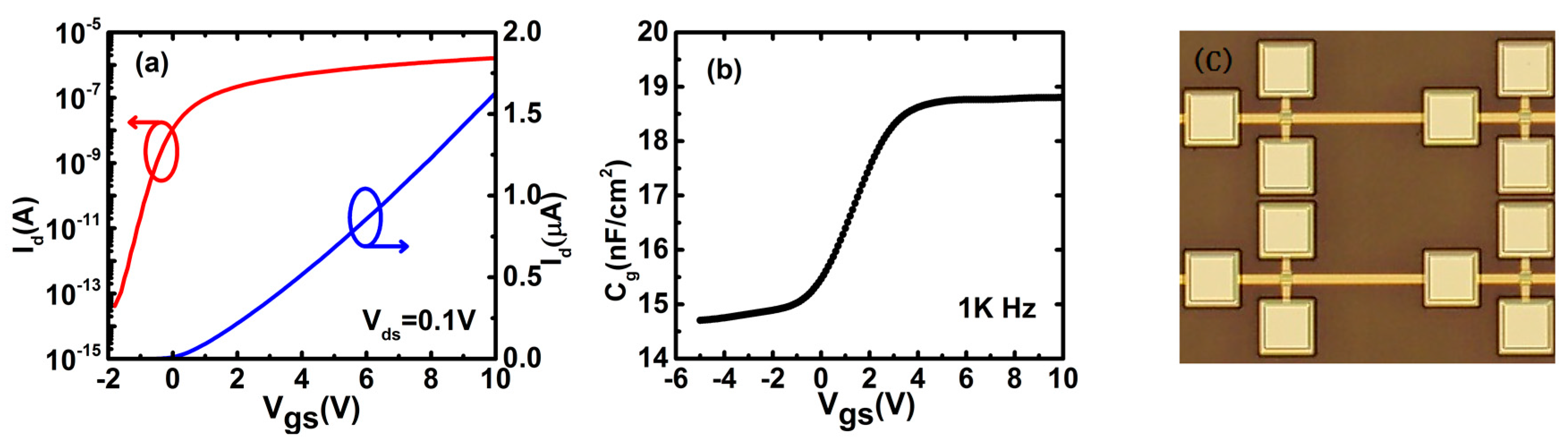
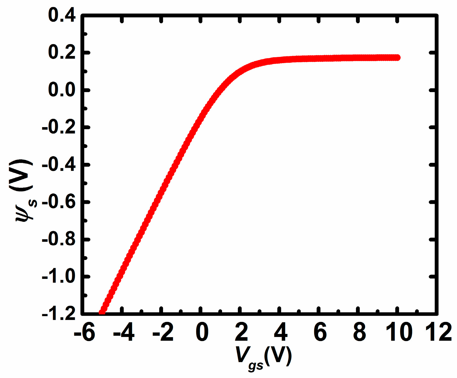
The current–voltage (I–V) and C–V characteristics of TFTs are measured by using a probe station and a semiconductor parameter analyser (Agilent B1500, Agilent Technologies Inc., Santa Clara, CA, USA). The transfer characteristics are measured by scanning the gate-source voltage (Vgs) from −10 V to 10 V with the step of 0.1 V at the condition of Vds = 0.1 V. The C–V characteristics are measured by superimposing the AC voltage signal (amplitude = 200 mV, frequency = 1 kHz) to DC gate bias in the condition of source and drain electrodes connected together. Note that those measurements are done at room temperature in the dark air ambient. It is thought that the DOS distribution of AOS TFTs remains unchanged at different temperatures [10]. Figure 2a shows the transfer characteristics of IZO TFTs (W/L = 20 μm/10 μm). The threshold voltage, the field-effect mobility, sub-threshold swing (SS), and on/off current ratio (Ion/Ioff) of the pristine TFTs are extracted to be 1.8 V, 12.36 cm2/(V·s), 0.23 V/dec, and 1 × 10⁷, respectively. Vfb is extracted as 0.6 V from the I–V characteristics following the method developed by Migliorato et al. [19]. n0 is extracted as 3.84 × 1016 cm−3 by (15) when Ψs = 0, i.e., Vgs = Vfb. Figure 2b shows the Cg–Vgs characteristics of the devices at the frequency of 1 kHz, which are measured with source and drain electrodes combined together. Note that the frequency of 1 kHz for the AC signal may be low enough to make the TFTs work in the quasi-static conditions. Figure 3 shows the surface potential (Ψs) with respect to Vgs from (14) based on the C–V characteristics and the value of Vfb. Figure 2c shows the micrograph of IZO TFTs with W/L = 20 μm/10 μm.
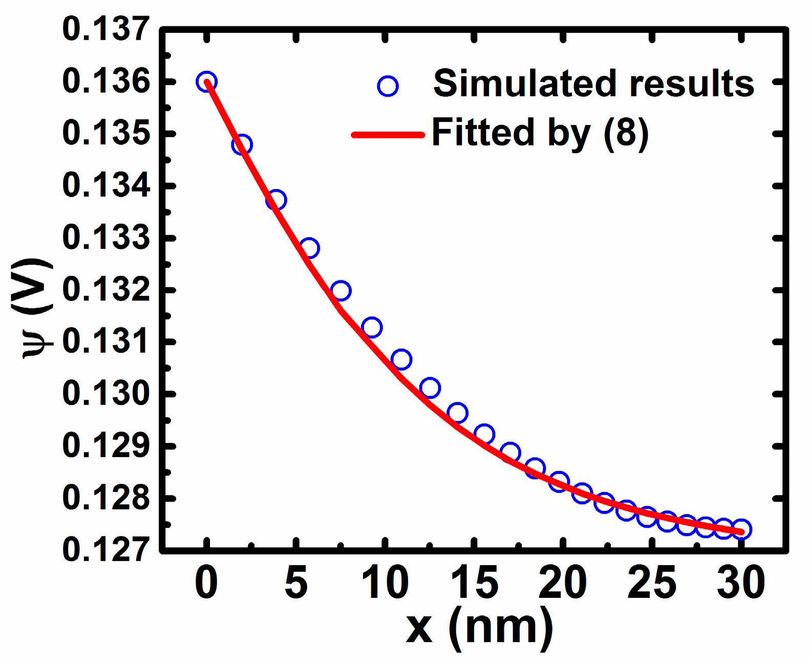
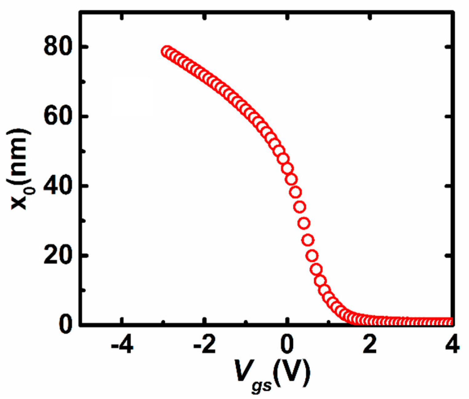
For further verification of (8), we perform the device simulation by the 2D device simulator ATLAS (Silvaco) for the IZO TFTs as described above. Figure 4 shows the distribution of the potential along the depth direction (x) at the conditions of Vgs = 2.0 V, Vds = 0.1 V. It is found that the proposed Equation (8) can fit the simulated potential distribution well. Note that at other values of Vgs including that at the subthreshold region, the simulated potential distributions are also found to be well fitted by Equation (8) with different values of x0. As a result, Equation (8) may be reasonable and correct for reproducing the potential distribution of the thin active layer. Furthermore, based on the I–V characteristics and the surface potential distribution as seen in Figure 3, the value of x0 can be extracted from Equation (15) equal to Equation (16), as shown in Figure 5. It is found that the value of x0 tends to vary slowly when Vgs is larger than the threshold voltage, because the variation of Qi changes more slowly for TFTs working in the above-threshold region.
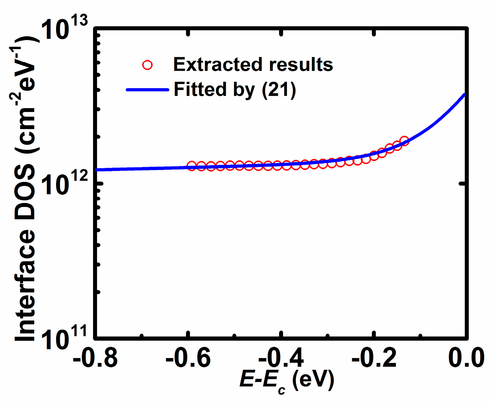
Figure 6 shows the extracted interface density of states profile calculated from Equation (18). It is found that the interface DOS distribution is quite flat for the energy far from EC, while it linearly increases with the increase of energy close to EC at the exponent coordinate. Then, the interface DOS of AOS TFTs may be divided into two parts: constant deep states and exponential tail states, i.e.,
where NiD is the density of deep states, NiT is the density tail states at the conduction edge, and EiT is the characteristic energy of tail states. For details, NiD/NiT is extracted by extrapolating the deep/tail states to E = EC, and EiT is extracted from the slope of log(Nit) versus (E − EC) for the tail states. The extracted values are NiD = 1.3 × 1012 cm−2 eV−1, NiT = 2.9 × 1012 cm−2 eV−1, EiT = 0.08 eV. Obviously, the interface DOS distribution can be used to characterise interface quality and the reliability of AOS TFTs [20,21].
Figure 7 shows the bulk density of states profile extracted from Equation (20). It is observed that the bulk DOS distribution slowly increases with the increase of the energy far from EC, while it quickly increases with the increase of energy close to EC at the exponent coordinate. It is found that the bulk DOS may be a superposition of exponential deep states and exponential tail states, i.e.,
where NbD/NbT is the density of deep/tail states at the conduction edge and EbD/EbT is the characteristic energy of deep/tail states, of which the extraction method is similar to that of interface DOS as described above. The extracted values are NbD = 6.0 × 1016 cm−3 eV−1, EbD = 5.0 eV, NbT = 6.5 × 1017 cm−3 eV−1, and EbT = 0.10 eV. Such double exponential distribution for the bulk DOS can also be seen in other previously reported works [8,9,10,11]. For details, the deep states in AOSs may derive from oxygen deficiency, while the tail states originate from the variation of In–O–metal bonding angles [22].
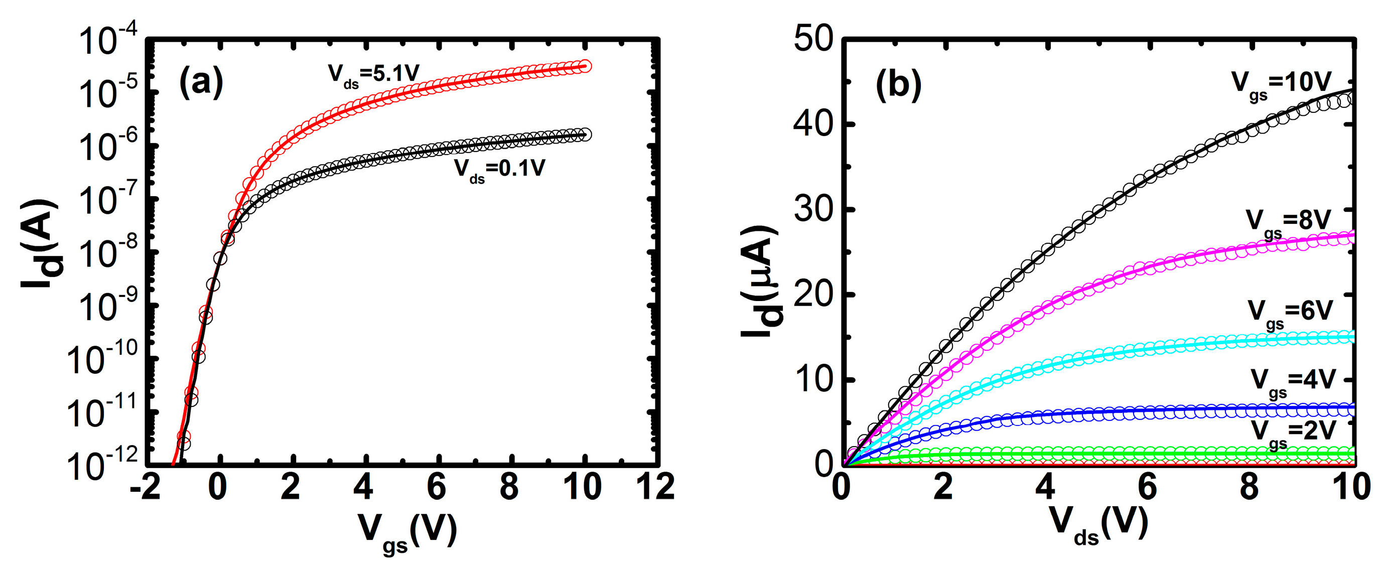
The device simulation is performed by a 2D device simulator ATLAS (Silvaco, Silvaco International, Santa Clara, CA, USA) to verify the proposed method, where the extracted values of interface DOS and bulk DOS are inserted into the simulator. The other parameters of IZO TFTs in the simulation are the same as those of the fabricated IZO TFTs. As seen from Figure 8, the simulation results exhibit a good agreement with the measured transfer and output characteristics of IZO TFTs. In brief, the proposed extraction method for interface and bulk DOS is valuable for the application in metal oxide TFTs.
4. Conclusions
In this paper, we propose a semi-analytical extraction method for the interface DOS and the bulk DOS of IZO TFTs by using the low-frequency C–V characteristics and I–V characteristics. It is shown that the interface DOS is extracted as a superposition of constant deep states and exponential tail states with NiD = 1.3 × 1012 cm−2 eV−1, NiT = 2.9 × 1012 cm−2 eV−1, and EiT = 0.08 eV. Additionally, the bulk DOS is extracted as the superposition of exponential deep states and exponential tail states with NbD = 6.0 × 1016 cm−3 eV−1, EbD = 5.0 eV, NbT = 6.5 × 1017 cm−3 eV−1, and EbT = 0.10 eV. Furthermore, the device simulation is performed by a 2D device simulator to verify the extracted values of interface DOS and bulk DOS. It is found that there is a good agreement between simulation results and the measured transfer and output characteristics of IZO TFTs. Hence, the proposed extraction method for interface and bulk DOS may be valuable for characterising metal oxide TFTs due to the advantages of being semi-analytical and fast. Since the proposed extraction method is directly deduced from Poisson’s equation, it may also be applied in other types of TFTs, such as a-Si:H TFTs, polysilicon TFTs, or organic TFTs.
Acknowledgments
This work was supported in part by the National Key Research and Development Program of China under Grant 2016YFB0401005, in part by National Natural Science Foundation of China under Grants 61574062 and 61574061, in part by Science and Technology Program of Guangdong Province under Grants 2016B090906002, 2016B090907001, 2017B090901055, and 2017B090901006, in part by Pear River S&T Nova Program of Guangzhou under Grant 201506010015, in part by Tiptop Scientific and Technical Innovative Youth Talents of Guangdong Special Support Program under Grant 2014TQ01C321, in part by the Fundamental Research Funds for the Central Universities under Grant 2017ZD059.
Author Contributions
Wei-feng Chen and Wei-jing Wu developed the extraction methods, Lei Zhou analysed the data, Miao Xu and Lei Wang fabricated the TFTs, Hong-long Ning and Jun-Biao Peng supervised the projects.
Conflicts of Interest
The authors declare no conflict of interest.
Appendix A
Poisson’s equation is rewritten by
where nfree(x) and ntrap(x) may be expressed as
Note that, Equation (A2) represents the electron concentration varying with surface band bending [7].
Substituting (22) into (A3) and integrating, we have
with
Then, substituting (A2) and (A4) into (A1), yields
Obviously, there is no analytical solution for (A5) due to its complexity. Hence, a numerical iterative solution for (A5) should be used to observe the distribution of potential.
Under the boundary conditions
where Ψs is obtained from (14). Es is the surface electric field of the active layer, which is obtained from the relationships and , where Vox is the voltage across the oxide and Φms is the work function difference between the gate and active layer semiconductor.
Then
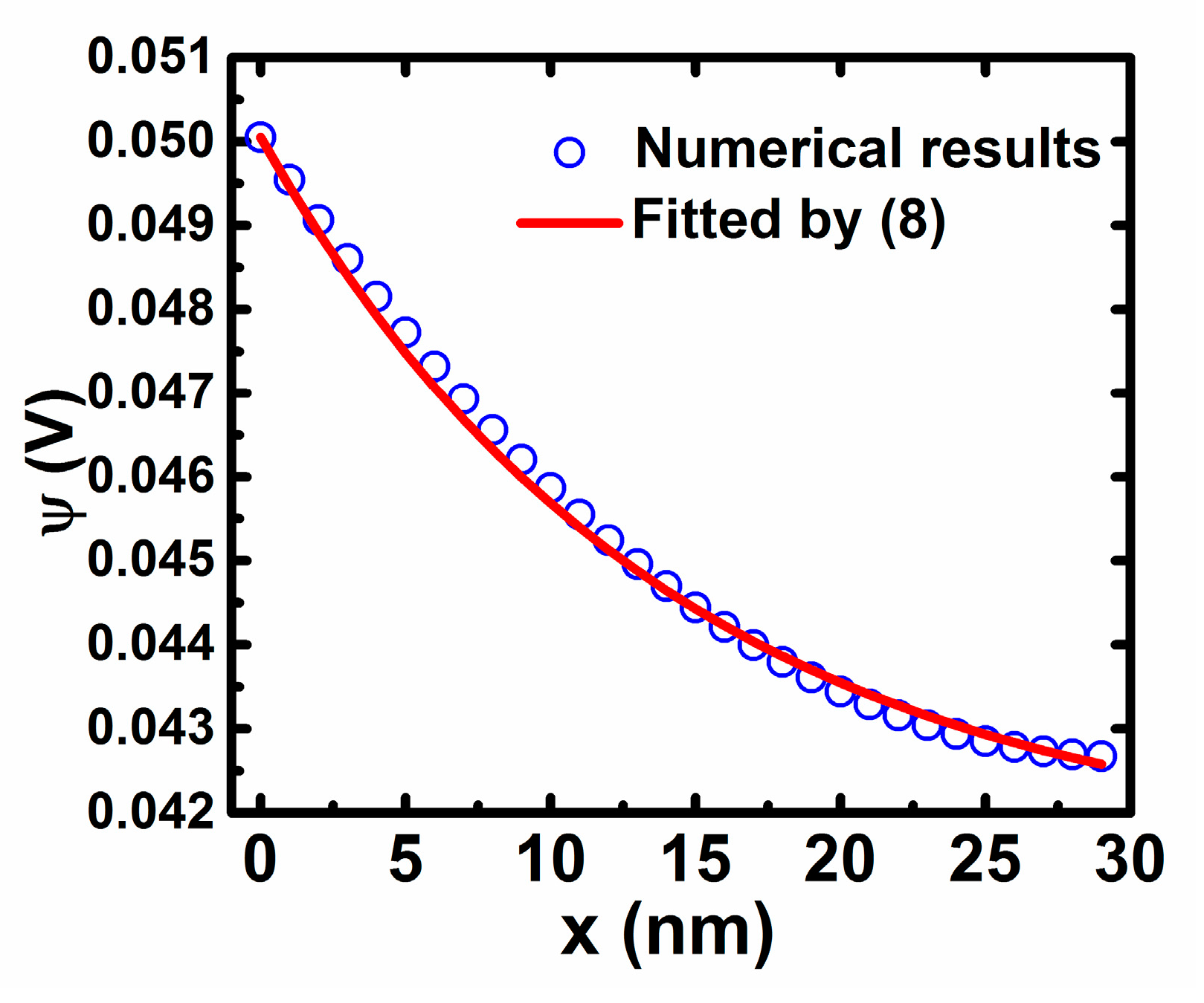
As a result, Poisson’s equation of (A5) can be numerically solved under the boundary conditions of (A6) by using the conventional finite difference method. Figure A1 shows the numerical results of the potential along the depth direction (x) with the extracted values of Nbt(E) at the condition of Vgs = 1.0 V. It is shown that the numerical results of potential distribution may be reproduced well by (8). It is further found that the numerical results of potential distribution at other Vgs can also be fitted well by (8) with different x0. Similarly, analytical complex exponential distributions of potential are also obtained by only taking into account either the free electrons [23] or the trapped electrons [12] in Poisson’s equation. In brief, Equation (8) may be a reasonable approximation for the potential distribution to achieve a good tradeoff between accuracy and simplicity.
Figure A1.
The potential distribution by numerical solution for (A5).

References
- Yue, K. Thin film transistor technology—Past, present, and future. Electrochem. Soc. Interface 2013, 22, 55–61. [Google Scholar]
- Nomura, K.; Ohta, H.; Takagi, A.; Kamiya, T.; Hirano, M.; Hosono, H. Room-temperature fabrication of transparent flexible thin-film transistors using amorphous oxide semiconductors. Nature 2004, 432, 488–492. [Google Scholar] [CrossRef] [PubMed]
- Park, J.S.; Maeng, W.-J.; Kim, H.-S.; Park, J.-S. Review of recent developments in amorphous oxide semiconductor thin-film transistor devices. Thin Solid Films 2012, 520, 1679–1693. [Google Scholar] [CrossRef]
- Lin, Z.; Lan, L.; Xiao, P.; Sun, S.; Li, Y.; Song, W.; Gao, P.; Wang, L.; Ning, H.; Peng, J. High-mobility thin film transistors with neodymium—Substituted indium oxide active layer. Appl. Phys. Lett. 2015, 107, 112108. [Google Scholar] [CrossRef]
- Sheng, J.; Lee, H.-J.; Oh, S.; Park, J.-S. Flexible and high-performance amorphous indium zinc oxide thin-film transistor using low-temperature atomic layer deposition. ACS Appl. Mater. Interfaces 2016, 8, 33821–33828. [Google Scholar] [CrossRef] [PubMed]
- Yu, E.K.-H.; Jun, S.; Kim, D.H.; Kanicki, J. Density of states of amorphous In-Ga-Zn-O from electrical and optical characterization. J. Appl. Phys. 2014, 116, 154505. [Google Scholar] [CrossRef]
- Nicollian, E.H.; Brews, J.R. MOS (Metal Oxide Semiconductor) Physics and Technology; Wiley–Interscience: New York, NY, USA, 1982. [Google Scholar]
- Kimura, M.; Nakanishi, T.; Nomura, K.; Kamiya, T.; Hosono, H. Trap densities in amorphous-InGaZnO4 thin-film transistors. Appl. Phys. Lett. 2008, 92, 133512. [Google Scholar] [CrossRef]
- Bae, H.; Choi, H.; Jun, S.; Jo, C.; Kim, Y.H.; Hwang, J.S.; Ahn, J.; Oh, S.; Bae, J.-U.; Choi, S.-J.; et al. Single-scan monochromatic photonic capacitance-voltage technique for extraction of subgap DOS over the bandgap in amorphous semiconductor TFTs. IEEE Electron Dev. Lett. 2013, 34, 1524–1526. [Google Scholar] [CrossRef]
- Chen, C.; Abe, K.; Kumomi, H.; Kanicki, J. Density of states of a-InGaZnO from temperature-dependent field-effect studies. IEEE Trans. Electron Dev. 2009, 56, 1177–1183. [Google Scholar] [CrossRef]
- Lee, S.; Park, S.; Kim, S.; Jeon, Y.; Jeon, K.; Park, J.-H.; Park, J.; Song, I.; Kim, C.J.; Park, Y.; et al. Extraction of subgap density of states in amorphous InGaZnO thin-film transistors by using multifrequency capacitance-voltage characteristics. IEEE Electron Dev. Lett. 2010, 31, 231–233. [Google Scholar]
- Lui, O.K.B.; Tam, S.W.B.; Migliorato, P.; Shimoda, T. Method for the determination of bulk and interface density of states in thin-film transistors. J. Appl. Phys. 2001, 89, 6453–6458. [Google Scholar] [CrossRef]
- Kimura, M. Extraction technique of trap densities in thin films and at insulator interfaces of thin-film transistors. IEEE Electron Dev. Lett. 2010, 31, 570–572. [Google Scholar] [CrossRef]
- Hastas, N.A.; Tassis, D.H.; Dimitriadis, C.A.; Kamarinos, G. Determination of interface and bulk traps in the subthreshold region of polycrystalline silicon thin-film transistors. IEEE Trans. Electron Dev. 2003, 50, 1991–1994. [Google Scholar] [CrossRef]
- Tsuji, H.; Kamakura, Y.; Taniguchi, K. Simple extraction method of interface trap density in thin-film transistors. J. Electrochem. Soc. 2009, 156, H430–H433. [Google Scholar] [CrossRef]
- Dehuff, N.L.; Kettenring, E.S.; Hong, D.; Chiang, H.Q.; Wager, J.F.; Hoffman, R.L.; Park, C.H.; Keszler, D.A. Transparent thin-film transistors with zinc indium oxide channel layer. J. Appl. Phys. 2005, 97, 064505. [Google Scholar] [CrossRef]
- Wu, W.-J.; Chen, C.-L.; Hu, X.; Xia, X.-H.; Zhou, L.; Xu, M.; Wang, L.; Peng, J.-B. Analytical extraction method for density of states in metal oxide thin-film transistors by using low-frequency capacitance-voltage characteristics. J. Disp. Technol. 2016, 12, 888–891. [Google Scholar] [CrossRef]
- Fung, T.-C.; Chuang, C.-S.; Chen, C.; Abe, K.; Cottle, R.; Townsend, M.; Kumomi, H.; Kanicki, J. Two-dimensional numerical simulation of radio frequency sputter amorphous In-Ga-Zn-O thin-film transistors. J. Appl. Phys. 2009, 106, 084511. [Google Scholar] [CrossRef]
- Migliorato, P.; Seok, M.; Jang, J. Determination of flat band voltage in thin film transistors: The case of amorphous-indium gallium zinc oxide. Appl. Phys. Lett. 2012, 100, 073506. [Google Scholar] [CrossRef]
- Park, J.S.; Kim, H.; Kim, I.D. Overview of electroceramic materials for oxide semiconductor thin film transistors. J. Electroceram. 2014, 32, 117–140. [Google Scholar] [CrossRef]
- Conley, J.F. Instabilities in oxide semiconductor transparent thin film transistors. In Proceedings of the 2009 IEEE International Integrated Reliability Workshop Final Report, South Lake Tahoe, CA, USA, 18–22 October 2009; pp. 50–55. [Google Scholar]
- Hsieh, H.-H.; Kamiya, T.; Nomura, K.; Hosono, H.; Wu, C.-C. Modeling of amorphous ingazno(4) thin film transistors and their subgap density of states. Appl. Phys. Lett. 2008, 92, 133503. [Google Scholar] [CrossRef]
- Kimura, M.; Takizawa, T.; Inoue, S.; Shimoda, T. Analytical current-voltage model for polycrystalline-silicon thin-film transistors. Appl. Phys. Lett. 2002, 80, 2326–2328. [Google Scholar] [CrossRef]
Figure 1.
(a) Cross-sectional view of indium zinc oxide thin-film transistors (IZO TFTs) with inverted staggered bottom gate structure; (b) energy band diagram along the thin-film depth direction of IZO TFTs.
Figure 1.
(a) Cross-sectional view of indium zinc oxide thin-film transistors (IZO TFTs) with inverted staggered bottom gate structure; (b) energy band diagram along the thin-film depth direction of IZO TFTs.

Figure 2.
Experimental data of IZO TFTs (W/L = 20 μm/10 μm). (a) Transfer characteristics; (b) Cg–Vgs characteristics; (c) The micrograph of the devices.
Figure 2.
Experimental data of IZO TFTs (W/L = 20 μm/10 μm). (a) Transfer characteristics; (b) Cg–Vgs characteristics; (c) The micrograph of the devices.

Figure 3.
Ψs versus Vgs obtained by (14) based on the capacitance–voltage (C–V) characteristics.

Figure 4.
The potential distribution simulated by a 2D device simulator ATLAS.

Figure 5.
The calculated results of x0 versus Vgs.

Figure 6.
Extracted interface density of states (DOS) as a function of E − EC from the proposed method (symbols) and results fitted by (21) (solid lines).
Figure 6.
Extracted interface density of states (DOS) as a function of E − EC from the proposed method (symbols) and results fitted by (21) (solid lines).

Figure 7.
Extracted bulk DOS as a function of E − EC from the proposed method (symbols) and results fitted by (22) (solid lines).
Figure 7.
Extracted bulk DOS as a function of E − EC from the proposed method (symbols) and results fitted by (22) (solid lines).

Figure 8.
Experimental data (symbols) and simulated results (solid lines) of IZO TFTs with W/L = 20 μm/10 μm. (a) Transfer characteristics; (b) output characteristics.
Figure 8.
Experimental data (symbols) and simulated results (solid lines) of IZO TFTs with W/L = 20 μm/10 μm. (a) Transfer characteristics; (b) output characteristics.

© 2018 by the authors. Licensee MDPI, Basel, Switzerland. This article is an open access article distributed under the terms and conditions of the Creative Commons Attribution (CC BY) license (http://creativecommons.org/licenses/by/4.0/).
Share and Cite
MDPI and ACS Style
Chen, W.; Wu, W.; Zhou, L.; Xu, M.; Wang, L.; Ning, H.; Peng, J. A Semi-Analytical Extraction Method for Interface and Bulk Density of States in Metal Oxide Thin-Film Transistors. Materials 2018, 11, 416. https://doi.org/10.3390/ma11030416
AMA Style
Chen W, Wu W, Zhou L, Xu M, Wang L, Ning H, Peng J. A Semi-Analytical Extraction Method for Interface and Bulk Density of States in Metal Oxide Thin-Film Transistors. Materials. 2018; 11(3):416. https://doi.org/10.3390/ma11030416
Chicago/Turabian StyleChen, Weifeng, Weijing Wu, Lei Zhou, Miao Xu, Lei Wang, Honglong Ning, and Junbiao Peng. 2018. "A Semi-Analytical Extraction Method for Interface and Bulk Density of States in Metal Oxide Thin-Film Transistors" Materials 11, no. 3: 416. https://doi.org/10.3390/ma11030416
Note that from the first issue of 2016, this journal uses article numbers instead of page numbers. See further details here.