Substrate-Influenced Thermo-Mechanical Fatigue of Copper Metallizations: Limits of Stoney’s Equation


1
Department of Materials Physics, Montanuniversität Leoben, Jahnstrasse 12, 8700 Leoben, Austria
2
Erich Schmid Institute of Materials Science, Austrian Academy of Sciences, Jahnstrasse 12, 8700 Leoben, Austria
*
Author to whom correspondence should be addressed.
Materials 2017, 10(11), 1287; https://doi.org/10.3390/ma10111287
Submission received: 4 September 2017
/
Revised: 5 November 2017
/
Accepted: 6 November 2017
/
Published: 9 November 2017
Abstract
:Rapid progress in the reduction of substrate thickness for silicon-based microelectronics leads to a significant reduction of the device bending stiffness and the need to address its implication for the thermo-mechanical fatigue behavior of metallization layers. Results on 5 µm thick Cu films reveal a strong substrate thickness-dependent microstructural evolution. Substrates with hs = 323 and 220 µm showed that the Cu microstructure exhibits accelerated grain growth and surface roughening. Moreover, curvature-strain data indicates that Stoney’s simplified curvature-stress relation is not valid for thin substrates with regard to the expected strains, but can be addressed using more sophisticated plate bending theories.

1. Introduction
Thermo-mechanical fatigue of metallic thin films has been one of the key concerns in microelectronics during a product’s lifecycle. The material damage and subsequent failure regarding functionality is often associated with film cracking, severe surface roughening, and void formation in the film interior. The driving force behind such microstructural changes is always connected to the evolving stresses in the film material. Stresses arise as a consequence of the substrate constraint and the different coefficients of thermal expansion (CTE) between the film and substrate. The cornerstone of experimental evaluation of film stresses is performed with the well-known Stoney Equation [1]. Although many authors have developed refined calculations for substrate bending [2,3,4,5,6], Stoney’s equation has been used unchanged for more than a century. The arising biaxial film stress, σf, is derived by the simple expression:
where hs, Es, and υs are the thickness, elastic modulus, and Poisson’s ratio of the substrate, hf is the film thickness, and κ denotes the film/substrate curvature (inverse of radius). Since biaxial film stresses develop as a consequence of the thermal mismatch strain, εm, then:
which is an invariant bound by the different CTE of the substrate and film, αs and αf, determination of stresses is only connected to the variation of the film/substrate curvature.
In other words, for the same σf the corresponding curvature is proportional to 1/hs2 and hf, and scales with the elastic properties of the substrate. To guarantee validity, Equation (1) is based on the main assumption that hf is much less than hs [7]. Thereby, the criterion, h* = hf/hs is not strictly defined, but rather arbitrarily chosen (often set to h* = 0.01, see [6]). In modern microelectronics, increasing product performance requires thinner and thinner substrates to decrease the vertical resistance and device volume, while keeping the metallization thicknesses similar [8,9]. In literature, numerous studies report the effect of film thickness on microstructural changes [10,11,12], but experimental work dealing with the influence of substrate thickness is very limited. Few studies have shown that, as a consequence of the increase of h*, large non-linear deformations and bifurcation (κx ≠ κy) of the substrate curvature can occur due to deposited films [13,14]. This raises the question of in which range Stoney’s approximation is still valid with regard to cyclic thermal fatigue testing. Therefore, in the present study, the influence of substrate thickness is shown by thermally cycling identical 5 µm thick Cu films on silicon substrates with different thicknesses.
2. Materials and Methods
Copper films with hf = 5 µm were electrodeposited using a Cu electrolyte on 725 µm thick, (100)-oriented silicon wafers. Afterwards, samples were annealed for 30 min in an inert/reducing atmosphere at 400 °C. For detailed information regarding the used copper film and its microstructure, see references [15,16], where the film used here was denoted as Film A. To achieve different substrate thicknesses, sample pieces of 5 × 10 mm were cut, mounted into sample holders, and wet-ground with a semi-automated lab tool (Struers TegraPol, Struers ApS, Ballerup, Denmark). This process enabled specimens with hs down to ~200 µm. Below that thickness, sample integrity (e.g., substrate cracking) becomes a major concern. For thermal cycling and subsequent microstructural analysis, samples with hs of 725, 541, 323, and 220 µm resulting in h* of 0.007, 0.009, 0.015, and 0.023, respectively, were used. Those samples were thermo-mechanically cycled in an infrared furnace between 170 °C and 400 °C in a formic gas atmosphere. To study the effect of varying substrate thickness on the thermo-mechanical behavior of Cu films, a site-specific microstructural tracking technique was applied throughout the thermal cycling process [17]. Using electron back scatter diffraction (EBSD) (EDAX, Weiterstadt, Germany) in combination with atomic force microscopy (AFM) (Veeco, Aschheim, Germany), the microstructural and topographical evolution of a specifically marked film surface area was studied. Furthermore, scanning electron microscope (SEM) (Zeiss, Oberkochen, Germany) images and focused ion beam (FIB) film (Zeiss, Oberkochen, Germany) cross-sections were used to substantiate experimental evidence. To guarantee an oxide-free film surface, specimens were subjected to 100 vol % acetic acid at 35–40 °C for 3 min. This enables the selective removal of any copper oxide and does not affect the actual Cu microstructure [18]. Experimental determination of the substrate curvature evolution was performed with a custom-built wafer curvature set up with a multiple optical beam sensor, kSA MOS (k-Space Associates, Inc., Dexter, MI, USA), with a heating rate of 10 °C/min. Experimental details regarding temperature calibration, settings of the used instruments, and its software packages can be found in references [17,19,20].
3. Results
To quantitatively assess the effect of decreasing hs with respect to the cyclic thermo-mechanical behavior of the 5 µm thick Cu film, Table 1 presents the grain size (including twin boundaries) and standard deviation determined by EBSD for 0, 100, and 500 thermal cycles. For hs = 725 and 541 µm, an almost identical grain size evolution is present, where marginal grain growth during thermo-mechanical loading occurs. Below the 541 µm substrate thickness, significant grain growth could be observed. For hs = 323 µm, the grain size increased up to 4.3 ± 1.3 µm after 500 cycles, while for hs = 220 µm, the average grain size increased by a factor of two after 500 cycles. Figure 1 provides an overview of local microstructural changes for hs = 541, 323, and 220 µm. The inverse pole figure (IPF) images with overlaid image quality (IQ) in normal direction (ND) document the grain growth with respect to cycle number, where white lines indicate high angle grain boundaries (HAGB ≥ 15°) and thin black lines indicate primary twins (misorientation = 60°). For the Cu film on the thick substrate, hs = 541 µm, marginal microstructural changes could be observed during the cycling with respect to the initial stage. For instance, the ~ {100}//{212}-oriented parent/twin grain highlighted by a circle showed no essential plasticity during cycling, and in particular no twin boundary migration, as this controls grain growth in these films on standard 725 µm thick substrates [19]. On the contrary, the two thinner substrates (hs = 323 and 220 µm) revealed grain growth during the thermo-mechanical loading in combination with noticeable twin boundary migration as a plastic deformation mechanism. This was highlighted for hs = 220 µm in the squared section. The approximately {110}-oriented twinned grains showed distinct grain growth via HAGB migration as well as detwinning during cycling.
A comparable trend was found when evaluating the roughness. Figure 2a illustrates the root mean squared (RMS) roughness evolution of the film surface with regard to a decreasing hs. An almost identical roughness evolution for hs = 725 and 541 µm was observed, in accordance with the grain size evolution in Table 1. Both films started with an initially very flat surface of about 20 nm RMS roughness, which increased up to 110 nm after 1000 cycles. For hs = 323 and 220 µm, a significant increase was observed. After 750 cycles, the RMS roughness of the Cu films on hs = 323 and 220 µm was increased by a factor of 3 and 5 compared to that on hs = 541 µm. The significant increase of surface roughening for thinner substrates was due to the formation of hillock-like features and voids on the surface (Figure 2b), as well as void formation at grain boundaries in the film interior (Figure 2c).
4. Discussion
The experimental findings show a significant substrate thickness dependency with regard to the thermo-mechanical fatigue behavior. The substrates with hs = 725 and 541 µm showed minimal grain growth (Table 1) and restricted surface roughening (Figure 2a), thus confirming results from a previous study on 725 µm thick substrates (denoted as Film A in that work) [19]. However, a distinctively different thermal fatigue behavior was observed for substrate thicknesses <541 µm. From a phenomenological point of view, it seems that at a certain h*, a threshold strain energy was overcome to enable the observed HAGB migration and twin boundary migration. Since the mismatch strain is only defined by the mismatch in CTE of the corresponding materials (see Equation 2), thermal film stresses were supposedly the same in every cycled sample and, hence, cannot cause the different thermal fatigue behavior.
In a study by Chu et al. dealing with the reformulation of the Stoney formula, the author points out that the original problem of bending a composite beam (or plate) due to thermal stress will always result in a net bending moment as long as there is an elastic bending curvature [21]. In other words, the composite plate curvature results in a bending stress configuration which is opposite in sign to the generated thermal stress. The exact derivation not only points out the falsehood of Stoney’s simplified and arbitrarily chosen neutral axis position b, where b = 2hs/3 [1], but leads to a substantially different curvature-strain relation. For h* smaller than 0.1, Stoney’s formula would underestimate the corresponding bending curvature by a factor of ~2. (see Figure 6, [21]). Thereby, the curvature (inverse of the radius) is related to:
where Ms and Mf are the biaxial moduli of the substrate and film, respectively.
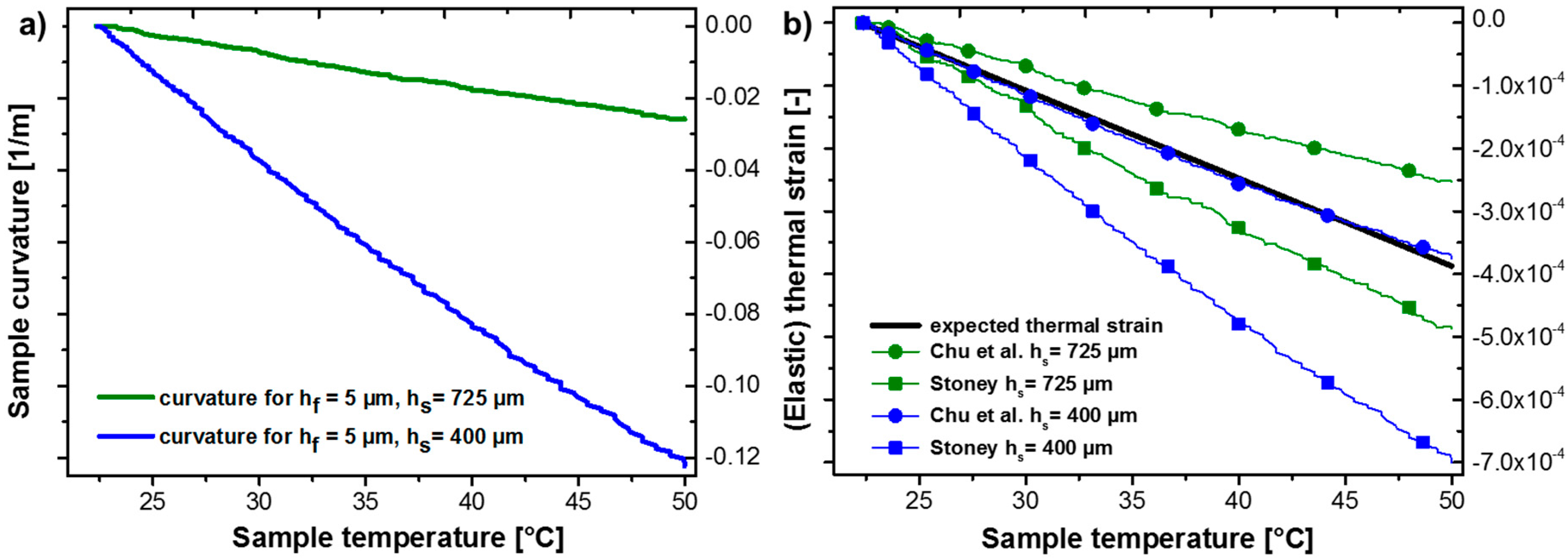
To validate the predictions of the actual bending curvature using Stoney and Chu curvature-(film) strain relations, the curvature evolution due to thermal mismatch was measured for substrate thicknesses of hs = 725 and 400 µm using substrates that were processed using semiconductor industry tools to exclude preparation artefacts. Both wafers had the same 5 µm thick Cu film on the top, and specimens of 10 × 10 mm in lateral dimension were used. In Figure 3a, the two corresponding sample curvatures are presented from room temperature up to 50 °C, where pure elastic strain development can be assumed. In both cases a linear curvature-temperature (strain) relationship was observed. The decrease of hs down to 400 µm increased the substrate curvature by a factor of ~5. For both configurations, the resulting thermal elastic strain in the copper film at any given temperature was nearly the same and followed Equation (2). We assume a constant CTE mismatch between Cu and Si of Δα = 14 ppm/K. Using the temperature data from the curvature measurements, the respective strain evolution is plotted as a thick black line in Figure 3b. It should be noted that due to the finite substrate thicknesses, a slight deviation to a smaller compressive film strain is present since a small portion of the mismatch strain is carried by the substrate. For the presented configurations this deviation can be neglected, because even for the thinner substrate the film thickness represents only about 1.25% of the total sample thickness (400 µm thick substrate, 5 µm thin film). As displayed in Table 2, a thermal strain of −3.9 × 10⁻⁴ and −65 MPa respectively (using σf = εm Mf, with Mf = 168 GPa) at 50 °C is obtained. Rearranging Equations (1) and (3), we can calculate the strain from the curvature data using Ms = 180.5 GPa. For a common wafer thickness, hs = 725 µm, final strains of −4.9 × 10⁻⁴ and −2.5 × 10⁻⁴ are obtained, which would result in −82 MPa and −42 MPa for Stoney and Chu, respectively. One could argue that this discrepancy regarding an overestimation for Stoney (and an underestimation for Chu’s relation) could simply be a sensitivity problem due to the small curvature evolution [22]. However, a clearer picture evolves for hs = 400 µm, where Stoney’s relationship would result in −7.0 × 10⁻⁴ and −118 MPa. This would overestimate the strain/stress by almost a factor of ~2, whereas the analysis of Chu et al. perfectly correlates with the developed stress by the predicted CTE mismatch of −65 MPa in the Cu film.
These observations confirm that, in general, Stoney’s equation is only an approximation of the stress development for thin films on thick rigid substrates. For thin substrates, it leads to the wrong curvature-strain relationship, while the Chu et al. derivation, where the curvature is ~2·κstoney, correlates well with our experimental observations. In fact, this emphasizes that the simplified model of having a net-zero bending moment with regard to the composite curvature is not correct. If we consider the stress fields proposed in reference [21], Equation (15) for the Cu layer, it becomes evident that a stress/strain gradient is directly proportional to the evolving curvature κ, scaling with the resulting bending curvature and the applied thermal strain εm. This is similar to the bending strain relationship for flexible electronics, where the strain in the outer fiber (e.g., metallization layer) is proportional to its bending curvature [23]. With the decrease of hs and the understanding that the curvature is underestimated by a factor of ~2, significant strain gradients could locally lead to higher stresses in the surface region and cause an accelerated microstructure evolution, as evidenced in Figure 1 and Figure 2. Furthermore, the density of geometrically necessary dislocations ρG is proportional to |κ|, which would give rise to a strain gradient in the bent lattice curvature [24].
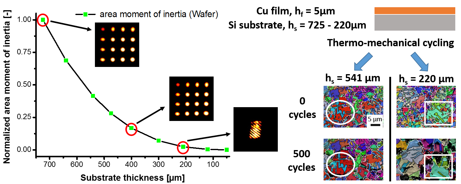
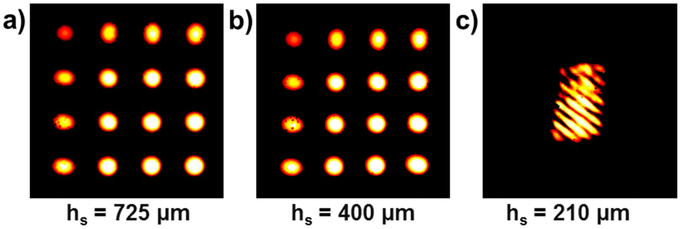
Furthermore, the CCD (charge couple device) detector images of the deflected laser beams in Figure 4 reveal that between hs = 400 µm and 210 µm, an abrupt “snap over” of the substrate curvature occurred, seen as a bifurcation of the sample curvature. Besides the impracticable measurement of the curvature evolution for hs = 210 µm, this observation points to the presence of large non-linear deformation. Focusing on the ellipsoidal shape of the detected laser spots suggests that the curvature is a function of position and that twist moments are present. Such effects rise inevitably in modern microelectronics, and are not considered in common analysis but can have a pronounced effect on the thermo-mechanical material behavior.
5. Conclusions
The detailed results regarding the microstructural evolution of 5 µm thick Cu films upon thermo-mechanical fatigue revealed a strong substrate thickness dependency. The findings showed that distinct grain growth coupled with twin migration and accelerated surface roughening was present for Cu films cycled on thin substrates with hs = 323 and 220 µm. The examination of Stoney’s curvature-strain relation using wafer curvature measurements showed distinct deviations between the expected and measured curvature. The significantly larger sample curvature in combination with expected plastic strain gradients in the film material can serve as an explanation for the accelerated material degradation. The observations with respect to non-uniform sample curvature and bifurcation for thinner substrates (e.g., 210 µm) further highlight the need for more detailed investigations of the actual limits of Stoney’s assumptions on small substrate deformation and its implications for microstructural effects on semiconductor thin film materials.
Acknowledgments
The work was performed in the project EPPL, financially supported by grants from Austria, Germany, The Netherlands, France, Italy, Portugal, and the ENIAC Joint Undertaking (ENIAC JU Grant Agreement No. 325608). This project is co-funded within the programme “Forschung, Innovation und Technologie für Informationstechnologie” by the Austrian Ministry for Transport, Innovation and Technology.
Author Contributions
Stephan Bigl, Stefan Wurster, Megan J. Cordill. and Daniel Kiener designed the experiments; Stephan Bigl generated and tested the samples with support from Stefan Wurster and Daniel Kiener; Megan J. Cordill and Daniel Kiener provided overall guidance; Stephan Bigl and Daniel Kiener wrote the manuscript. All authors discussed the results and commented on the manuscript.
Conflicts of Interest
The authors declare no conflict of interest.
References
- Stoney, G.G. The Tension of metallic films deposited by electrolysis. Proc. R. Soc. Lond. Ser. A 1909, 82, 172–175. [Google Scholar] [CrossRef]
- Timoshenko, S. Analysis of bi-metal thermostats. J. Opt. Soc. Am. 1925, 11, 233–255. [Google Scholar] [CrossRef]
- Brenner, A.; Senderoff, S. Calcuation of stress in electrodeposits from the curvature of a plated strip. J. Res. Natl. Bur. Stand 1949, 42, 105–123. [Google Scholar] [CrossRef]
- Timoshenko, S.P.; Woinowsky-Krieger, S. Theory of Plates and Shells; McGraw-Hill: New York, NY, USA, 1959. [Google Scholar]
- Saul, R.H. Effect of GaAsxP1−x transistion zone on the perfection of GaP crystals grown by deposition onto GaAs substrates. J. Appl. Phys. 1969, 40, 3273–3279. [Google Scholar] [CrossRef]
- Freund, L.B.; Floro, J.A.; Chason, E. Extensions of the Stoney Formula for substrate curvature to configurations with thin substrates or large deformations. Appl. Phys. Lett. 1999, 74, 1987–1989. [Google Scholar] [CrossRef]
- Janssen, G.; Abdalla, M.; van Keulen, F.; Pujada, B.; van Venrooy, B. Celebrating the 100th anniversary of the Stoney equation for film stress: Developments from polycrystalline steel strips to single crystal silicon wafers. Thin Solid Films 2009, 517, 1858–1867. [Google Scholar] [CrossRef]
- Vobecky, J.; Rahimo, M.; Kopta, A.; Linder, S. Exploring the Silicon Design Limits of Thin Wafer IGBT Technology: The Controlled Punch through (CPT) IGBT. In Proceedings of the 2008 20th International Symposium on Power Semiconductor Devices and IC’s, Orlando, FL, USA, 18–22 May 2008; pp. 76–79. [Google Scholar]
- Zoschke, K.; Wegner, M.; Wilke, M.; Jürgensen, N.; Lopper, C.; Kuna, I.; Glaw, V.; Röder, J.; Wünsch, O.; Wolf, M.J.; et al. Evaluation of thin wafer processing using a temporary wafer handling system as key technology for 3D system integration. In Proceedings of the 2010 Proceedings 60th Electronic Components and Technology Conference (ECTC), Las Vegas, NV, USA, 1–4 June 2010; pp. 1385–1392. [Google Scholar]
- Zhang, G.; Schwaiger, R.; Volkert, C.; Kraft, O. Effect of film thickness and grain size on fatigue-induced dislocation structures in Cu thin films. Philos. Mag. Lett. 2003, 83, 477–483. [Google Scholar] [CrossRef]
- Zhang, G.; Volkert, C.; Schwaiger, R.; Wellner, P.; Arzt, E.; Kraft, O. Length-scale-controlled fatigue mechanisms in thin copper films. Acta Mater. 2006, 54, 3127–3139. [Google Scholar] [CrossRef]
- Kraft, O.; Schwaiger, R.; Wellner, P. Fatigue in thin films: Lifetime and damage formation. Mater. Sci. Eng. A 2001, 319–321, 919–923. [Google Scholar] [CrossRef]
- Finot, M.; Blech, I.; Suresh, S.; Fujimoto, H. Large deformation and geometric instability of substructures with thin-film deposits. J. Appl. Phys. 1997, 81, 3457–3464. [Google Scholar] [CrossRef]
- Harper, B.D.; Chih-Ping, W. A geometrically nonlinear model for predicting the intrinsic film stress by the bending-plate method. Int. J. Solids Struct. 1990, 26, 511–525. [Google Scholar] [CrossRef]
- Wimmer, A.; Smolka, M.; Heinz, W.; Detzel, T.; Robl, W.; Motz, C.; Eyert, V.; Wimmer, E.; Jahnel, F.; Treichler, R.; et al. Temperature dependent transistion of intragranular plastic to intergranular brittle failure in electrodeposited Cu micro-tensile samples. Mater. Sci. Eng. A 2014, 618, 398–405. [Google Scholar] [CrossRef]
- Bigl, S.; Schöberl, T.; Wurster, S.; Cordill, M.J.; Kiener, D. Correlative microstructure and topography informed nanoindentation of copper films. Surf. Coat. Technol. 2016, 308, 404–413. [Google Scholar] [CrossRef]
- Bigl, S.; Wurster, S.; Cordill, M.J.; Kiener, D. Site specific microstructural evolution of themo-mechanically fatigued copper films. BHM Berg- und Hüttenmännische Monatshefte 2015, 160, 235–239. [Google Scholar] [CrossRef]
- Chavez, K.; Hess, D. A novel method of etching copper oxide using acetic acid. J. Electrochem. Soc. 2001, 148, G640–G643. [Google Scholar] [CrossRef]
- Bigl, S.; Wurster, S.; Cordill, M.J.; Kiener, D. Advanced characterisation of thermo-mechanical fatigue mechanisms of different copper film systems for wafer metallizations. Thin Solid Films 2016, 612, 153–164. [Google Scholar] [CrossRef]
- Bigl, S.; Heinz, W.; Kahn, M.; Schoenherr, H.; Cordill, M.J. High-temperature characterization of silicon dioxide films with wafer curvature. JOM 2015, 67, 2902–2907. [Google Scholar] [CrossRef]
- Chu, S. Elastic bending of semiconductor wafer revisited and comments on Stoney’s equation. J. Electrochem. Soc. 1998, 145, 3621–3627. [Google Scholar] [CrossRef]
- Chason, E. Resolution and Sensitivity of Stress Measurements with the k-Space Multi-Beam Optical Sensor (MOS) System; Sandia National Laboratories: San Antonio, TX, USA, 2005. [Google Scholar]
- Suo, Z.; Ma, E.; Gleskova, H.; Wagner, S. Mechanics of rollable and foldable film-on-foil electronics. Appl. Phys. Lett. 1999, 74, 1177–1179. [Google Scholar] [CrossRef]
- Fleck, N.; Hutchinson, J. Strain gradient plasticity. Adv. Appl. Mech. 1997, 33, 296–361. [Google Scholar]
Figure 1.
Microstructural evolution of 5-µm thick Cu films on silicon substrates with different thicknesses. The inverse pole figure-image quality (IPF-IQ) images display the changes with respect to the cycling stage of 0, 100, and 500 cycles. For thicker substrates, marginal microstructural changes in the grains (circular markings) were observed during thermal cycling, whereas the on thinner substrates the grains exhibited pronounced growth and twin migration (squares). Scale bar is valid for all electron back scatter diffraction (EBSD) images.
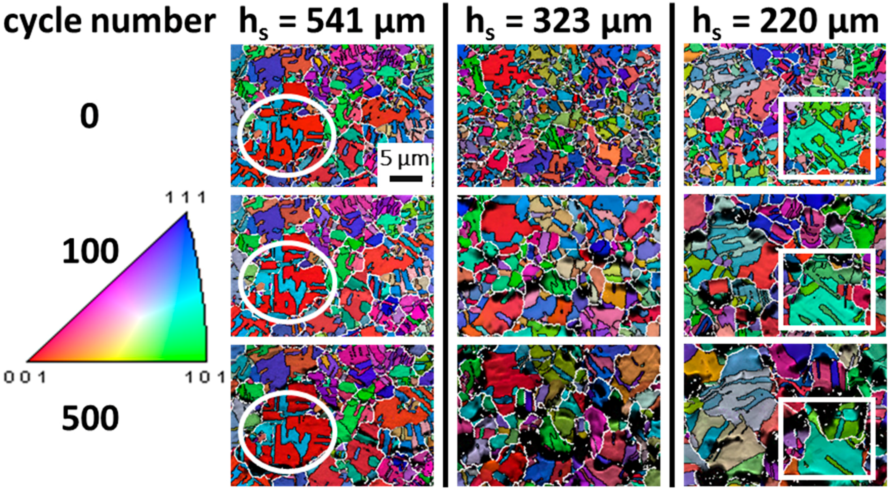
Figure 2.
(a) Root mean squared (RMS) roughness evolution of a Cu film with hf = 5 µm on silicon substrates with different thicknesses (725, 541, 323, and 220 µm) as a function of cycle number; (b) SEM micrograph and (c) Focused ion beam (FIB) cross-section of a 5 µm thick film on hs = 220 µm after 750 thermal cycles.
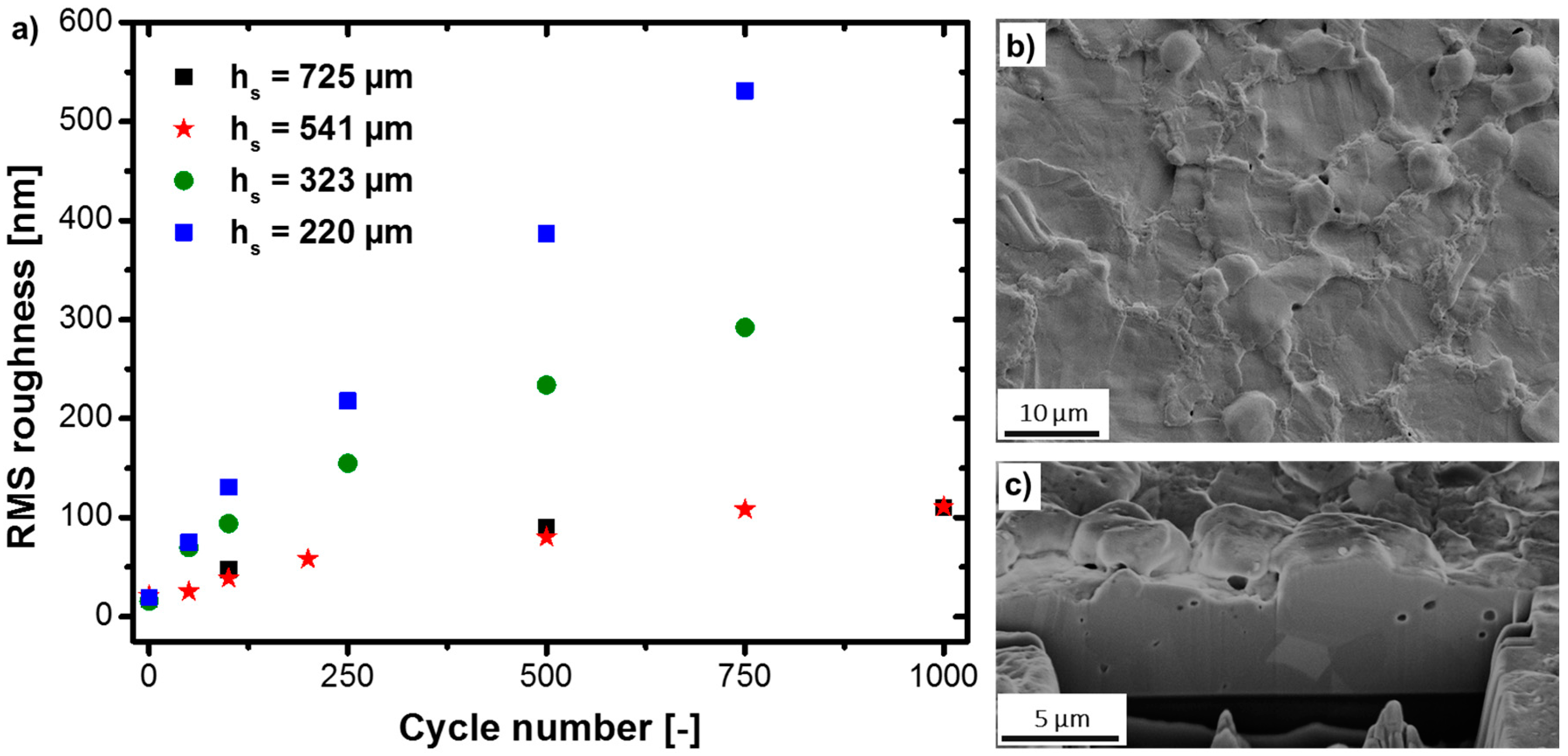
Figure 3.
(a) Curvature evolution of a Cu film with hf = 5 µm on Si with hs = 725 and 400 µm; (b) Comparison of thermal strain evolution calculated following Stoney (squares) and Chu (circles) with regard to the measured curvature.
Figure 3.
(a) Curvature evolution of a Cu film with hf = 5 µm on Si with hs = 725 and 400 µm; (b) Comparison of thermal strain evolution calculated following Stoney (squares) and Chu (circles) with regard to the measured curvature.

Figure 4.
Detected multi-laser spot grid for a Cu film with hf = 5 µm at room temperature with a varying hs of (a) 725 µm; (b) 400 µm; and (c) 210 µm.
Figure 4.
Detected multi-laser spot grid for a Cu film with hf = 5 µm at room temperature with a varying hs of (a) 725 µm; (b) 400 µm; and (c) 210 µm.


Table 1.
Grain size evolution of the Cu film with four different substrate thicknesses during cycling.
Table 1.
Grain size evolution of the Cu film with four different substrate thicknesses during cycling.
| Cycle Number (-) | Grain Size (Including Twins) (µm) | |||
|---|---|---|---|---|
| hs = 725 µm | hs = 541 µm | hs = 323 µm | hs = 220 µm | |
| 0 | 2.4 ± 0.8 | 2.3 ± 0.7 | 2.5 ± 0.7 | 2.4 ± 0.8 |
| 100 | 2.7 ± 0.9 | 2.7 ± 0.8 | 3.6 ± 1.1 | 3.8 ± 1.2 |
| 500 | 2.8 ± 0.9 | 3.0 ± 1.0 | 4.3 ± 1.3 | 5.1 ± 1.6 |
Table 2.
Comparison of the predicted strain and stress values in copper at 50 °C.
| Method of Validation | hs = 725 µm | hs = 400 µm | ||
|---|---|---|---|---|
| Compressive εm | Compressive σf | Compressive εm | Compressive σf | |
| CTE mismatch | −3.9 × 10⁻⁴ | −65 MPa | −3.9 × 10⁻⁴ | −65 MPa |
| Stoney | −4.9 × 10⁻⁴ | −82 MPa | −7.0 × 10⁻⁴ | −118 MPa |
| Chu | −2.5 × 10⁻⁴ | −42 MPa | −3.7 × 10⁻⁴ | −63 MPa |
© 2017 by the authors. Licensee MDPI, Basel, Switzerland. This article is an open access article distributed under the terms and conditions of the Creative Commons Attribution (CC BY) license (http://creativecommons.org/licenses/by/4.0/).
Share and Cite
MDPI and ACS Style
Bigl, S.; Wurster, S.; Cordill, M.J.; Kiener, D. Substrate-Influenced Thermo-Mechanical Fatigue of Copper Metallizations: Limits of Stoney’s Equation. Materials 2017, 10, 1287. https://doi.org/10.3390/ma10111287
AMA Style
Bigl S, Wurster S, Cordill MJ, Kiener D. Substrate-Influenced Thermo-Mechanical Fatigue of Copper Metallizations: Limits of Stoney’s Equation. Materials. 2017; 10(11):1287. https://doi.org/10.3390/ma10111287
Chicago/Turabian StyleBigl, Stephan, Stefan Wurster, Megan J. Cordill, and Daniel Kiener. 2017. "Substrate-Influenced Thermo-Mechanical Fatigue of Copper Metallizations: Limits of Stoney’s Equation" Materials 10, no. 11: 1287. https://doi.org/10.3390/ma10111287
Note that from the first issue of 2016, this journal uses article numbers instead of page numbers. See further details here.