1. Introduction
As the demand for renewable energy increases, alternative and sustainable transportation methods become more attractive in comparison to conventional transportation. Electric vehicles (EVs) are efficient solution which draws interest of government, manufacturers and researchers [
1,
2,
3,
4]. However, the lack of a convenient charging options prevents widespread use of EVs. In order to overcome this issue and make EVs more competitive, an efficient and reliable, high power density, low cost, small size and lightweight on-board charger for EVs becomes a valuable topic [
5].
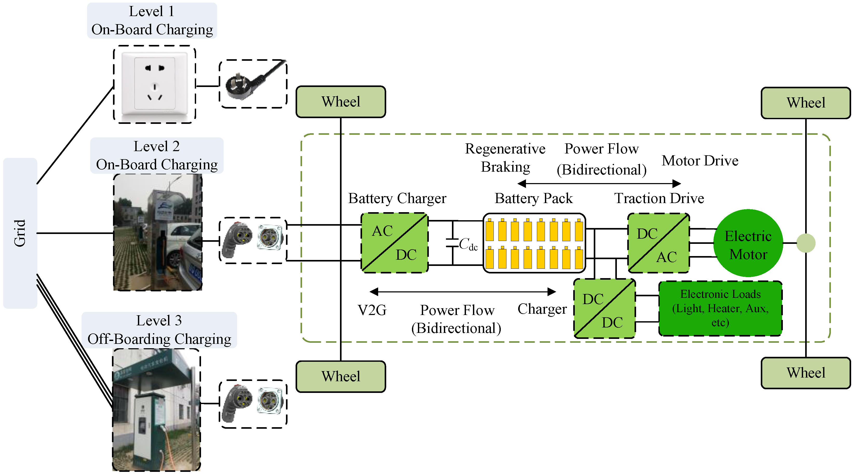
EV charging power levels defined by society of automotive engineers (SAE) are summarized and classified in
Figure 1: Level 1 charging is slow charging; Level 2 charging is assumed primary charging level; and Level 3 is intended for off-board charging infrastructure providing quick charging. In terms of application, an off-board charger can be designed for high charging rates and is less constrained by size and weight. On-board battery chargers can reduce user range anxiety by allowing for battery packs to be charged from any available power outlet [
6]. However, on-board charging increases system volume and weight. A compact, high power density charger is needed to maintain vehicle operation efficiency. Galvanic isolation from the utility grid is a favorable option in the charger circuits because of safety reasons, but isolated on-board chargers are usually avoided due to their cost impact on the system. With a dedicated socket-outlet, earth current monitoring is an optional function as mentioned in the standard [
7]. The electrical continuity of the earth conductor should be permanently monitored by the charger, and in the case of loss of electrical continuity of the earth conductor, the charger shall be switched off. In addition, if the traction battery is bonded to the vehicle chassis, the charging system shall provide a galvanic isolation between the mains and the battery. For the chargers, they are classified into conductive charging and inductive charging [
8]. The inductive charging can be implemented wireless charging, which has lower efficiency.
An on-board battery charger is an inevitable part of an EV powertrain [
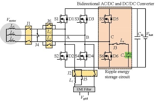
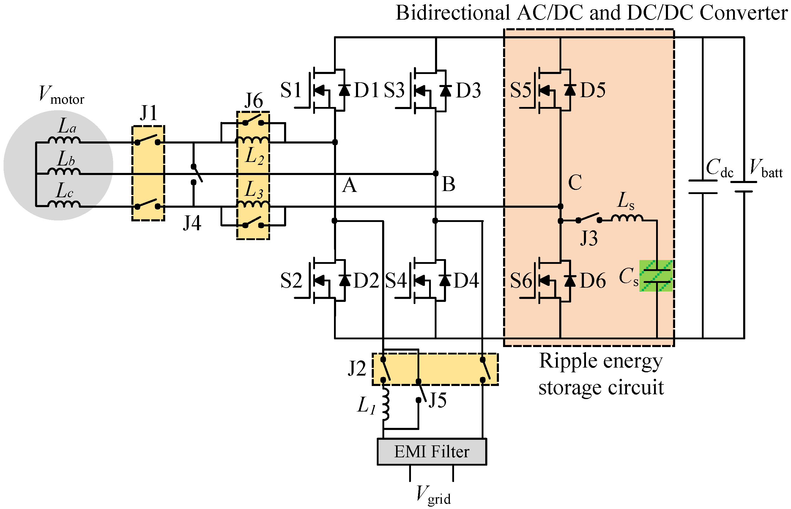
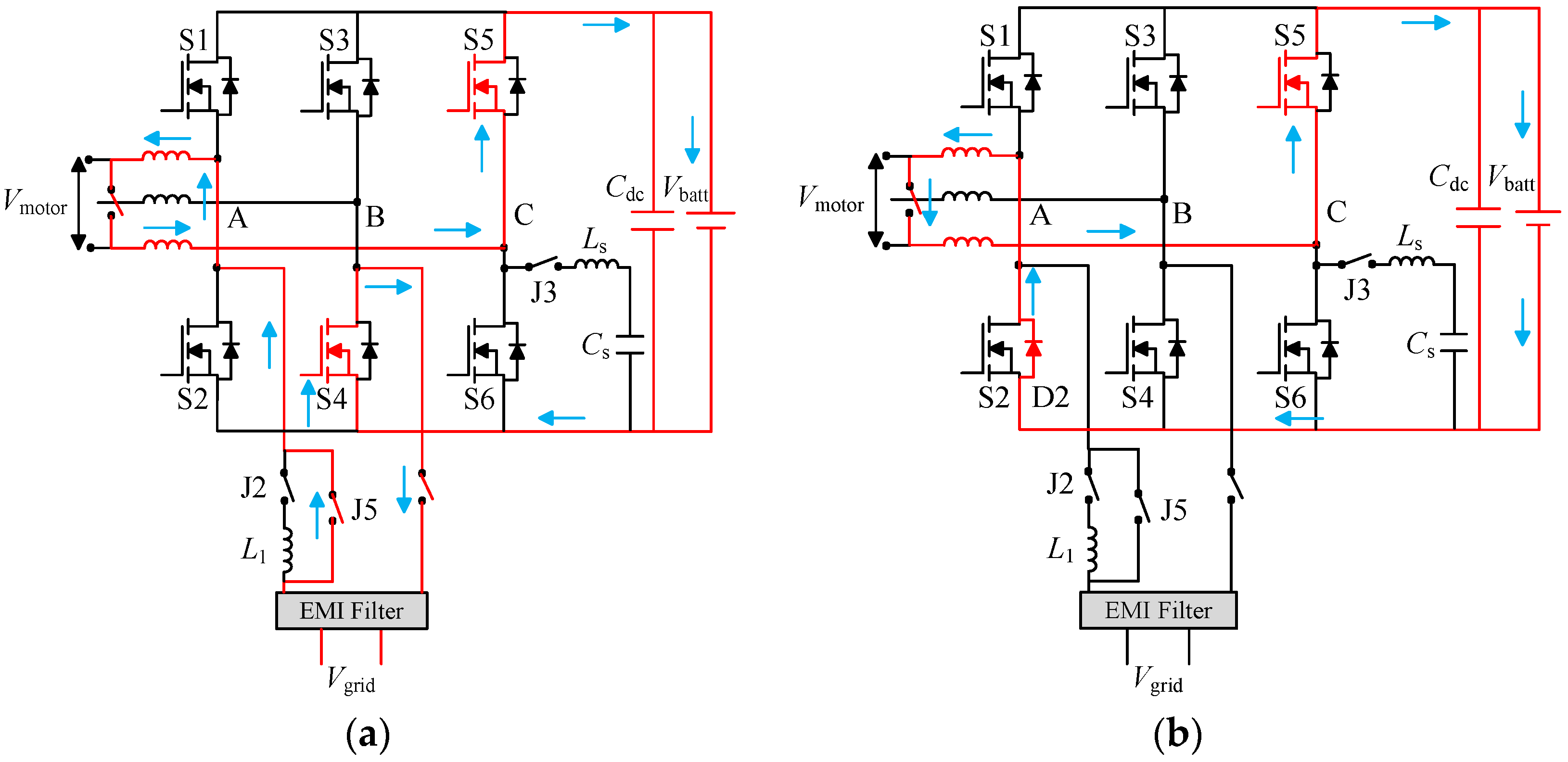
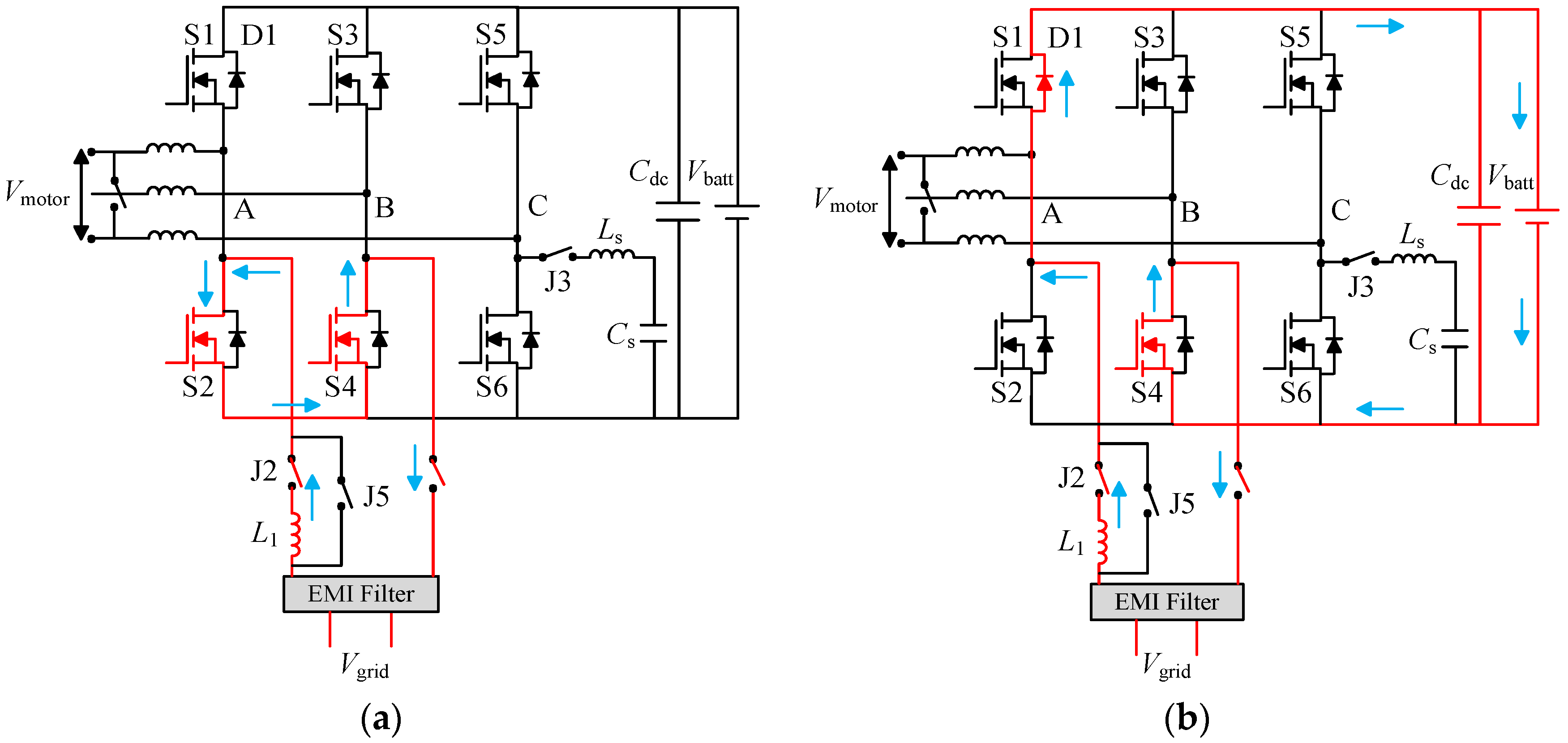
9]. From the perspective of power electronics, the on-board charger for an EV consists of an AC/DC power converter and some filter components. An efficient solution to make a high power density system is integrating the charger unit with motor drive converter. In the case of using an integrated charger, as illustrated in
Figure 2, it is viable to share the same power switching devices and passive components because motor drive mode and battery-charging mode do not happen at the same time [
10]. This configuration can effectively reduce the size and cost of the overall system. Meanwhile, with the DC/DC buck/boost charging capability, it enables operating with a wide charging range. In addition, essential capabilities such as buck for the battery voltage in motor drive mode and boost for the battery voltage in regenerative braking mode can be achieved as well [
11]. Consequently, the conventional configuration consists of at least two individual converters for two independent operation modes.
In order to obtain a simple and low cost design, transformer-less topology is used in the proposed integrated charger [
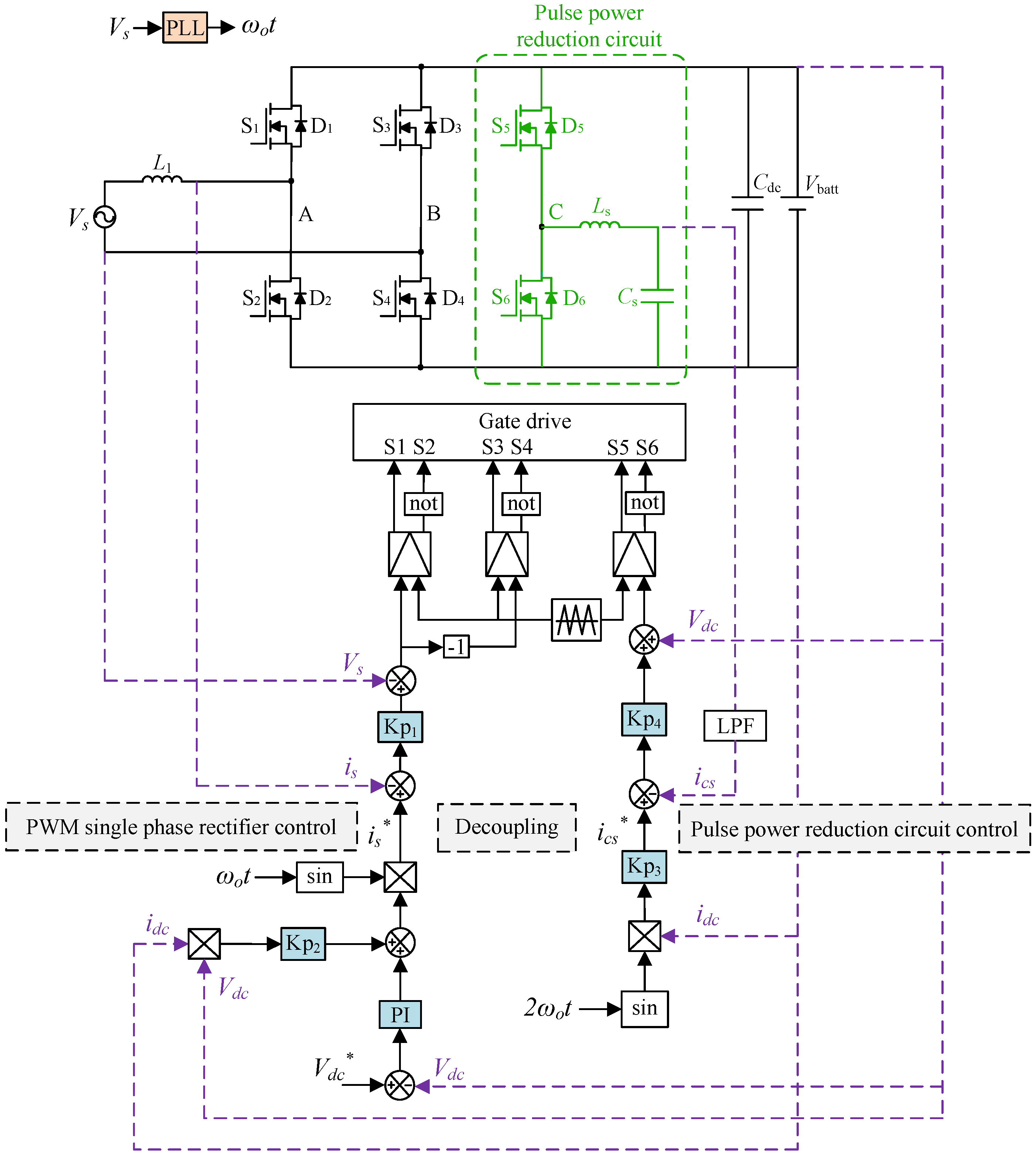
12]. Compared with traditional design, which has a transformer at the AC grid side, the transformer-less topology will improve the efficiency, reduce the total weight and allow for less complicated control. In this paper, an integrated bidirectional AC/DC and DC/DC converter is proposed to implement the integration of EV with a household electric system. The system configuration and five operational modes principles are illustrated and the pulsating power reduction circuit is presented. The control schemes are described and compared for the battery-charging mode in order to achieve a better performance.
This paper is organized as follows:
Section 2 introduces the proposed topology and explains the modes of operation in details. The utilized control schemes are illustrated in
Section 3. The simulation and experimental results are presented in
Section 4. In addition, power loss, system efficiency and thermal stress calculation results are presented in this section. Finally,
Section 5 summarizes the study based on the achieved results.
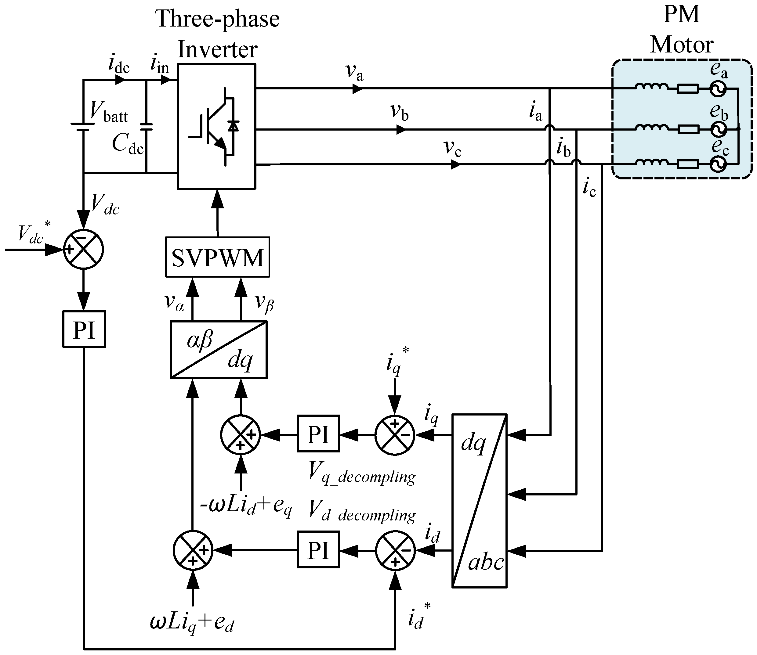
4. Simulation Results
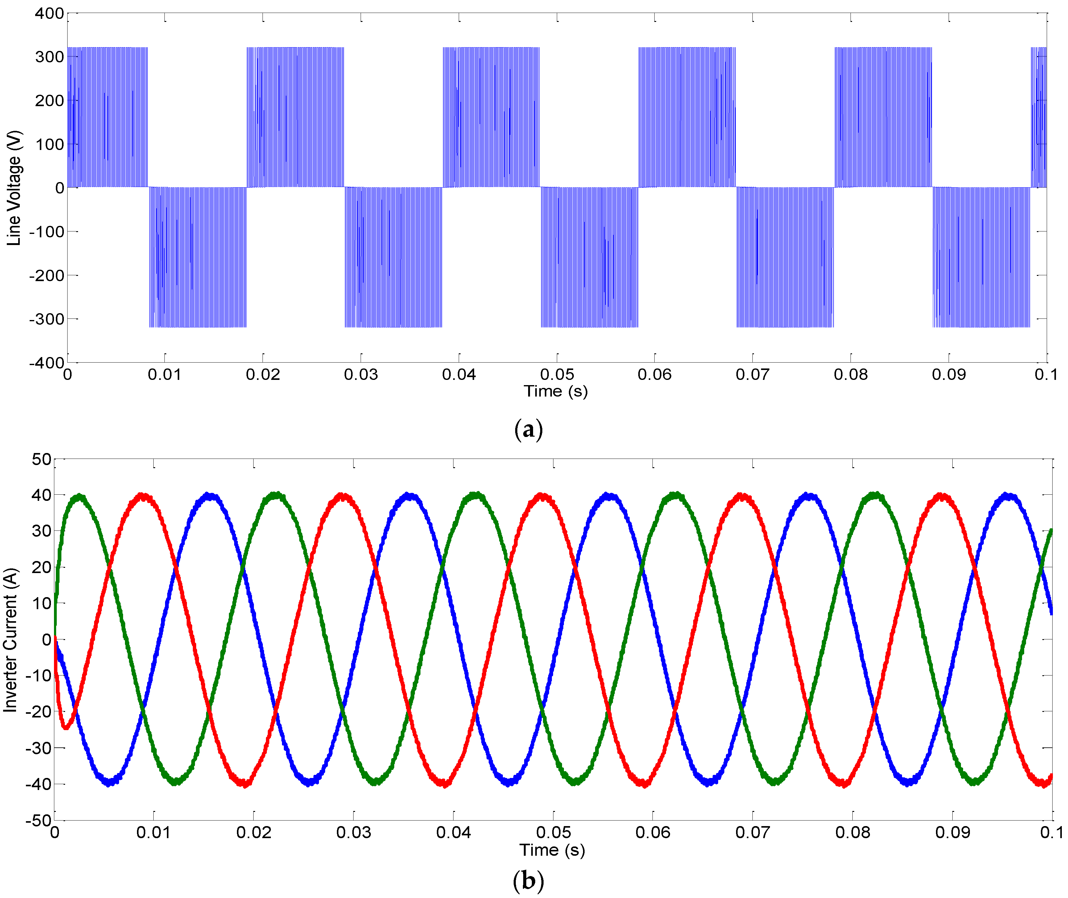
Space vector pulse width modulation (SVPWM) is acquired to conduct on the permanent magnet synchronous motor drive control. The motor drive mode performance is shown in
Figure 16.
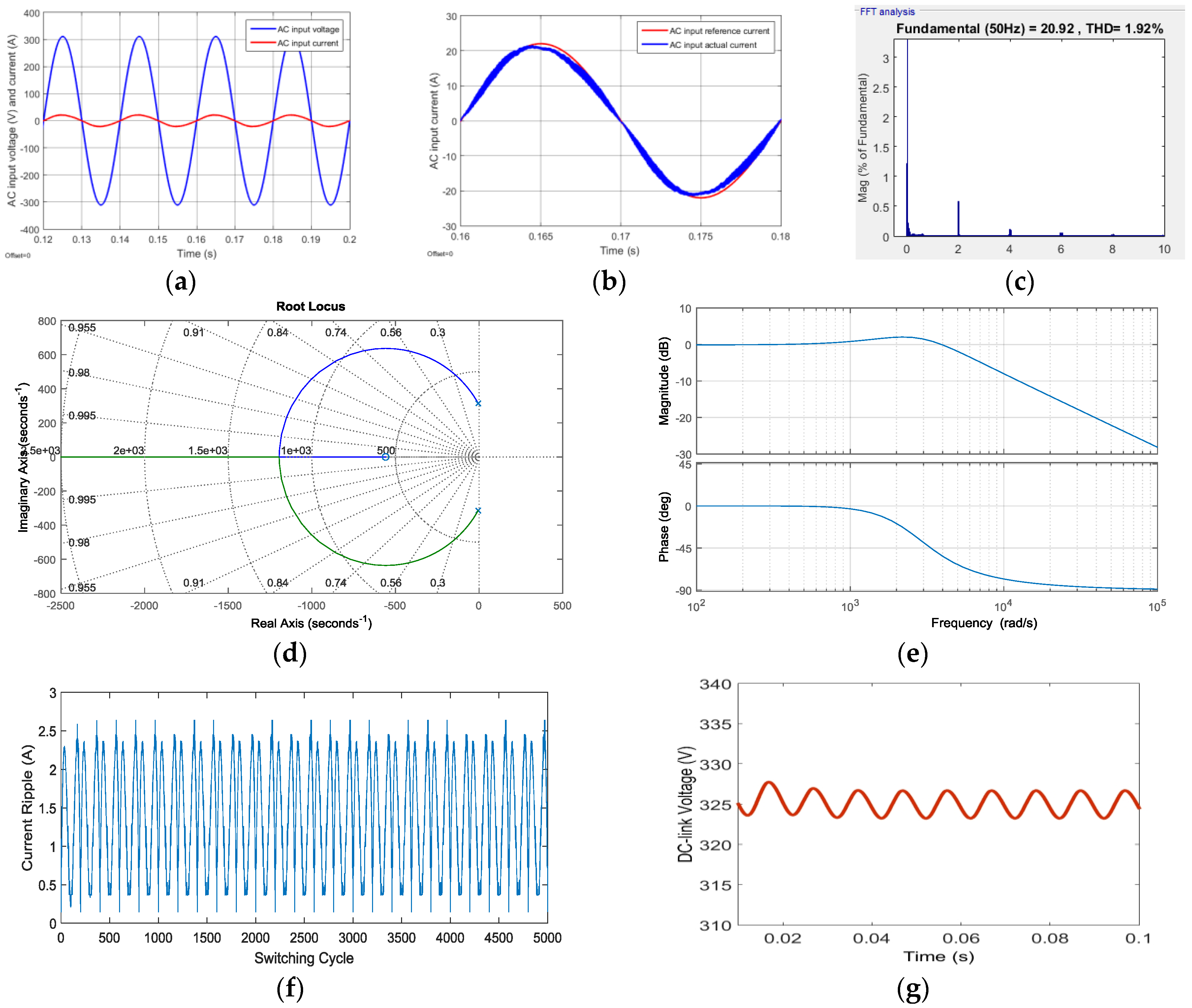
To evaluate the performance of the proposed integrated charger, AC battery-charging mode simulation has been performed. The input inductance is selected as 3 mH. To leave some margin, the root-mean-square (RMS) ripple current is 2.65 A, which is 10% of the peak output current (23.57 A). In order to show the advantage of the proposed auxiliary circuit method, simulation with ripple compensation circuit is carried out. The simulation results are shown in
Figure 17.
Simulations are carried out for AC battery-charging mode of the proposed integrated charger with the parameters shown in
Table 2. As mentioned in the previous section, the auxiliary capacitor
Cs is selected as 298 µF. The auxiliary inductor
Ls is selected as 50 µH. The DC bus capacitor is selected as 50 µF. By using MATLAB/Simulink as a simulation tool, the ripple energy from the ac side of the single-phase rectifier is verified to store in the auxiliary capacitor
Cs effectively. Using the conventional method, a 4.665 mF capacitance is selected to meet the DC bus voltage ripple within 2% limit requirement.
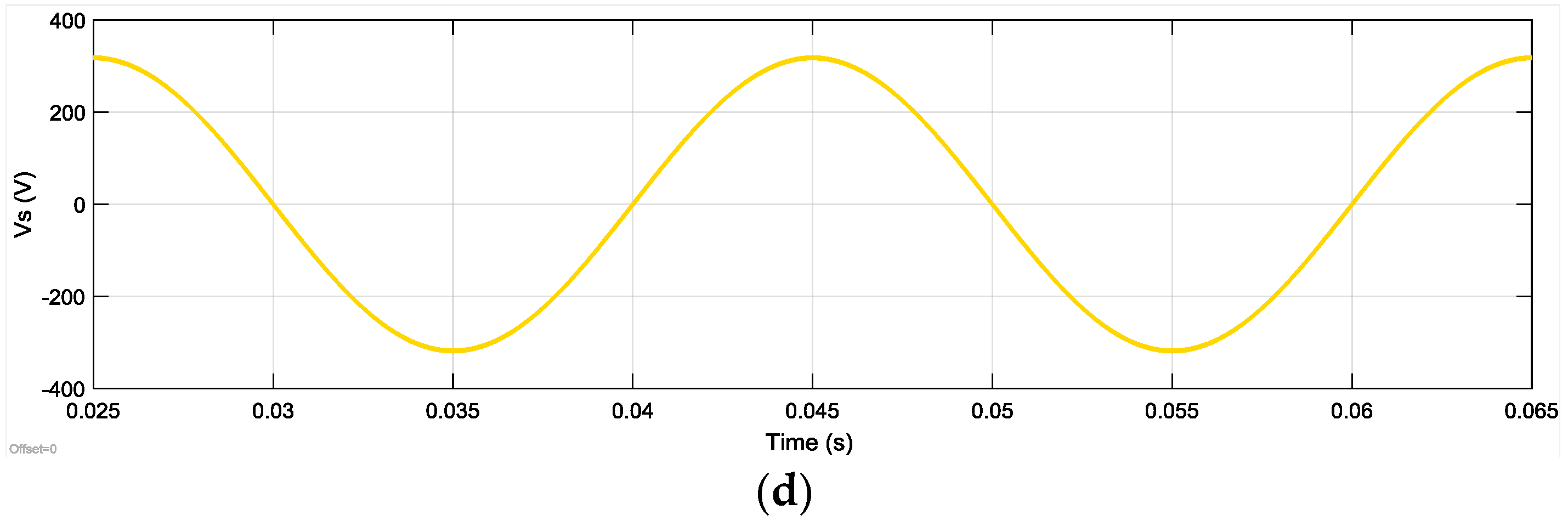
Figure 17a,b shows the AC input voltage and current, respectively. It should be noted the input current can track the reference value accurately. The total harmonic distortion is 1.92%, as shown in
Figure 17c. The root locus of rectifier is given in
Figure 17d. The root locus indicates the stability of system. The rectifier Bode plot is shown in
Figure 17e. The large crossover frequency indicates the high frequency harmonic can be filtered at switching frequency. The maximum AC input current ripple is given in
Figure 17f. It shows the maximum ripple is in accordance with unipolar modulation theoretical value. The DC-link output voltage is showed in
Figure 17g.
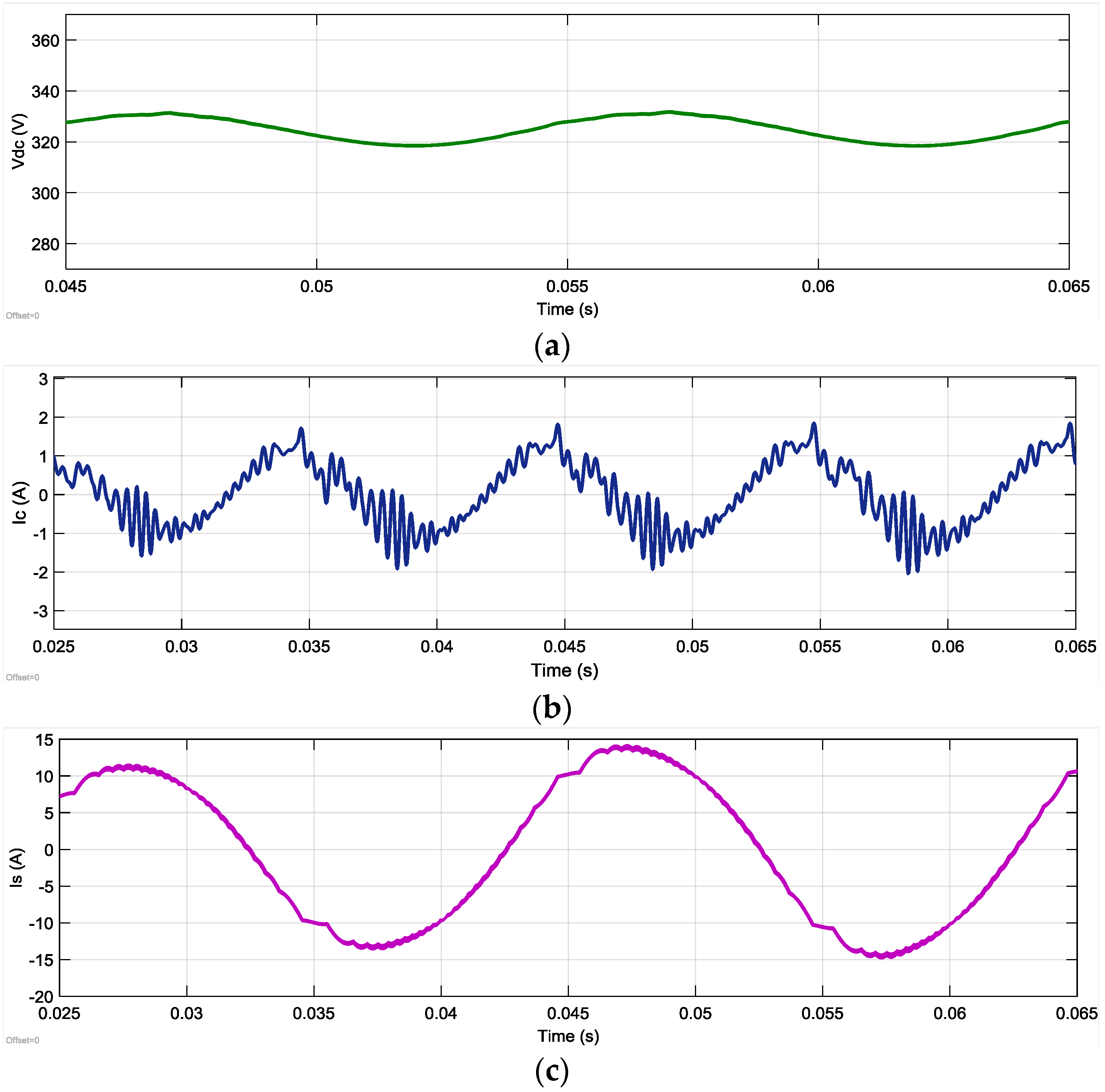
The simulation waveforms of AC battery-charging mode with active ripple energy storage circuit are presented in
Figure 18. Charging power is selected to be compatible with SAE standard J1772 level 2 charging rate [
22]. The method based on one digital signal control leads the auxiliary inductor work in continuous current mode. In addition, it provides a simple and comparatively low cost solution to implement integrated charger. The battery voltage waveform, auxiliary capacitor current, and grid side current are grid side voltage are presented in
Figure 18.
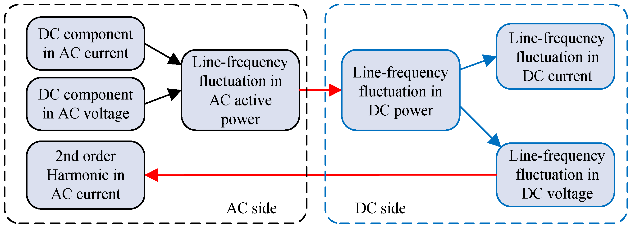
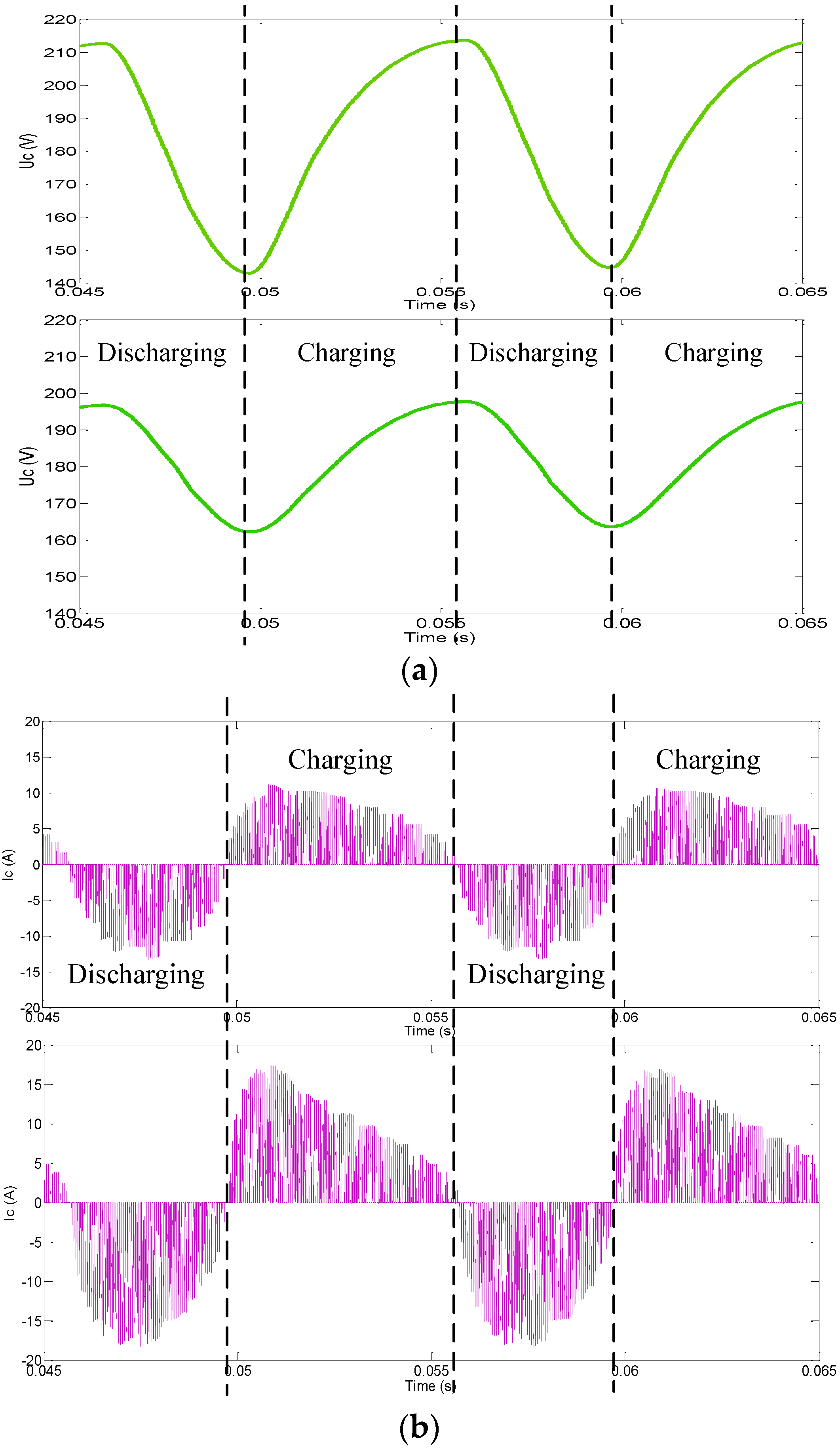
When the third leg is engaged, the 2ω
0 pulsation power is absorbed by the auxiliary circuit. The ripple energy is stored in the auxiliary capacitor. The auxiliary inductor works as a ripple energy transfer component. The proposed control scheme successfully reduces the low frequency ripple energy back to the DC bus. The compensate circuit draws the low frequency current, the current flowing into the main dc capacitor contains high frequency component. Therefore, a small DC bus capacitor is still needed to maintain a smooth DC bus voltage.
Figure 18b shows the auxiliary capacitor current. Significant 2ω
0 ripple can be observed. In
Figure 18c,d, the AC side voltage and current are illustrated. And the AC side current
Is contains some distortion due to the input inductor.
High switching frequency can improve the active ripple energy storage circuit performance effectively. The results of the integrated converter simulations at 20 kHz are shown in the upper side of
Figure 19, while the results of the integrated charger simulations at 73 kHz shown in the lower half of the
Figure 19. As observed in
Figure 19, by increasing switching frequency, the auxiliary inductance is selected as 30 µH in the system with the 73 kHz switching frequency. However, this will lead to a high current harmonic in auxiliary capacitor.
According to the comparison, there is a trade-off between one PWM signal control strategy and two PWM signals control strategy for auxiliary circuit. For the S5 and S6 control separately, it can achieve DCM, keeping the value of ripple energy transfer inductance at the minimum. In addition, its control scheme is more complex than one PWM signal control.
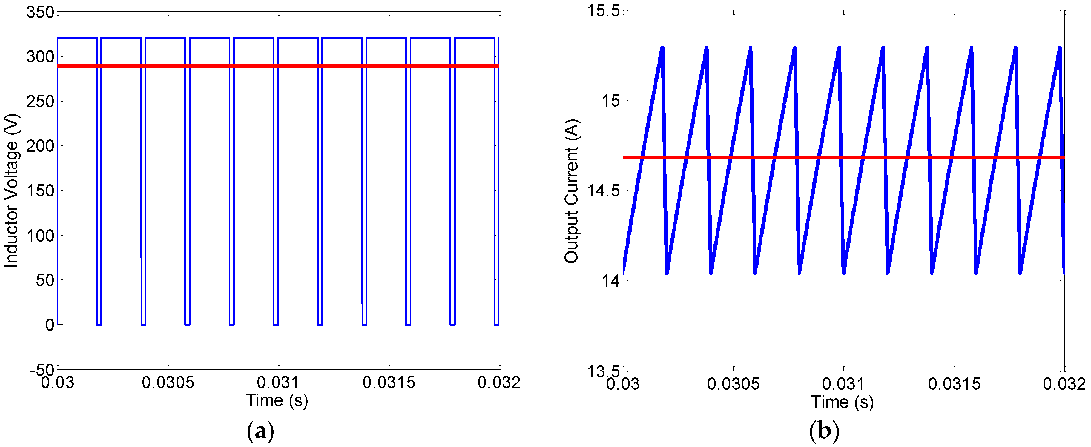
The steady states of DC/DC buck operation have also been simulated. The results for the DC external power source voltage of 400 V and the integrated charger is considered able to operate as a DC/DC buck converter, are shown in
Figure 20. The inductor voltage and output current are shown in
Figure 20, respectively. It is seen that the DC/DC buck operation can work properly.
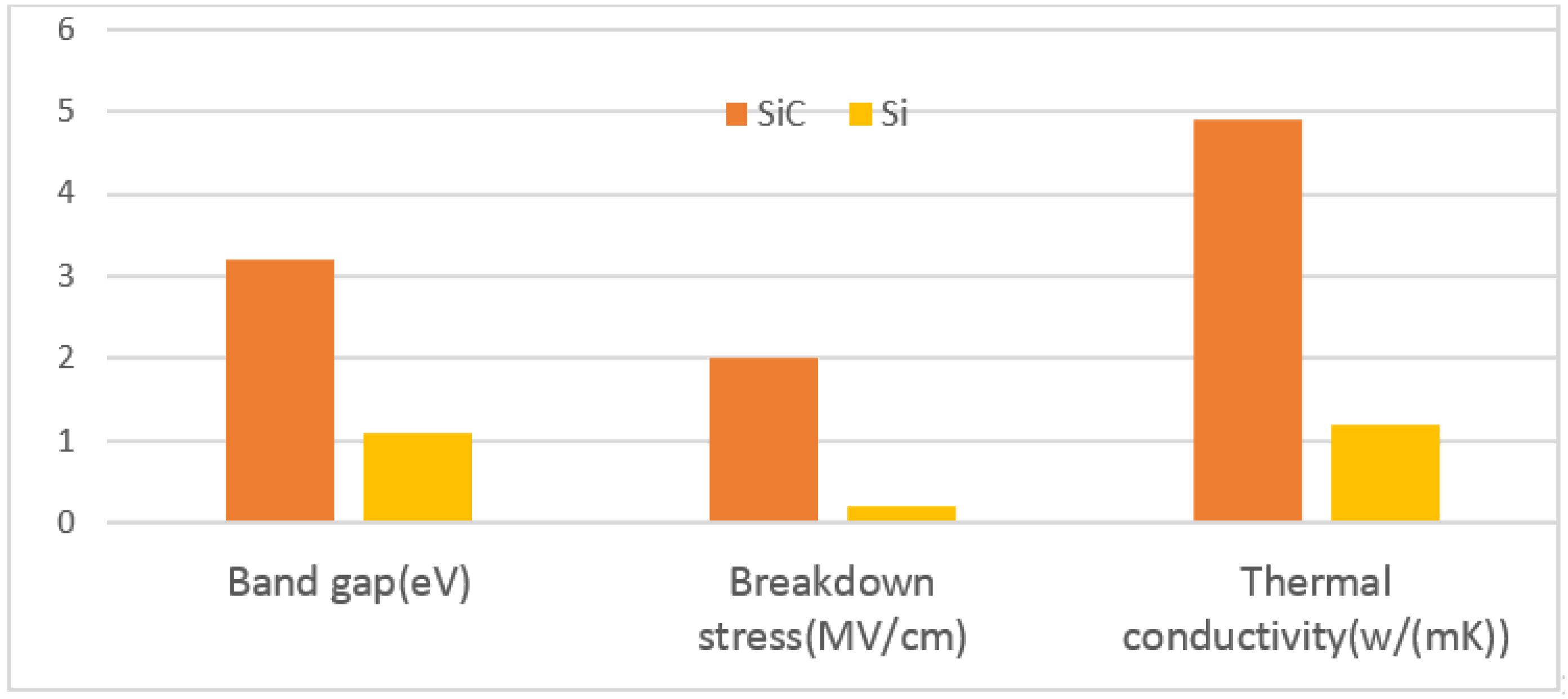
In this paper, two types of power devices are compared, i.e., silicon (Si) IGBT module and silicon carbide (SiC) MOSFET module. The state-of-the-art power devices are investigated for the integrated charger application. Wide-bandgap SiC material meet the demand for novel power semiconductor devices capable of operating at higher voltage, higher frequency and higher temperature. The comparison between Si and SiC material properties is shown in
Figure 21. This section will develop the analytical averaged loss model for the power devices shown in
Figure 2. The power loss and the efficiency variation with switching frequency of Si IGBT module and SiC MOSTFE module will also be investigated. Device characteristics are extracted from module datasheet.
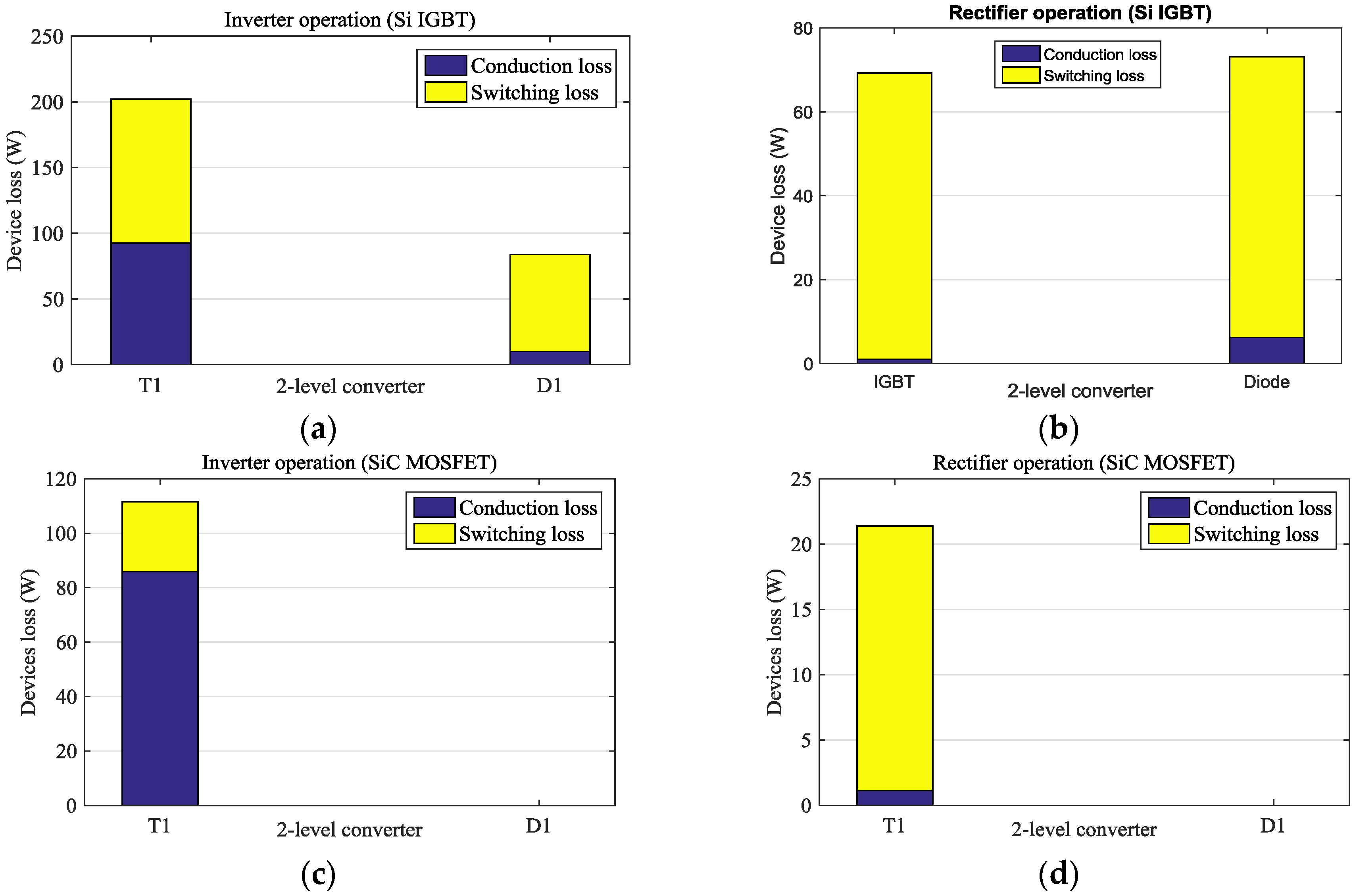
The switching device power loss can be characterized by the forward voltage drop during conduction and the turn-on and turn-off energy during switching. For simplification, the conduction characteristic of the devices is considered to be linear, which means on-state resistance is assumed as a fixed value. Due to the bidirectional current conductivity of the MOSFET channel, an assumption is made to simplify the calculation that MOSFET conduct all the load current throughout the period. In fact, the Schottky diode and the body diode share a part of the load current as well when the load current is negative. Based on above assumption, the conduction loss only occur in MOSFET. For Si IGBT and SiC MOSFET, the switching loss includes turn-on and turn-off losses. For diode, the switching loss only includes turn-off loss dissipated in the reverse recovery process. MOSFET is assumed to conduct all the load current during the negative current interval, but the switching loss still occur in the Schottky diode. Due to the existence of dead-time, load current flow to the Schottky diode, and then flow to the MOSFET. For SiC MOSFET manufacturers, it is claimed zero reverse recovery current, which means no reverse recovery loss for SiC module. The total loss is the sum of conduction loss and switching loss in all power devices. The devices used for comparison are Si IGBT module from SKM300GA12V (1200 V, 300 A, Semikron, Nuremberg, Germany) and SiC MOSFET module from CAS300M12BM2 (1200 V, 300 A, Cree, Durham, NC, USA).
Figure 22 shows the loss distribution among the devices for rectifier and inverter operation with a modulation index of 0.9 and unity power factor. The full list of Si-based IGBT losses and SiC-based MOSFET losses are given in the
appendix.
Figure 22a,b illustrates the power loss distribution in integrated converter applying inverter operation and rectifier operation, respectively. As shown in
Figure 22a, the switching loss dominate 60% total power loss occur in Si IGBT. As shown in
Figure 22c,d, it is assumed that all power loss occur only in MOSFET. It illustrates that SiC MOSFET have a good performance in reducing switching loss. The efficiency of Si-based module drop fast compared to SiC-based module with the switching frequency variation.
Figure 22e,f shows the SiC MOSFET excellent performance and attractive potential in the applications of high switching frequency. At frequency above 20 kHz, the switching loss contribute to a significant amount of power dissipation [
23]. The results for both Si and SiC converter volume breakdown are shown in
Figure 22g,h. It should be noted that the switching frequency is 73 kHz for SiC converter and 20 kHz for Si converter. As can be seen, the inductor volume is reduced by approximately 31%. As expected, the volume of the converter decreases with switching frequency variation due to the good performance of SiC.
The junction temperature describes the temperature inside the chip, which is relevant for the loss and safe operating area. The power pulsation may cause extra thermal stress to the single-phase PWM power device and auxiliary circuit power device. In order to evaluate the thermal performance of the integrated converter, the power device junction temperature variation are simulated.
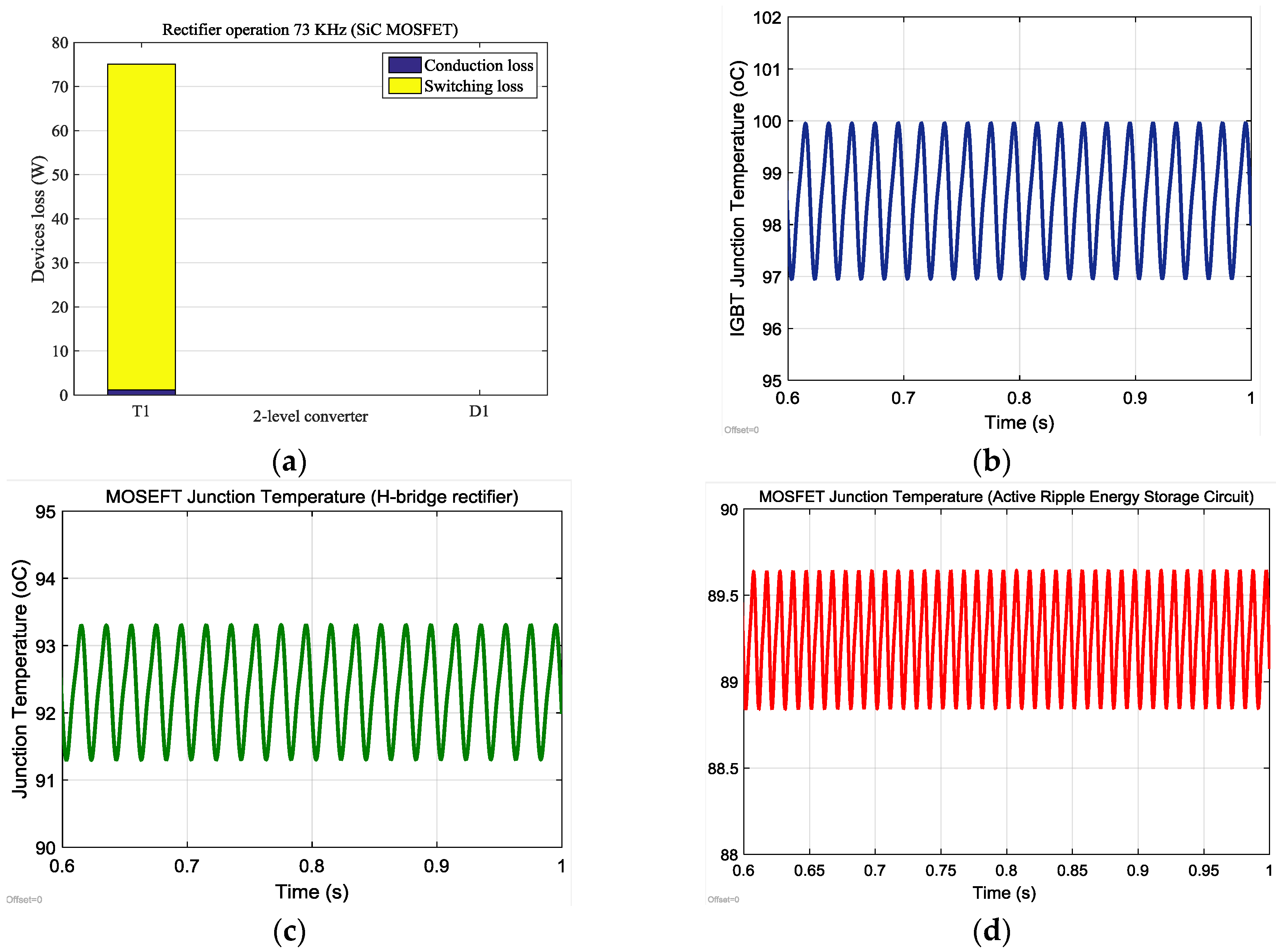
Figure 23a shows H-bridge rectifier device power loss at 73 kHz, which indicates at frequency above 20 kHz, the switching loss contributes to a significant amount of power dissipation.
Figure 23b–d shows the H-bridge and ripple energy reduction circuit device junction temperature variation. The Foster thermal network is used to calculate the junction temperature variation. The heatsink temperature is assumed to be fixed at 80 °C due to its large thermal time constant [
24]. For the H-bridge, the IGBT temperature varies between 97 and 100 °C. When SiC MOSFET is used in single-phase, the MOSFET temperature various between 91.3 and 93.3 °C. When the auxiliary compensation circuit is applied, the MOSFET temperature varies between 88.8 and 89.7 °C. The larger junction temperature variation may reduce the lifetime of the power device. The thermal design should ensure the peak temperature is lower than the maximum allowance junction temperature.
High power density is one of the key motivations for the integration of power electronics components. Integrated converters are designed not only to meet the requirement of input and output, but also to achieve a light weight and a small size. The auxiliary ripple energy reduction circuit can also achieve a high power density, as discussed above.
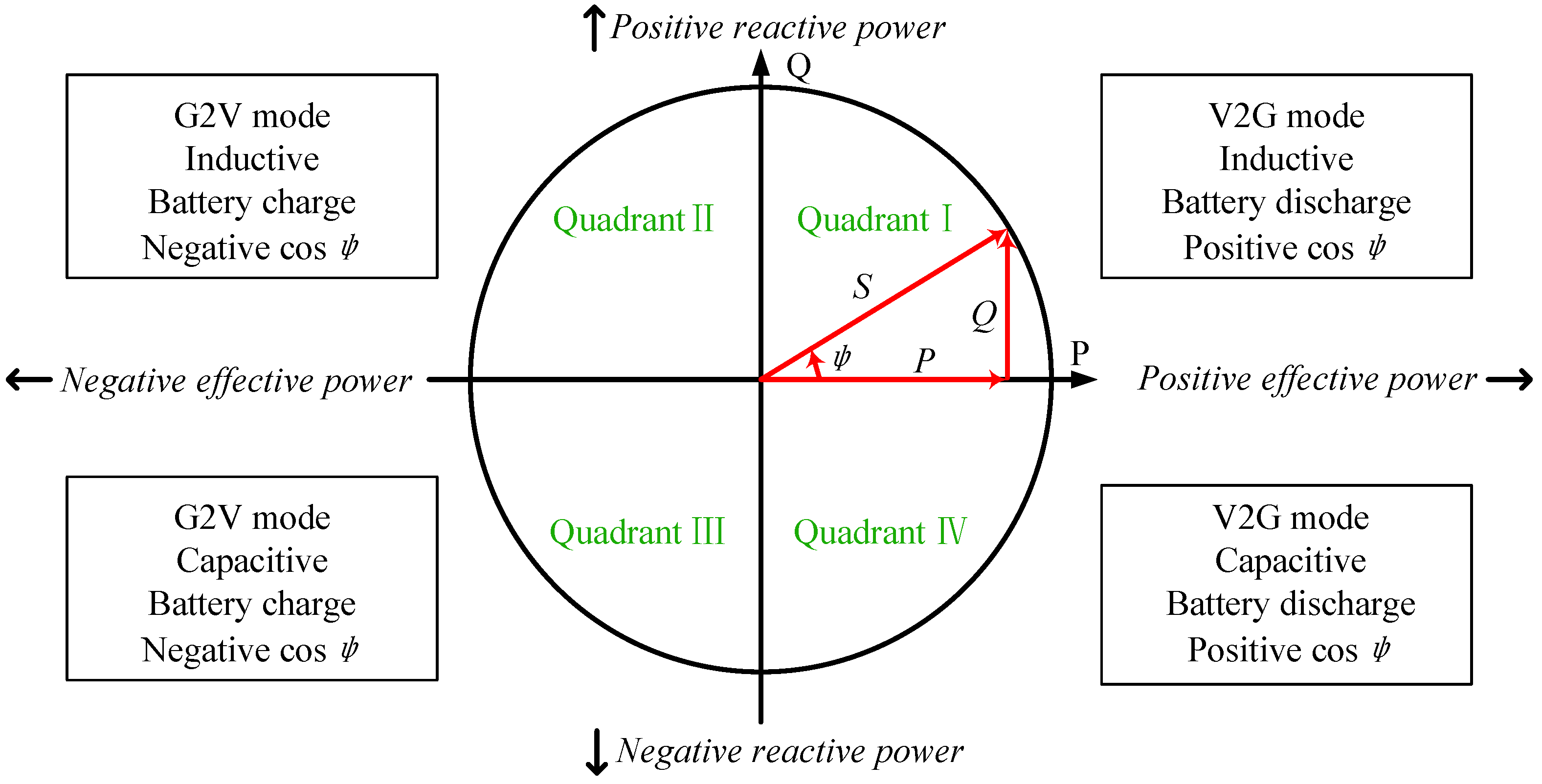
In order to verify the effectiveness of the proposed system, an integrated multifunctional bidirectional AC/DC and DC/DC converter for electric vehicles has been implemented. The propulsion and AC/DC charging performances of the proposed topology and control schemes are verified in this paper.
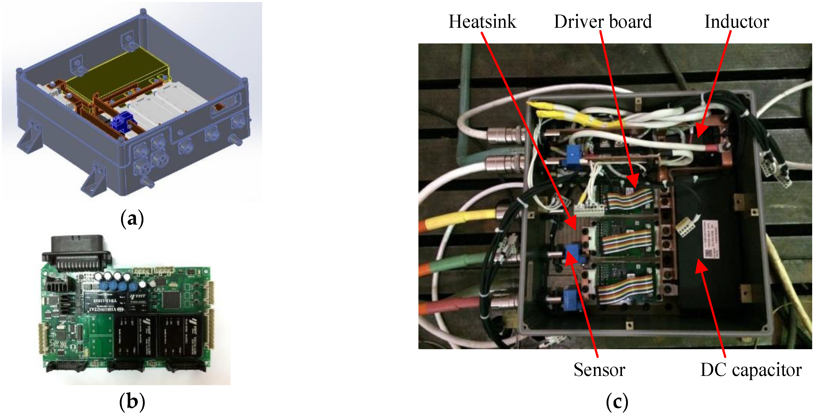
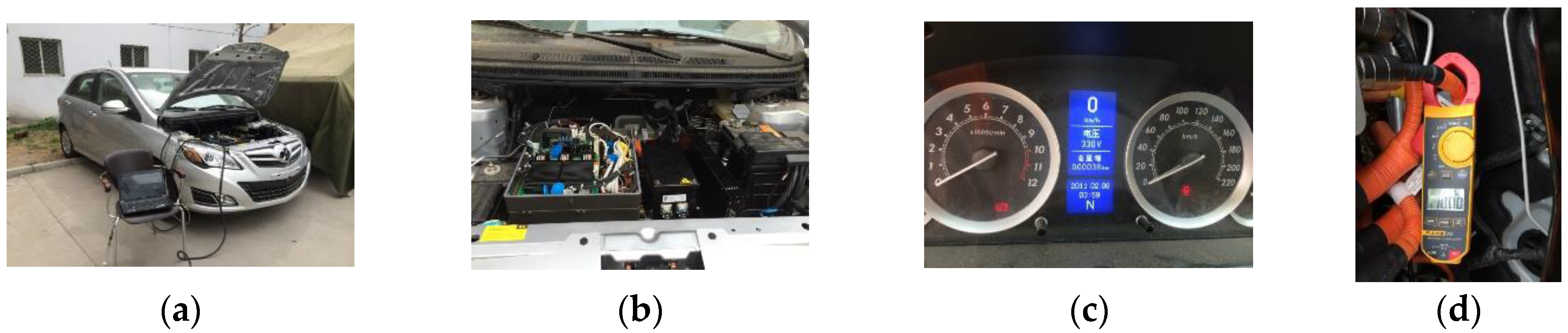
Figure 24a illustrates the system layout design. As mentioned earlier, power module, heatsink, controller, drive board, input inductor, DC capacitor and sensors are selected in the integrated converter. The controller is shown in
Figure 24b. The photo of the experimental hardware prototype platform is shown in
Figure 24c. The power module in the main power circuit is SEMIKRON SKM300GA12V with the maximum junction temperature 175 °C.
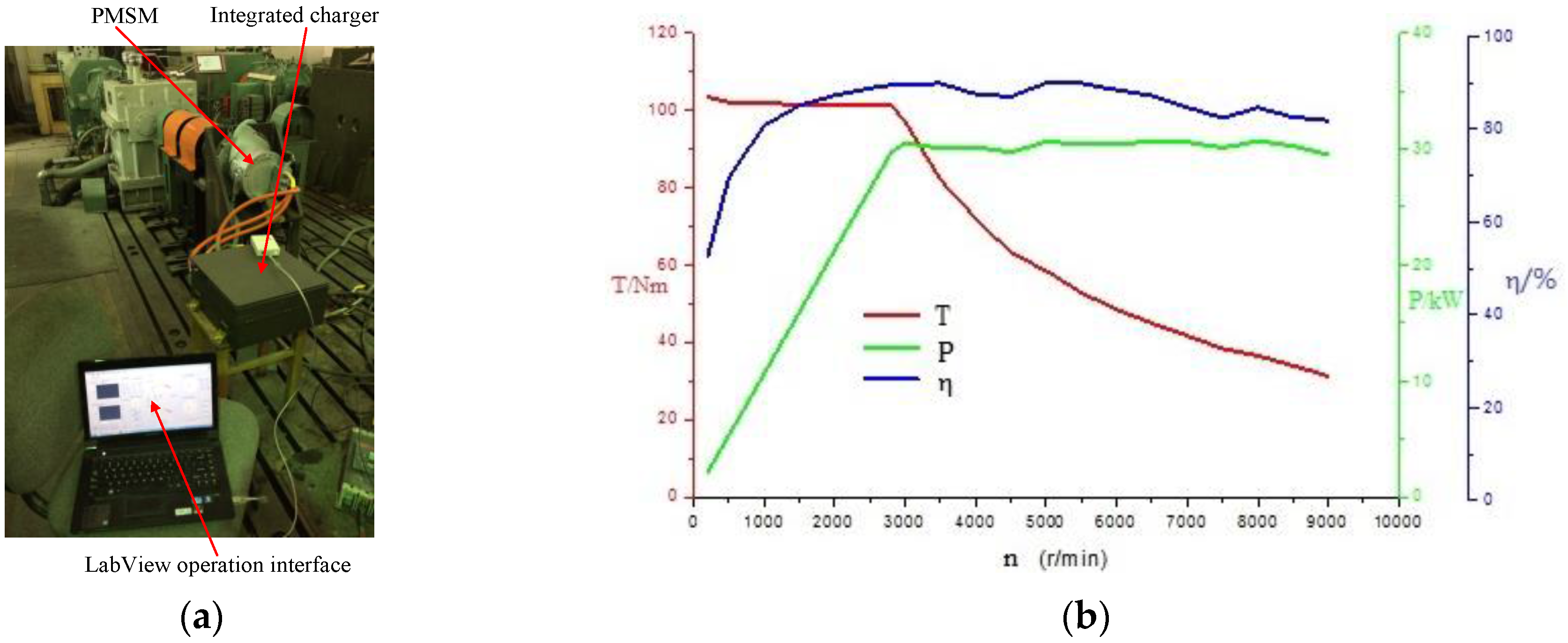
The motor driving operation photo of experimental prototype platform is shown in
Figure 25a. The drive control method is implemented, as shown in
Figure 25b.
Figure 25b shows the rated speed is 3000 rpm, the rated torque is 100 Nm and the rated power is controlled as 30 kW, which are the same as the theoretical values.
Figure 26a,b shows AC/DC battery-charging operation experimental setup and results of the DC-link voltage and current.
Figure 26c,d shows the DC-link voltage is 330 V and the load current is 10 A, respectively. Thus, the proposed charging control strategy can retain 3.3 kW charging power.
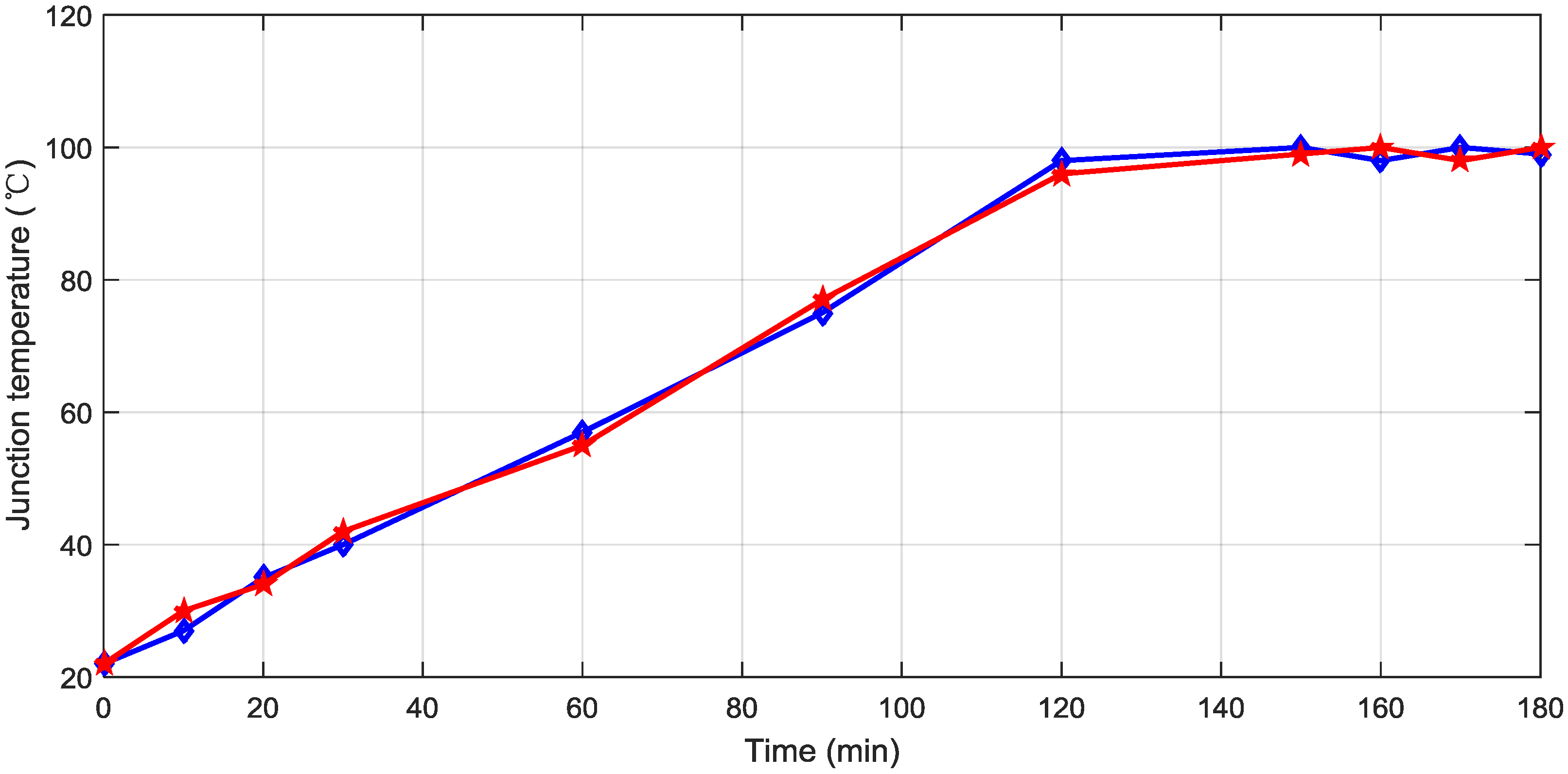
Figure 27 shows the rectifier device junction temperature variation. With AC/DC battery charging operation, the Si IGBT maximum junction temperature varies between 98 and 100 °C. The larger junction temperature variation may reduce the lifetime of the power device. The thermal design should also make sure the peak temperature does not exceed the maximum allowable junction temperature, 175 °C.


