Article

Mitigation Emission Strategy Based on Resonances from a Power Inverter System in Electric Vehicles

1
National Engineering Laboratory for Electric Vehicle, Beijing Institute of Technology, Beijing 100081, China
2
Co-Innovation Center of Electric Vehicles in Beijing, Beijing Institute of Technology, Beijing 100081, China
3
Electromagnetic Compatibility Laboratory, Missouri University of Science and Technology, Rolla, MO 65409, USA
4
John Deere Electronic Solutions, Fargo, ND 58102, USA
*
Author to whom correspondence should be addressed.
These authors contributed equally to this work.
Energies 2016, 9(6), 419; https://doi.org/10.3390/en9060419
Submission received: 24 December 2015 / Revised: 14 May 2016 / Accepted: 23 May 2016 / Published: 31 May 2016
(This article belongs to the Special Issue Electric and Hybrid Vehicles)

Abstract

:
Large dv/dt and di/dt outputs of power devices in the DC-fed motor power inverter can generate conducted and/or radiated emissions through parasitics that interfere with low voltage electric systems in electric vehicles (EVs) and nearby vehicles. The electromagnetic interference (EMI) filters, ferrite chokes, and shielding added in the product process based on the “black box” approach can reduce the emission levels in a specific frequency range. However, these countermeasures may also introduce an unexpected increase in EMI noises in other frequency ranges due to added capacitances and inductances in filters resonating with elements of the power inverter, and even increase the weight and dimension of the power inverter system in EVs with limited space. In order to predict the interaction between the mitigation techniques and power inverter geometry, an accurate model of the system is needed. A power inverter system was modeled based on series of two-port network measurements to study the impact of EMI generated by power devices on radiated emission of AC cables. Parallel resonances within the circuit can cause peaks in the S21 (transmission coefficient between the phase-node-to-chassis voltage and the center-conductor-to-shield voltage of the AC cable connecting to the motor) and Z11 (input impedance at Port 1 between the Insulated gate bipolar transistor (IGBT) phase node and chassis) at those resonance frequencies and result in enlarged noise voltage peaks at Port 1. The magnitude of S21 between two ports was reduced to decrease the amount of energy coupled from the noise source between the phase node and chassis to the end of the AC cable by lowering the corresponding quality factor. The equivalent circuits were built by analyzing current-following paths at three critical resonance frequencies. Interference voltage peaks can be suppressed by mitigating the resonances. The capacitances and inductances generating the parallel resonances and responsible elements were determined by the calculation through the equivalent circuits. A combination of mitigation strategies including adding common-mode (CM) ferrite chokes through the Y-caps and the AC bus bar was designed to mitigate the resonances at 6 MHz, 11 MHz, and 26 MHz related to the CM conducted emission by IGBT switching and the radiated emission of the AC cable. The values of Z11 decreased respectively by 15 dB at 6 MHz, 0.4 dB at 11 MHz, and 11.5 dB at 26 MHz and the values of S21 decreased respectively by 8.6 dB at 6 MHz, 7 dB at 11 MHz, and 6.3 dB at 26 MHz. An equivalent model of the power inverter system for real-time simulation in time domain was built to validate the mitigation strategy in simulation software PSPICE.

1. Introduction

In recent years, electric vehicles (EVs) have been developed to solve problems related to energy crisis and air pollution in the urban transportation field. Power inverter systems consisting of electric motors, power inverters, and electronic controllers have an essential role in EVs [1]. EMI considerations in EVs have become increasingly important, as the electromagnetic compatibility (EMC) regulations (typically defined from 10 KHz to 30 MHz) have become more stringent [2]. Large dv/dt and di/dt due to power device switching within a voltage-type PWM inverter are mainly responsible for the conducted and/or radiated emissions through parasitics of the power inverter [3,4] and thus will greatly impact the behavior of low voltage supply electric systems (such as board bus system, sensors, electronic control unit (ECU)), power batteries, and electric motors in EVs. Therefore, the identification of the EMI noise source and the EMI propagation paths in the EPS are important for mitigating emissions.
Common-mode (CM) noise caused by switching power devices appear at AC subsystems including AC cable harnesses and AC motors and generate radiated emission, which has an effect on onboard equipment and nearby vehicles [5,6]. A damping impedance inserted between the motor frame and the system ground is designed to suppress the CM current flowing on the motor side [2,7,8]. An EMI filter is designed to eliminate CM currents from both the heat-sink of the power inverter and the motor frame [9,10,11,12,13,14]. The addition of the EMI filters, though supposed to improve the result, could also induce some degradation due to the generation of new EMI noises in other frequency ranges due to the added capacitance and inductance in filters resonating with elements of the power inverter and increasing the weight and the dimension of the power inverter system in EVs with limited space.
It is critical to design a mitigation emission method inside the inverter. Models of the power inverter system are necessary to analyze EMI source and propagation inside the inverter to find the elements responsible for the EMI. Since full-wave models based on the “black box” approach cannot show the location of the noise source or the propagation path inside of the power inverter [7,8], a “gray box” terminal modeling technique for a two-port network is proposed to predict conducted EMI [15,16]. A matrix form and linear equivalent circuit of the motor system have been proposed to model the EMI characteristics [17,18]. However, there has never been any theoretical analysis about the parasitic effects on CM noise suppression, which is proposed here. An equivalent simulation program with integrated circuit (SPICE)-based model is a better approach to find the parts and elements of the power inverter system responsible for EMI [19,20,21,22]. In [23], a detailed step-by-step approach of building a rather simple measurement-based equivalent model of the power inverter is presented. This study shows that the measurement-based model of the electromagnetic emissions from a power inverter is accurate, valid, and is a practical approach to quickly identify the parts responsible for EMI and help predict resonances between the two ports of the power inverter by a straightforward correlation between the system geometry and the parasitic circuit elements. A detailed analysis of current path for one problematic frequency (5 MHz) is described. The current path and elements responsible for each resonance for other two problematic frequencies (10 MHz and 30 MHz) have never been presented. A combination of a resistance capacitance (RC) filter added between the DC cable and chassis and a low-frequency ferrite choke added on the AC bus bars are used to reduce emission. The RC filter and low-frequency ferrite choke have never been designed based on transfer characteristics between the two ports.
In this paper, the measurement-based model is reintroduced to carefully analyze the occurring resonances, current-following paths, and mitigation mechanisms through the transfer characteristics between the two ports. The equivalent circuits were built at three important resonance frequencies. The capacitances and inductances generating the parallel resonances at those problematic frequencies and responsible elements were determined. A combination mitigation strategy deployed by adding CM ferrite chokes through the Y-caps and the AC bus bar was designed to mitigate the resonances related with the CM conducted emission by IGBT switching and the radiated emission of the AC cable. A PSPICE model of the power inverter system for real-time simulation in time domain was built to validate the mitigation strategy.

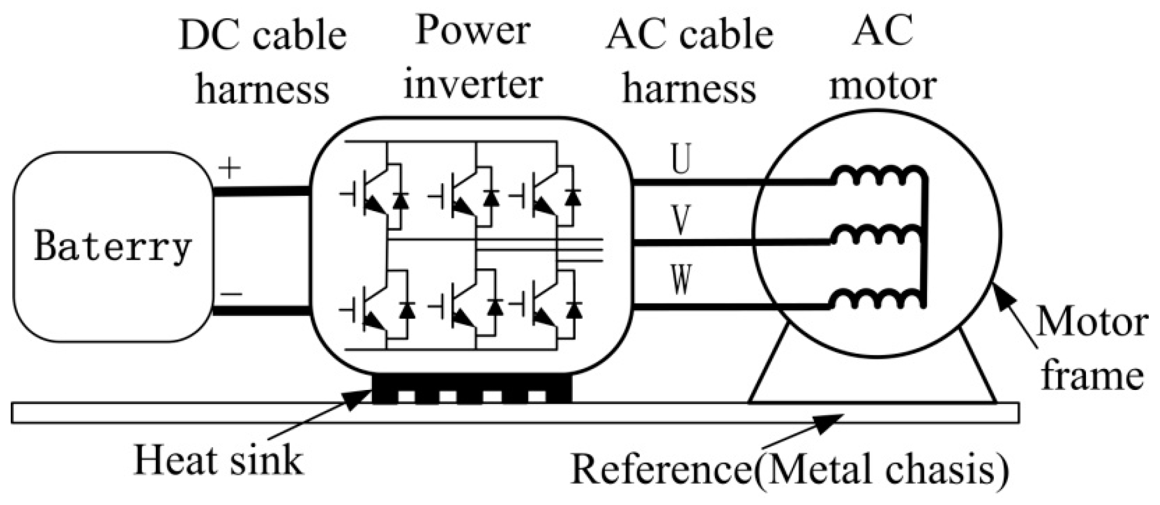
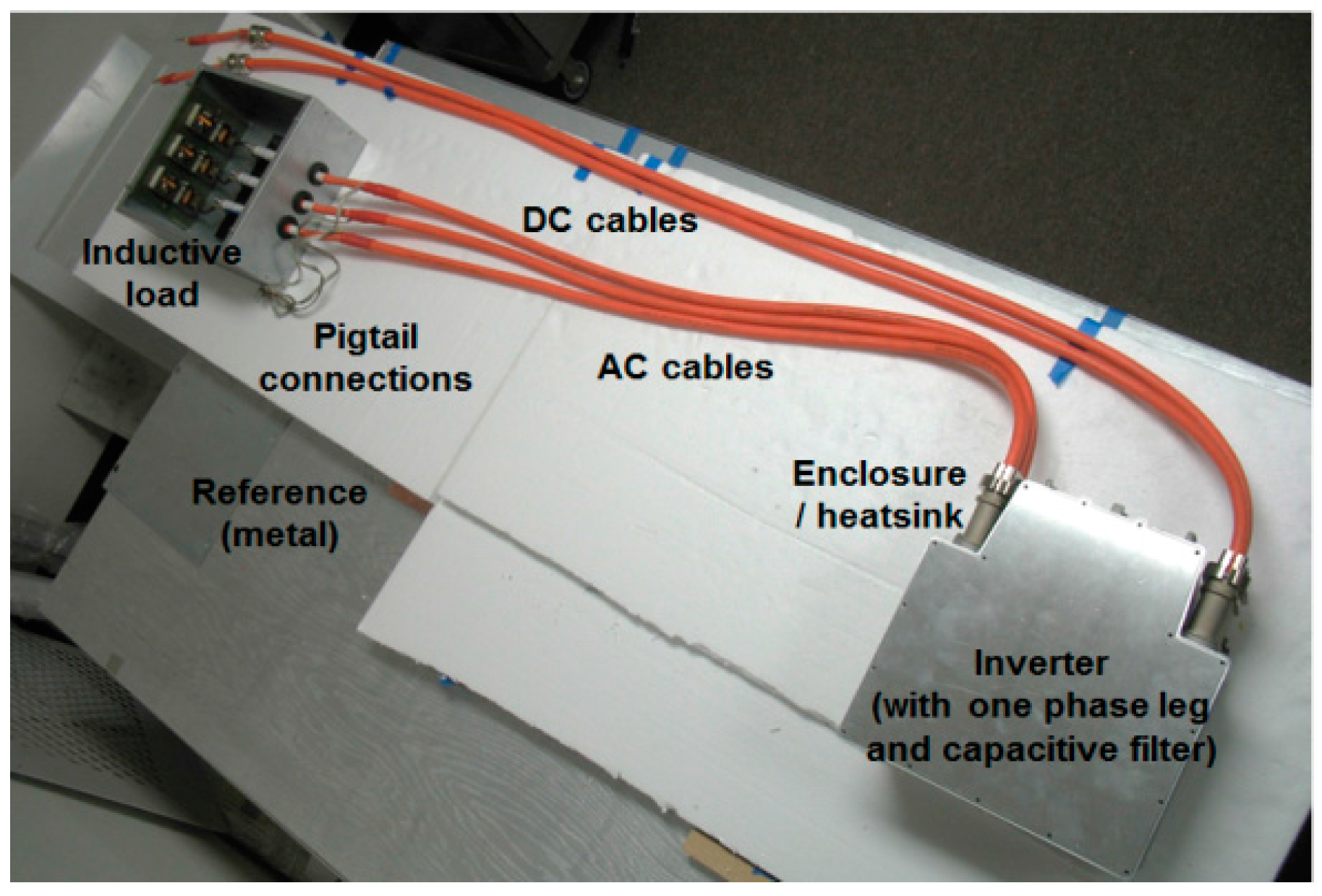
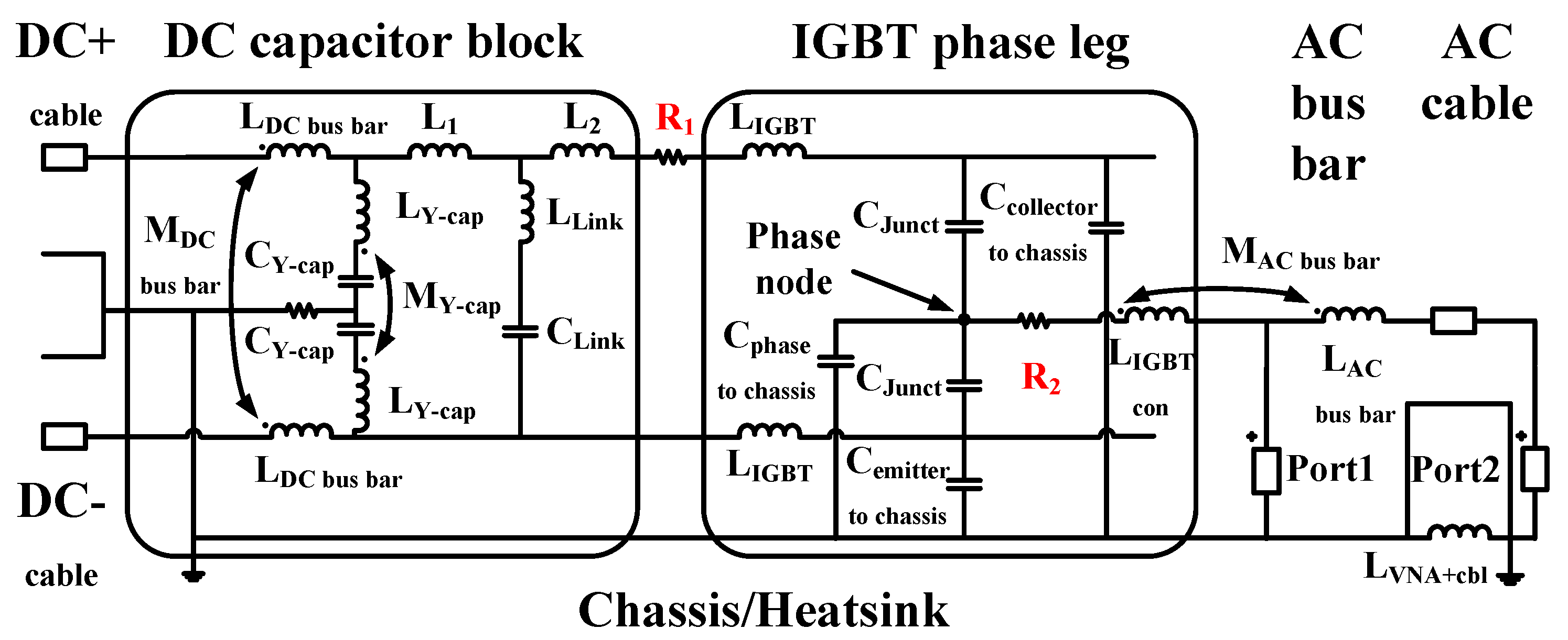
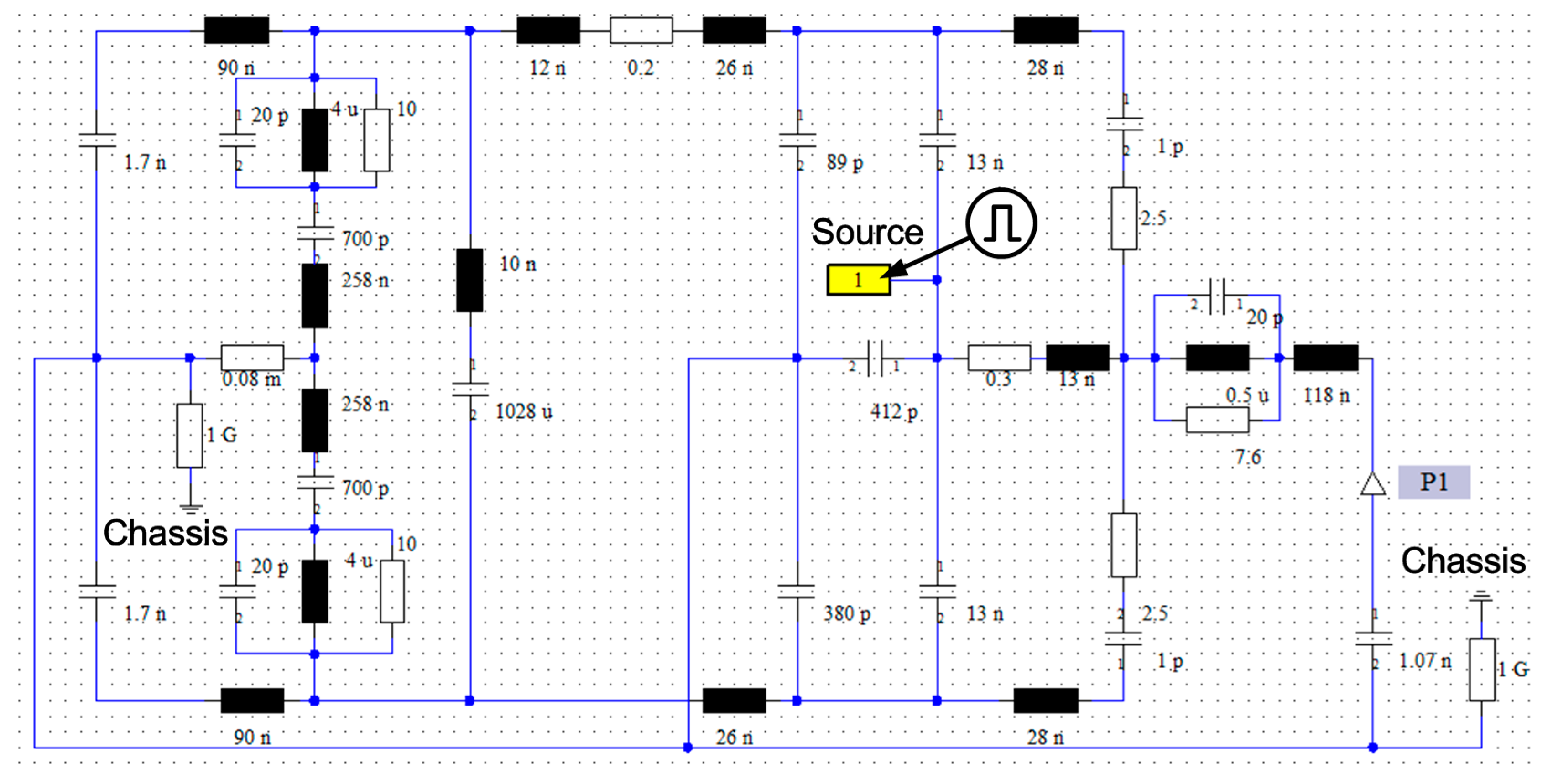
2. Construction of the Power Inverter System

AC motors are widely used in EVs for its advantages of high energy density and high efficiency. The power inverter system for the AC motor is mainly composed of batteries, DC cables, a power inverter, AC cables, and an AC motor, as shown in Figure 1. The fast switching of IGBTs in the power inverter always produce high values of dv/dt and di/dt, which may induce CM interference by parasitic parameters between the power inverter system and chassis in EVs. Due to the CM interference, the conducted electromagnetic emissions of the DC cables of the power inverter system not only may easily exceed the emission limits in a frequency range of 150 kHz to 108 MHz, as defined in the international special committee on radio interference (CISPR25) standard, but also may impact the normal characteristics of batteries and motors, and may even destroy them [24,25]. In addition, the radiation emission generated from the DC cables and the AC cables can interfere with other board equipment and nearby vehicles.
The influence of the CM-conducted emission generated when IGBTs switch on the AC subsystem, including the AC cables and the AC motor, is studied in this paper. The equivalent circuit of the single bridge of the IGBT modules is presented to study the CM-conducted emission transmitting to the AC cables for the topology symmetry of the IGBT modules in the power inverter and the complexity of three bridges working at the same time. A measurement platform was built as shown in Figure 2 to validate the complete equivalent circuit.

3. System Modeling and Analysis

A measurement-based SPICE model of the electromagnetic emissions from the inverter system was built and had a correlation between parasitic circuit elements and system geometry. Parameters of parasitic circuit elements in the model listed in Table 1 [23] were determined by measurements made with a vector network analyzer (VNA) and a time-domain reflector (TDR). The impedance of equivalent series resistance (ESR) of CY-cap and CLink is much smaller than the impedance of equivalent series inductance (ESL) of CY-cap and CLink and thus small enough to be neglected. The impedance of ESR of the capacitors of high-speed switching IGBT is also small enough to be neglected. The inverter system was modeled as a two-port network system, as illustrated in Figure 3. Port 1 was placed between the phase node of two IGBTs of a single bridge leg and the chassis, where the CM voltage at Port 1 is generated by IGBT switching. Port 2 was placed between the center conductor and the shield of a single-phase AC cable, which is connected to the chassis. LVNA + cb1 was the inductance in the measurement cable of the VNA and shorted through the shield of the single phase of the AC cable. The CM voltage at the end of the AC cable was generated to drive the radiated emissions of the parasitic CM antenna. The CM EMI source, and the propagation and mitigation mechanisms, can be achieved through the transfer characteristic between the two ports. The value of S21 between the phase-node-to-chassis voltage and the center-conductor-to-shield voltage of the AC cable connecting to the motor was critical for analyzing the influence of the CM voltage at Port 1 on the CM voltage at Port 2. The system model was validated using the measurement platform shown in Figure 2 [23]. Measured and simulated values of S21 and Z11 are presented in Figure 4, from which the values of S21 and Z11 are closely related. S21 is the forward transfer coefficient of the two-port network circuit, and the ratio of the CM voltage at Port 2 to the CM voltage at Port 1. Therefore, the magnitude of S21 was reduced to lower the CM voltage at Port 2. Since Z11 and S21 are closely related and highly dependent on the impedance looking into the IGBT, Z11 was studied to identify the causes of the resonances. From Figure 4, these approximations were used to help guide the analysis [23].
The magnitudes of S21 and Z11 suggest that parallel resonances in the equivalent circuit of the power inverter can occur at 6, 11, and 26 MHz. It is critical to understand the high frequency components or current paths involved in the three parallel resonances. Port 1 was supposed to be a CM noise current source. The CM noise current paths at 6, 11, and 26 MHz were studied, and the equivalent circuits were built, respectively. It is critical to identify the elements responsible for parallel resonances based on the impedance information at the resonance frequency points, of which the Z11 has the maximum magnitude. The capacitances and inductances generating the parallel resonances at those frequencies and responsible elements were determined to mitigate the CM conducted emission by IGBT switching and reduce the radiated emission of the AC cables.

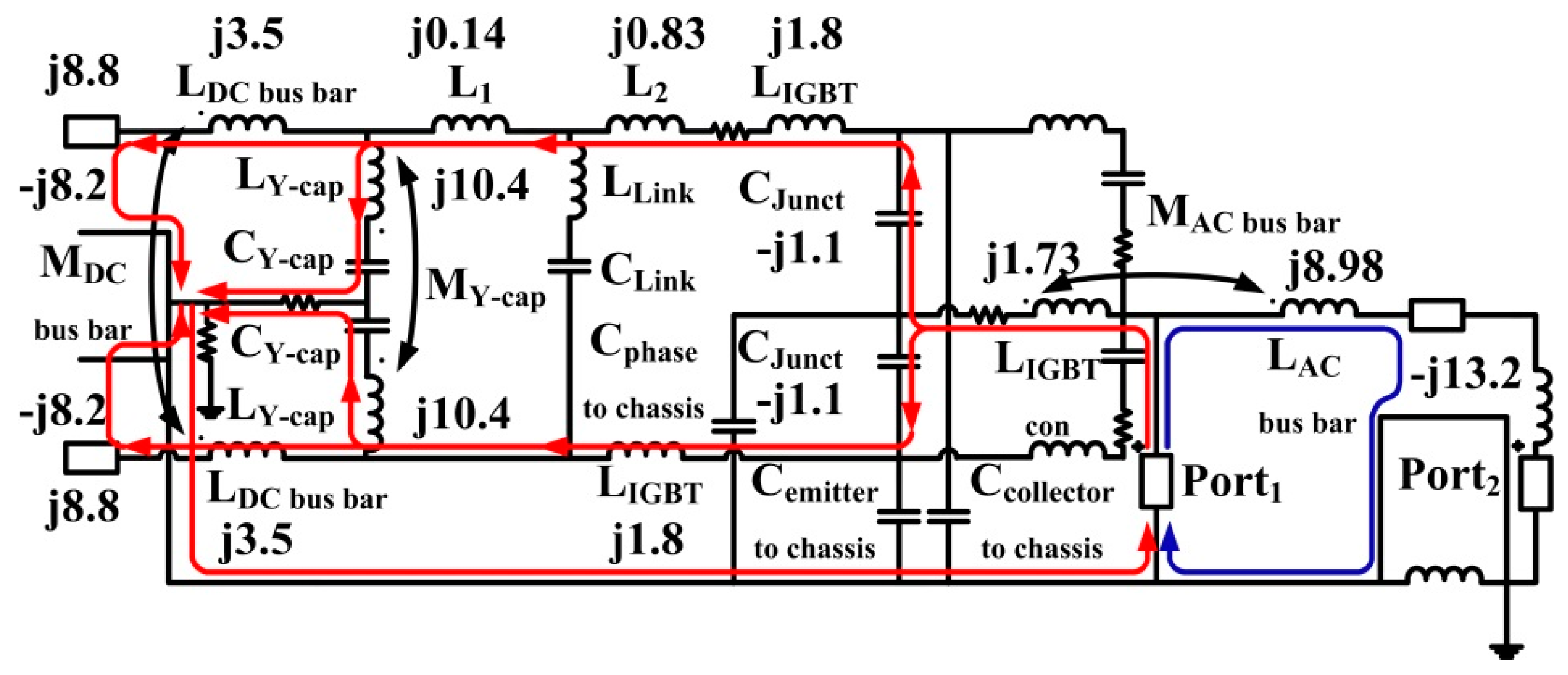
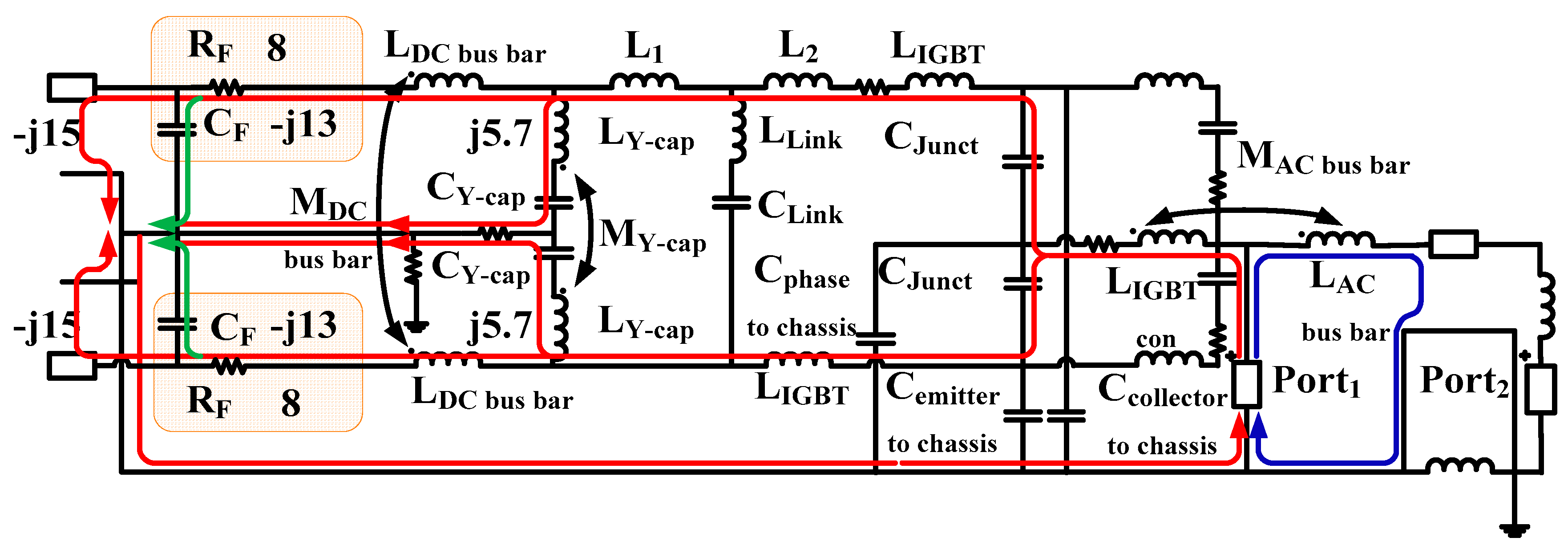
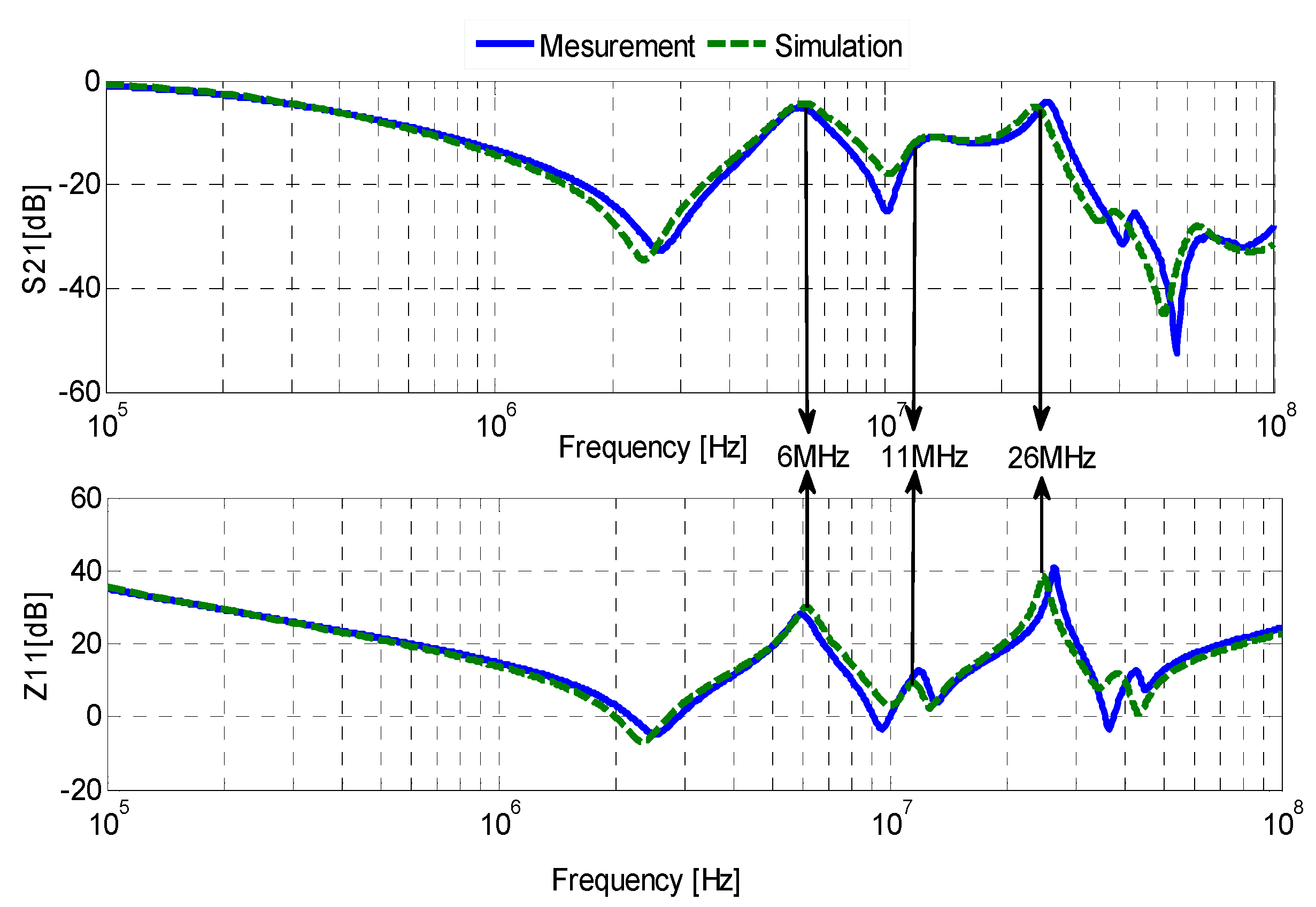
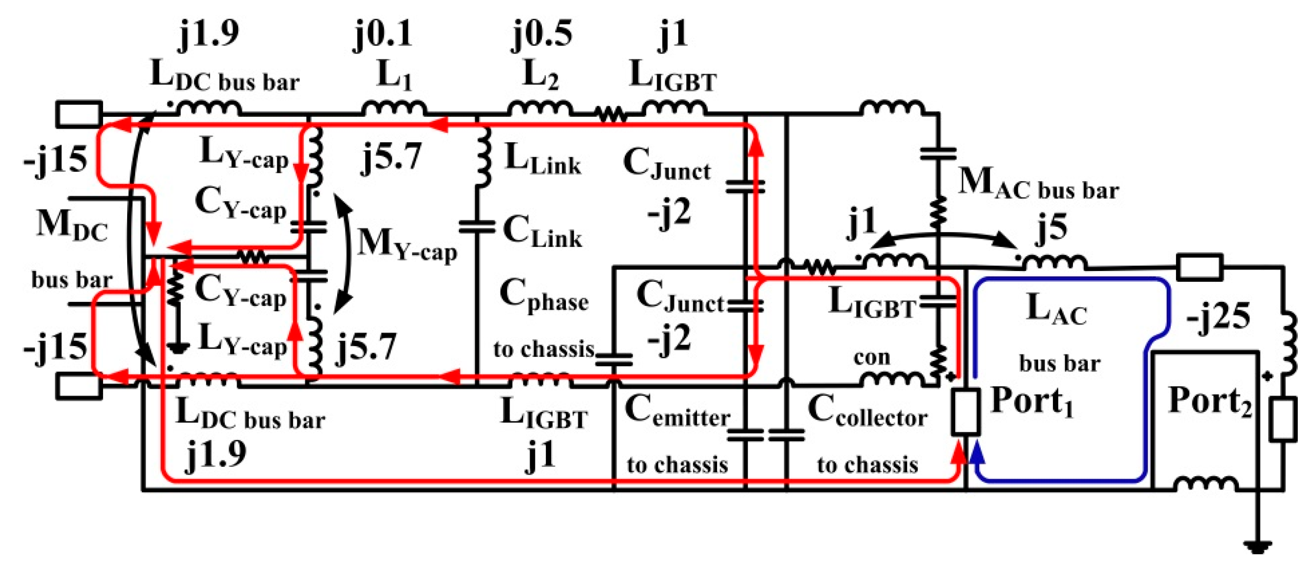
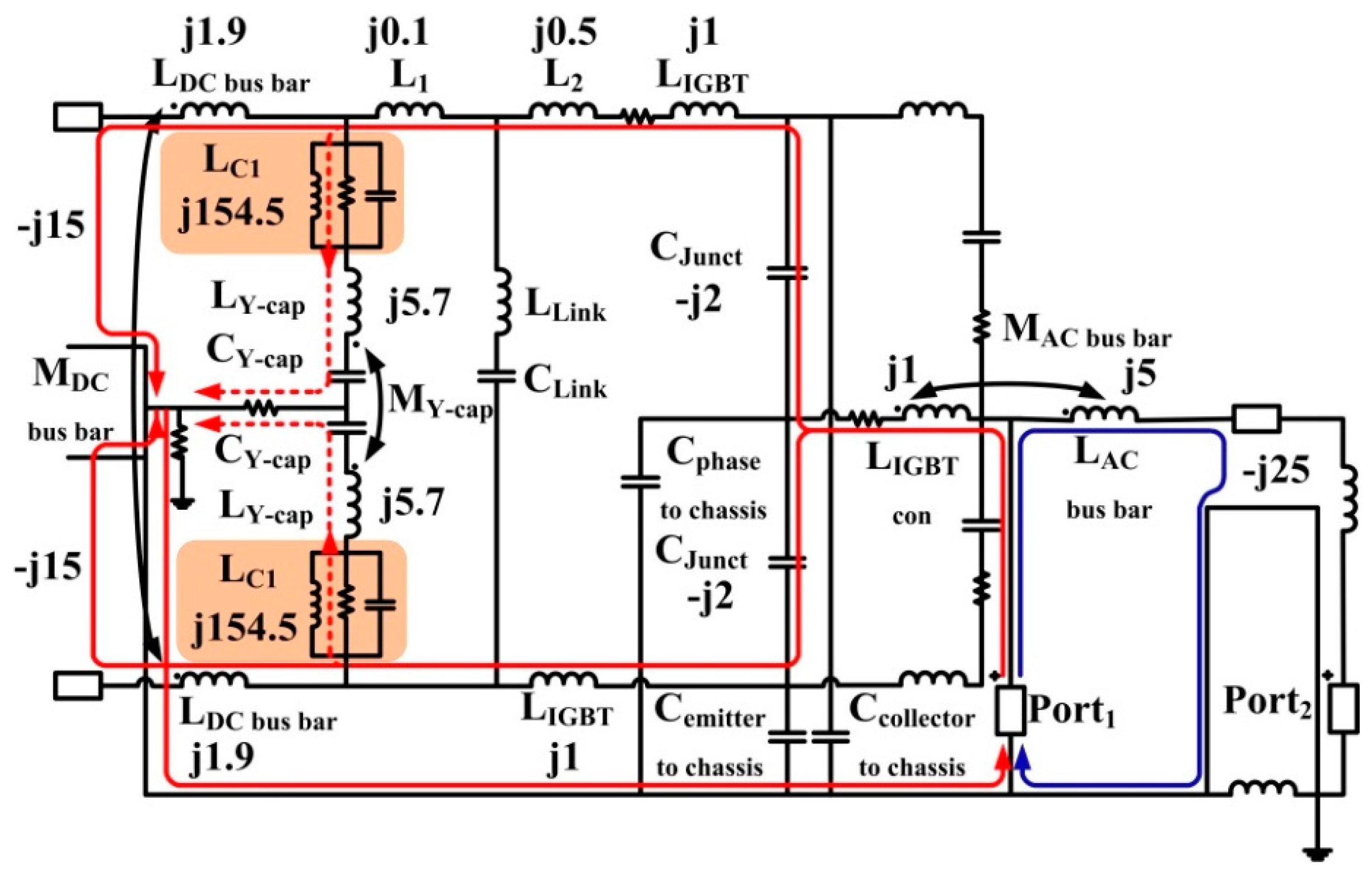
3.1. Analysis of Current Path for 6 MHz

The impedance of each circuit element at 6 MHz was calculated as shown in Figure 5 to find the elements responsible for the resonance at 6 MHz. Port 1 between the phase node and chassis was supposed to be a CM current source, and the CM current paths for 6 MHz are shown in Figure 5. The current paths were mainly composed of a DC side path and an AC side path. However, only the DC side current flowing path was analyzed due to the fact that the impedance of the AC side circuit was about –j25 Ω and much higher than that of the DC side, as shown in Figure 6. The CM current flowed from the plus of Port 1 to the plus and minus of the DC cables symmetrically through junction capacitance across both the pull-up and pull-down IGBT Cjunct and resulted in two current flowing paths. Each path was divided into two parallel paths through LIGBT. One path was through the DC bus bar and the DC cable to the chassis, and the other path was through Y-cap to the chassis. Finally, the CM current flowed back to the minus of Port 1. The impedance of the DC cable was about −j15 Ω and mainly capacitive at 6 MHz for its impedance characteristic [23]. The impedance of the DC bus bars was about j 2 π f ( L DC bus bar + M DC bus bar ) = 2 π 6 e 6 Hz ( 50 n H + 40 n H ) j 3.4 Ω , so the effective impedance for the path was −j11.6 Ω and −j5.8 Ω with the two paths in parallel. The capacitance of the Y-cap was very small and can be negligible, and the inductance of the Y-cap was about j 2 π f ( L + M ) = 2 π 6 e 6 Hz ( 150 n H + 108 n H ) j 10   Ω , so the impedance of the two branches in parallel of Y-caps was inductive as j5 Ω. Finally, the capacitive reactance of the DC bus bars path (−j5.8 Ω) resonated with the inductive reactance of Y-cap path (j5 Ω).
It is obvious that the capacitances of the two parallel branches due to the DC cable and the DC bus bar could generate a parallel resonance with the inductances of the two parallel branches due to the Y-cap. Therefore, the elements responsible for the resonance at 6 MHz were mainly the capacitances of the DC cables, the inductances of the DC bus bar, and the inductances of the Y-cap.

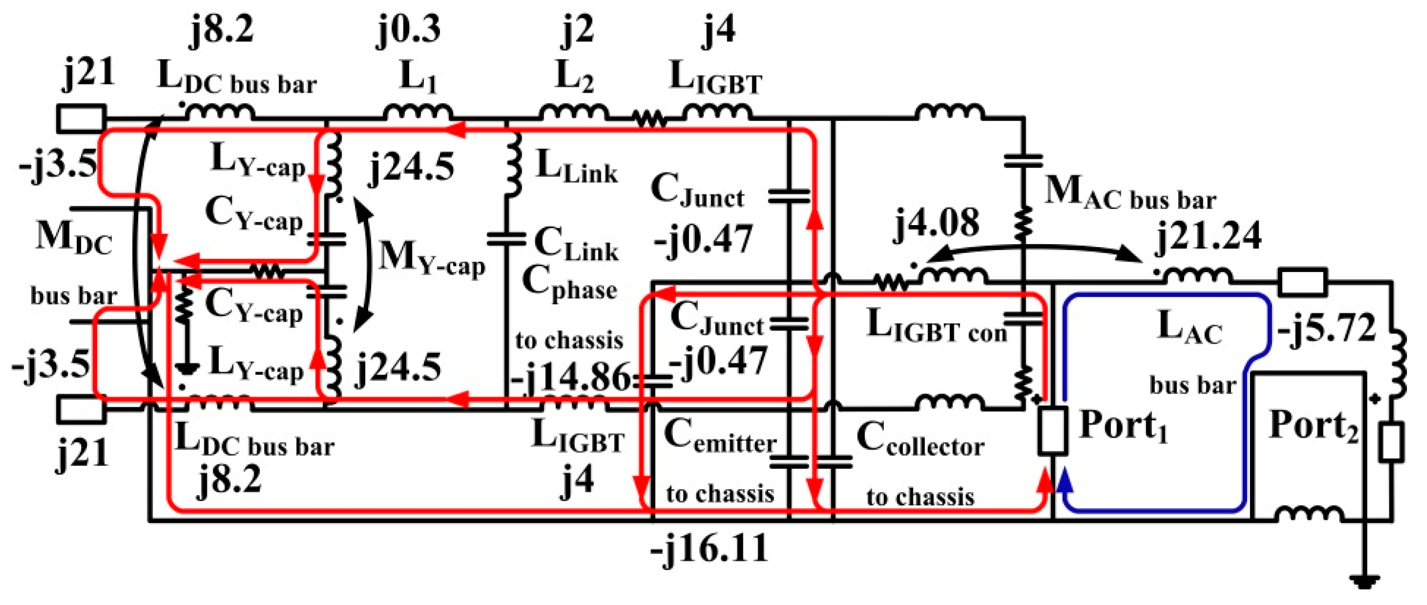
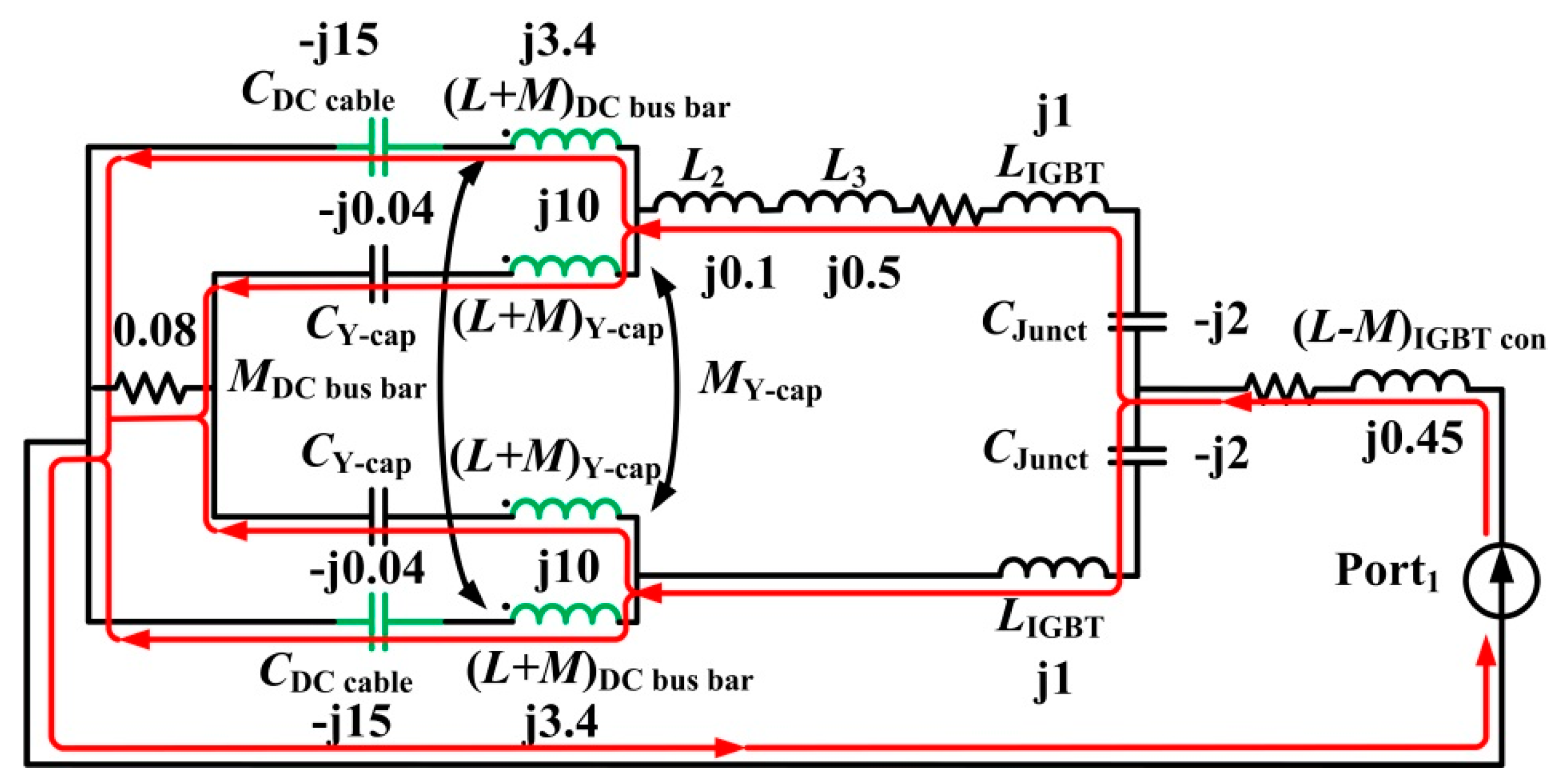
3.2. Analysis of Current Path for 11 MHz

The current flowing paths at 11 MHz were mainly composed of a DC side path and an AC side path, which is similar to that at 6 MHz, as shown in Figure 7. However, the impedance of capacitance and inductance of the DC cables at 11 MHz were about −j8.2 Ω and j8.8 Ω, respectively. One DC side current path was through the DC bus bar and the DC cable to the chassis, and the other path is through the Y-cap to the chassis. The CM current of the AC side flowed from the plus of Port 1 to the AC bus bar and the AC cable and back to the minus of Port 1. The impedances of the AC side circuit and the DC side circuit were about −j5 Ω and j4.5 Ω, shown in Figure 8, which are close. Therefore, the AC side current path could not be neglected. The effective inductance of the DC side circuit generated a parallel resonance with the effective capacitance of the AC side. Therefore, the elements responsible for the resonance at 11 MHz were mainly the capacitances of the DC cables, the inductances of the DC bus bar, the inductances of the Y-cap, the inductances of the AC bus bar, and the capacitances of the AC cable.

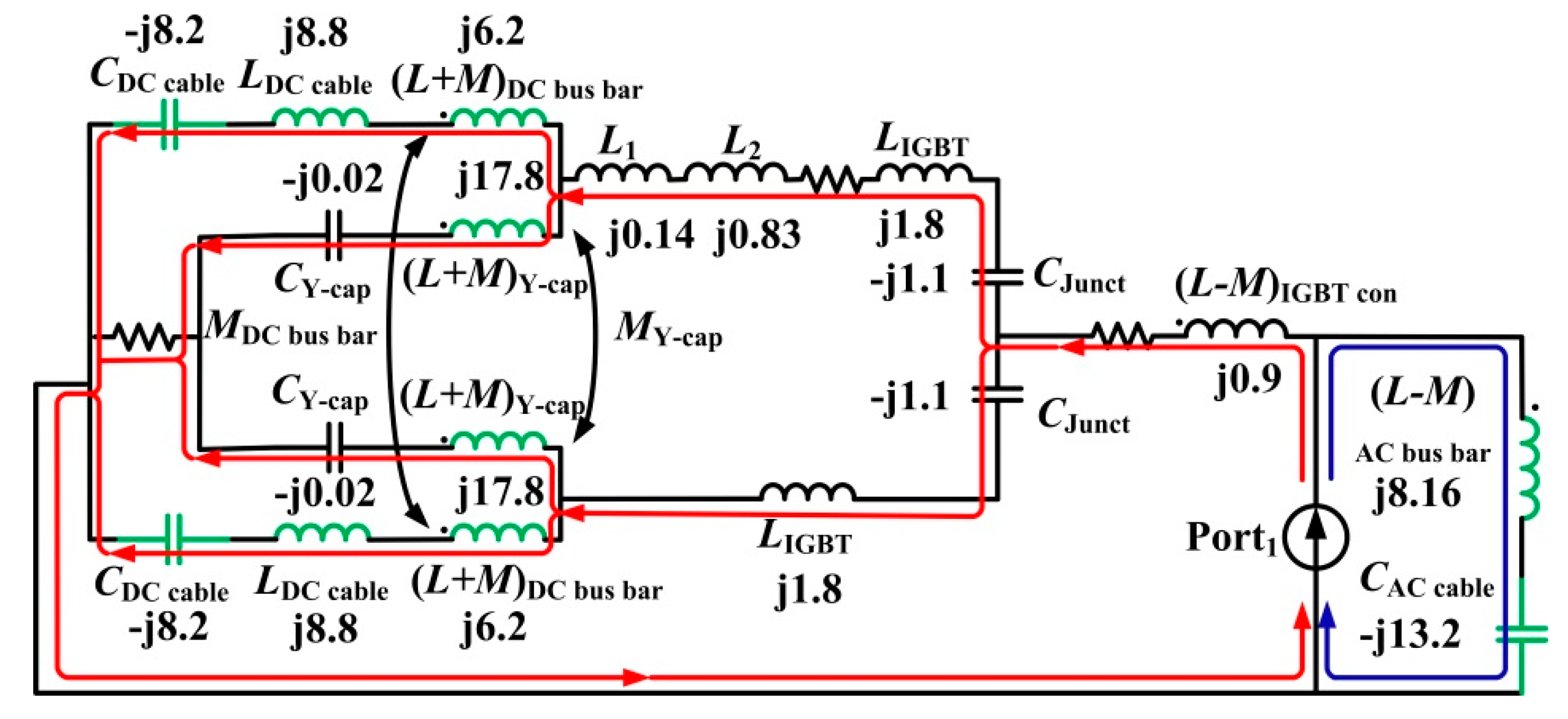
3.3. Analysis of Current Path for 26 MHz

The CM current flowing paths at 26 MHz were also composed of a DC side path and an AC side path shown in Figure 9. However, the DC side path at 26 MHz was different from that at 6 MHz and 11 MHz due to the CM current flowing to the chassis not only from the DC bus bar, the DC cables, and the Y-cap, but also the distributed capacitance from the phase node to the chassis (Cphase to chassis, Ccollector to chassis, and Cemitter to chassis). Equivalent circuit for 26 MHz is shown in Figure 10, where current Loop1, current Loop2, and current Loop3 are considered in parallel. The effective impedance of inductance for the three current loops in parallel was about j6 Ω, and the effective impedance of capacitance for the fourth current loop dominated by Cphase to chassis, Ccollector to chassis, and Cemitter to chassis was about −j5.7 Ω. Therefore, the elements responsible for the resonance at 26 MHz were mainly the capacitance of the DC cables, the inductance of the DC bus bar, the inductances of the Y-cap, the capacitance of the IGBT phase node to the chassis, the capacitance from IGBT emitter to the chassis, the capacitance of the AC cable, and the inductance of the AC bus bar. The elements responsible for critical resonances at about 6, 11, and 26 MHz are listed in Table 2.

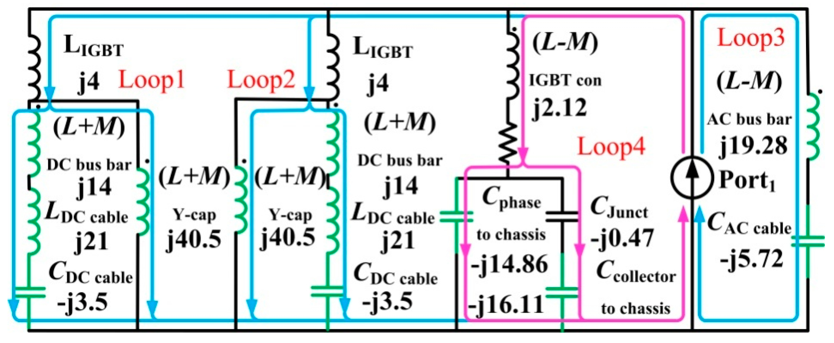
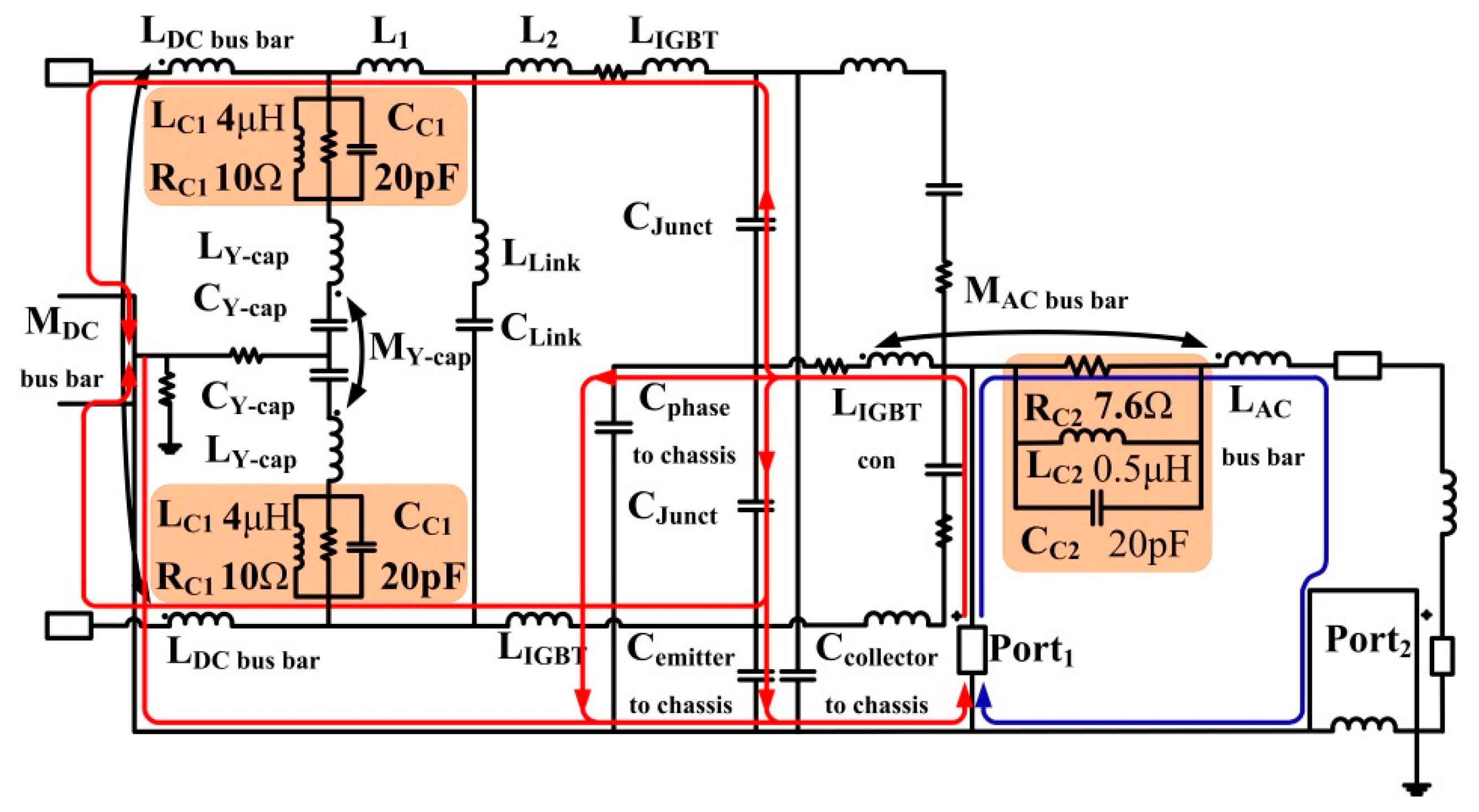
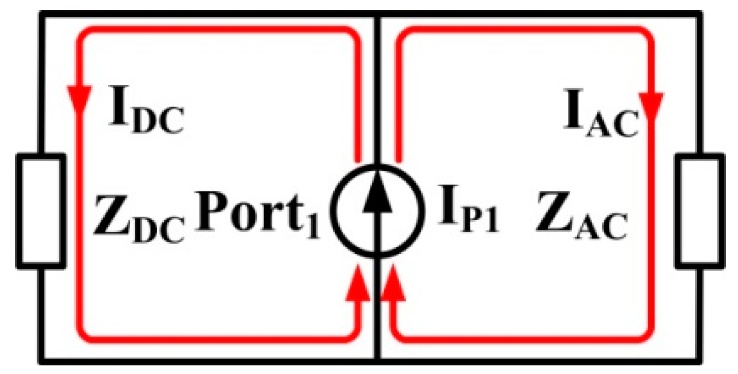
4. Mitigation of System Resonances

According to the analysis of current paths at 6 MHz, 11 MHz, and 26 MHz, the CM emission from the phase node of the two IGBTs of one phase bridge leg of the IGBT module due to fast IGBT switching can be equivalent to a current source, as shown in Figure 11. CM noise current IP1 is mainly composed of two current flowing paths—one is through the DC side elements, another one is through the AC side elements. As shown in Figure 11, it is expressed as
I P 1 = I DC + I AC ,   and
I DC Z DC = I AC Z AC
where IDC is the current of the DC side, ZDC is the equivalent impedance of the DC side, IAC is the current of the AC side, and ZAC is the equivalent impedance of the AC side. Z11 is the effective impedance of Port 1, as well as the parallel impedance of ZDC and ZAC, as shown in Equation (3). The relationship between IP1 and the CM noise current of the AC side IAC is expressed as Equation (4). Mitigation elements are added in the DC side circuit, and the impedance of the AC side elements composed of the AC bus bar and the AC cables is supposed to be constant. Therefore, it is shown that the CM current flowing on the AC cable is proportional to the magnitude of Z11 according to Equation (5).
Z 11 = Z DC Z AC Z DC + Z AC
I AC I P 1 = Z DC Z DC + Z AC = Z 11 Z AC ,   and
I AC I AC - = Z 11 Z 11 -
where Z11 and Z11- are the effective impedance magnitude of Port 1 without and with mitigation elements, IAC and IAC- are the effective CM current of the AC side circuit without and with mitigation elements.

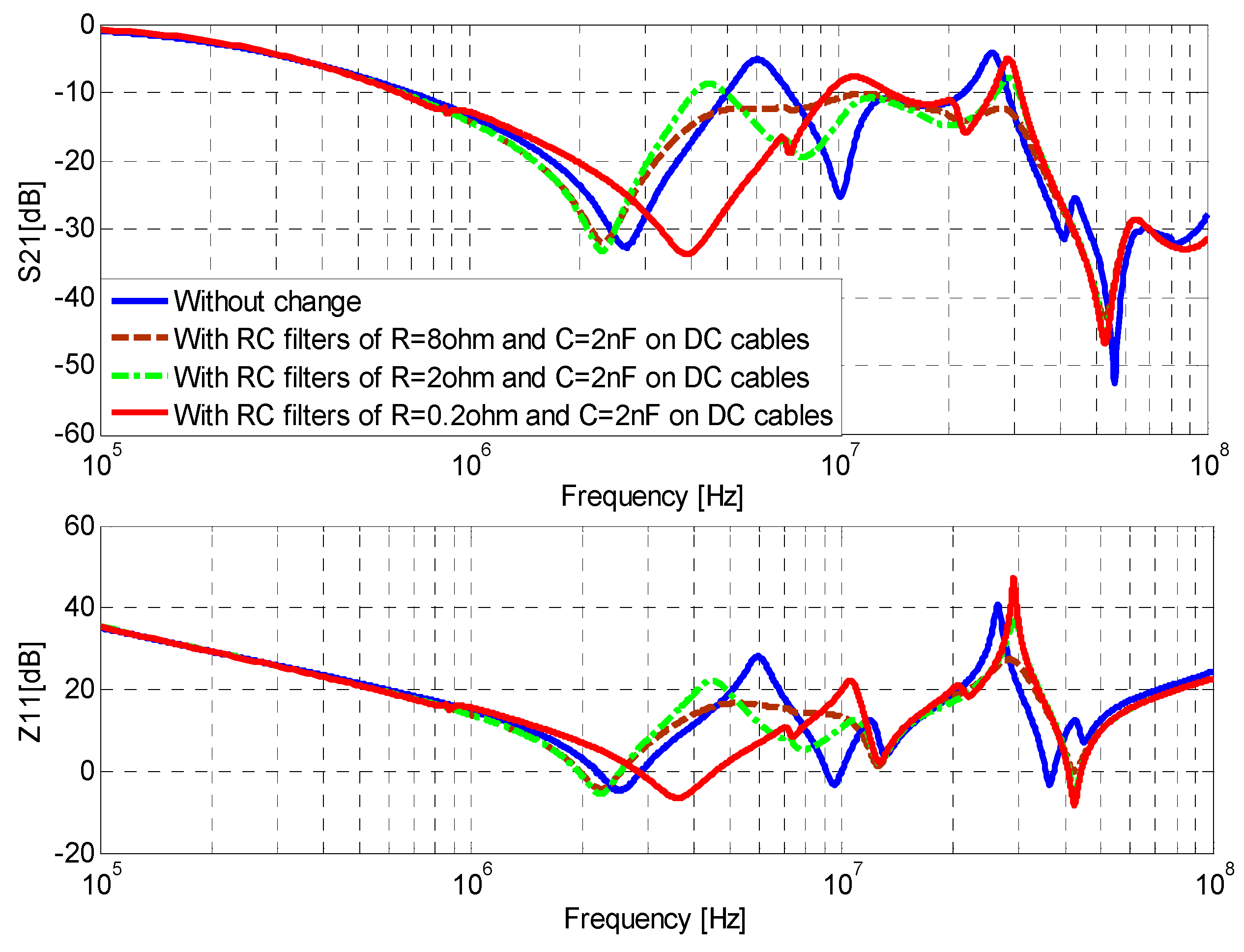
4.1. Mitigation Circuit Design at 6 MHz

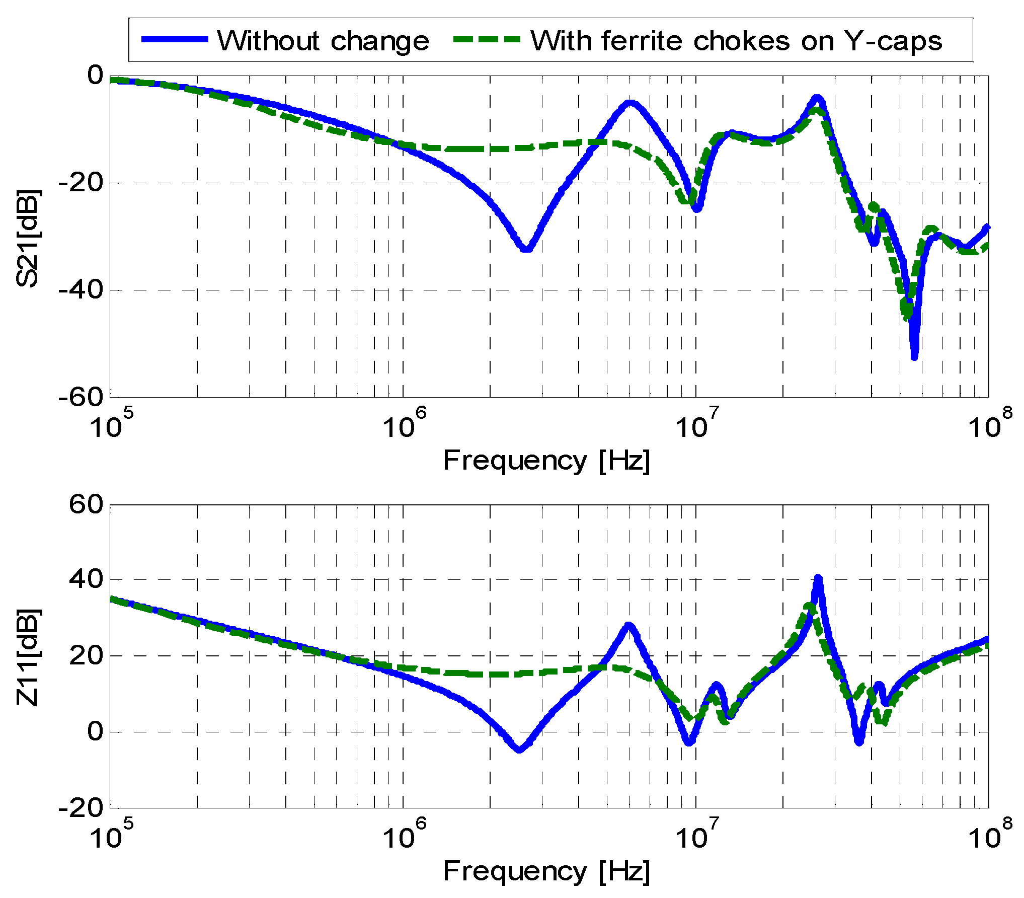
4.1.1. Design of CM Ferrite Choke

From Figure 4, since the magnitude of Z11 is low at 11 MHz, mitigation circuits were designed at resonance frequencies 6 MHz and 26 MHz. According to Table 2 and Figure 6, the capacitances between the DC cables and the shield CDC cable, or the inductance of the DC bus bar LDC bus bar and the inductance of the Y-cap LY-cap, can be changed to decrease the magnitude of Z11 and to reduce the value of the resonance at 6 MHz.
A CM ferrite choke through the Y-cap was added to change the effective inductance of the branch to reduce the magnitude of Z11 at 6 MHz, and to reduce the CM current and the radiated emission through the AC cable. If the value of Z11 is expected to reduce by K times, then
Z 11 6 Z 11 - 1 6 = K Z 11 6 ( dB ) Z 11 - 1 6 ( dB ) = 20   log   K
where Z 11 6 and Z 11 - 1 6 are the magnitude of Z11 at 6 MHz without and with a CM ferrite choke. From Figure 4, Z 11 6 ( dB ) = 30   dB ; if K = 5, then Z 11 - 1 6 ( dB ) = 16   dB . The ferrite choke is modeled as a simple parallel RLC circuit, L C 1 is the inductance of the CM ferrite choke, and Z 11 6 and Z 11 - 1 6 will be expressed as
Z 11 6 = Z DC Z Y + Z IGBT ( Z DC + Z Y ) 2 ( Z DC + Z Y ) + R + Z IGBTcon ,   and
Z 11 - 1 6 = Z DC ( Z Y + Z L C 1 ) + Z IGBT ( Z DC + Z Y + Z L C 1 ) 2 ( Z DC + Z Y + Z L C 1 ) + R + Z IGBTcon ,
where Z DC is the impedance of CDC cable and (L + M)DC bus bar, Z Y is the impedance of CY-cap and (L + M)Y-cap in series, Z IGBT is the impedance of LIGBT and CJunct in series, L2 and L3 are negligible, R = 0.3   Ω , Z IGBTcon is the impedance of LIGBT con, and Z L C 1 is the impedance of L C 1 . From Equation (8) and the impedance of circuit elements in Figure 6, we can achieve
Z 11 - 1 6 = | Z DC ( Z Y + Z L C 1 ) + ( Z IGBT + Z Junct ) ( Z DC + Z Y + Z L C 1 ) 2 ( Z DC + Z Y + Z L C 1 ) + R + Z IGBTcon | = | j 11.6 ( j 10 + Z L C 1 ) j ( j 11.6 + j 10 + Z L C 1 ) 2 ( j 11.6 + j 10 + Z L C 1 ) + 0.3 + j 0.45 | = 6.3 Z L C 1 = 154.5 Ω , L C 1 = Z L C 2 π 6 e 6 = 4 μ H
From Equation (9), a CM ferrite choke ( L C 1 = 4   μ H , R C 1 = 10   Ω , C C 1 = 20   pF ) simplified as a parallel RLC circuit was chosen, as shown in Figure 12 [26]. After adding the equivalent circuit model of the CM ferrite choke in the ADS PSPICE model, the CM current could no longer flow through the Y-cap to the chassis due to the large impedance of L C 1 at 6 MHz, as shown in Figure 12. From the simulation results shown in Figure 13, the values of Z11 and IAC are reduced by 14 dB and meet the design requirement, and the value of S21 between Port 1 and Port 2 is reduced by 7.2 dB, which shows that the CM current and the radiated emission through the AC cable generated by fast IGBT switching can be reduced by adding an appropriate CM ferrite choke through the Y-caps.

4.1.2. Design of RC Filter

An RC filter in front of DC cables was added to change CDC cable and to reduce the magnitude of Z11 at 6 MHz and the quality factor of the resonance Q. It can be expressed as
Z 11 6 Z 11 - 2 6 = K Z 11 6 ( dB ) Z 11 - 2 6 ( dB ) = 20   log   K
where Z 11 6 and Z 11 - 2 6 are the magnitude of Z11 at 6 MHz without and with an RC filter. If K = 5, Z 11 6 and Z 11 - 2 6 can be expressed as
Z 11 6 = Z DC Z Y + Z IGBT ( Z DC + Z Y ) 2 ( Z DC + Z Y ) + R + Z IGBTcon ,   and
Z 11 - 2 6 = Z DC Z Y + Z IGBT ( Z DC + Z Y ) 2 ( Z DC + Z Y ) + R + Z IGBTcon
where Z D C = ( Z DC cable × Z C F ) / ( Z DC cable + Z C F ) + Z DC bus bar , C F is the capacitance of the RC filter, and Z C F is the impedance of C F . From Equation (12) and the impedance of circuit elements in Figure 6, we can achieve
Z 11 - 2 6 = | Z DC Z Y + Z IGBT ( Z DC + Z Y ) 2 ( Z DC + Z Y ) + R + Z IGBTcon | = 6.3 Z C F = 13.3 Ω C F = 1 2 π 6 e 6 Z C F = 2 nF
The values of RC are chosen as C F = 2   nF , an RC filter with R F = 8   Ω shown in Figure 14. The CM current can flow to the chassis through the RC filter. From the simulation results shown in Figure 15, the values of Z11 and IAC are reduced by 14 dB and the value of S21 is reduced by 8 dB, which indicates that adding an appropriate RC filter in front of the DC cables can reduce the emission and resonance peak at 6 MHz. However, the working current on the DC cables is generally higher than 100A, and the voltage and consuming energy of R F is high using the resistance ( R F = 8   Ω ). Therefore, R F should be low enough to guarantee that the system works normally. From simulation results shown in Figure 15, although the magnitude of Z11 decreases at 6 MHz, the magnitude of Z11 at 11 MHz and 26 MHz both increase using the RC filer ( C F = 2   nF and R F = 0.2   Ω ). As a result, it is not recommended that an RC filter is added in front of the DC cables to reduce the CM current or the radiated emission through the AC cable.

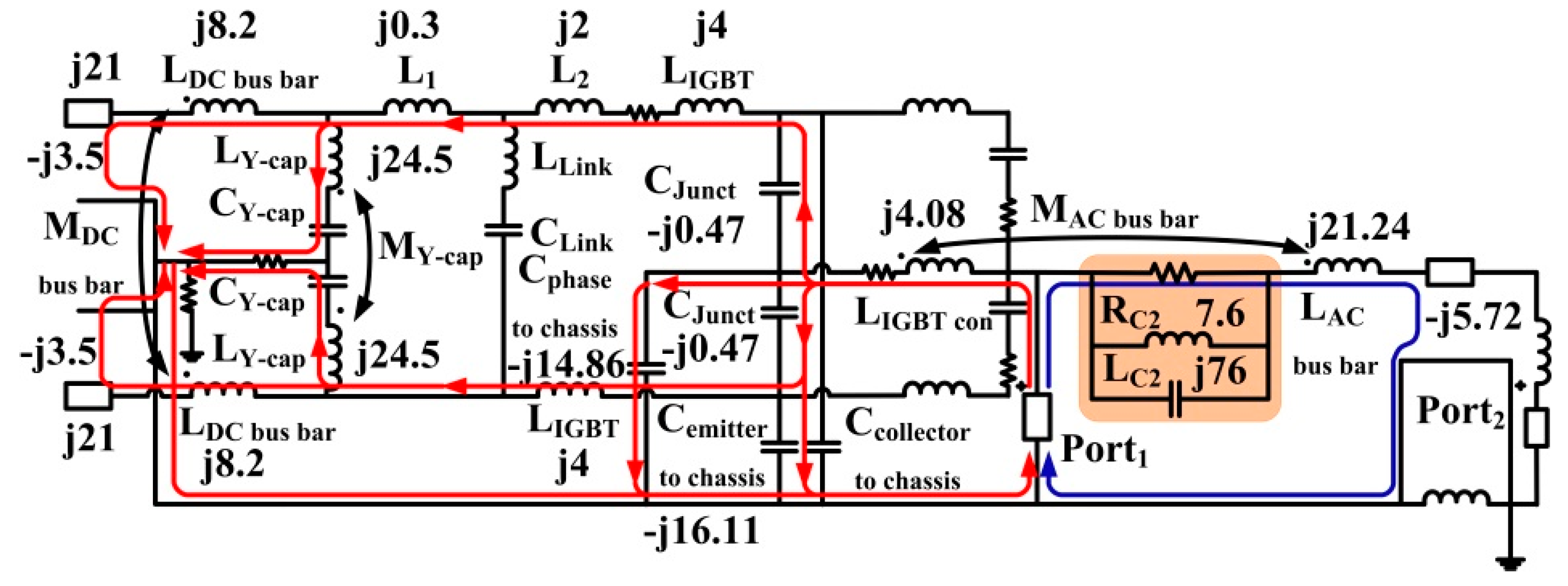
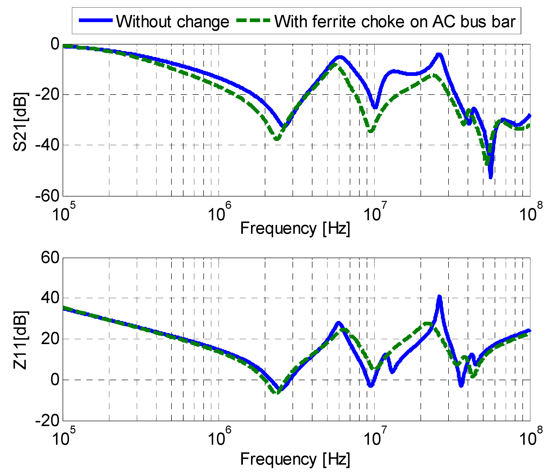
4.2. Mitigation Circuit Design at 26 MHz

A CM ferrite choke was added to the AC bus bar due to the impedance of LAC bus bar larger than other elements in the equivalent circuit at 26 MHz resonance. Therefore, the CM ferrite choke is designed by calculating ZDC and ZAC, as shown in Equation (14).
I AC I P1 = Z DC Z DC + Z AC
The impact of resonances within the power inverter can be reduced by transferring the resonance frequencies to an unimportant range through changing the capacitances and inductances generating resonances, or in some cases by reducing their quality factor, for example, reducing the resistance of Z11 at the 26 MHz resonance. The inductance of the CM choke is very high at 26 MHz due to the high-frequency CM current, and the resistance of the CM is more critical than the inductance at the time, so the CM choke is designed by the expected resistance R C 2 . If a CM choke is added in the AC side circuit, and IAC is expected to reduce by K times, then:
I AC 26 I AC - 1 26 = K I AC 26 ( dB ) I AC - 1 26 ( dB ) = 20   log   K
where I AC 26 and I AC - 1 26 are the amplitude of IAC at 26 MHz without and with a CM ferrite choke. As shown in Figure 11, the relationship of the noise current and the impedance before and after the mitigation is:
I AC 26 I AC - 1 26 = Z DC - 1 26 + Z AC - 1 26 Z DC 26 + Z AC 26
where Z DC 26 and Z DC - 1 26 - are the magnitude of ZDC at 26 MHz without and with a CM ferrite choke, respectively. Z AC 26 and Z AC - 1 26 are the magnitude of ZAC at 26 MHz without and with a CM ferrite choke, respectively. From Equation (14) and the impedance of circuit elements in Figure 10, we can achieve
I AC 26 I AC - 1 26 = Z DC - 1 26 + Z AC - 1 26 Z DC 26 + Z AC 26 = Z DC 26 + Z AC 26 + R C 2 Z DC 26 + Z AC 26 | - j 12 + j 13.56 + R C 2 - j 12 + j 13.56 | = K = 5 R C 2 = 7.6 Ω
where Z DC 26 = j 12 Ω and Z AC 26 = j 12.56 Ω .
In order to prevent the CM current from flowing through the inductance of the choke, the impedance of the inductance should be ten times more than that of the resistance of the choke; thus, Z L C 2 = 2 π 26 e 6 L C 2 10 R C 2 = 76   Ω and L C 2 0.47   μ H . Furthermore, the inductance of the choke should be far lower than that of winding of the motor. Finally, the inductance of the choke was determined as 0.5   μ H . A CM ferrite choke ( L C 2 = 0.5   μ H , R C 2 = 7.6   Ω , C C 2 = 20   pF ) simplified as a parallel RLC circuit was chosen, as shown in Figure 16. From the simulation results of Z11 and S21 shown in Figure 17, the magnitude of S21 was reduced by 5 dB, which shows that adding an appropriate CM ferrite choke through the AC bus bar is a better technology for reducing the CM current and the radiated emission through the AC cable.

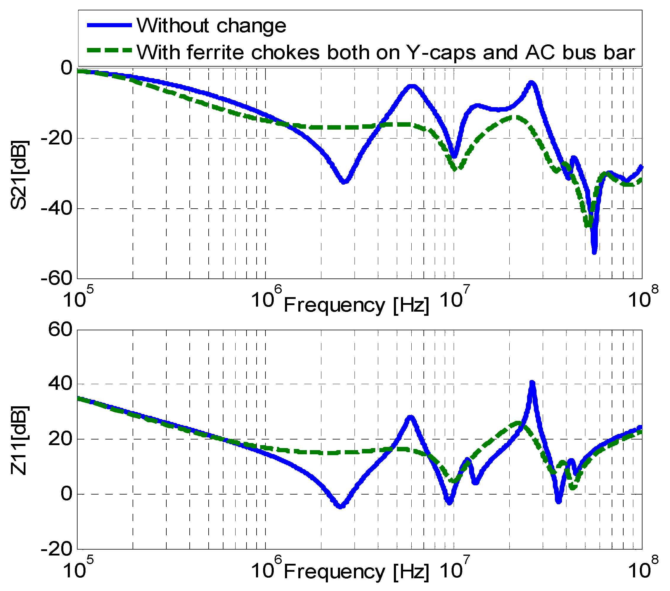
4.3. Combined Mitigation Circuit Design

The impact of a combination mitigation strategy deployed by adding CM ferrite chokes on the Y-caps and the AC bus bar is shown in Figure 18. The values of Z11 and S21 at three critical resonance frequencies about 6, 11, and 26 MHz were significantly reduced, as shown in Figure 19. The values of Z11 are decreased respectively by 15 dB at 6 MHz, 0.4 dB at 11 MHz, and 11.5 dB at 26 MHz, and the values of S11 is decreased respectively by 8.6 dB at 6 MHz, 7 dB at 11 MHz, and 6.3 dB at 26 MHz. It is shown that the combination mitigation is a reasonable technology for reducing the CM current and the radiated emission through the AC cables at the three critical resonance frequencies.

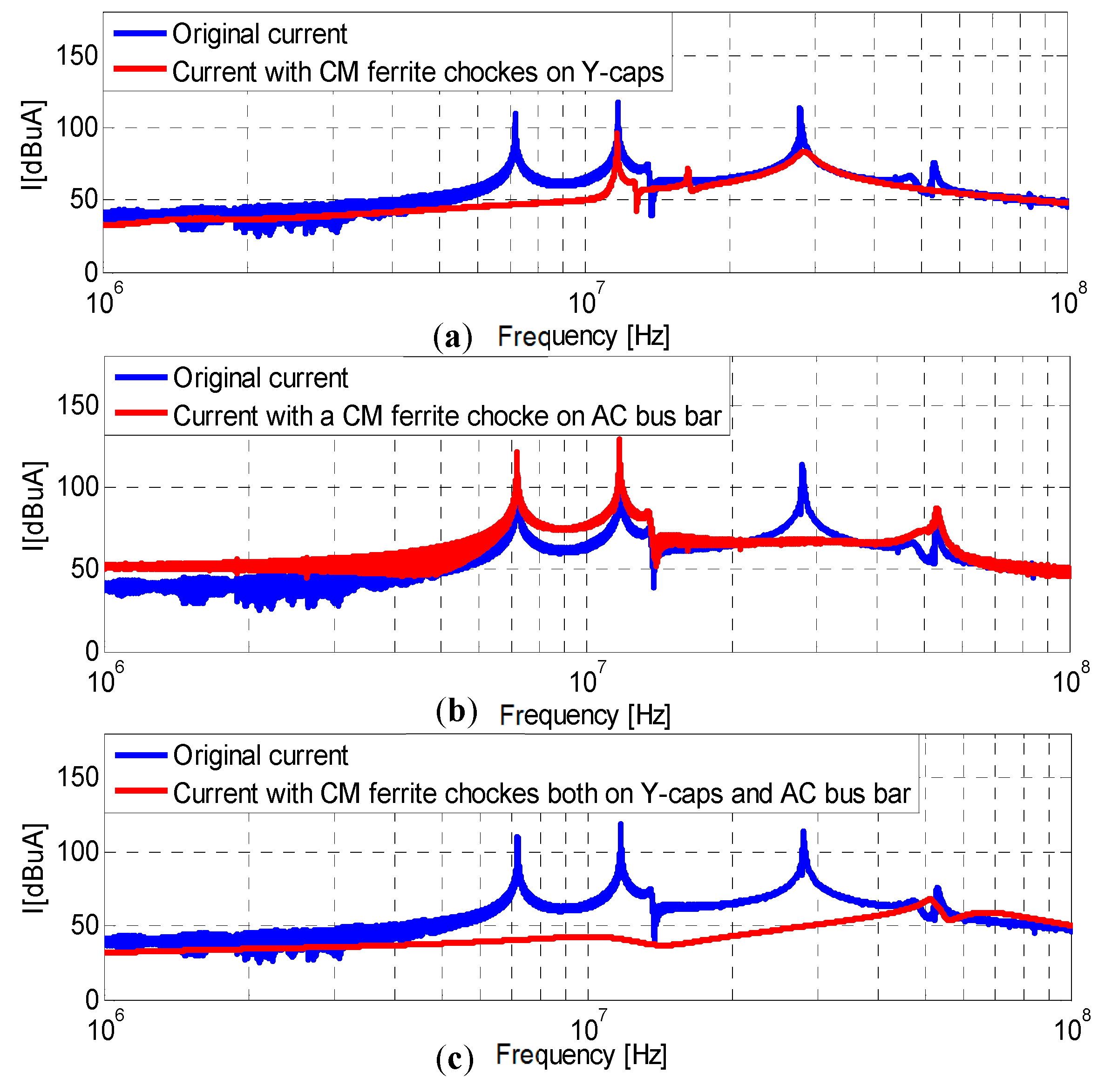
5. Verification of Mitigation Method with Time Domain Simulation

To validate the mitigation technology, a PSPICE model of the power inverter system for a real-time simulation at time domain was built in the CST designer, as shown in Figure 20. A trapezoidal CM interference source was added between the two IGBTs of a single bridge leg as “Source 1.” The cycle time of the trapezoidal wave was 20 μs, and the rise time was 0.032 μs. The probe P1 can obtain the CM current flowing through the AC cable, as shown in Figure 21. The original CM current without any mitigation method is shown as the blue line. There are three problematic resonance frequencies at 7 MHz, 11 MHz, and 26 MHz, similar to that of the model in the ADS software shown in Figure 3.
The value of the CM current flowing through the AC cable at 7 MHz decreased with the CM ferrite choke through the Y-caps, as shown in Figure 21a, the CM current at 26 MHz decreased with a CM ferrite choke through the AC bus bar, as shown in Figure 21b, and the CM current at three problematic resonances all decreased with the CM ferrite chokes through the Y-caps and the AC bus bar, as shown in Figure 21c. The mitigation method was effectively validated by the real-time simulation results at time domain and divided into the following steps: At first, the power inverter system based on measurement was modeled. Secondly, the responsible components for the problematic resonances were determined through the transmission characteristics. Finally, the appropriate mitigation method to reduce emission was designed.

6. Conclusions

The power inverter system for EVs was modeled based on measurements as a two-port network system to analyze the occurring resonances, current paths, and mitigation mechanisms through the transfer characteristic between the two ports. The elements responsible for the 6-MHz resonance were the capacitances of the DC cables and the inductances of the DC bus bar and Y-caps, and the elements responsible for the 26-MHz resonance were the capacitances of the AC cables, the IGBT capacitances between the DC+, DC−, and the phase nodes and the inductance of the AC bus bar. Based on the resonance performance, the final parameters of the RC filter and CM ferrite chokes were determined using the value of Z11 and the desired value of K. A combination mitigation strategy deployed by adding CM ferrite chokes through the Y-caps and the AC bus bar was used to dampen the resonances at 6 MHz, 11 MHz, and 26 MHz. The values of S21 decreased by 8.6 dB at 6 MHz, 7 dB at 11 MHz, and 6.3 dB at 26 MHz, respectively. It is shown here that the combinative EMI mitigation is a reasonable technology to dampen the resonances that can result in radiated emission through the AC cables. The noise was successfully suppressed without generating new resonances in a focused frequency range by changing the impedance of the equivalent circuit branches where the responsible elements existed and were thus effective by time-domain simulation using a circuit simulation. Experimental tests using combinative an EMI mitigation emission strategy based on the measurement platform will be presented in our future research.

Acknowledgments

This study is supported by National Natural Science of Foundation of China and Outstanding Talents Project of Beijing.

Author Contributions

Li Zhai and Xinyu Zhang analyzed the propagation paths at the resonance frequencies and designed the suppression method at 11 MHz and 26 MHz. Natalia Bondarenko built and validated the measurement-based model, David Loken provided the power inverter drive system, and Thomas P. Van Doren and Daryl G. Beetner provided the test platform and proposed the modeling method and the possible mitigation strategies. All authors read and agreed to the final article.

Conflicts of Interest

The authors declare no conflict of interest.

References

  1. Ehsani, M.; Gao, Y.; Gay, S.E.; Emadi, A. Modern Electric, Hybrid Electric, and Fuel Cell Vehicles: Fundamentals, Theory, and Design; Chemical Rubber Company (CRC) Press: New York, NY, USA, 2005. [Google Scholar]
  2. Zhu, H.; Lai, J.S.; Hefner, A.R., Jr.; Tang, Y.; Chen, C. Modeling-based examination of conducted EMI emissions from hard-and soft-switching PWM inverters. IEEE Trans. Ind. Appl. 2001, 37, 1383–1393. [Google Scholar]
  3. Chen, S.; Neh, T.W.; Lai, J.S.; Huang, X.; Pepa, E.; Doncker, R.D.; Voss, I. Towards EMI prediction of a PM motor drive for automotive applications. IEEE Appl. Power Electron. Conf. Expo. 2003, 1, 14–22. [Google Scholar]
  4. Ran, L.; Gokani, S.; Keith, J.C.; Bradley, J. Conducted electromagnetic emissions in induction motor drive systems Part I: Time domain analysis and identification of dominant modes. IEEE Trans. Power Electron. 1998, 13, 757–767. [Google Scholar] [CrossRef]
  5. Reuter, M.; Friedl, T.; Tenbohlen, S.; Köhler, W. Emulation of conducted emissions of an automotive inverter for filter development in HV networks. In Proceedings of the IEEE International Symposium on Electromagnetic Compatibility (EMC), Denver, CO, USA, 5–9 August 2013; pp. 236–241.
  6. Piazza, D.; Carmela, M.; Antonella, R.; Giovanni, T.; Gianpaolo, V. A model of electromagnetic radiated emissions for dual Voltage automotive electrical systems. IEEE Int. Symp. Ind. Electron. 2004, 1, 317–322. [Google Scholar]
  7. Nobuyoshi, M.; Mitsukatsu, O.; Kayhan, G.; Fumio, H. New methods to suppress EMI noises in motor drive systems. IEEE Trans. Ind. Electron. 2002, 49, 474–485. [Google Scholar]
  8. Mutoh, N.; Ogata, M. New methods to control EMI noises generated in motor drive systems. IEEE Trans. Ind. Appl. 2004, 40, 143–152. [Google Scholar] [CrossRef]
  9. Akagi, H.; Tamura, S. A passive EMI filter for eliminating both bearing current and ground leakage current from an inverter-driven motor. IEEE Trans. Power Electron. 2006, 21, 1459–1469. [Google Scholar] [CrossRef]
  10. Akagi, H.; Doumoto, T. A passive EMI filter for preventing high-frequency leakage current from flowing through the grounded inverter heat sink of an adjustable-speed motor drive system. IEEE Trans. Ind. Appl. 2005, 41, 1215–1223. [Google Scholar] [CrossRef]
  11. Akagi, H.; Shimizu, T. Attenuation of conducted EMI emissions from an inverter-driven motor. IEEE Trans. Power Electron. 2008, 23, 282–290. [Google Scholar]
  12. Wang, S.; Maillet, Y.Y.; Wang, F.; Lai, R.; Luo, F.; Boroyevich, D. Parasitic effects of grounding paths on common-mode EMI filter’s performance in power electronics systems. IEEE Trans. Ind. Electron. 2010, 57, 3050–3059. [Google Scholar] [CrossRef]
  13. Bishnoi, H.; Baisden, A.C.; Mattavelli, P.; Boroyevich, D. Analysis of EMI terminal modeling of switched power converters. IEEE Trans. Power Electron. 2012, 27, 3924–3933. [Google Scholar] [CrossRef]
  14. Gong, X.; Josifovic, I.; Ferreira, J.A. Comprehensive CM filter design to suppress conducted EMI for SiC-JFET motor drives. In Proceedings of the 8th International Conference on Power Electronics—ECCE Asia, Jeju, Korea, 30 May–3 June 2011; pp. 720–727.
  15. Lai, J.; Huang, X.; Chen, S.; Nehl, T.W. EMI characterization and simulation with parasitic models for a low-Voltage high-current AC motor drive. IEEE Trans. Ind. Appl. 2004, 40, 178–185. [Google Scholar] [CrossRef]
  16. Jettanasen, C.; Ngaopitakkul, A. Minimization of common-mode conducted noise in PWM inverter-fed AC motor drive systems using optimized passive EMI filter. Lect. Notes Eng. Comput. Sci. 2010, 2181, 1249–1252. [Google Scholar]
  17. ReVol, B.; Roudet, J.; Schanen, J.; Loizelet, P. EMI study of three-phase inverter-fed motor drives. IEEE Trans. Ind. Appl. 2011, 47, 223–231. [Google Scholar] [CrossRef]
  18. Espina, J.; Balcells, J.; Arias, A.; Ortega, C. Common mode EMI model for a direct matrix converter. IEEE Trans. Ind. Electron. 2011, 58, 5049–5056. [Google Scholar] [CrossRef]
  19. Lai, J.-S.; Huang, X.; Pepa, E.; Chen, S.; Nehl, T.W. Inverter EMI modeling and simulation methodologies. IEEE Trans. Ind. Electron. 2006, 53, 736–744. [Google Scholar]
  20. Toure, B.; Schanen, J.; Gerbaud, L.; Meynard, T.; Carayon, J. EMC modeling of drives for aircraft applications: Modeling process, EMI filter optimization and technological choice. IEEE Trans. Power Electron. 2013, 28, 1145–1156. [Google Scholar] [CrossRef]
  21. Ardon, V.; Aime, J.; Chadebec, O.; Clavel, E.; Guichon, J.; Vialardi, E. EMC modeling of an industrial variable speed drive with an adapted PEEC method. IEEE Trans. Magn. 2010, 46, 2892–2898. [Google Scholar] [CrossRef]
  22. Jettanasen, C.; Costa, F.; Vollaire, C. Common-mode emissions measurements and simulation in variable-speed drive systems. IEEE Trans. Power Electron. 2009, 24, 2456–2464. [Google Scholar] [CrossRef]
  23. Bondarenko, N.; Zhai, L.; Xu, B.; Li, G.; Makharashvili, T.; Loken, D.; Berger, P.; Doren, T.P.V.; Beetner, D.G. A measurement-based model of the electromagnetic emissions from a power inverter. IEEE Trans. Power Electron. 2015, 30, 5522–5531. [Google Scholar] [CrossRef]
  24. Abdolreza, E.; Fazel, T. Suppressing of common-mode voltage, shaft voltage, leakage current and EMI generated by voltage source PWM inverter. Int. Electr. Eng. J. (IEEJ) 2011, 1, 529–535. [Google Scholar]
  25. Mo, Y. EMC Characteristics and Model of Power Battery in Electric Vehicle. Master’s Thesis, Chongqing University, Chongqing, China, 2014. [Google Scholar]
  26. Stevanovic, I.; Skibin, S.; Masti, M.; Laitinen, M. Behavioral Modeling of Chokes for EMI Simulations in Power Electronics r. IEEE Trans. Power Electron. 2013, 28, 695–705. [Google Scholar] [CrossRef]
Figure 1. Power inverter system.
Energies 09 00419 g001
Figure 2. Test platform for power inverter drive system.
Energies 09 00419 g002
Figure 3. Two-port net PSPICE equivalent circuit model of the system. Port 1: between the IGBT phase node and chassis; Port 2: between the inner and outer conductor at the end of the AC cable.
Energies 09 00419 g003
Figure 4. Magnitude of S21 and Z11.
Energies 09 00419 g004
Figure 5. Current-following path at 6 MHz.
Energies 09 00419 g005
Figure 6. Equivalent circuit at 6 MHz.
Energies 09 00419 g006
Figure 7. Current-following path at 11 MHz.
Energies 09 00419 g007
Figure 8. Equivalent circuit at 11 MHz.
Energies 09 00419 g008
Figure 9. Current-following path at 26 MHz.
Energies 09 00419 g009
Figure 10. Equivalent circuit at 26 MHz.
Energies 09 00419 g010
Figure 11. Current source equivalent circuit.
Energies 09 00419 g011
Figure 12. Current-following path at 6 MHz after adding a CM ferrite choke through the Y-caps.
Energies 09 00419 g012
Figure 13. Change in Z11 and S21 after adding a CM ferrite choke on Y-caps.
Energies 09 00419 g013
Figure 14. Current-following path at 6 MHz after adding an RC filter in front of the DC cables.
Energies 09 00419 g014
Figure 15. Change in Z11 and S21 after adding an RC filter on DC cables.
Energies 09 00419 g015
Figure 16. Current-following path after adding a CM ferrite choke through the AC bus bar.
Energies 09 00419 g016
Figure 17. Change in Z11 and S21 after adding a CM ferrite choke on the AC bus bar.
Energies 09 00419 g017
Figure 18. Current-following path after adding CM ferrite chokes through the Y-caps and the AC bus bar.
Energies 09 00419 g018
Figure 19. Change in Z11 and S21 after adding CM ferrite chokes through the Y-caps and the AC bus bar.
Energies 09 00419 g019
Figure 20. SPICE model in time-domain simulation added CM ferrite chokes through the Y-caps and the AC bus bar.
Energies 09 00419 g020
Figure 21. Change in CM current flowing one AC cable from mitigation. (a) CM ferrit chockes on Y-caps (b) CM ferrit chockes on AC bus bar (c) CM ferrit chockes both on Y-caps and AC bus bar.
Energies 09 00419 g021
Table 1. Values of components within equivalent circuit.
ElementsMeaningValue
L DC   bus   bar Inductance of the DC bus bar50 nH
M DC   bus   bar Mutual inductance between the two DC bus bars40 nH
C Y-cap Capacitance of the Y capacitor (Y-cap)700 nF
L Y-cap Parasitic inductance of the Y-cap150 nH
M Y-cap Mutual inductance between the two Y-caps108 nH
L 1 Inductance between the Y-cap and the DC link capacitor12 nH
L 2 Inductance between the DC link capacitor and the IGBT2 nH
R1Conductive resistance of the IGBT0.2 Ω
C link Capacitance of the DC link capacitor1028 μF
L link Parasitic inductance of the DC link capacitor10 nH
L IGBT Lead inductance of the IGBT26 nH
C phase to chassis Capacitance between the IGBT phase node and the chassis412 pF
C Junct Capacitance between the emitter and the collector of the IGBT13 nF
C collector to chassis Capacitance between the collector of the IGBT and the chassis89 pF
C emitter to chassis Capacitance between the emitter of the IGBT and the chassis280 pF
R2Resistance between the IGBT phase node and the AC bus bar0.3 Ω
L IGBT   con   Inductance between the IGBT phase node and the AC bus bar25 nH
L AC   bus   bar   Inductance of AC bus bar130 nH
M AC   bus   bar   Mutual inductance between the two AC bus bars12 nH
Table 2. Elements responsible for resonances.
FrequencyResponsible Elements
6 MHz resonanceCapacitances of the DC cables, inductances of the two DC bus bars and inductances of the two Y-caps
11 MHz resonanceCapacitances of the DC cables, inductances of the DC bus bar, inductances of the two Y-caps, inductances of the AC bus bar and capacitances of the AC cable
26 MHz resonanceCapacitances of the DC cables, inductances of the two DC bus bar, inductances of the two Y-caps, capacitance between the IGBT phase node and the chassis, capacitance between the emitter of the IGBT and the chassis, capacitances of the AC cable and inductances of the AC bus bar

