Article

An Automatic Switched-Capacitor Cell Balancing Circuit for Series-Connected Battery Strings

Department of Electrical Engineering, The Hong Kong Polytechnic University, Hong Kong, China
*
Author to whom correspondence should be addressed.
Energies 2016, 9(3), 138; https://doi.org/10.3390/en9030138
Submission received: 16 November 2015 / Revised: 17 February 2016 / Accepted: 18 February 2016 / Published: 27 February 2016

Abstract

:
In this paper, a novel voltage equalizer is developed for series battery strings based on the two-phase switched capacitor technique. Different from the conventional voltage equalizers which are developed by switched-mode power converters, bulky magnetic components and complex monitoring and control system are avoided in the proposed system. Just a pair of complementary pulse signals with constant switching frequency and fixed duty ratio are required to control all of switches employed in the proposed voltage equalizer, and charge transfers from the higher voltage battery cells to lower voltage ones automatically. The circuit configuration and operation principle are provided in this paper. The model of the proposed voltage equalizer is also derived. Comparison with other works indicates that the proposed method is superior to the conventional switched-capacitor (SC) voltage equalizer for the high stack of series battery strings. Experimental results demonstrate that the proposed voltage equalization system is capable of excellent voltage balancing performance with a simple control method.

1. Introduction

Series-connected batteries or electric double-layer capacitors (EDLCs) are widely used in handheld and portable consumer products, electric vehicles, as well as renewable energy applications such as photovoltaic and wind power generation systems. As a unit, the series string is charged and discharges together. Because of non-uniform individual cell properties, united operation causes the small imbalance in the form of unequal voltages among series cells during charging and discharging periods. Overcharge and deep discharge both will cause the battery cell to be deteriorated forever or even worse [1,2]. The poor performance of single cell will limit the normal operation of the whole series string [3] The voltage balancing device, also known as voltage equalizer, is therefore indispensable equipment in battery management systems (BMS) [4].
From the viewpoint of the attributes of components used for voltage equalization, voltage equalizers could be grouped into three types. The first ones are known as “resistor bleeding balancing” [5]. This method uses resistors which are connected in parallel with each cell though switches to reduce the excess voltage. The excess energy from the higher voltage cells is consumed by resistors in the form of heat and this method is also called an energy-consuming voltage equalizer.
In order to avoid the waste of energy during the voltage balancing process, another type of voltage equalizer is developed by employing DC-DC converters to charge the lower voltage battery cells or discharge the higher ones. As a result, various switch-mode converters are introduced and been reconfigured to be voltage equalizers for battery or EDLC strings [6,7]. A common characteristic of this type of voltage equalization system is that bulky magnetic components are used as the energy transfer device. The closed loop controller with voltage sensors is therefore usually required to avoid the risk of magnetic saturation in inductors and the uniform leakage inductances are required for multi-winding transformers. Additionally, it is of interest that a large number of diodes is found in the voltage balancing systems as suggested in [8]. In low voltage applications, the inherent voltage drop of diodes may cause a large amount of power losses and make the efficiency difficult to improve.
Switched-capacitor (SC) voltage equalizers, as the third voltage balancing technology, are developed by using SC converters to directly transfer charge from the higher voltage battery/EDLC cells to the lower ones. The main advantages of this technique are that the bulky magnetic components are no longer needed and just a pair of complementary pulse signals with fixed duty ratio 0.5 is required to control all switches [9,
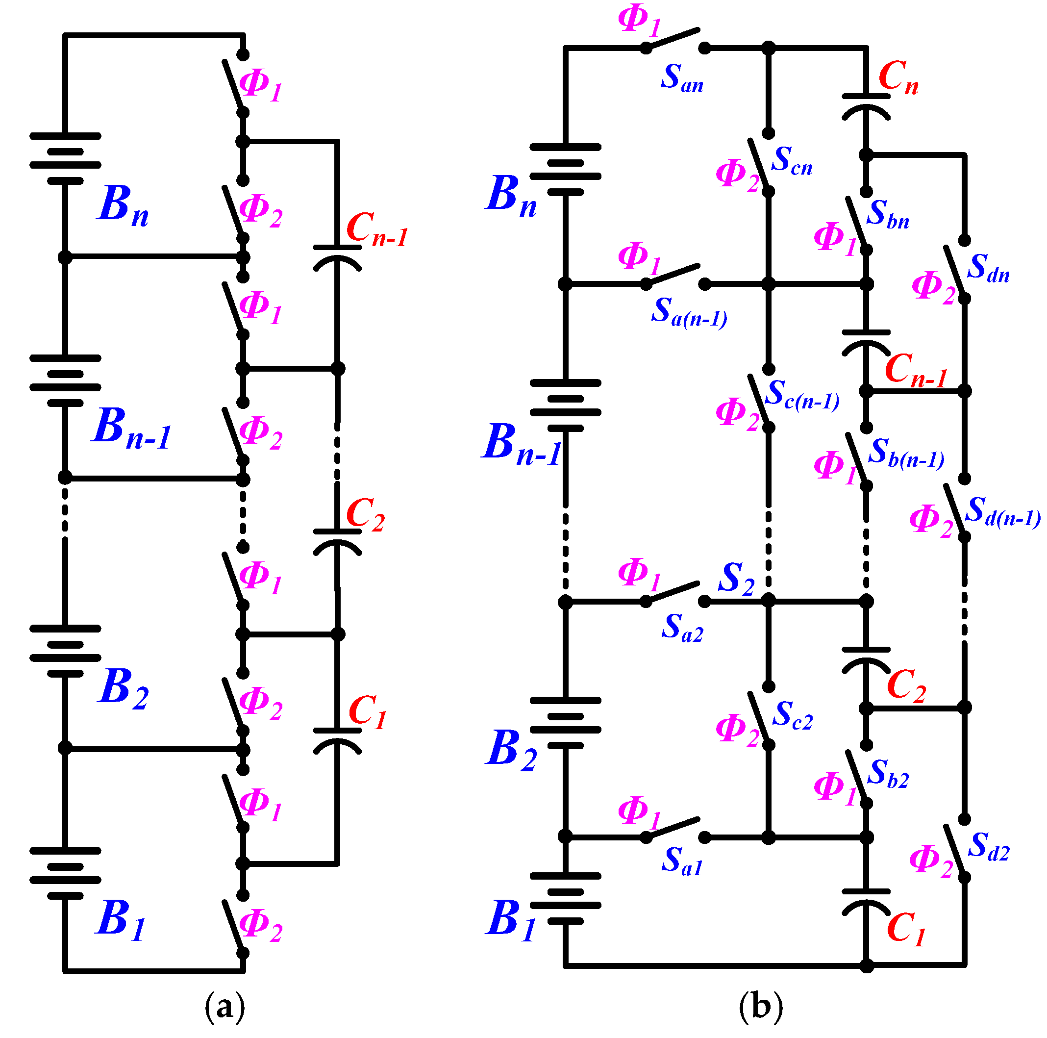
10]. It means SC voltage equalizer can be designed with smaller size and lower cost. The conventional structure of SC voltage equalizers is shown in Figure 1a [11]. Its resonant versions are also developed in [12] for high efficiency applications. In this structure, the charge flows just in two adjacent battery cells. The balancing speed is therefore limited, which makes this structure difficult to apply in those series strings with larger numbers of cells. The double-tiered version of this structure is presented in [13] to improve this balancing speed. However, this novel method does not fundamentally solve the problem that charge cannot be transferred from the highest voltage cell to the lowest one directly.
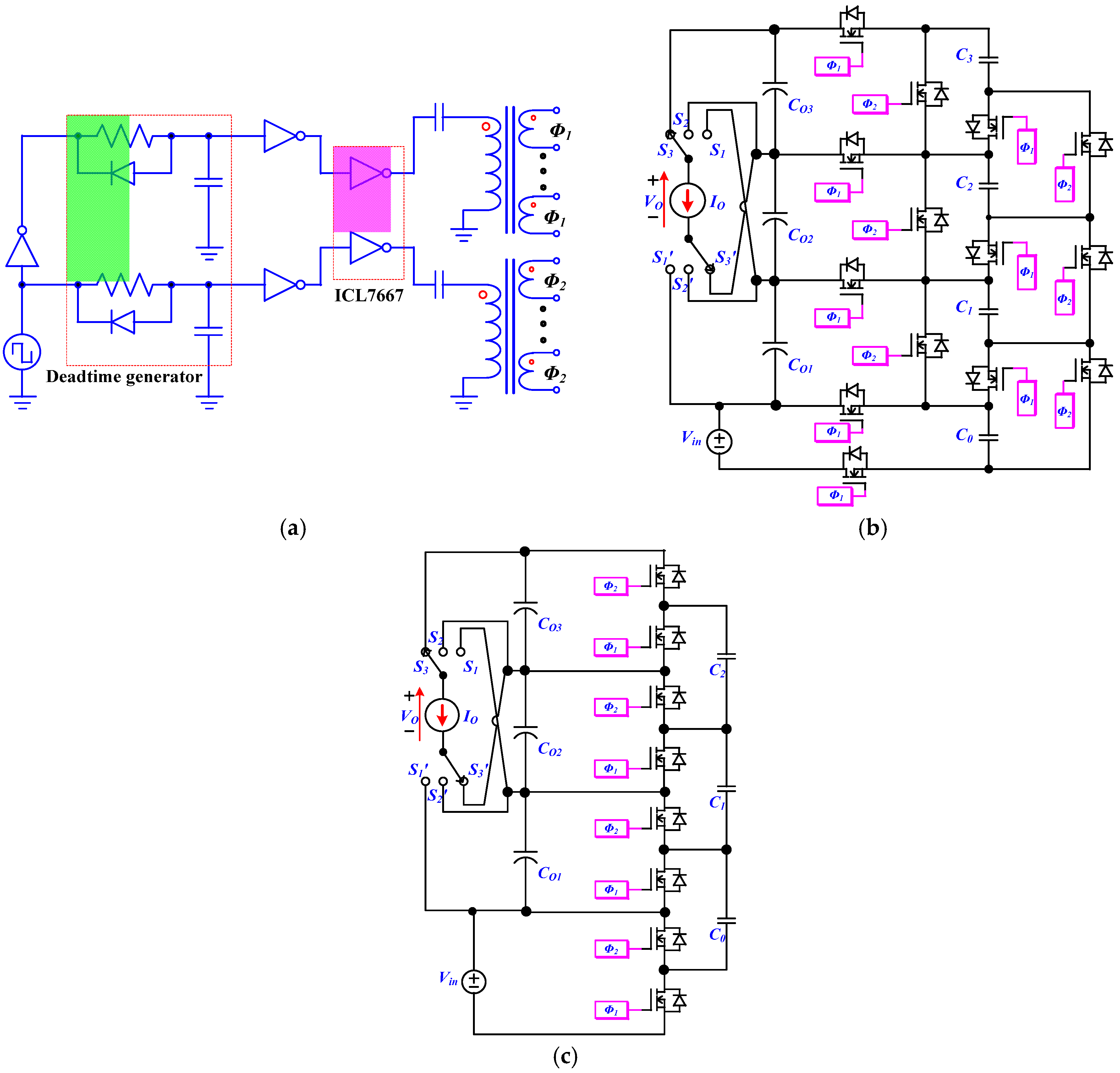
In this paper, a novel design concept of SC voltage equalization system is presented to overcome the problem existed in the conventional structure (see Figure 1a). The structure of the proposed system is shown in Figure 1b, which is also developed based on the two-phase SC technique. All switches are therefore controlled by just a pair of complementary pulse signals with fixed frequency and duty ratio. These features are very similar to the previous work presented in [14] but with different topology and circuit configuration. The main advantage of the proposed SC voltage equalizer compared to the conventional one is that charge can be transferred from any one battery cell with higher voltage to any one lower voltage cell directly. It means the voltage balancing speed could be significantly higher than the conventional one and makes the SC voltage balancing technique usable for those battery strings with a larger number of series cells.

2. Proposed Automatic Switched-Capacitor Voltage Equalizer of Battery Strings

2.1. Circuit Configuration

As shown in Figure 1b, the proposed voltage equalization system is designed based on the switched capacitor technique. It means bulky magnetic components are absent in the power conversion system. For a battery/EDLC pack formed by n series cells, n switched capacitors and 4n − 3 switches are required. There are two clock phases Φ1 and Φ2 as indicated in Figure 2, for which the switch will be closed. The process, charge transferred from the higher voltage cells to the lower ones, is completed by alternatively switching the capacitors from in-series to in-parallel and vice versa. Based on the assumptions that there are the same on-resistance rS for all switches and the same equivalent series resistance (ESR) rC for all capacitors employed in the system, the circuit is also reconfigured into two capacitive networks as shown in Figure 3a–c separately in the two clock phases, where Rk and Ri are the total resistance of the capacitive loops and both are equal the sum of the ESR of one capacitor and the on-resistance of three switches, i.e., Ri = Rk = rC + 3rS.
In the stable state, two operation manners are found in phase Φ1. For the case that the initial voltage across the capacitor Ck is higher than that for battery cell Bk, the capacitor will discharge to the cell Bk causing the capacitor voltage decrease as shown in Figure 3a. Conversely, the capacitor will be charged by the battery cell Bk when its initial voltage is lower than the later, as shown in Figure 3b. For the phase Φ2, all capacitors are connected in parallel and charge flows form the capacitors with higher voltage to the lower ones as shown in Figure 3c.

2.2. Charge Transferred from Capacitor to Battery for Φ1

As mentioned before, charge will flow from the capacitor with higher initial voltage to the battery cell causing the voltage across the capacitor Ck to decrease from its maximum value to the minimum value. The voltage across the battery cell could be seen as constant based on the premise that the capacity of the cell Bk is far larger than that for Ck. The variation of the capacitor current and voltage can be therefore expressed by:
I C k ( t ) = I C k _ max e t R k C k = V C k _ max V B k R k e t R k C k
V C k ( t ) = V C k _ max ( V C k _ max V B k ) ( 1 e t R k C k )
The minimum voltage across the capacitor is obtained at the end of the discharge process. It will be equal to the battery cell’s voltage when the RkCk constant is far small than the charging duration T1 as shown by Figure 4a. Otherwise, the minimum voltage will be higher than the voltage across the battery cell as shown in Figure 4b.
During the whole discharging process, the amount of charge and energy released by the capacitor are given by:
Q C k = C k ( V C k _ max V C k _ min )
E C k = C k 2 ( V C k _ max 2 V C k _ min 2 )
All charge released by the capacitor Ck will be transferred to Bk. However, the energy absorbed by the battery cell is not the same as that released by Ck, and is expressed as:
E B k = C k V B k ( V C k _ max V C k _ min )
The energy loss can be therefore derived from Equations (4) and (5), and is given by:
E loss ( k ) = C k 2 [ ( V C k _ max V B k ) 2 ( V C k _ min V B k ) 2 ]

2.3. Charge Transferred from Battery to Capacitor for Φ1

In the phase Φ1, when the battery cell’s voltage is higher than the voltage across the corresponding capacitor, charge will flow from the cell Bi to the capacitor and Ci is charged. The capacitor voltage rises from its minimum value to the maximum value. The variation of the capacitor current and voltage during the charging process can be expressed by:
I C i ( t ) = I C i _ max e t R i C i = V B i - V C i _ min R i e t R i C i
V C i ( t ) = V C i _ min + ( V B i V C i _ min ) ( 1 e t R i C i )
The maximum voltage across the capacitor is also obtained at the end of the charging process. Similar with the discharging process analyzed before, the maximum capacitor voltage will be equal to the battery cell’s voltage when the RiCi constant is far small than the charging duration T1 as shown by Figure 5a. Otherwise, the maximum voltage will be lower than the voltage across the battery cell as shown in Figure 5b.
The amount of charge and energy released by the battery cell Bi during the charging process are given by:
Q B i = C i ( V C i _ max V C i _ min )
E B i = C i V B i ( V C i _ max V C i _ min )
Similarly, all of charge will be transferred to Ci and the incremental energy for the capacitor is expressed as:
E C i = C i 2 ( V C i _ max 2 V C i _ min 2 )
According to the Equations (10) and (11), the energy loss the charging process is given as:
E l o s s ( i ) = C i 2 [ ( V B i V C i _ min ) 2 ( V B i V C i _ max ) 2 ]

2.4. Capacitor Balancing Analysis for Φ2

During the phase Φ2, all capacitors with different voltages are connected in parallel though switches as shown in Figure 3c. Charge flows from the capacitors with the higher voltage to the ones with lower voltage causing the higher capacitor voltages to decrease and the lower ones to increase gradually as shown in Figure 6. In the case that the period of the phase Φ2 is far longer than the all RC constants of the capacitive network, all capacitor voltages would change to the same level at the end of this duration.
Taking the capacitors Ci with higher initial voltage and Ck with lower initial voltage as example, the capacitor voltage VCi decreases from its maximum value to the minimum whereas VCk changes in the opposite manner. The amounts of charge absorbed by Ck and released from Ci are also QCk and QCi, respectively, as given by Equations (3) and (9). Additionally, the energy decrease in the capacitor Ci is the same as that of it absorbed in the phase Φ1 as given in Equation (11). And the incremental energy in Ck is the same as that of it released in the phase Φ1 as given in Equation (4).

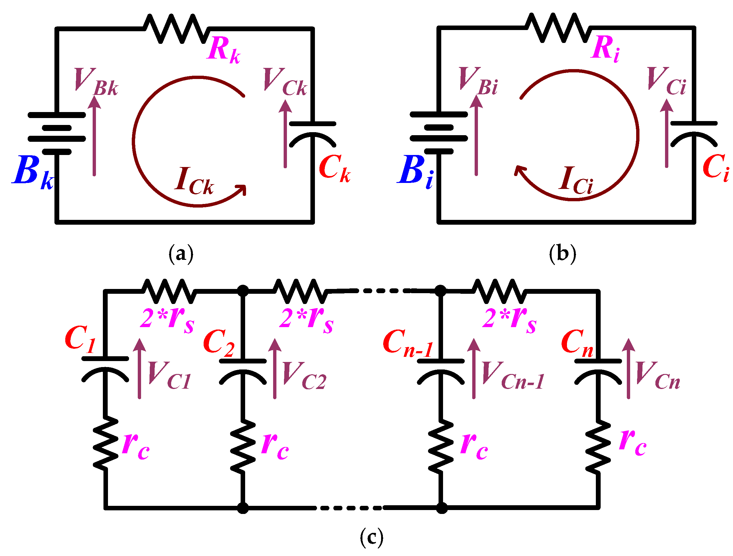
3. Modeling of Proposed SC Voltage Equalizer

In order to facilitate analysis, the following assumptions are made: (i) the on-resistance of switches is so small as compared to the ESR of capacitors that it could be neglected or regarded as a part of the ESR of capacitors; (ii) all capacitors employed in the system have the same capacitance C and ESR rC. In this case, the state circuit of Figure 3c is redrawn in Figure 7a.
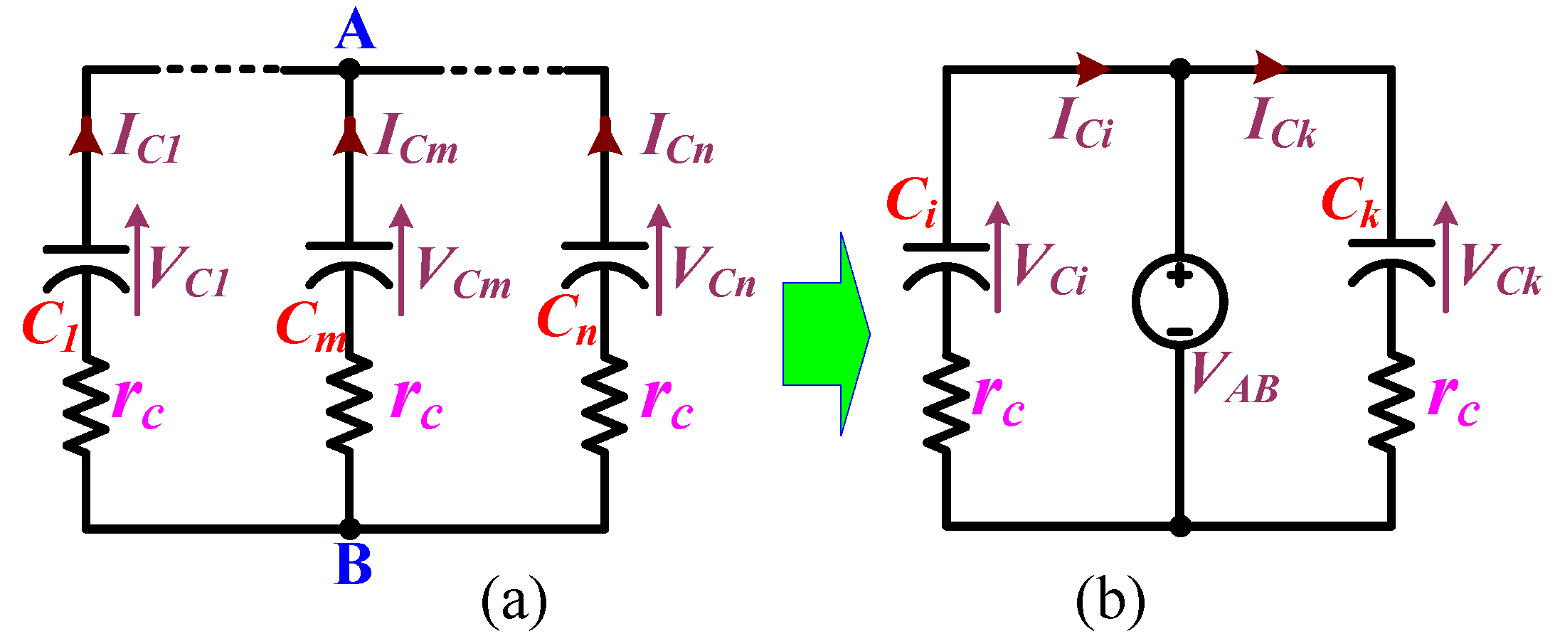
The voltage difference between the points A and B can be expressed as:
V A B = 1 n m = 1 n ( V C m + r C I C m )
By using Kirchhoff’s current law (KCL) at the point of A, the KCL equation could be obtained as given by:
1 n m = 1 n I C m = 0
When the KCL Equation (14) is substituted into Equation (13), the voltage VAB could be further expressed as:
V A B = 1 n m = 1 n V C m = 1 n C m = 1 n q C m = q total n C
where qCm is the amount of charge stored in the capacitor Cm and 
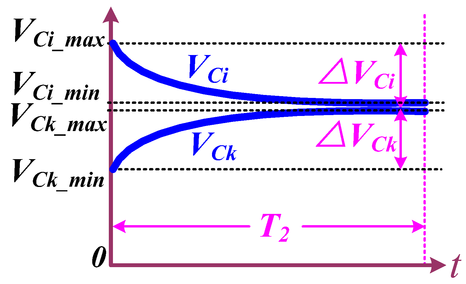
qtotal is the total amount of charge of all capacitors. During the whole capacitor balancing process of the phase Φ2, though charge is transferred from capacitors with the higher voltage to those with the lower voltage, the total charge is constant and the voltage VAB is therefore can be seen as a constant voltage source. As a result, the equivalent circuit for the phase Φ2 is derived form above analysis as shown in Figure 7b.
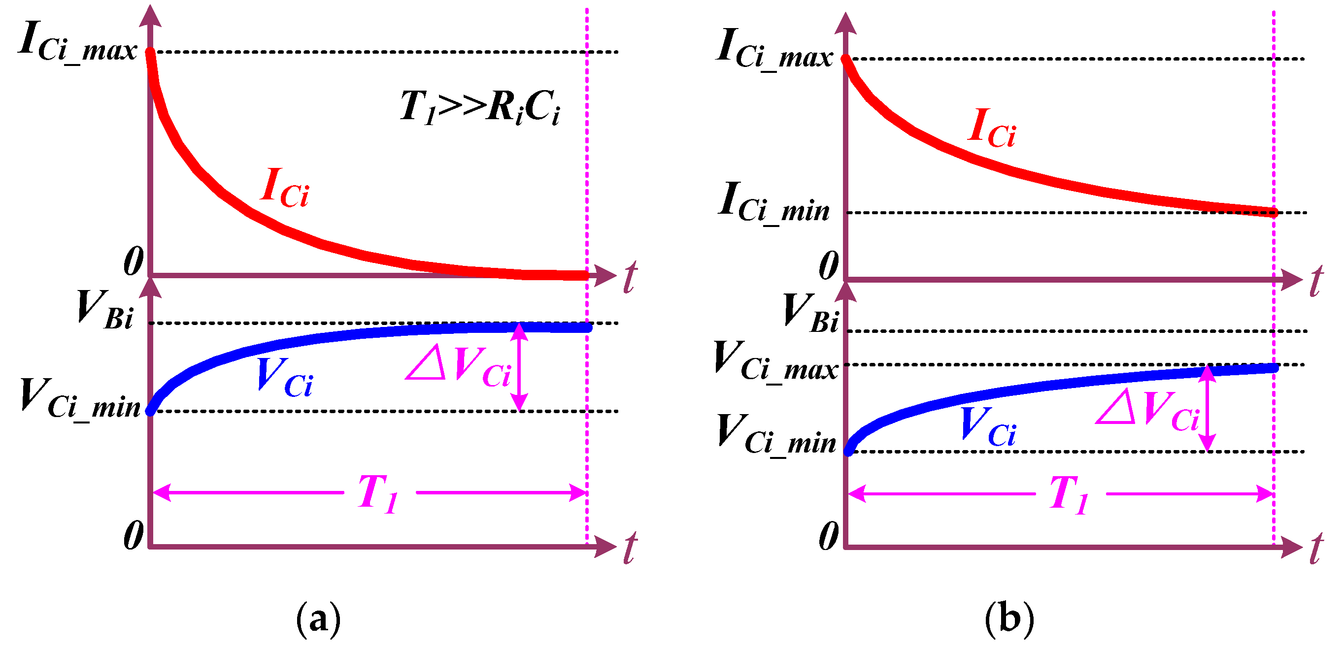
Based on the assumptions made before, the variation of the voltage across the capacitor Ck, which corresponds to the battery cell Bk with lower voltage, can be expressed as:
Φ 1 :   V C k ( t ) = V C k _ max ( V C k _ max V B k ) ( 1 e t r C C )
Φ 2 :   V C k ( t ) = V C k _ min + ( V A B V C k _ min ) ( 1 e t r C C )
Considering the minimum and maximum values of the capacitor voltage VCk are obtained at the end of the periods of the phases Φ1 and Φ2, respectively, the relationship of the voltages VBk and VAB can be derived as:
V A B = V B k + I B k R B k
where IBk is the average current flowing into the battery cell Bk and RBk is the equivalent resistance of the switched capacitor power conversion circuit between VBk and VAB. They are expressed as:
I B k = f S C ( V C k _ max - V C k _ min )
R B k = 1 e 1 f S r C C f S C ( 1 e T 1 r C C ) ( 1 e T 2 r C C )
where f S is the switching frequency, i.e., f S = 1 / T S .
Similarly, the variation of the voltage across the capacitor Ci, which corresponds to the battery cell Bi with higher voltage, can be expressed as:
Φ 1 :   V C i ( t ) = V C i _ min + ( V B i V C i _ min ) ( 1 e t r C C )
Φ 2 :   V C i ( t ) = V C i _ max ( V C i _ max V A B ) ( 1 e t r C C )
The maximum and minimum capacitor voltages are obtained at the end of the periods of the phases Φ1 and Φ2, respectively, the relationship of the voltages VBi and VAB can be therefore expressed by:
V A B = V B i - I B i R B i
where IBi is the average current flowing out of the battery cell Bi and RBi is the equivalent resistance between VBk and VAB. They are given as:
I B i = f S C ( V C i _ max - V C i _ min )
R B i = 1 e 1 f S r C C f S C ( 1 e T 1 r C C ) ( 1 e T 2 r C C )
It can be seen from the Equations (20) and (25) that there is the same equivalent resistance between the constant voltage source VAB and any one battery cell, regards of the cell Bi with higher voltage or the cell Bk with lower voltage.
As well known, an SC power conversion circuits can be equivalent to a combination of an ideal DC transformer and an equivalent resistance [15,16,17]. The model of the proposed automatic voltage equalizer with battery string is derived based on the above analysis, as depicted in Figure 8. The turns of the ideal multi-winding DC transformer are the same. The value of the equivalent resistor RB is the same as RBk and RBi given in Equations (20) and (25). In the case that ignoring the impact of parasitic resistance, the equivalent resistor RB could be simplified as given by:
R B = 1 f S C

4 Comparison of Proposed Switched-Capacitor Voltage Equalizer with Conventional One

4.1. Switch Stress Comparison

For the switch stress, all of switches in the conventional one share the same voltage stress VB which is the battery’s cell voltage. The same switch stress is also found across all switches Sbi, Sci and Sdi (i = 2, …, n) in the proposed voltage equalizer (see Figure 1b). For the switch Saj (j = 1, 2, …, n), it withstands the blocking voltage (j − 1)VB. It means the blocking voltage increases along with the increase of the number j and the maximum switch stress (n − 1)VB is found across the switch San. Considering the cell voltage VB is usually not higher than 4 V for lithium batteries or 3 V for EDLCs, there is no difficulty to select appropriate transistors to meet the requirement of switch stresses.
For the conventional SC voltage equalizer, a switch is connected to the midpoint tap of two nearby switched capacitors when it is ON. We denote that the capacitor current is positive during charging process whereas it is negative for discharging process. The switch current is therefore the algebraic difference of the two capacitors’ charging or discharging current, i.e., (iCk + 1 − iCk). The same current is also found for the group of switches Saj in the proposed equalization system. For the switch Sbj, its current is the same as the capacitor current iCj. Additionally, the currents flowing though Scj and Sdj are the same and both equal to the algebraic sum of all capacitor currents iCk (k = 1, 2, …, j − 1). The blocking current of each switch can be therefore derived from the maximum charging and discharging currents of corresponding switched capacitors.

4.2. Model Comparison

Using the same modeling method described in the Section 3 for the voltage equalizer of Figure 1a, its model is obtained as shown in Figure 9. The equivalent resistance RB is the same as that for the model of the proposed one as shown in Figure 8 with the premise that there are same capacitors and switching frequency in the two voltage equalizers. It could be seen clearly that there are multiple ideal DC transformers with two windings in the model of Figure 9. The two windings of each transformer are connected with the two adjacent battery cells. In contrast, there is only one ideal DC transformer with multiple windings in the model of the proposed voltage equalizer as shown in Figure 8.
Comparing the two models, the equivalent resistance between two adjacent battery/EDLC cells is 2RB is Figure 8 whereas is RB in Figure 9. It means the charge-balancing speed of the conventional equalizer (see Figure 1a) is twice that of the proposed one. However, when charge is need to transfer from the battery cell Bi with higher initial voltage to Bk with lower initial voltage, the speed is no longer the same as that for two adjacent cells. In order to facilitate analysis, assuming the cell number k is larger than i, i.e., k > i. It could be obtained from the model of Figure 9 that the equivalent resistance between the two cells Bk and Bi is (k − i)RB, whereas the equivalent resistance 2RB is still found between Bk and Bi in the model of Figure 8.
Hence, the balancing speed of the conventional equalizer is directly related to the interval between the cells Bk and Bi. The farther the interval, the slower the speed is. For the proposed voltage equalizer, however, the balancing speed is independent of the cells’ interval.
Assuming the same power (Vin × Iin) flows into the cell-port of Bi and the cell-port of Bk is configured as the output terminal in the two compared systems, it could be found that the power loss during the transferring process is (k − i)RBIin2 for the conventional equalizer whereas 2RBIin2 for the proposed one. Clearly, the power conversion efficiency of the proposed voltage equalizer is higher than that for the conventional one when the interval (k − i) is larger than 2.
Summing up the above analysis, the conventional voltage equalizer of Figure 1a is more suitable for the battery/EDLC strings including two series cells. For strings composed by a large number of series cells, the proposed voltage equalizer is superior to the conventional one in the aspect of balancing speed and power conversion efficiency. The larger the number of series battery/EDLC cells, the more obvious the superiority is.

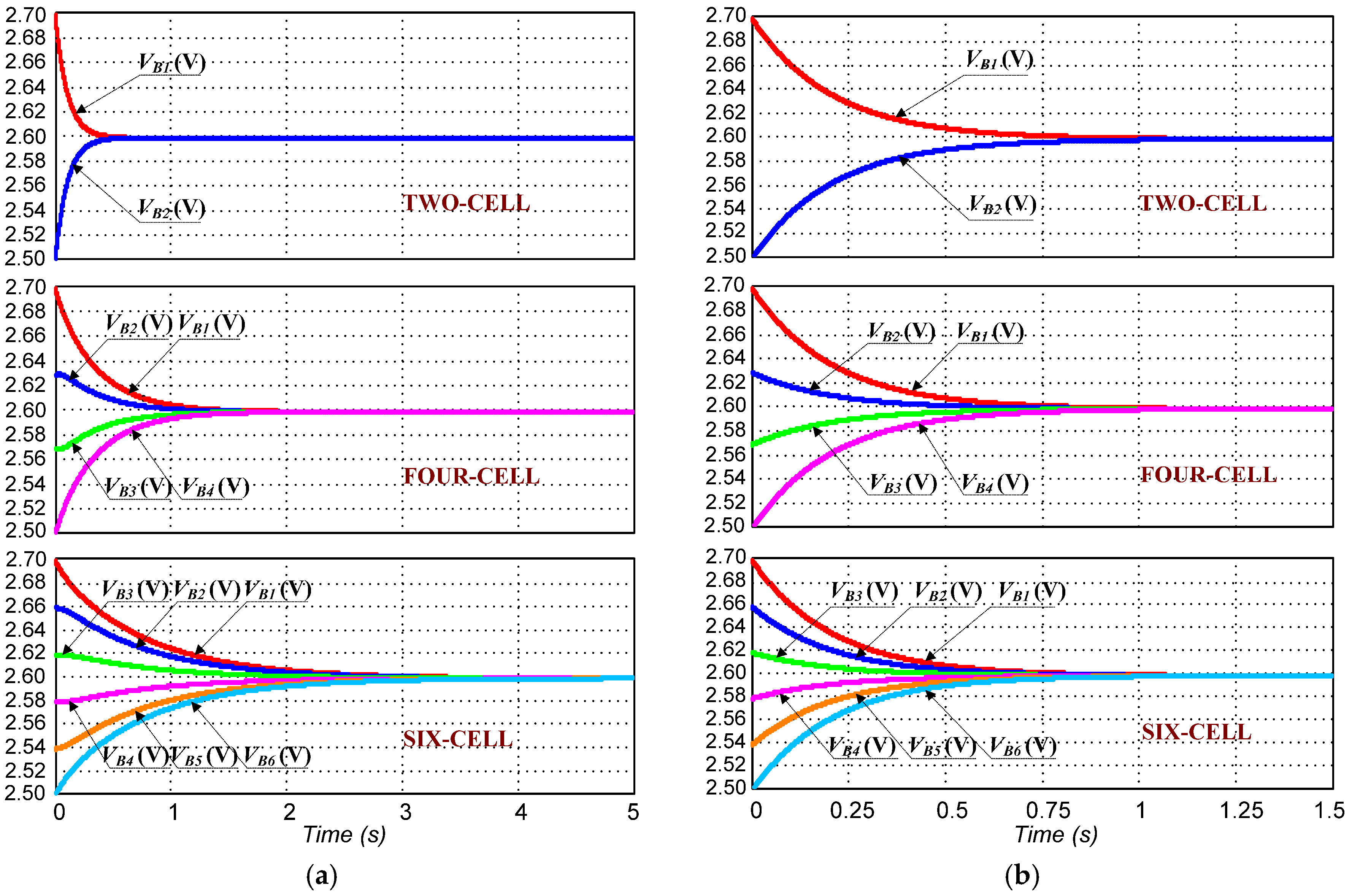
4.3. Simulation Comparison

Figure 10a,b shows the simulation cell-voltage waveforms of the balancing process for two-, four- and six-cell EDLC strings with the conventional and proposed SC voltage equalizers, respectively.
The value of each switched capacitor employed in the both simulation equalization circuits is 220 μF. The two systems both operate at 22 kHz switching frequency and every one switching cycle is evenly divided by the two phases Φ1 and Φ2. Capacitors with 1 F capacitance and different initial voltages are used as cells. For the two-cell string, the initial voltages of cells are 2.7 V and 2.5 V. It could be seen from the upper of Figure 10a that the voltage gap between the two cells changes from 0.2 V to zero for about 0.5 s with the conventional equalizer, which is shorter than that with proposed one, 1.1 s given in the upper of Figure 10b. For the four-cell system with initial cell voltages (2.5 V 2.57 V 2.63 V 2.7 V), the balancing process consumes about 1.9 s for the conventional equalizer while 1.1 s for the proposed one, as shown in the middles of Figure 10a,b. With initial cell voltages (2.5 V 2.54 V 2.58 V 2.62 V 2.66 V 2.7 V), the equalization process for six-cell is given in the lower of both subfigures. It shows that the balancing time is more than 4.5 s for the conventional equalizer while still about 1.1 s for the proposed one.
Comparing the three balancing processes given in both Figure 10a,b, it could be seen that the balancing time increases significantly along with the increase of the number of series EDLC cells for the conventional SC voltage equalizer. For the proposed SC equalizer, however, the balancing duration is almost independent from the number of the series cells. Thus, the same conclusions that the proposed voltage equalizer is superior to the conventional one for the multi-cell string and the latter is more suitable for two-cell system are found in both model comparison and simulation results.

5. Experimental Verification

5.1. Prototypes and Characteristics Test

Prototypes of both the conventional and proposed SC automatic voltage equalizers for four-cell strings have been built. All switches are implemented by the same MOSFETs with on-resistance 2.8 mΩ and all switched capacitors are implemented by 220 μF/11 mΩ electrolytic capacitors.
A pair of complementary gate signals with 22 kHz switching frequency and fixed duty ratio as well as reasonable dead-time are generated by the driver circuit as given in Figure 11a. At first, the two prototypes are configured as Figure 11b,c, respectively. The lowest cell-port of both prototypes is connected with a voltage source Vin = 3 V as input power and other cell-ports are connected with 1000 μF electrolytic capacitors. As load, a current source IO is connected with one of three combined switches (S1_S1, S2_S2, S3_S3’). When the combined switch S3_S3 is turned ON, a constant current load IO = 1 A is connected to the highest cell-port in both test systems and gate signals as well as currents flowing though switched capacitors are obtained as shown in Figure 12.
Because of the effect of ESL in capacitors, the current waveforms are smooth and increase from zero at the beginning of each phase, which contributes to the switching losses and EMI reductions. It could be seen from Figure 12a that there are just two switched capacitors C0 and C3 involved in the energy transfer process for the proposed equalizer. C1, C2 are idled and energy is transferred from Vin to the CO3 directly, though C0 and C3. For the conventional equalization system, energy is transferred from Vin to CO1 firstly, then to CO2 and to CO3 lastly, there is therefore no switched capacitors could be idled and their current waveforms are shown in Figure 12b.
By selecting different combined switches, different cell-ports are configured as the output terminal and been connected with the constant current load IO. When the output current is varied from 0.2 A to 3 A, the output voltages are measured as depicted in Figure 13a for the proposed equalizer and Figure 13b for the conventional one. For the SC converters with voltage conversion ratio 1:1, power is transferred from input sources to load in the form of charge. The amount of charge transferred from the input source will be totally released to load and the average input current Iin is the same as the output current IO for the two test systems because both of Iin and IO are the integration of the same charge in unit time in the case where the driving loss of switches is ignored. The power conversion efficiency has therefore the same trend with the change of output voltage, as shown in Figure 13. For the conventional SC equalizer, it could be seen from Figure 13b that the output voltage as well as the power conversion efficiency decreases along with the increase of the interval between the input cell-port and the output one. For the proposed one, however, both of the output voltage and efficiency are just related to the output current and independent from the selected output cell-port as shown in Figure 13a.
The equivalent resistances from the input cell-port to different output cell-ports are also measured for the two test systems of Figure 11b,c, as depicted in Figure 14. R0_i (i = 1, 2, 3) represents the equivalent resistance from the input terminal Vin to the selected output cell-port COi. For the conventional equalizer prototype, when i changes from 1 to 3, the equivalent resistance increases from 0.23 Ω to 0.48 Ω to 0.63 Ω, this trend is the same as the model of Figure 9 with the theoretical resistor RB = 0.2 Ω. In contrast, the equivalent resistances for the proposed equalizer prototype are basically the same for all different output cell-ports, which is also close to the model of Figure 8 with the theoretical resistor RB = 0.2 Ω.

5.2. Voltage Equalization Test for Four-Cell Electric Double-Layer Capacitor String

With different initial voltages (2.32 V 1.81 V 1.36 V 0.95 V) of four series EDLCs (2.7 V, 350 F, labeled as B1, B2, B3 and B4), the equalization processes with prototypes of the conventional and proposed SC equalizers are shown in Figure 15a,b, respectively. It depicts the equalization process continues for about 350 s for the conventional equalizer whereas 200 s for the proposed one. And all voltages change to about 1.6 V at the end. The conclusion that the voltage balancing speed of the proposed equalizer is faster than that of the conventional SC equalizer agrees with the theoretical analysis and the simulation results.

6. Conclusions

A novel voltage balancing system for series battery/EDLC strings is developed based on a two-phase SC technique in this paper. No bulky magnetic components or complex monitoring and control systems are required in the proposed voltage equalizer. The whole system is controlled by just a pair of complementary pulse signals with fixed switching frequency and fixed duty ratio of 0.5. The circuit configuration and operation principle of the proposed voltage equalizer are analyzed in detail. The model is also derived by using KVL and KCL for its state circuits. The same conclusions that the conventional SC voltage equalizer is more suitable for two-cell battery/EDLC strings than the proposed one and the latter is superior to the conventional one for the multi-cell battery strings are found in both model comparison and simulation results. Experimental results on a four-cell EDLC string indicate that the proposed voltage balancing circuit has outstanding voltage equalization performance with a simple control method. The proposed voltage balancing system therefore could be used widely for high stacks of series battery or EDLC strings. Of course, the main drawback of the proposed balancing circuit is that a large number of switches are employed.

Acknowledgments

The authors grateful acknowledge the financial support in part by the Innovation and Technology Fund of Hong Kong ITC and JL Ecopro Tech. Ltd. under Project UIM245 and in part by The Hong Kong Polytechnic University under Project H-ZG1X.

Author Contributions

Yuanmao Ye developed the circuit, hardware prototyping and conducted the test. He also conducted the simulation and results analysis. Ka Wai Eric Cheng was responsible for the switched-capacitor background theory. He also provided the guidance and supervision of the study.

Conflicts of Interest

The authors declare no conflict of interest.

References

  1. Chatzakis, J.; Kalaitzakis, K.; Voulgaris, N.C.; Manias, S.N. Designing a new generalized battery management system. IEEE Trans. Ind. Electron. 2003, 50, 990–999. [Google Scholar] [CrossRef]
  2. Kutkut, N.H.; Wiegman, H.L.N.; Divan, D.M.; Novotny, D.W. Design considerations for charge equalization of an electric vehicle battery system. IEEE Trans. Ind. Appl. 1999, 35, 28–35. [Google Scholar] [CrossRef]
  3. Zhang, D.-H.; Zhu, G.R.; He, S.J.; Qiu, S.; Ma, Y.; Wu, Q.M.; Chen, W. Balancing Control Strategy for Li-Ion Batteries String Based on Dynamic Balanced Point. Energies 2015, 8, 1830–1847. [Google Scholar] [CrossRef]
  4. Cheng, K.W.E.; Divakar, B.P.; Wu, H.J.; Ding, K.; Ho, F.H. Battery-Management System (BMS) and SOC Development for Electrical Vehicles. IEEE Trans. Veh. Technol. 2011, 60, 76–88. [Google Scholar] [CrossRef]
  5. Ongaro, F.; Mattavelli, P. Li-Ion Battery-Supercapacitor Hybrid Storage System for a Long Lifetime, Photovoltaic-Based Wireless Sensor Network. IEEE Trans. Power Electron. 2012, 27, 3944–3952. [Google Scholar] [CrossRef]
  6. Uno, M.; Tanaka, K. Single-Switch Multioutput Charger Using Voltage Multiplier for Series-Connected Lithium-Ion Battery/Supercapacitor Equalization. IEEE Trans. Ind. Electron. 2013, 60, 3227–3239. [Google Scholar] [CrossRef]
  7. Guo, X.W.; Kang, L.Y.; Huang, Z.Z.; Yao, Y.; Yang, H.Z. Research on a Novel Power Inductor-Based Bidirectional Lossless Equalization Circuit for Series-Connected Battery Packs. Energies 2015, 8, 5555–5576. [Google Scholar] [CrossRef]
  8. Cao, J.; Schofield, N.; Emadi, A. Battery balancing methods: A comprehensive review. In Proceedings of the IEEE Vehicular Power and Propulsion Conference, Harbin, China, 3–5 September 2008; pp. 1–6.
  9. Ye, Y.M.; Cheng, K.W.E. Level-Shifting Multiple-Input Switched-Capacitor Voltage-Copier. IEEE Trans. Power Electron. 2012, 27, 828–837. [Google Scholar]
  10. Xu, C.D.; Cheng, K.W.E. A Switched Capacitor Based AC/DC Resonant Converter for High Frequency AC Power Generation. Energies 2015, 8, 10842–10860. [Google Scholar] [CrossRef]
  11. Pascual, C.; Krein, P.T. Switched capacitor system for automatic series battery equalization. In Proceedings of the Applied Power Electronics Conference, Atlanta, GA, USA, 23–27 February 1997; pp. 848–854.
  12. Ye, Y.M.; Cheng, K.W.E.; Yeung, Y.P.B. Zero-Current Switching Switched-Capacitor Zero-Voltage-Gap Automatic Equalization System for Series Battery String. IEEE Trans. Power Electron. 2012, 27, 3234–3242. [Google Scholar]
  13. Baughman, A.C.; Ferdowsi, M. Double-Tiered Switched-Capacitor Battery Charge Equalization Technique. IEEE Trans. Ind. Electron. 2008, 55, 2277–2285. [Google Scholar] [CrossRef]
  14. Ye, Y.M.; Cheng, K.W.E. Modeling and Analysis of Series-Parallel Switched-Capacitor Voltage Equalizer for Battery/Supercapacitor Strings. IEEE J. Emerg. Sel. Top. Power Electron. 2015, 3, 977–983. [Google Scholar] [CrossRef]
  15. Ye, Y.-M.; Cheng, K.W.E. Multi-input voltage-summation converter based on switched-capacitor. IET Power Electron. 2013, 6, 1909–1916. [Google Scholar]
  16. Ye, Y.-M.; Cheng, K.W.E. Voltage-Gap Modeling Method for Single-Stage Switched-Capacitor Converters. IEEE J. Emerg. Sel. Top. Power Electron. 2014, 2, 808–813. [Google Scholar] [CrossRef]
  17. Makowski, M.S.; Maksimovic, D. Performance limits of switched capacitor DC-DC converters. In Proceedings of the Power Electronics Special Conference, Atlanta, GA, USA, 18–22 June 1995; pp. 1215–1221.
Figure 1. Switched-capacitor (SC) voltage equalizer of battery strings: (a) conventional version; and (b) proposed version.
Energies 09 00138 g001
Figure 2. Time slots of the proposed voltage equalization system.
Energies 09 00138 g002
Figure 3. State circuits of the proposed voltage equalization system: (a) during phase Φ1 when VBk < VCk; (b) during phase Φ1 when VBk > VCk; (c) during phase Φ2.
Energies 09 00138 g003
Figure 4. Capacitor current and voltage waveforms during the discharging process: (a) T1 is far larger than RkCk; (b) T1 is not far larger than RkCk.
Energies 09 00138 g004
Figure 5. Capacitor current and voltage waveforms during the charging process: (a) T1 is far larger than RkCk; (b) T1 is not far larger than RkCk.
Energies 09 00138 g005
Figure 6. Capacitor voltage waveform for the phase Φ2.
Energies 09 00138 g006
Figure 7. (a) Modified state circuit; and (b) equivalent circuit for the phase Φ2.
Energies 09 00138 g007
Figure 8. Model of the proposed voltage equalizer.
Energies 09 00138 g008
Figure 9. Model of the voltage equalizer in Figure 1a.
Energies 09 00138 g009
Figure 10. Simulation waveforms of the balancing process: (a) conventional one; (b) proposed one.
Energies 09 00138 g010
Figure 11. Gate driver circuit and test systems of both the conventional and proposed SC equalizers: (a) gate driver circuit of switches; (b) test system of the proposed equalizer; and (c) test system of the conventional SC equalizer.
Energies 09 00138 g011
Figure 12. Gate signals and currents waveforms with ON switch S3_S3: (a) waveforms of the proposed equalizer; and (b) waveforms of the conventional equalizer.
Energies 09 00138 g012
Figure 13. Measured output voltage and efficiency with different output cell-ports: (a) the test system of Figure 11b; and (b) the test system of Figure 11c.
Energies 09 00138 g013
Figure 14. Measured equivalent resistances of the test systems of Figure 11b,c.
Energies 09 00138 g014
Figure 15. Experimental voltage waveforms of equalization test for four-series electric double-layer capacitors (EDLCs): (a) with the conventional equalizer; and (b) with the proposed equalizer.
Energies 09 00138 g015

