Article

Simplified Process for Manufacturing Macroscale Patterns to Enhance Voltage Generation by a Triboelectric Generator

Department of Mechanical and Control Engineering, Handong Global University, Pohang 558, Korea
*
Author to whom correspondence should be addressed.
Energies 2015, 8(11), 12729-12740; https://doi.org/10.3390/en81112340
Submission received: 21 September 2015 / Revised: 1 November 2015 / Accepted: 3 November 2015 / Published: 11 November 2015
(This article belongs to the Special Issue Waste Energy Harvesting)

Abstract

:
This paper proposes a simple, yet effective and affordable, manufacturing process to enhance the overall efficiency of voltage generation by a triboelectric generator (TEG) using 3D printers for energy-harvesting applications. The proposed method can be classified as macroscale surface patterning, in contrast to micro- and nanoscale patterning of TEG proposed in previous studies. Experiments were conducted using a designed test-bed system that allowed the control of external factors, such as the magnitude and frequency of the frictional force and the relative humidity, and an output voltage increase of up to 67% was obtained from a TEG with macroscale patterns that increased the surface area by 14%. The peak voltage generated by the TEG was as high as 18 V, and the addition of a designed analog circuit that uses no external power enabled storage of a DC voltage of 0.4 V. In comparison with previous methods that employ micro- or nanoscale patterns, the proposed patterning method is faster and more suitable for mass production.

1. Introduction

Recently, green technology has gained much attention because of its necessity and importance for the future of humankind. Especially, energy harvesting or energy saving technology has become a major research area in the green technology [1,2].
The triboelectric effect refers to the electrical charging of different materials because of friction occurring when the materials are rubbed or pressed together. The triboelectric effect is usually regarded as potentially hazardous, especially for MOSFET transistors and CMOS integrated circuits, because it induces an undesirable static charge that can lead to ignition in the presence of dust or volatile, flammable gases. Nevertheless, the triboelectric effect has gained much attention in recent years because of its high potential for supplying power to standalone devices and for energy-harvesting applications [3].
The principle of electricity generation by the triboelectric effect is based on the transfer of charge due to friction when different materials are rubbed or pressed [4,5,6,7,8,9,10,11,12]. When such materials are in contact charge is transferred in order to maintain electrochemical equilibrium at the interface. However, when the materials are separated, some of the bonded atoms could have extra electrons. When such electrons are released, flow of charge occurs.
Research on the triboelectric effect dates back to ancient Greece, when Thales observed that a piece of amber could attract light objects after being rubbed. Through this discovery, elektron, which means amber in Greek, emerged as the origin of electricity. Several centuries later, Otto von Gueriche developed an electrostatic generator that produced electricity with a rotating sulfur ball. This device inspired many researchers to develop different forms of electricity generators using friction. Although triboelectric machines, such as the Leiden jar, were of fundamental importance for electricity generation, they were eventually replaced by batteries and modern electric generators based on Faraday’s law.
In recent research, TEG has attracted considerable attention with the growing demand for nanopower generators and storage of mechanical energy. Noting the abundance of the triboelectric phenomena in daily life, Fan et al. [7] developed a triboelectric nanogenerator using two thin plates of Kapton and polyester (PET). They showed that the nanogenerator could produce a power density of 10.4 mW/cm3 and voltage of 3.3 V, which is suitable for LEDs, self-powered devices, and wearable electronic devices. Since the materials used are easy to fabricate, inexpensive, and scalable, such nanogenerators have considerable potential for powering mobile and personal electronics for healthcare, surveillance, and mitigation systems as well as for comfortable environments.
Therefore, owing to their simple structure and high efficiency, nanogenerators have motivated studies for further improving their efficiency and widening their application.
The primary TEG research issues that need to be addressed are enhancing the efficiency of electricity generation and simplifying the manufacturing process.
Efforts to improve the power density of a TEG have focused on adopting different materials and surface structures. Kim et al. [5] employed graphene film, owing to its ultra-high electron mobility characteristics. Lee et al. [6] constructed a porous sponge structure on the surface of aluminum film, which produced nearly 10 times more power than the bare, flat film.
Furthermore, studies on enhancing the electrical output of TEGs have focused on increasing the friction contact area. Fan et al. [7] and Yang et al. [8] adopted a MEMS photolithographic method to increase the contact area between two films. In addition, the optimal surface patterning to maximize electricity generation was investigated using cubic, linear, and pyramidal patterns; the pyramidal pattern showed the highest sensitivity and electrical output. Microscale particles were photolithographically added by Wang et al. [9] on the TEG surface in order to obtain a pattern for maximizing the friction contact area. In addition, nanoscale gold particles were assembled to the TEG surface using a specific chemical sequence to further increase the friction contact area [10,11,12].
The aforementioned studies have shown that applying micro- and nanoscale patterns and particles on the TEG surface can increase the overall friction contact area, thus enhancing the efficiency of triboelectric charging. Furthermore, TEG also showed the concept of sensitive sensors due to enhancing of triboelectric charge [13,14,15]. However, the main limitation of this technology is the cost and complexity of the manufacturing process by which micro- and nanoscale patterns are applied. Although novel, simple methods of micro-patterning exist, the patterning methods of TEG use the aforementioned complex process. Microscale patterns are obtained by photolithography, which requires a series of complicated processes such as drying, etching, mixing, degassing, and spin coating [7,8,9], while nanoscale patterns are obtained by adhering gold nanoparticles in another complicated process [13,14,15]. In addition, the production speeds of these manufacturing processes are limited.
Therefore, this paper proposes an affordable manufacturing process to enhance the overall TEG efficiency using 3D printers, which are easily accessible. The proposed method can be classified as macroscale surface patterning, in contrast to micro- and nanoscale patterning proposed in previous studies. The surface patterns are inscribed on a TEG with a mold created using a 3D printer. Since the proposed method uses a 3D printer for the patterning, it is a fast, cost-effective, and simple process for enhancing the TEG efficiency. The patterns were designed to have a square pyramid shape in order to achieve maximum power generation. A test-bed system was designed to validate the performance of the proposed system under controllable force (magnitude and frequency) and humidity. Finally, the conditions for optimal TEG operation were proposed on the basis of the experiments.
The remainder of this paper is organized as follows. Section 2 describes the process for manufacturing the macroscale patterns. Section 3 discusses the design of the test-bed system and presents the experimental analysis of the TEG. Finally, Section 4 summarizes our findings and concludes the paper.

2. Design of TEG with Macroscale Patterns

2.1. Modeling of TEG

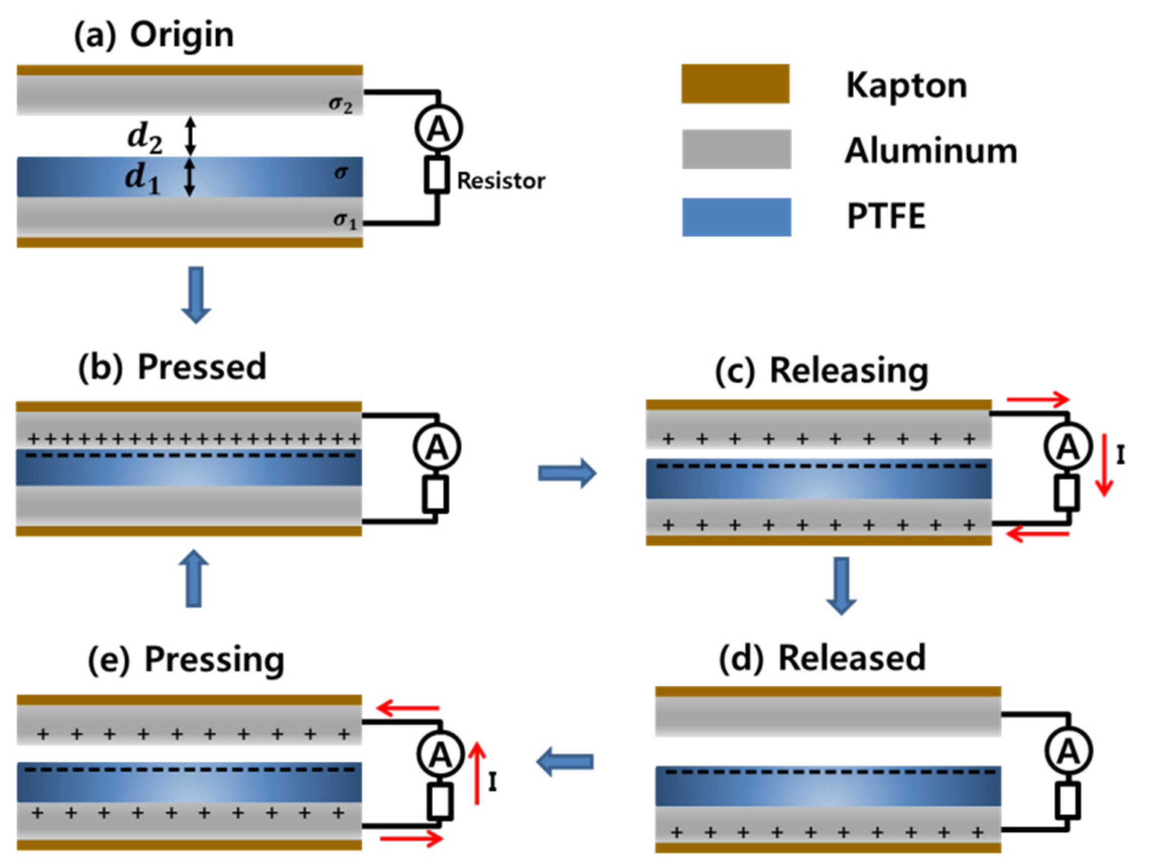
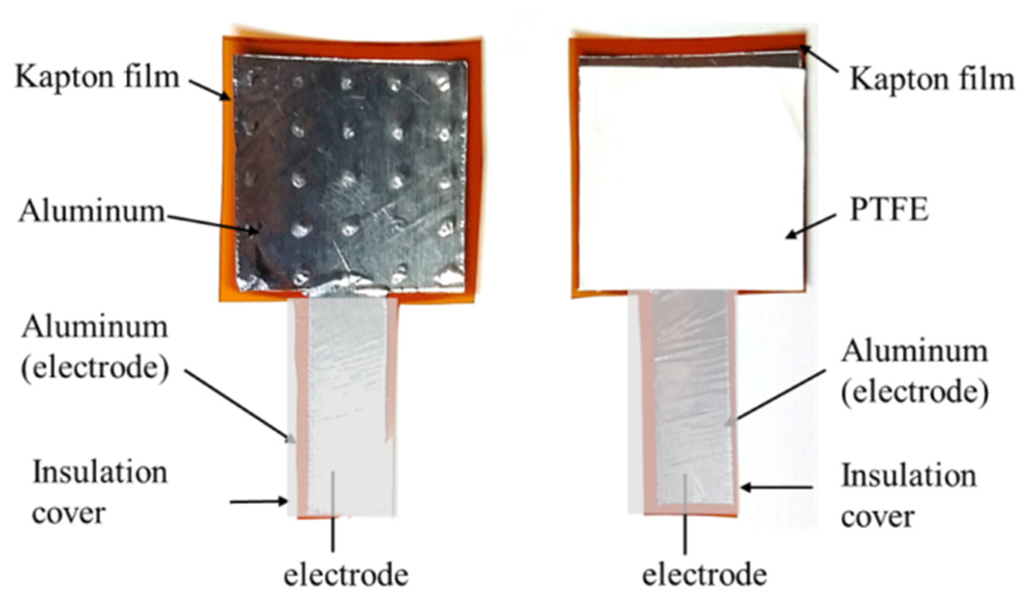
A TEG produces electricity based on the principle of the triboelectric effect, by which electric charge is induced by contacting between two different materials. In this study, the materials used to generate tribo-electric effect are aluminum and polytetrafluoroethylene (PTFE). The outer surfaces of aluminum and PTFE are coated by Kapton thin film to protect the material from any damage, as shown in Figure 1 and Figure 2. Kapton film is chosen as the coating substrate due its flexibility, light weight, and high insulation. A patch of aluminum electrode is placed between PTFE and Kapton film for the charge conduction. Aluminum electrodes are coated with insulation film to avoid the two electrodes touching each other when TEG is pressed, as shown in Figure 2.
Figure 1. Principle of electricity generation in a TEG.
Energies 08 12340 g001
Figure 2. Aluminum and PTFE films of the employed TEG.
Energies 08 12340 g002
When aluminum and PTFE surfaces are rubbed or pressed together, the electrostatic charge causes electrons to migrate such that the aluminum film becomes positively charged and the PTFE film becomes negatively charged.
The PTFE surface is charged with negative charge with density of σ and the electrode of PTFE and aluminum are charged with positive charge with density of σ1 and σ2, respectively.
At the equilibrium state, the electrical potential of the aluminum electrode (UAE) and the PTFE electrode (UPE) can be defined as [14]
U A E = U P E = 0 = σ 2 2 ε 0 d 2 + σ 2 2 ε r p ε 0 d 1 + σ 2 ε r p ε 0 d 1 σ 2 ε 0 d 2 σ 1 2 ε r p ε 0 d 2 σ 1 2 ε 0 d 2
where ε0 is the vacuum permittivity, and εrp is the relative permittivity of PTFE film (εrp = 1.93), d1 is the thickness of PTFE film (d1 = 0.2 mm), and d2 is the distance between the aluminum and PTFE.
Since the total charges are conserved, (i.e., −σσ1 = σ2) the charge density of PTFE electrode σ1 can be defined as a function of the gap distance (d2) between the PTFE and aluminum surface as [14]
σ 1 = σ 1 + d 1 d 2 × ε r p
Thus, the gap distance d2 is the principal factor that affect the distribution and flow of the electrical charges from one electrode to the other.

2.2. Method of Patterning on the TEG Surface

To enhance the electricity generation by a TEG, the overall contact surface of the TEG should be maximized. Previous studies have inscribed micro- and nanoscale patterns onto the TEG, effectively amplifying the output voltage generation at the cost of a complex and time-consuming manufacturing process. Nanoscale patterning has been accomplished photolithographically through a multi-step process that involves drying, etching, mixing, degassing, and spin coating.
Therefore, in this paper, a simple yet effective manufacturing process is proposed to enhance the TEG electricity generation using macroscale patterns inscribed on a TEG with a patterned mold created using a 3D printer. Instead of using chemicals and complicated processes, the proposed technique simply prints the patterns by pressing the mold onto the TEG surface. The ease and rapidity of this process render it suitable for mass production of TEGs. Subsequent sections of this paper describe how the proposed technique is validated. The results show that macroscale patterns can significantly amplify the voltage output of TEGs for practical applications.
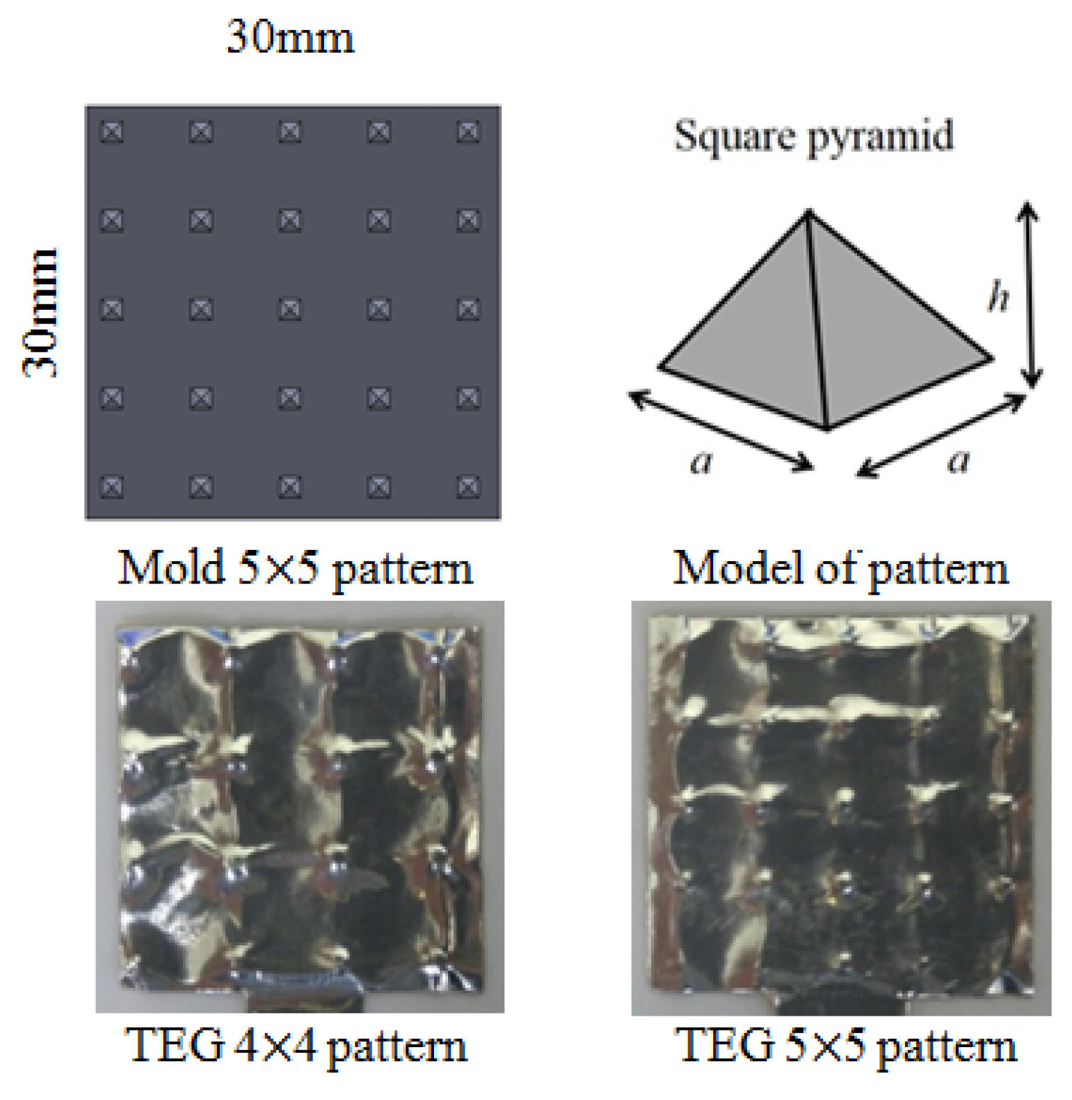
For the pattering of TEG, the mold is placed on top of the back side of the aluminum square patch and is pressed with hand to inscribe the patterns. Thus, the patterns are extrude out on the front side of aluminum surface as shown in Figure 2 and Figure 3.
Figure 3. Patterning mold made using a 3D printer (above); and the inscribed patterns on the TEG surface (below).
Energies 08 12340 g003
The mold containing the patterns was fabricated using a 3D printer. The mold was firmly pressed onto the TEG to engrave the patterns, as shown in Figure 2 and Figure 3. The patterns were designed to have a square pyramid shape with base length a and height h. Assuming that there are n patterns on the TEG with square base surface area l × l mm2, the overall surface area of the TEG is calculated as
Surface   Area = l 2 + n ( a 4 h 2 + a 2 a 2 ) ,   n < l a
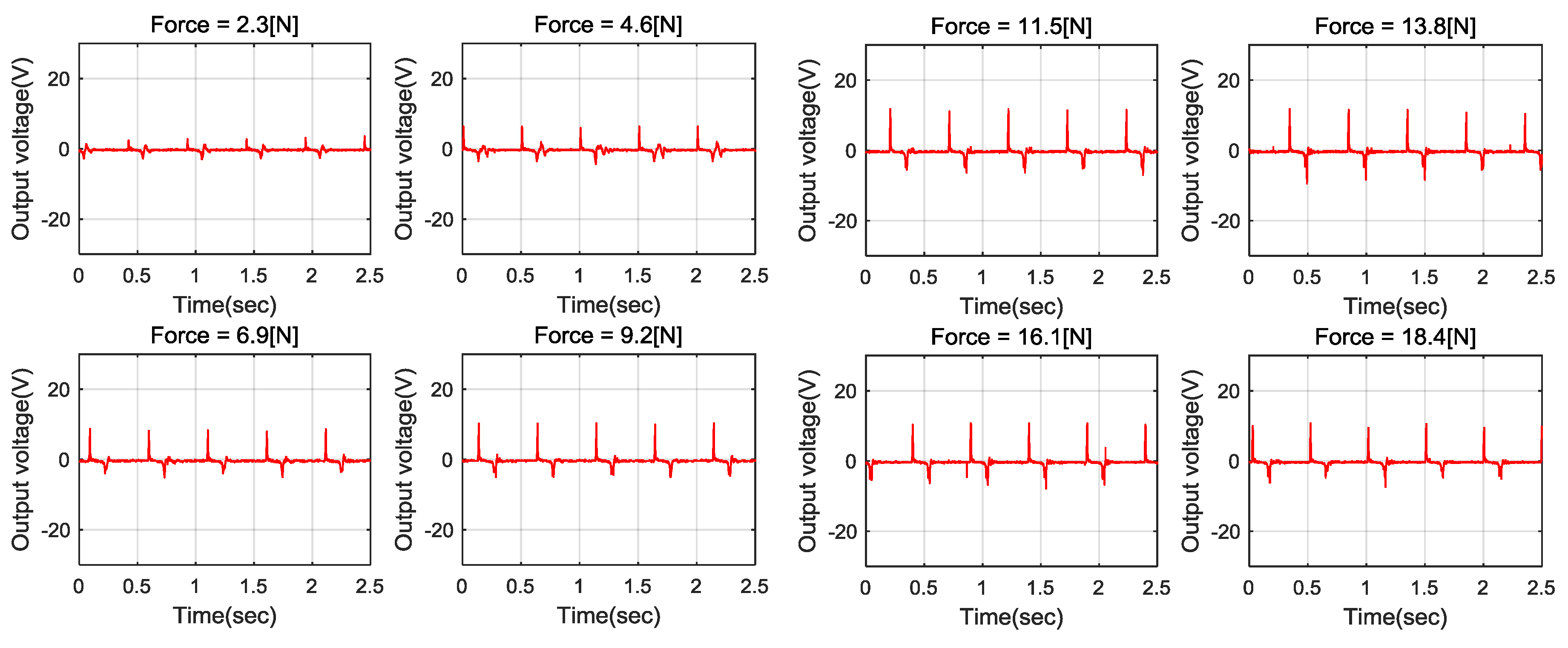
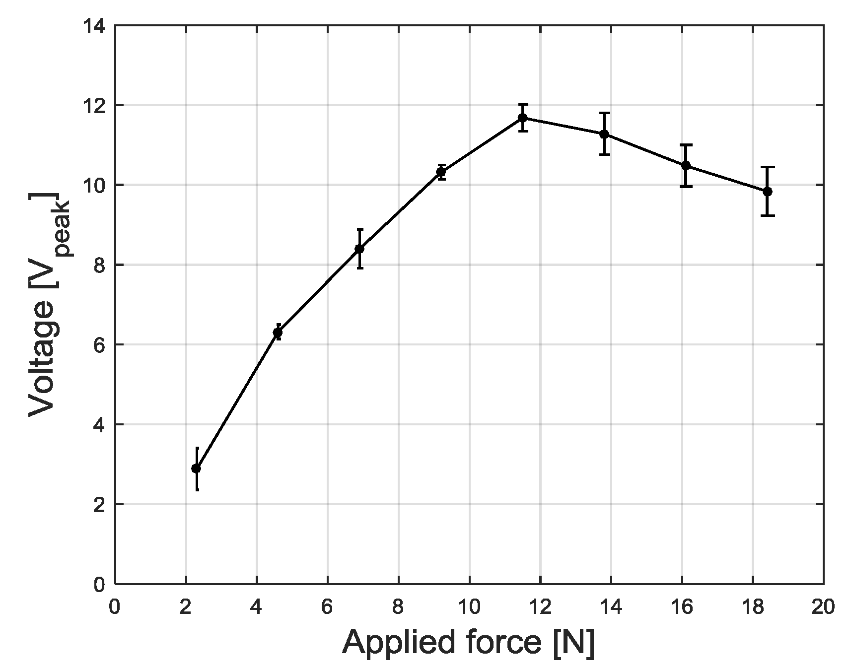
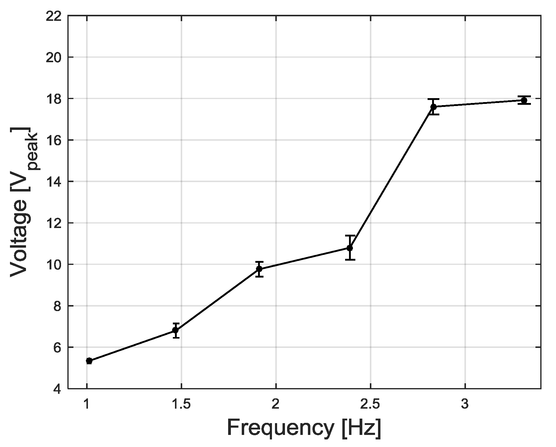
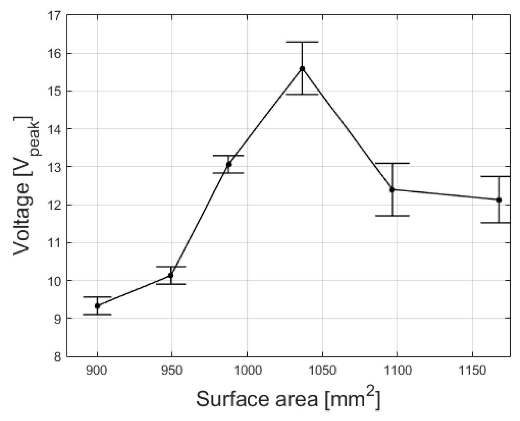
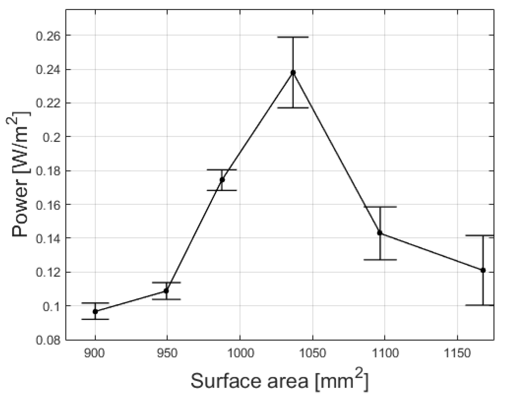
In this experiment, the size of the TEG film was set at 30 × 30 mm, and a single pattern was designed to have both base length (a) and height (h) equal to 2 mm. When n = 36, the effective contact area was increased from 900 mm2 to 1024 mm2, which is an increment of approximately 14%.

3. Analysis Results

3.1. Design of the TEG Test-Bed System

The voltage generation of a TEG is affected by several external factors, such as the magnitude and frequency of the frictional force, area of the contact surfaces, temperature, and humidity. Since multiple factors affect the TEG results, it is necessary to control these factors individually when analyzing the TEG’s properties.
Therefore, in this paper, a test-bed system was designed to control the magnitude of the compression force, the frequency of the force, and the relative humidity, as shown in Figure 4.
Figure 4. Test-bed system for analysis of the TEG’s properties.
Energies 08 12340 g004
The applied frictional force was controlled using a DC motor connected to a camshaft. The rotational motion of the DC motor is converted into a linear oscillation motion by the camshaft’s continuous frequency-controlled downward pressure on the bracket connected to the TEG, at the controlled frequency. On the weight box, pieces of metal are placed on the bracket to give various constant pressing force of 2.3 N, 4.6 N, 6.9 N and 9.2 N. In addition, bearings were applied to minimize the friction loss from the oscillatory motion.
The entire test-bed system was contained in a ventilated acrylic chamber. The humidity of the air was measured by a sensor and was controlled using silica gel and regulated ventilation.

3.2. Test Results

Experiments were conducted to analyze the properties of the TEG using the designed test-bed system. Each test was repeated more than 25 times. The TEG used in the experiment was developed using aluminum and PTFE films measuring 30 mm × 30 mm. The peak output voltage generated by the TEG was measured against the total contact surface area, magnitude, and frequency of the applied pressing force, and relative humidity. The surface area could be varied by inscribing different numbers of patterns on the TEG. Other variables could be controlled independently by manipulating the proposed test-bed system as described previously.

3.2.1. Output Voltage vs. Pattern Number

To observe the relationship between the output voltage (V) and the effective surface area (A), several TEGs with inscribed pattern numbers varying from n = 0 to n = 49 were tested. Each pattern was a square pyramid with both base length (a) and height (h) equal to 2 mm. The total effective surface area due to the patterning was calculated using Equation (3).
During the experiment, the magnitude of the pressing force (F) was set at 9.2 N; the frequency of the force (f), at 1.9 Hz; and the relative humidity (r), at 0%. The experiment was repeated several times in each situation. The output voltage for different pattern numbers is plotted in Figure 5. In Figure 6, the results are plotted in terms of voltage generation with respect to the effective surface area; the voltage generation was found to increase with the surface area up to a point beyond which it started decreasing. With 25 macroscale patterns, the effective surface area of the TEG was increased by 14%, and the output voltage generation was increased from 9.2 V to 16 V, as measured from peak to peak, an increment of approximately 67%.
Figure 5. Output voltage of the TEG relative to the number of patterns on the film surface.
Energies 08 12340 g005
Figure 6. Relationship between electrical output and number of patterns.
Energies 08 12340 g006
Although higher numbers of patterns should result in higher output power, theoretically, it was found that the voltage and power generation decreased when the number of patterns was more than 25, as shown in Figure 6 and Figure 7. The main cause of the unexpected decrement of power output could be related to the fabrication process and geometric structure. By increasing the number of patterns, the total surface area of aluminum is increased by stretching the material. Despite the aluminum being flexible, it is not stretchable enough to be reshaped exactly to the inscribed high number of patterns. Under the same pressing pressure, the patterns are fully inscribed on the aluminum surface, when the pattern number is less than or equal to 25. However, more than 25 patterns may not be fully inscribed on the aluminum surface due to limitation in the material stretch.
Figure 7. Relationship between power density and number of patterns.
Energies 08 12340 g007

3.2.2. Output Voltage vs. Magnitude of Pressing Force

The TEG with n = 25 was analyzed to determine the relationship between the output voltage and the magnitude of the pressing force. Other variables were set to be constant (the frequency of the force and the relative humidity were set at values of f = 1.9 Hz, r = 2%, respectively). The applied force was varied from 2.3 N to 18.4 N.
As shown in Figure 8 and Figure 9, the TEG generated higher voltage as more force was exerted. The maximum output voltage was obtained when a force of nearly 14 N was applied; however, the voltage output decreased gradually when forces greater than 14 N were applied. This is simply a limitation of the designed test-bed. When we used a force-sensing resistor, we could obtain the same results.
Figure 8. Electrical output TEG relative to applied force.
Energies 08 12340 g008
Figure 9. Relationship between applied force and electrical output.
Energies 08 12340 g009

3.2.3. Output Voltage vs. Frequency of Pressing Force

The output voltage relative to the frequency of the applied force was analyzed with the force and humidity maintained at F = 9.2 N and r = 2%, respectively, as shown in Figure 10. From these results, it appears that the voltage output is saturated when the frequency of the applied force exceeds 3 Hz, as shown in Figure 11.
Figure 10. Electrical output of TEG relative to frequency of applied force.
Energies 08 12340 g010
Figure 11. Relationship between frequency of applied force and electrical output.
Energies 08 12340 g011

3.2.4. Output Voltage vs. Relative Humidity

To analyze the effect of the humidity on the voltage output of the TEG, the other variables were maintained at F = 9.2 N, f = 1.91 Hz, and n = 0; the relative humidity was gradually increased. The resulting output voltage is plotted in Figure 12 and Figure 13. From these results, it can be concluded that the voltage generation is inversely proportional to the humidity.
Figure 12. Electrical output of TEG relative to humidity.
Energies 08 12340 g012
Figure 13. Relationship between relative humidity and electrical output.
Energies 08 12340 g013
From this property analysis, it can be concluded that the optimal conditions for voltage generation by the TEG are n = 25, f > 3 Hz, F = 14 N, and r = 0%. These results also show that the proposed simple and rapid TEG patterning process can effectively enhance the unit’s voltage generation performance.

3.3. DC voltage Generation

Since the TEG generates impulse peaks in both directions under the applied force, it is necessary to convert the pulses into DC voltage in order to store the energy. A rectifier circuit comprising a bridge circuit and capacitor-input (pi) filter was constructed, as shown in Figure 14. The pi filter minimizes the ripple rate from the AC spike signal. It consists of a reservoir capacitor c1 connected across the rectifier output, and a smoothing capacitor c2 connected across the load.
The design circuit was validated by using a circuit simulation program (OrCAD PSpice). The voltage of the TEG was simulated by generating AC impulse signals of peak voltage 10 V, which was the voltage level generated by the TEG in Section 3.2. The frequency of the input signal was set at a frequency of 3.3 Hz.
Figure 14. Rectifier circuit using bridge circuit and pi filter.
Energies 08 12340 g014
The simulation result, as shown in Figure 15, validated that the designed circuit could rectify the impulse signal to a DC voltage of nearly 8 V.
Figure 15. Simulation results at a frequency of 3.3 Hz, The red line indicates the spike signal, and the green line shows the charging voltage using the bridge circuit and pi filter.
Energies 08 12340 g015
The design circuit was constructed and was connected to the TEG with n = 25 as shown in Figure 14. Using the test-bed system in Figure 4, the magnitude and frequency of the applied pressing force were given at F = 14 N and f = 3.3 Hz, respectively. The voltage output of the TEG and the rectified DC voltage from the experiment are shown in Figure 16. In contrast to the ideal simulation result, the rectified DC voltage of 0.4 V is obtained. This decreased output voltage may be attributed to energy loss from the circuit, variability in the peak signals, or relatively slow charging and discharging times caused by the circuit. Additionally, the input impulse signal of the simulation is somewhat different from the actual TEG voltage output. Although the DC voltage obtained from this TEG is 0.4 V, it is possible to obtain higher values when larger effective TEG contact areas are used.
Figure 16. (Left) Voltage produced by TEG with f = 3.3 Hz, F = 9.2 N, and n = 25; and (Right) rectified DC voltage.
Energies 08 12340 g016

4. Conclusions

This paper proposed a simple yet effective process for enhancing the voltage generated by a TEG. The effective contact surface area of the TEG was increased by engraving macroscale patterns using a 3D printer. To analyze the properties of the proposed TEG in a controlled environment, a test-bed system was designed to control the magnitude and frequency of the applied force as well as the relative humidity. Using this method, a 67% increase in the output voltage was obtained from an experimental TEG with 25 patterns that increased the effective surface area by 14%. In comparison with previous methods that employ micro or nanoscale patterns, the proposed patterning method is faster and more suitable for mass production. Furthermore, the relationships between the output voltage and different variables (number of patterns, magnitude and frequency of the applied force, and relative humidity) were analyzed to facilitate the design of an optimal TEG energy harvester. Future work should focus on designing more efficient circuits that generate a higher voltage with this type of TEG.

Acknowledgments

This work was supported by a grant from the National Research Foundation of Korea (NRF, CK-I) funded by the Korean government (MOE).

Author Contributions

J. Y. Lee proposed the research scope and methods of macro-scale patterning on Tribo-electric generator. J.-H. Yang designed the experiment setup and performed experiments. Y.-K. Kim analyzed the experiment results and designed the electronic circuits. All authors contributed in writing the manuscript.

Conflicts of Interest

The authors declare no conflict of interest.

References

  1. Chu, W.-S.; Chun, D.-M.; Ahn, S.-H. Research Advancement of Green Technologies. Int. J. Precis. Eng. Manuf. 2014, 15, 973–977. [Google Scholar] [CrossRef]
  2. Park, C.-W.; Kwon, K.-S.; Kim, W.-B.; Min, B.-K.; Park, S.-J.; Sung, I.-H.; Yoon, Y.S.; Lee, K.-S.; Lee, J.; Seok, J. Energy Consumption Reductive Technology in Manufacturing—A Selective Review of Policies, Standards, Research. Int. J. Precis. Eng. Manuf. 2009, 10, 151–173. [Google Scholar] [CrossRef]
  3. Wang, Z.L. Triboelectric Nanogenerators as New Energy Technology for Self-Powered Systems and as Active Mechanical and Chemical Sensors. ACS Nano 2013, 7, 9533–9557. [Google Scholar] [CrossRef] [PubMed]
  4. Fan, F.-R.; Tian, Z.-Q.; Wang, Z.L. Flexible Triboelectric Generator. Nano Energy 2012, 1, 328–334. [Google Scholar] [CrossRef]
  5. Kim, S.; Gupta, M.K.; Lee, K.Y.; Sohn, A.; Kim, T.Y.; Shin, K.; Kim, D.; Kim, S.K.; Lee, K.H.; Shin, H.-J.; et al. Transparent Flexible Graphene Triboelectric Nanogenerators. Adv. Mater. 2014, 26, 3918–3925. [Google Scholar] [CrossRef] [PubMed]
  6. Lee, K.Y.; Chun, J.; Lee, J.-H.; Kim, K.N.; Kang, N.-R.; Kin, J.-Y.; Kim, M.H.; Shin, K.; Gupta, M.K.; Baik, J.M.; et al. Hydrophobic Sponges Structure Based Triboelectric Nanogenerator. Adv. Mater. 2014, 26, 5037–5042. [Google Scholar] [CrossRef] [PubMed]
  7. Fan, F.; Lin, L.; Zhu, G.; Wu, W.; Zhang, R.; Wang, Z.L. Transparent Triboelectric Nanogenerators and Self-powered Pressure Sensors Based on Micropatterned Plastic Films. Nano Lett. 2012, 12, 3109–3114. [Google Scholar] [CrossRef] [PubMed]
  8. Yang, Y.; Lin, L.; Zhang, Y.; Jing, Q.; Hou, T.-C.; Wang, Z.L. Self-Powered Magnetic Sensor Based on a Triboelectric Nanogenerator. ACS Nano 2012, 6, 10378–10383. [Google Scholar] [CrossRef] [PubMed]
  9. Wang, S.; Lin, L.; Wang, Z.L. Nanoscale Triboelectric-Effect-Enabled Energy Conversion for Sustainably Powering Portable Electronics. Nano Lett. 2012, 12, 6339–6346. [Google Scholar] [CrossRef] [PubMed]
  10. Zhu, G.; Lin, Z.-H.; Jing, Q.; Bai, P.; Pan, C.; Yang, Y.; Zhou, Y.; Wang, Z.L. Toward Large-scale Energy Harvesting by a Nanoparticle-enhanced Triboelectric Nanogenerator. Nano Lett. 2013, 13, 847–853. [Google Scholar] [CrossRef] [PubMed]
  11. Lin, Z.; Zhu, G.; Zhou, Y.S.; Yang, Y.; Bai, P.; Chen, J.; Wang, Z.L. A Self-Powered Triboelectric Nanosensor for Mercury Ion Detection. Angew. Chem. Int. Ed. 2013, 52, 1–6. [Google Scholar] [CrossRef] [PubMed]
  12. Yang, X.; Zhu, G.; Wang, S.; Zhang, R.; Lin, L.; Wu, W.; Wang, Z.L. A Self-Powered Electrochromic Device Driven by a Nanogenerator. Energy Environ. Sci. 2012, 5, 9462–9466. [Google Scholar] [CrossRef]
  13. Lin, Z.; Cheng, G.; Wu, W.; Pradel, K.C.; Wang, Z.L. Dual-Mode Triboelectric Nanogenerator for Harvesting Water Energy and as a Self-Powered Ethanol Nanosensor. ACS Nano 2014, 8, 6440–6448. [Google Scholar] [CrossRef] [PubMed]
  14. Zhong, J.; Zhong, Q.; Fan, F.; Zhang, Y.; Wang, S.; Hu, B.; Wang, Z.L.; Zhou, J. Finger Typing Driven Triboelectric Nanogenerator and Its Use for Instantaneously Lighting up LEDs. Nano Energy 2012, 2, 491–497. [Google Scholar] [CrossRef]
  15. Hou, T.; Yang, Y.; Zhang, H.; Chen, J.; Chen, L.; Wang, Z.L. Triboelecric Nanogenerator Built Inside Shoe Insole for Harvesting Walking Energy. Nano Energy 2013, 2, 856–862. [Google Scholar] [CrossRef]

