Article

A Single Phase Doubly Grounded Semi-Z-Source Inverter for Photovoltaic (PV) Systems with Maximum Power Point Tracking (MPPT)

Power Electronics and Renewable Energy Research Laboratory (PEARL), Department of Electrical Engineering, Faculty of Engineering, University of Malaya, 50603 Kuala Lumpur, Malaysia
*
Author to whom correspondence should be addressed.
Energies 2014, 7(6), 3618-3641; https://doi.org/10.3390/en7063618
Submission received: 30 January 2014 / Revised: 28 March 2014 / Accepted: 16 May 2014 / Published: 3 June 2014

Abstract

:
In this paper, a single phase doubly grounded semi-Z-source inverter with maximum power point tracking (MPPT) is proposed for photovoltaic (PV) systems. This proposed system utilizes a single-ended primary inductor (SEPIC) converter as DC-DC converter to implement the MPPT algorithm for tracking the maximum power from a PV array and a single phase semi-Z-source inverter for integrating the PV with AC power utilities. The MPPT controller utilizes a fast-converging algorithm to track the maximum power point (MPP) and the semi-Z-source inverter utilizes a nonlinear SPWM to produce sinusoidal voltage at the output. The proposed system is able to track the MPP of PV arrays and produce an AC voltage at its output by utilizing only three switches. Experimental results show that the fast-converging MPPT algorithm has fast tracking response with appreciable MPP efficiency. In addition, the inverter shows the minimization of common mode leakage current with its ground sharing feature and reduction of the THD as well as DC current components at the output during DC-AC conversion.

1. Introduction

The development and application of renewable energy sources like fuel cells, wind, geothermal heat and solar, etc., are of great current interest due to the shortage of conventional energy sources and their endless negative impacts on the environment and society. Solar photovoltaic (PV) energy is the dominant one among these renewable energy sources due to its ready availability, cost-effectiveness and reliability. As a result, the presence of PVs in the electrical power system are increasing, especially for single phase low power (≤5 kW) utility grids, but PV sources are capable of generating DC voltage at the output while AC voltage is required to connect these sources with grid. On the other hand, PV sources have the maximum commercial conversion efficiencies of 16%–20%. In addition, the PV characteristics depend on the environmental conditions like irradiance intensity and temperature. It is possible to get only one maximum power point (MPP) on the characteristic P-V for a specific set of operating conditions [1,2], so inverters with maximum power point tracking (MPPT) capability are required in between the PV source and the grid for reducing the cost of energy and utilize the maximum amount of available power from the PV as well as enhance the energy transfer efficiency from the PV sources to the utility grid. The MPPT-based PV inverters can be either single stage or two stage, but the typical PV inverters are based on two stage setups [3,4,5]. The two stage configuration has the advantages of easy control of MPPT and freedom to use the higher switching frequency of the DC-DC converter than the inverter, which in turns minimize the size and cost of the converter [6].
As mentioned earlier, PV has limited energy conversion efficiency which has led researchers to design MPPT systems to utilize the maximum available power from the PV. The PV array has nonlinear current against voltage (I-V) characteristics and Earth has rotation and revolution around the Sun, which results in the variation of the maximum power point (MPP) of the PV array with the variation of the solar irradiance level and temperature. In the past literature many techniques and algorithms for tracking the maximum power from the PV array have been discussed. These techniques include perturb and observe (P&O) [7], incremental conductance [8,9], particle swarm optimization [10,11], fuzzy control [12,13], neural network based schemes [14], etc. Perturb and observe and incremental conductance algorithms are the most used among these algorithms because of their suitability and simplicity to implement for any PV array as well as during implementation no information about the PV array is required. However, the P&O algorithm has some limitations like oscillations around the MPP under steady state conditions and poor tracking capability during changing irradiance [15]. To solve the problems of conventional P&O algorithms, the variable step size P&O has been introduced in [16]. This P&O algorithm shows reduce oscillations around the MPP whereas this oscillation reduction is only 50% compared with the conventional P&O algorithm and its tracking response is not appreciable. As a result, the algorithm parameters need to be updated. In contrast, incremental conductance has the ability to track the actual operating point and dynamic performance under rapidly varying conditions which is better than the P&O algorithm [17]. Also, it does not depend on the PV module characteristics. Though this conventional incremental conductance algorithm possesses the above advantages, its response is slow. To overcome the limitations of the conventional incremental conductance algorithm, the variable step size incremental conductance algorithm has been proposed in [18], where the fixed step has been multiplied by the slope of the PV. However, this variable step size incremental conductance algorithm is also unable to track accurately during times when the solar irradiation level is increasing [19], therefore, another modified incremental conductance algorithm for fast-changing solar irradiation levels has been proposed in [20] which is able to track accurately and has fast response. By modifying the algorithm proposed in [20], this paper utilizes a fast-converging algorithm to track the maximum power of the PV array. The algorithm has the ability to respond faster and has no steady state oscillation compared with the classical incremental conductance algorithm during fast varying solar irradiation. As the response of this algorithm is faster, the tracking efficiency of the PV system also increases during fast varying solar irradiation conditions.
Another important challenge for researchers is how to design high conversion efficiency inverters for power conditioning to take full advantage of the available solar energy. Great interests have been shown in designing the inverter as the power conditioner of solar PV systems. Isolated inverters increase the system costs, size and decrease the overall system efficiency due to presence of small high frequency or bulky line frequency transformers in the system for electrical isolation [21]. On the other hand, the use of transformer-less inverters reduces both the cost and size along with improved system efficiency. Some studies in particular [22,23] show that the transformer-less inverter increases the overall system efficiency by 2%. Besides, the requirement of galvanic isolation from low voltage utility grid becomes almost obsolete. Thus, transformer-less inverters has become the mainstream technology in the market [24,25].
Transformer-less inverters require the minimization of the connection effect between the input source and the grid. Another great problem is the common mode leakage current of transformer-less inverter, particularly for PV inverter topology. Presently, most PV arrays contain metallic frames and have large surface areas. These large surfaces and metallic frames create parasitic capacitances in the PV array [26]. Without proper protection, large leakage currents may flow through this capacitor and grid due to the presence of a direct path between the PV array and grid. The leakage current reduces the current quality of the grid, raises the overall system losses and induces electromagnetic interference (conducted and radiated) [24,26,27,28]. Some literature reveals that one way to solve the common mode leakage current problem is to use doubly grounded topologies for the PV array. By sharing the same ground between the input and output of the inverter or in other way, between PV and utility grid, generation of the common mode voltage can be controlled and thus the common mode leakage current is minimized. The advantages of these topologies are simple circuit design, lower investment costs and less safety concerns [29,30], therefore, this paper focuses on the doubly grounded transformer-less inverter topology for PV systems.
In addition, another problem associated with transformer-less inverters is the injection of DC current into utility grid due to the absence of transformers and thus causes the degradation in the power quality. It can be found from [30,31,32], that DC current causes saturation of the distribution transformer as well as the current transformer, increases the harmonic distortion, decreases the overall efficiency of the system, errors in the measurement of energy meters and protective equipment starts malfunctioning. Standards from the IEEE and IEC provide some limits for the maximum allowable DC current injection to the grid [33,34,35]. The limits of maximum allowable DC current vary from 0.5%–1% of the rated output current of the inverter [33,34,35]. Another important power quality issue is THD for transformer-less PV inverter. It is found that the power conditioning system cannot inject harmonics into grid by more than 5% [33,36].
Several transformer-less inverters with MPPT have been proposed in [6,37,38,39,40,41,42,43] for PV system to overcome the abovementioned problems. Most of these topologies have no doubly grounded features. Topologies in [44,45] have doubly grounded features by splitting the PV panels into two halves, but splitting the PV panels has some problems. The two PV panels generate alternate half cycles of the grid current and if these two halves operate under different solar irradiance levels or have some mismatches then the system generates a distorted grid current, high total harmonic distortion and DC current injection. Also, the overall system efficiency decreases because only one half of the PV has been utilized in the AC half cycle which results in more ripple voltage across PV modules. Another doubly grounded single phase transformer-less inverter has been proposed in [39] which utilizes only one PV array and one buck boost inductor, but to generate the negative half cycle of the AC voltage it requires three switches and one diode and for the positive half cycle it requires three switches and two diodes, which results in increased losses due to the large number of switches.
Considering the aforementioned discussion, a single phase transformer-less doubly grounded semi-Z-source inverter for PV system with MPPT is proposed in this paper, as shown in Figure 1. The proposed system utilizes a buck-boost DC-DC converter for tracking the MPP of the PV and a single phase semi-Z-source inverter for DC-AC conversion. A single-ended primary inductor converter (SEPIC) has been chosen as DC-DC converter due to its output gain flexibility with the variation of input voltage and its ability to transfer energy in continuous mode which in turn, shows the ability to work with any irradiation level. On the other hand, the single phase semi-Z-source inverter requires only two active switches to generate sinusoidal voltage at the output which is a benefit of this topology over traditional single-phase full bridge inverters. This system is able to track the MPP of a PV array and produce AC voltage at its output by utilizing only three switches.
Figure 1. Proposed single phase semi-Z-source inverter with MPPT.
Energies 07 03618 g001
A fast-converging algorithm for tracking the MPP of PV has been used which is fast in response and shows higher MPP efficiency. This cost-effective downsized inverter system aims to minimize the common mode leakage current with its ground sharing feature. It also ensures less THD and DC current at its output as the inverter utilizes a coupled inductor technique. Moreover, this power conditioner is acceptable for interfacing RESs as well as PVs to a utility AC grid, thus providing a stand-alone PV or RESs power conditioner. Besides, the Z source network on the AC side of the semi-Z-source network is different from the conventional Z source or quasi Z source inverter topology and thus in the size of the system is minimized. In addition, the coupled inductor contributes to minimizing the size of the inverter and diminishes the input current ripple as well. Furthermore, the use of the MPPT contributes to the utilization of the maximum power of the PV array. To generate sinusoidal voltage at the output, this inverter topology uses the nonlinear sinusoidal voltage gain curve as voltage reference. For this, a nonlinear SPWM technique is used to obtain necessary control signal.
Section 2 shows the working principle of the proposed inverter topology, which includes the working principle of the DC-DC converter with the MPPT algorithm, and the basic operation principle of semi-Z-source inverter, as well as experimental validation of the semi-Z-source inverter. Experimental results of the proposed single phase semi-Z-source inverter with MPPT system are presented in Section 3. Finally, in Section 4 conclusions are drawn by summarizing the significant points of the study.

2. Working Principle

2.1. MPPT Working Principle

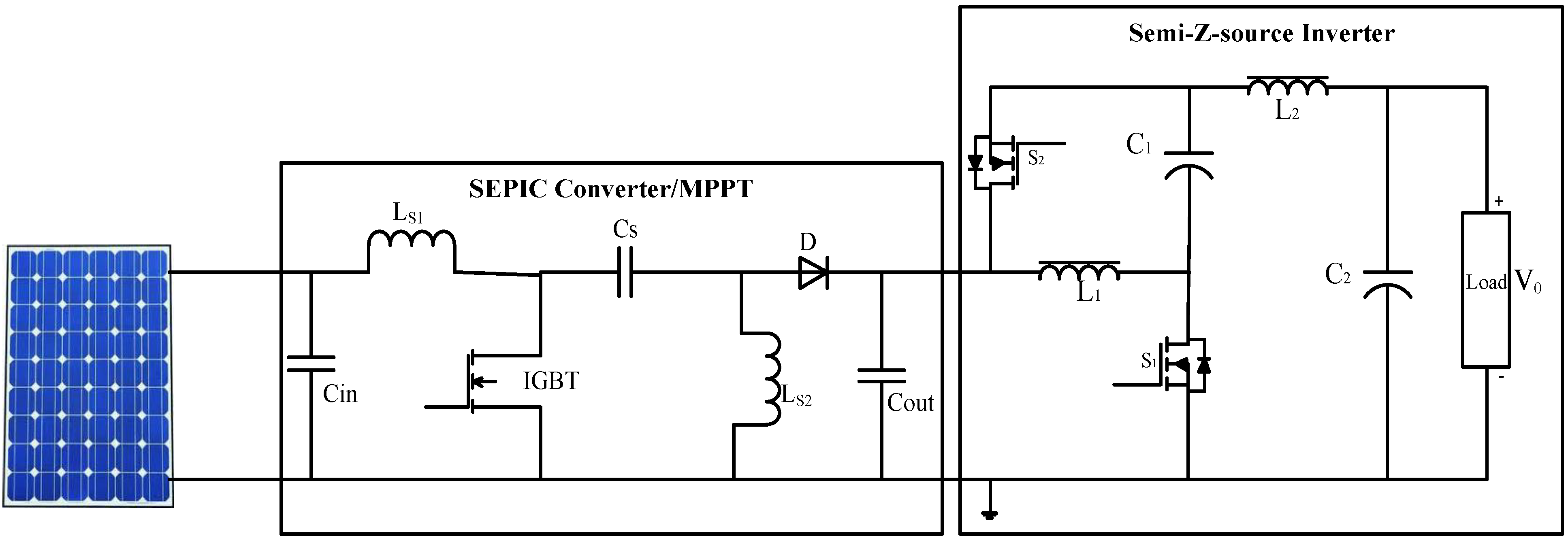
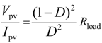
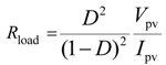
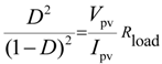
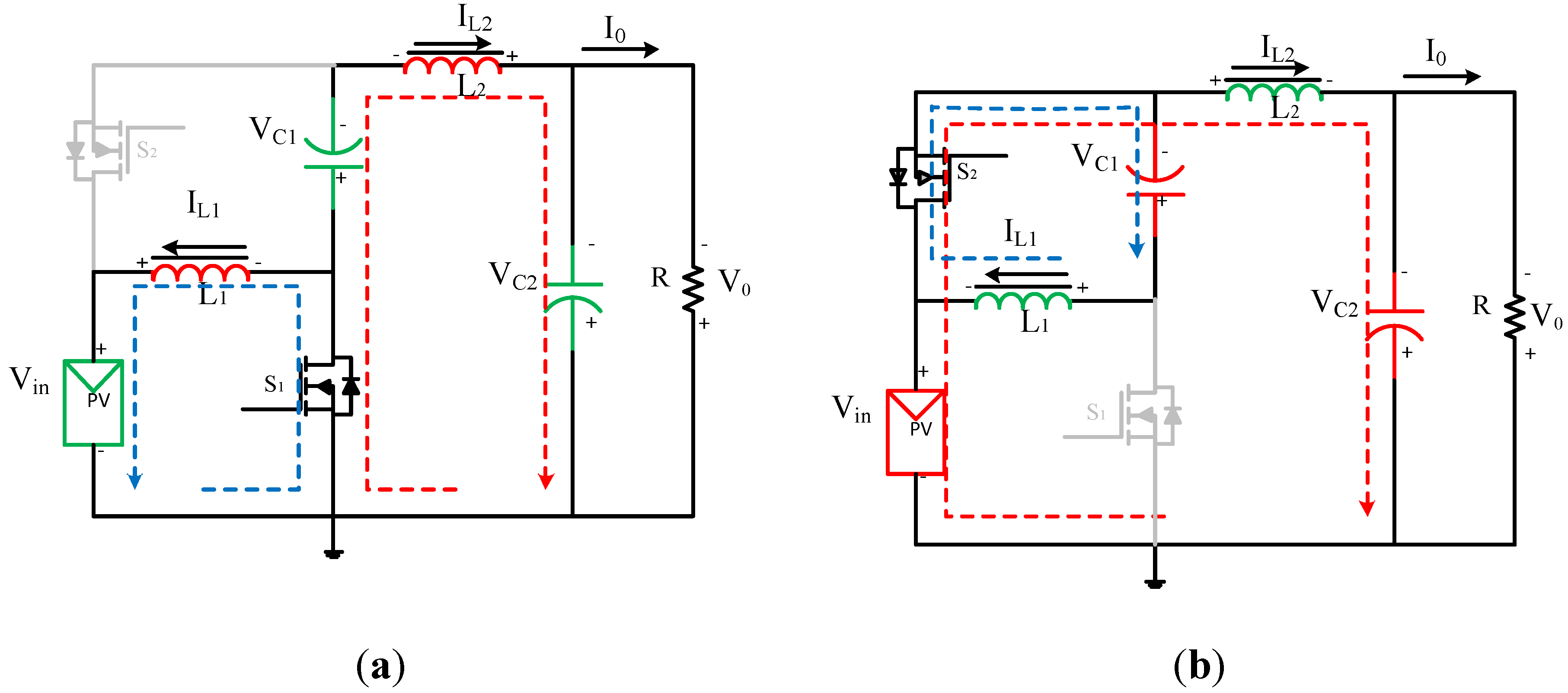
2.1.1. PV System with DC-DC Converter

A single ended primary inductor converter (SEPIC) has been used as a DC-DC converter for tracking the MPP of the PV array. The relationships between the voltage and current of the converter at the input and output sides are shown in Equations (1) and (2). The following equations are specifically required for SEPIC and may be different for other types of converter. Equation (3) shows that the duty cycle can be regulated, and thus, the input resistance (load line) of the converter can be varied until the load line cuts through the I-V curve at MPP:
Energies 07 03618 i001
Energies 07 03618 i002
Equation (1) is then divided by Equation (2) to obtain Equation (3) as follows:
Energies 07 03618 i003
where Vin is the input voltage of the converter or the voltage of the PV module Vpv; Iin is the input current of the converter or the current of the PV module Ipv; Rin is the input resistance of the converter or the resistance seen by the PV module; and Rout is the output resistance of the converter or load resistance Rload.

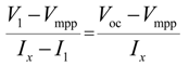
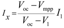
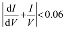
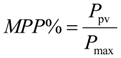
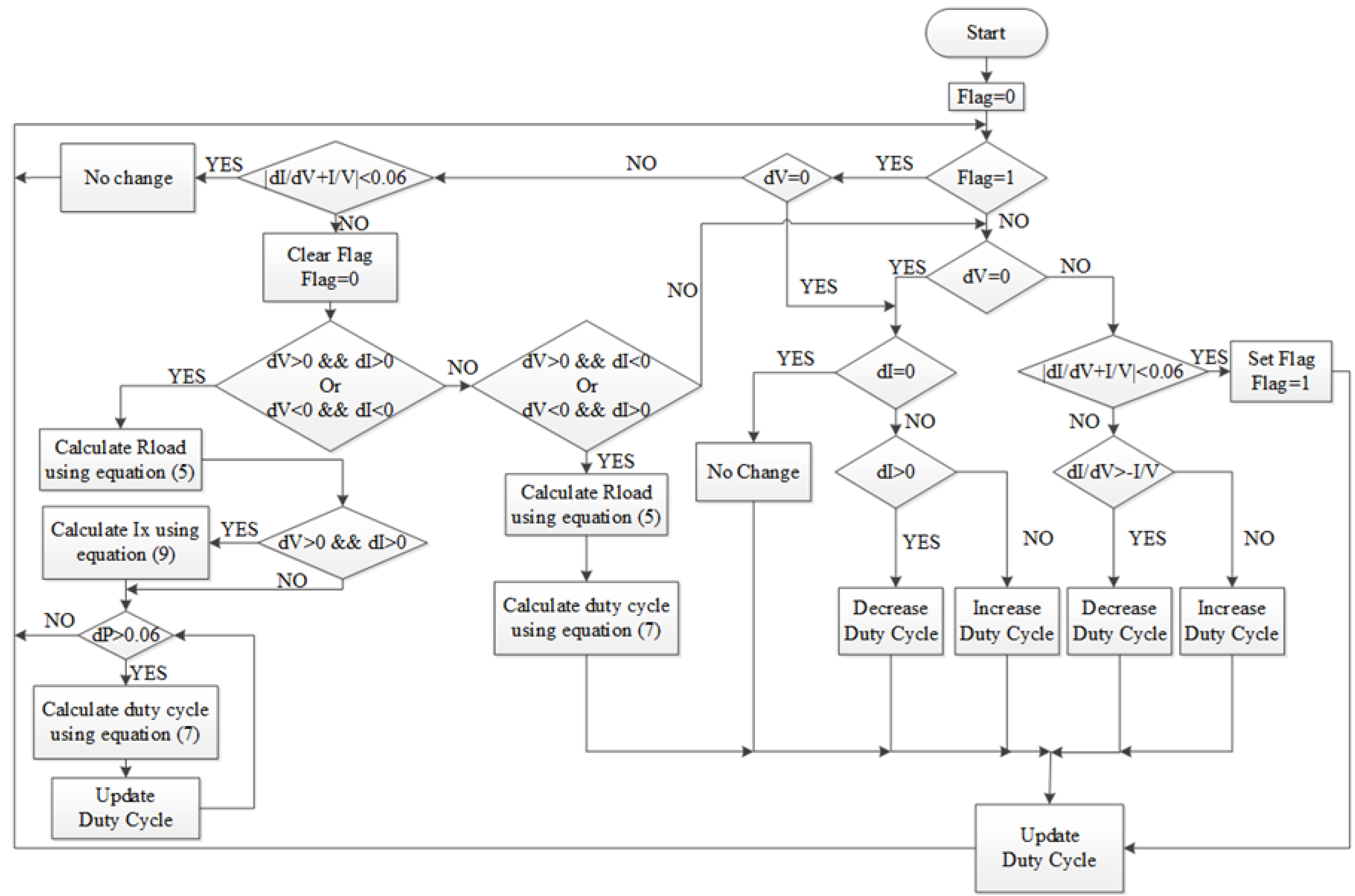
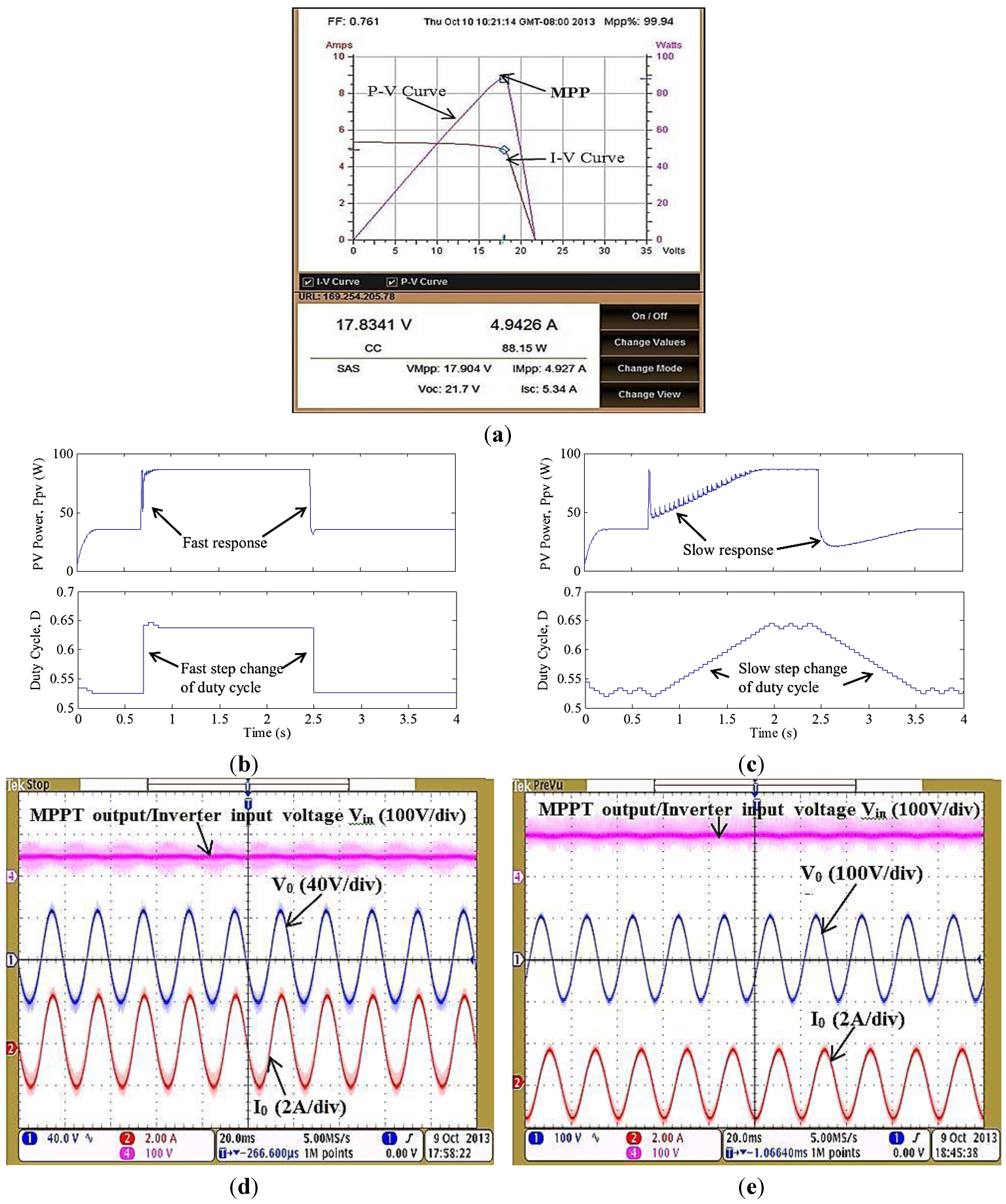
2.1.2. MPPT Algorithm

The proposed algorithm adopts the relationship between the load line and the I-V curve to introduce a fast-converging algorithm. In the proposed system, the voltage and current of the PV module are sensed by the MPPT controller. In the PV system, Equation (3) can be rewritten to obtain Equations (4) and (5) as follows:
Energies 07 03618 i004
Energies 07 03618 i005
The duty cycle, voltage, and current of the PV module are substituted into Equation (5) to obtain the load resistance. Then, the duty cycle can be calculated by substituting the desired voltage (Vmpp) and current (Impp) of the PV module into Equation (7) as follows:
Energies 07 03618 i006
Energies 07 03618 i007
where Energies 07 03618 i008.
In the proposed algorithm, the load of the PV system is calculated by using Equation (5). Then, Equation (7) is used to ensure that the system responds rapidly to operate near the new MPP after a increase or decrease in the solar irradiation. Meanwhile, for the variation in load, Equation (5) is used to calculate the new load resistance, and then Vmpp and Impp are substituted into Equation (7) to obtain the new duty cycle.

2.1.2.1. Decrease in Solar Irradiation Level

Initially, the PV system operates at load line 1 as in Figure 2a, the current and voltage of the PV module are represented by Vmpp and Impp. When the solar irradiation decreases, the operating point changes to load line 1, point A (V1, I1). The proposed algorithm is used to accelerate the convergence of the system. Therefore, the desired values of voltage and current are needed to substitute into Equation (7). Normally, the current of the PV module at the MPP is close to the short circuit current Isc (about 0.8Isc). When the solar irradiation decreases, the operating current of the PV module (I1) is near to the short circuit current Isc at 0.4 kW/m2, as shown in Figure 2a. Therefore, I1 can be approximated as Impp0.4. Generally, the MPP voltages for each level of solar irradiation are close to one another. Hence, the previous MPP voltage, Vmpp, and the operating current I1 are substituted into Equation (7) to obtain the new duty cycle. Then, the new duty cycle is applied to the converter, and the PV module operates at load line 3, point B (V2, I2), which is very close to the new MPP at 0.4 kW/m2 of solar irradiation. During only one sampling time, the operating point of the PV module is regulated from point A to B. Then, the conventional incremental conductance algorithm is applied to track the new MPP. With only a few more conventional steps, the proposed algorithm can track the new MPP at 0.4 kW/m2 which helps to reduce the convergence time from point A to point C.
Figure 2. Load lines on I-V curves for solar irradiation level of 0.4 kW/m2 and 1.0 kW/m2.
Energies 07 03618 g002

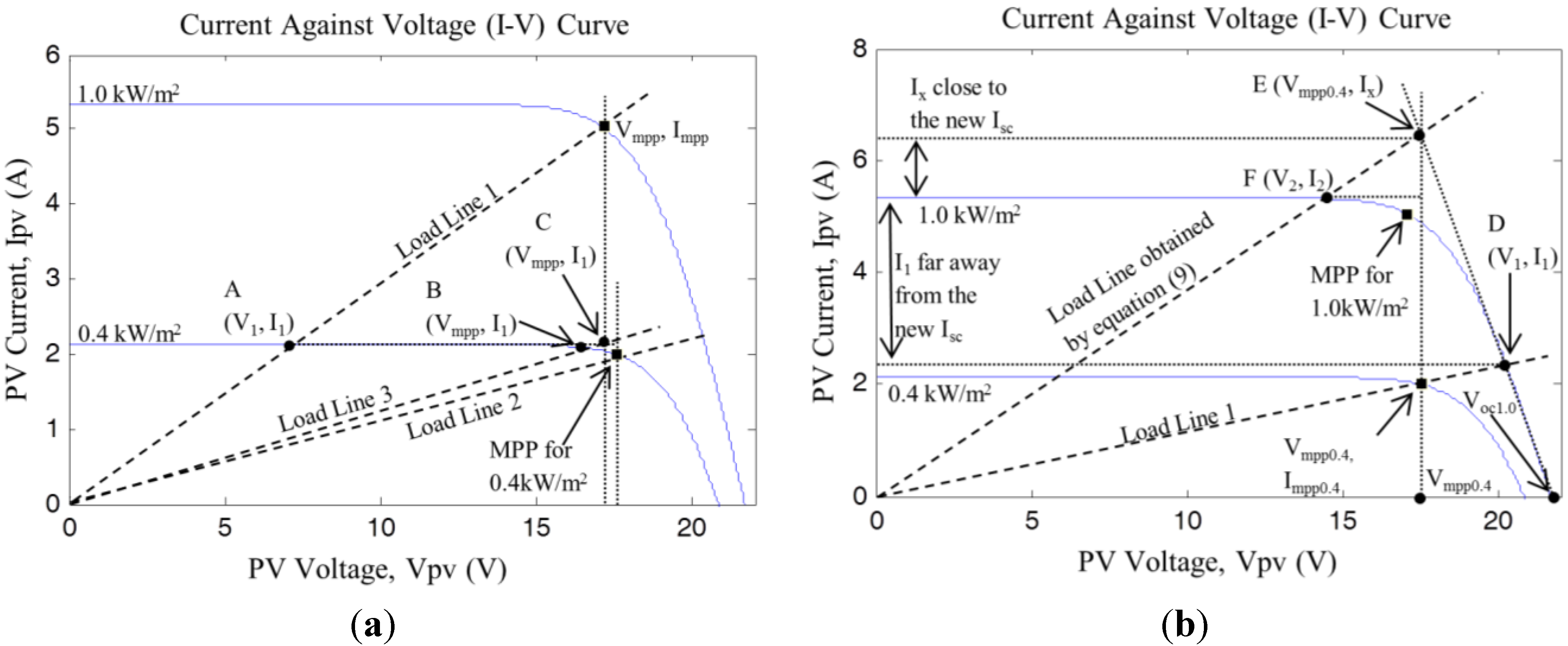
2.1.2.2. Increase in Solar Irradiation Level

Initially, the PV system operates at load line 1 as in Figure 2b, the current and voltage ratings of the PV module are Vmpp0.4 and Impp0.4, respectively. When the solar irradiation increases, the operating point changes to load line 1, point D (V1, I1). During the decrease in solar irradiation, the new operating current I1 is approximated as the new Impp. However, during the increase in solar irradiation, I1 cannot be approximated to Impp because it is far away from the short circuit current Isc for the new level of solar irradiation, as shown in Figure 2b. Therefore, an additional step is needed in this circumstance to ensure that the operating current of the PV module becomes close to the short circuit current. From Figure 2b, points E, Voc1.0, and Vmpp0.4 form a right-angled triangle. Then, trigonometic rule is used in Equation (8) to obtain the operating current Ix, which is near to the Isc for 1.0 kW/m2 of solar intensity. The open circuit voltage Voc of the PV module in Equation (9) is the estimated open circuit voltage obtained by Vmpp/0.8. Then, Vmpp is the voltage at the MPP before variation in solar irradiation. V1 is the voltage of PV module after the variation of solar irradiation:
Energies 07 03618 i009
Equation (8) is rearranged to obtain Equation (9):
Energies 07 03618 i010
In the second step, Ix and the voltage of the previous MPP i.e., Vmpp0.4 are substituted into Equation (7) to obtain the new duty cycle. With the new duty cycle, the PV module operates at point F (V2, I2), which is close to the new MPP at 1.0 kW/m2. Then, the conventional incremental conductance algorithm is used to track the MPP.

2.1.2.3. Load Variation

When the load is varied, the operating point of the PV module diverges from the MPP (change in load line position). A new duty cycle is required to ensure that the PV module operates at the MPP again. The new resistance of the load is calculated by using Equation (5). As variation only exists in the load and the I-V curve is unchanged, the voltage and current at the MPP remain unchanged. The Vmpp and Impp are substituted into Equation (7) to obtain the new duty cycle can be calculated after variation in the load. With the new duty cycle, the PV module operates at the point close to the MPP. The conventional algorithm is then used to track the MPP.
Figure 3 shows the flow chart of the proposed algorithm. A flag value is used to indicate that the PV system operates at the MPP if it is set to 1. Initially, the flag is clear. Then, the conventional incremental conductance algorithm is used to track the MPP. A permitted error of 0.06, shown in Equation (10), is used in the algorithm to eliminate steady-state oscillation in the system after the MPP is reached. The permitted error is chosen based on the duty cycle step size (0.005), and the accuracy in the power of the PV module at the MPP is ±0.7%:
Energies 07 03618 i011
Figure 3. Flow chart of the proposed MPPT algorithm.
Energies 07 03618 g003
When the MPP is tracked, the flag is set to 1. Then, Equation (10) is checked. If the equation is satisfied there is no variation in duty cycle. When there are variations in solar irradiation or load, Equation (10) no longer holds, and the flag is cleared. Then, Equation (5) is used to calculate the resistance of the load. If both the current and voltage of the PV module are decreased, Equation (7) is used to calculate the new duty cycle. If both the current and voltage of the PV module are increased, Ix is calculated by using Equation (9), and then, the new duty cycle is calculated using Equation (7). In the case of a nonlinear load, the response of the system is slower (not able to operate near the new MPP in single perturbation), and thus, changes in the power of the PV module are observed. If the power of the PV module increases, the algorithm will be in a loop; Equation (7) is used to calculate the new duty cycle. Until the difference in power (dP) is smaller than 0.06, then the algorithm goes into conventional algorithm. Meanwhile, for load variation, the new duty cycle is calculated using Equation (7) after the resistance of the load is obtained by Equation (5).

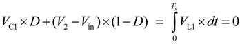
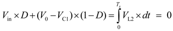
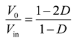
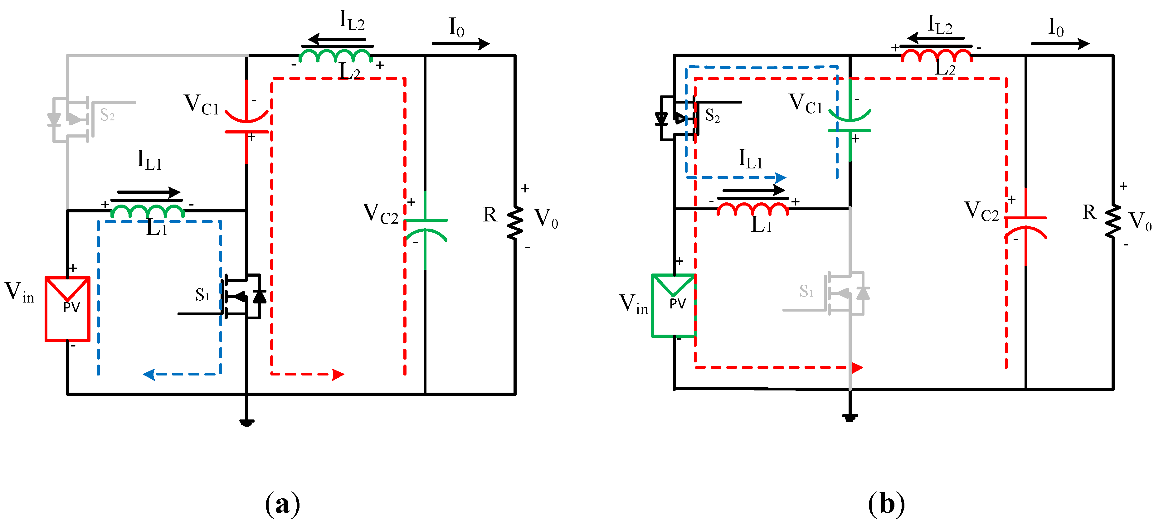
2.2. Semi-Z-Source Inverter Working Principle

Topology of the semi-Z-source inverter [46] as power conditioner is shown in Figure 4a and duty cycle vs. voltage gain curve is shown in Figure 4b. It is seen that when the duty cycle of the switch S1 varies from 0 to 1/2, the inverters can provide positive voltage at the output, whereas, from 1/2 to 2/3 the output voltage is negative. For the duty cycle of 1/2, the inverter produces zero voltage at output.
Figure 4. (a) Single phase doubly grounded semi-Z-source inverters, (b) voltage gain of Semi-Z-source inverters.
Energies 07 03618 g004
The single phase transformer-less semi-Z-source inverter topology shown in Figure 4a has been chosen to analyze steady state operation principle. Figure 5 and Figure 6 show the steady state operation of the semi-Z-source inverter. In state I, the switch S1 conducts while switch S2 does not conduct as shown in Figure 5a and Figure 6a. In state II, the switch S2 conducts while switch S1 does not conduct as shown in Figure 5b and Figure 6b. The duty cycle of Switch S1 is represented by D. Figure 5 represents the two states of operation respectively when the value of D < 0.5. In state I of Figure 5a, the switch S1 conducts to allow input voltage source and capacitor C1 charge the two inductors. In state II of Figure 5b, the switch S2 conducts and the two inductors have turned into sources. For both states, the output voltage has positive polarity. Figure 6 also represents the two states of operation for the value of D > 0.5. For this case, the current of the two inductors changes the direction with respect to Figure 5.
Figure 5. Modes of operation of semi-Z-source inverters when D < 0.5: (a) State I; (b) State II.
Energies 07 03618 g005
In state I of Figure 6a, the switch S1 conducts and the two inductors operate as two sources while in state II of Figure 6b, S2 conducts and input voltage source as well as capacitor C1 and C2 again charge the two inductors. For both states, output voltage has the negative polarity.
Figure 6. Modes of operation of semi-Z-source inverters when D > 0.5: (a) State I; (b) State II.
Energies 07 03618 g006
For the following steady state equations the capacitors C1 and C2 voltages have been considered as VC1 and VC2 respectively. Also, the directions of current references of the inductor and the voltage references of the capacitor are shown in the Figure 5 and Figure 6 have been considered for the following steady state equations. The steady state equations can be derived based on inductor voltage-second balance and capacitor charge balance principle. Applying net volt-seconds balance principle to inductor L1 over one switching period, it can be found that:
Energies 07 03618 i012
Applying net volt-seconds balance principle to inductor L2 over one switching period, it can be found:
Energies 07 03618 i013
From Equations (11) and (12), it can be said that:
VC1 = Vin
Energies 07 03618 i014
By applying net capacitor charge balance principle to capacitor C1 and C2 over one switching period, the following equations can be derived:
Energies 07 03618 i015
IL2 = − I0
Energies 07 03618 i016
If it can be assumed that, inverter output voltage is Equation (18) then the modulation index can be expressed as in Equation (19):
V0 = V sin ωt
Energies 07 03618 i017
By substituting the values from Equations (18) and (19) into Equation (14), it can be found:
Energies 07 03618 i018
The duty cycle of the switch S2 is D′ = 1-D, which can be expressed as Equation (21):
Energies 07 03618 i019
Let the output current expressed in Equation (22) have the same phase as the output voltage. Voltage across the switch during the OFF state can be presented by Equation (23), which is depicted in Figure 7a. Current through the switch during the ON state can be expressed by Equation (24) which is shown in Figure 7b. It can be inferred from Figure 7a along with Equation (23) that, the maximum OFF state voltage across the switch is 3Vin. At the same time, the maximum ON state current through the switch can be determined from Figure 7b along with Equation (24) and the value is 3I. For both these cases, the value of D = 2/3, the value of M = 1 and the value of ωt = 3π/2:
Io = I sin ωt
Energies 07 03618 i020
Energies 07 03618 i021
Figure 7. (a) Off state voltage across the switch vs. M and ωt, (b) On state current through the switch vs. M and ωt.
Energies 07 03618 g007
Voltage across capacitor C1 can be derived from Equations (15) and (20) which is shown in Equation (25). Figure 8a shows the graphical representation of Equation (25). As depicted in this figure, the maximum voltage across capacitor C1 is 2Vin when, the value of D = 2/3, the value of M = 1 and the value of ωt = 3π/2.
Figure 8. (a) Voltage across capacitor C1 vs. M and ωt; (b) Current through inductor L1 vs. M and ωt.
Energies 07 03618 g008
In the same way, current through inductor L1 is stated in Equation (26) which derived from Equations (17), (20) and (22). Current through inductor L1 is shown in Figure 8b and the maximum current through inductor L1 is 2I when, the value of D = 2/3, the value of M = 1 and the value of ωt = 3π/2:
Energies 07 03618 i022
Energies 07 03618 i023
Voltage ripple of the capacitor C1 and the current ripple of the inductor can be dictated by Equations (27) and (28) respectively considering L1 = L2. Voltage ripple of the capacitor C1 is presented in Figure 9a with respect to the modulation index M and output phase angle ωt. By using Equations (25), (27) and Figure 8a, the value of capacitance C1 can be calculated by considering the peak ripple requirement of the current. Current ripple of the inductor L1 is depicted in Figure 9b with respect to modulation index M and output phase angle ωt. Now, from Equations (26), (28) and Figure 8b, the value of inductance L1 can be selected by considering the peak ripple requirement of the current. More details can be found in [41]:
Energies 07 03618 i024
Energies 07 03618 i025
Figure 9. (a) Voltage ripple capacitor C1; (b) Current ripple of inductor L1.
Energies 07 03618 g009

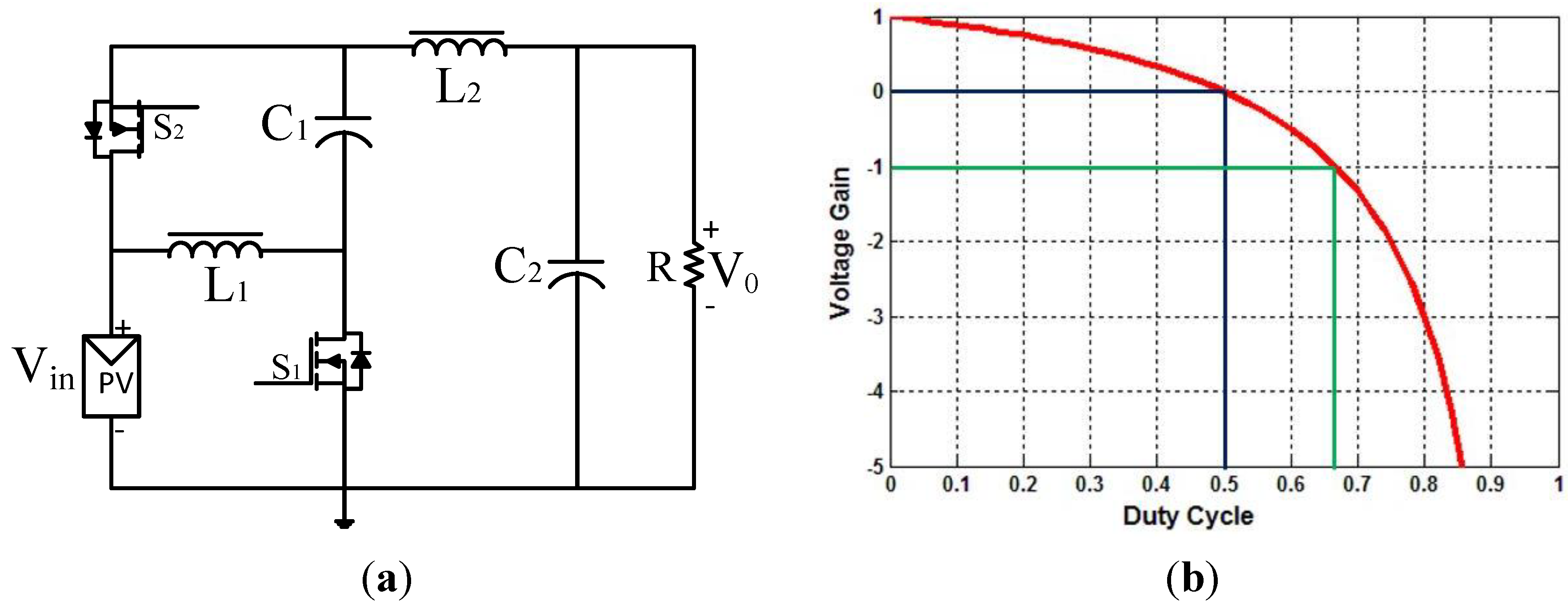
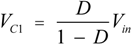
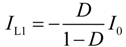
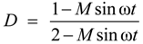
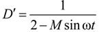
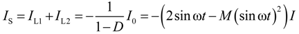
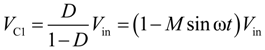
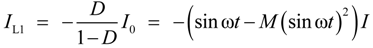
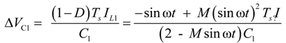
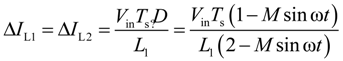
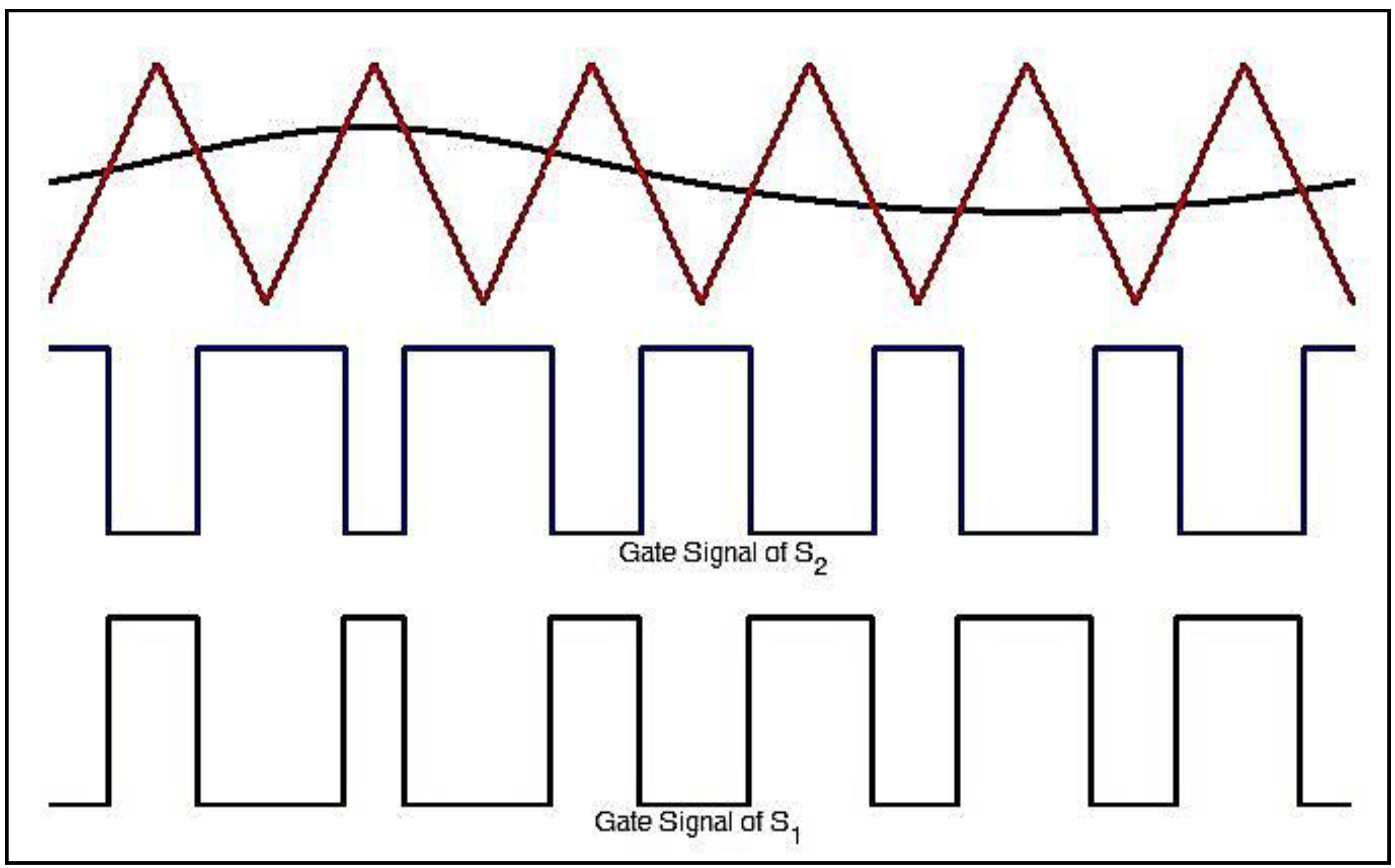
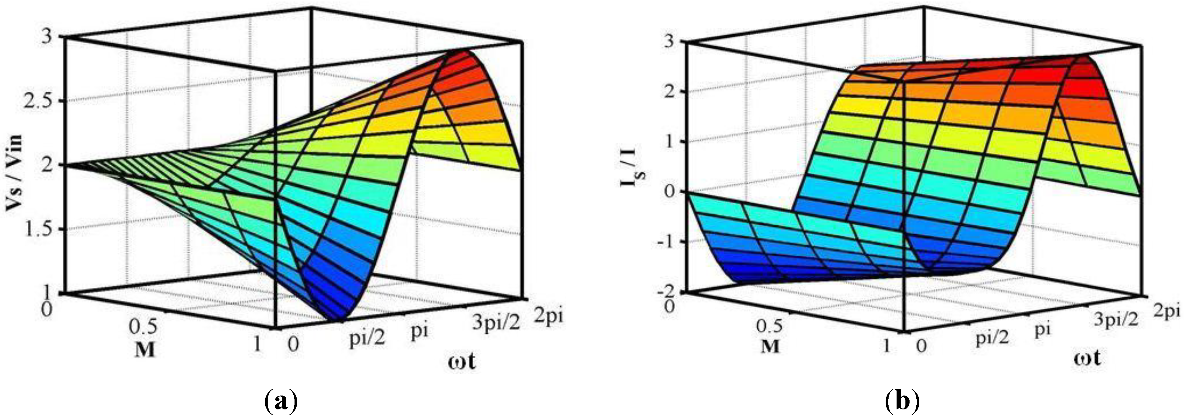
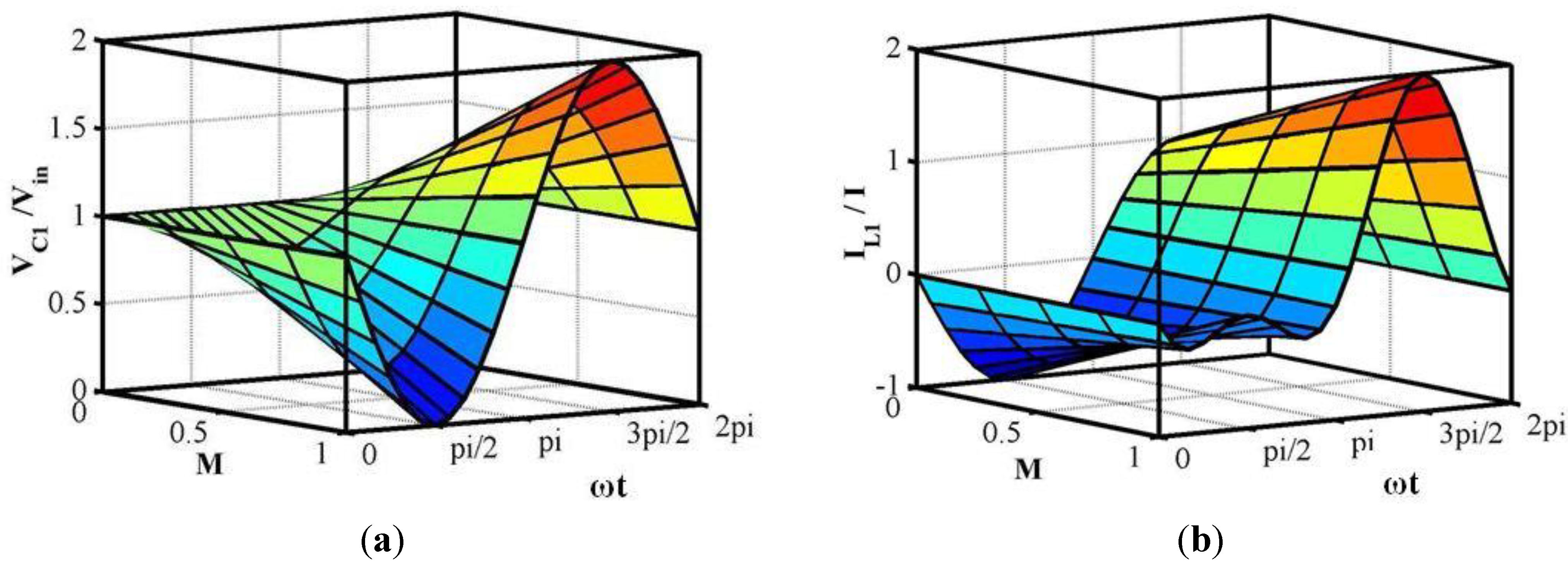
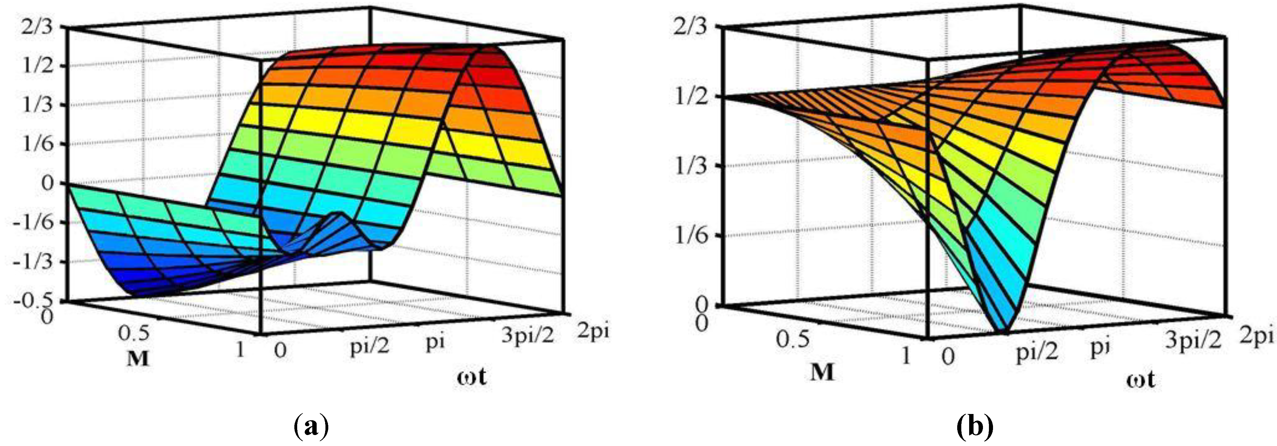
2.3. Semi-Z-Source Inverter Modulation Principle

It is possible to control the voltage gain polarity by controlling the duty cycle of the switch, but the relation between duty cycle and voltage gain is a straight line for a traditional full bridge inverter and for this reason, to generate a sinusoidal voltage at the output, the SPWM technique is used [46]. On the contrary, the semi-Z-source inverter has a nonlinear relation between voltage gain, so a nonlinear SPWM is used to generate a sinusoidal wave, as shown in Figure 10. A derived reference voltage is shown in Equation (21) to control the duty cycle of switch S2. To turn on switch S2, it is necessary that the reference value should be greater than carrier value. Equation (20) shows the reference signal for controlling the duty cycle of switch S1 which is complementary from the duty cycle of switch S2 and the range of modulation index is between 0 and 1. Figure 10 shows the switching signals of the two switches S1 and S2 at the time when the modulation index is 2/3.
Figure 10. Modulation principle of semi-Z-source inverter.
Energies 07 03618 g010

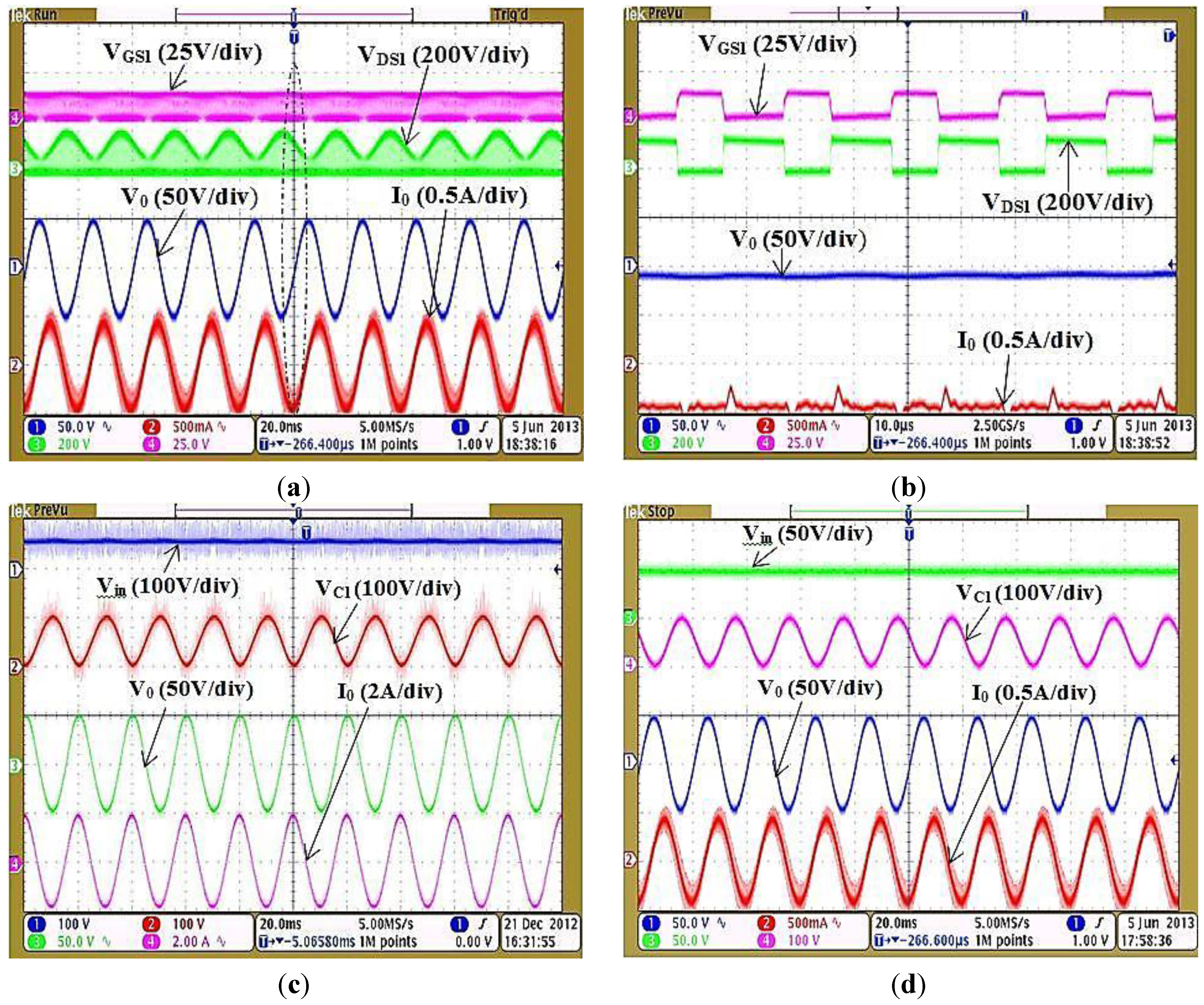
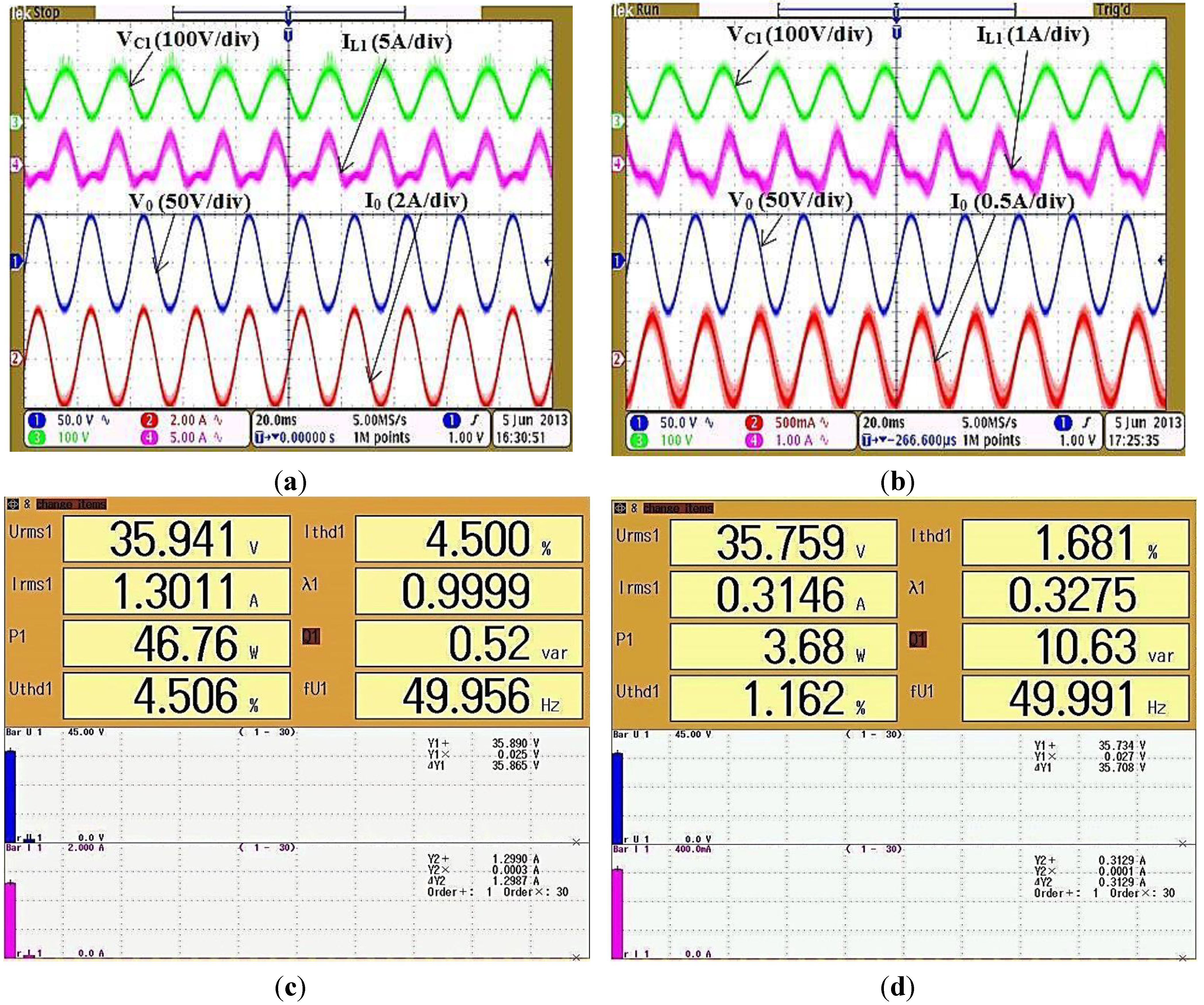
2.4. Experimental Validation of Semi-Z-Source Inverter

For the purpose of experimental validation, a prototype rated 48-W, 50 Hz transformer-less semi-Z-source inverter is constructed according to the diagram shown in Figure 4a. The input voltage of this prototype is around 50 V and output voltage is around 35.35 V. The switching frequency of this system is 50 kHz. It is seen from Figure 7a that the maximum off state voltage that is needed to withstand by the switch is 150 V. Here, for the prototype, two MOSFETs (STP75NF20) are chosen as switches. According to the design procedure mentioned earlier, the peak voltage across the capacitor C1 is 100 V. The values of both the capacitor C1 and C2 are 4.7 µF considering voltage ripple is limited to 5.75% of the peak voltage across the capacitors. For the prototype, polyester film capacitors (MPE475K) are chosen. A performance real time target machine (SPEEDGOAT) has been used to produce the switching signals for the inverter.
Two inductors (L1 and L2) used in semi-Z-source inverters can be placed in a single core or in two different cores. To minimize the input current ripple and to reduce the size, the coupled inductor method is chosen for the prototype thus ensuring identical current flow. For high frequency operation, ferrite materials have low loss features and for this, a magnetic core of ferrite material (45528EE) is chosen for this prototype. To prevent the inductor core from saturation under load, an air gap is used within the core structure because the energy being stored in air gap will prevent the core from saturation under load. For the prototype, the maximum load current peak value is around 2A. According to the design procedure mentioned earlier, the peak current of inductor L1 is 4A. The value of the inductor L1 is 400 µH considering the current ripple is limited to 1/3 of the peak current of the inductor. The values of the inductor L2 is also 400 µH that can be calculated by the same procedure. Finally, the total harmonic distortion (THD) of the output voltage and current has been analyzed using a YOKOGAWA WT 1800 precision power analyzer.
Experimental results of the laboratory prototype model of 48-W transformer-less semi-Z-source inverter are shown in Figure 11, Figure 12 and Figure 13. The prototype has been tested under R load and R-L load. During the laboratory experiments, around 50 V input voltage has been applied and modulation index has been fixed to 0.95. Around 27 Ω resistance and 285 mH inductance have been used as load.
Figure 11. (a) Experimental waveforms of gate to source voltage, drain to source voltage, output voltage, output current for R load; (b) zoomed in waveform of (a); (c) experimental waveforms of drain to source voltage of two switches, output voltage, output current for R load; (d) zoomed in waveform of figure (c).
Energies 07 03618 g011
Figure 11a,b shows the gate to source voltage VGS1 of switch S1, drain to source voltage VDS1 of switch S1, output voltage V0, output current I0 and their zoomed version respectively during R load condition. VGS1 and VDS1 of switch S1 are operating in completely reverse according to the given figures. In addition, output voltage polarity changes with the change of duty cycle of the switch which satisfies the theoretical background. Drain to source voltage VDS1 of switch S1, drain to source voltage VDS2 of switch S2, output voltage V0, output current I0 and certain magnified versions of the are represented in Figure 11c,d respectively. It can be said that like the theoretical background suggests, these two switches are operating in a complementary manner with 50 kHz switching frequency and maximum off state voltage across the switches are three times of input voltage. Figure 12a,b illustrate the experimental results of gate to source voltage VGS1 of switch S1, drain to source voltage VDS1 of switch S1, output voltage V0, output current I0 and their zoomed version respectively during R-L load condition.
Figure 12. (a) Experimental waveforms of gate to source voltage, drain to source voltage, output voltage, output current for R-L load; (b) zoomed in waveform of figure (a); (c) experimental waveforms of input DC voltage, capacitor C1 voltage, output voltage, output current for R load; (d) experimental waveforms of input DC voltage, capacitor C1 voltage, output voltage, output current for R-L load.
Energies 07 03618 g012
When R-L is considered as load, except for output current and voltage, the remaining results are almost same as R load. It is observed that the output current is lagging the output voltage and the magnitude of the output current decreases as the load increases. Waveforms of input voltage Vin, voltage across capacitor C1, output voltage V0 and output current I0 for R and R-L load are shown in Figure 12c,d respectively. These two figures illustrate that the peak capacitor voltage is twice the input voltage for both the R and R-L load. Moreover, both the positive and negative peak values of the output voltage are equal to input voltage. Furthermore, during experiment, the input voltage has been measured between DC+ terminal and ground for both the R and R-L load. Figure 12c,d show that for both the R and R-L load condition, the input voltage Vin is almost constant and contains no high frequency variation. As a consequence, the generation of common mode voltage is minimized which in turns results in reduction of common mode leakage current.
Figure 13. (a) Experimental waveforms of input DC voltage, capacitor C1 voltage, output voltage, output current for R load; (b) experimental waveforms of input DC voltage, capacitor C1 voltage, output voltage, output current for R-L load; (c) THD and Harmonic spectrum of output voltage and current for R load; (d) THD and Harmonic spectrum of output voltage and current for R-L load.
Energies 07 03618 g013
The voltage across capacitor C1, current through inductor L1, output voltage and output current of the inverter for both R and R-L loads are shown in Figure 13a,b respectively. Both the figures indicate the voltage developed across the capacitor C1 followed by the inductor current IL1 and inductor current is approximately twice the output current for both the load conditions.
THD and harmonic spectrum of the output voltage and current for R, and R-L load are displayed in Figure 13c,d respectively. It can be seen from these figures that, for R load the inverter produce RMS output voltage of 35.94 V with THD of 4.506% and RMS output current of 1.30 A with THD of 4.50%. While for R-L load the inverter produces RMS output voltage of 35.76 V with THD of 1.16% and RMS output current of 0.315 A with THD of 1.68%. In case of R load the inverter supplies real power of 46.76 W at unity power factor. On the other hand, the inverter supplies real power of 3.68 W and reactive power of 10.62 var for R-L load. In addition, for both the R and R-L load condition, THD’s are within the limit (less than 5%), no occurrence of DC current component and percentage of higher order harmonic components are very negligible at the output because coupled inductors have the ability to reduce the input current ripple and output voltage ripple which satisfies the limits mentioned in [33,36].

3. Experimental Validation of Single Phase Semi-Z-Source Inverter for PV System with MPPT

For the purposes of experimental validation of the complete single phase semi-Z-source inverter with MPPT system, a practical experimental MPPT setup connected with a semi-Z-source inverter has been applied to the PV module according to Figure 1. To consider the practical behavior of the PV module, a solar Array Simulator from Agilent Technologies (E4360A) has been used in the laboratory. The complete experimental setup of the prototype has been tested for two different DC output MPPT voltage levels with two different types of load of R and R-L. For the complete experimental setup, a 20 Ω resistor and 285 mH inductor have been used as load.
Figure 14a represents the waveforms of the I-V curve and P-V curve during experimental condition. It is depicted from this figure that, PV is working at MPP with tracking efficiency of 99.94%. The MPP tracking efficiency has been calculated by taking the ratio between averaged output power obtained under steady state and maximum available power of the PV array [11]. As the solar Array Simulator from Agilent Technologies (E4360A) has been used here, the maximum available power, Pmax is the maximum power point of the PV module. When the simulator is connected to the load, the power supplied or the power of the PV module, Ppv has been measured and compare to the maximum power available from the PV module. Thus, the MPP efficiency is calculated by the simulator by using the Equation (29):
Energies 07 03618 i026
Figure 14b,c depict simulation results of PV module power and duty cycle of the proposed fast-converging algorithm and conventional incremental conductance algorithm respectively for experimental condition. It is seen that the proposed algorithm response is faster and contains much less steady state oscillation than the conventional incremental conductance algorithm under fast varying solar intensity conditions. At t = 0.65 s, the solar irradiation is increased from 0.4 kW/m2 to 1.0 kW/m2 and at t = 2.48 s, the solar irradiation is decreased back to 0.4 kW/m2. The response of the conventional algorithm is slow due to the constant step change in the duty cycle.
Figure 14. (a) Waveform of PV module power and duty cycle of proposed algorithm; (b) waveform of PV module power and duty cycle of conventional incremental conductance algorithm; (c) I–V curve and P–V curve; (d) experimental waveforms of MPPT output/inverter input DC voltage, output voltage, output current for R load; (e) experimental waveforms of MPPT output/inverter input DC voltage, output voltage, output current for R-L load.
Energies 07 03618 g014
A comparison of the proposed algorithm with the conventional incremental conductance and modified incremental conductance is shown in Table 1. It can be concluded that there is no steady state oscillation in the proposed algorithm as compared to the conventional incremental conductance algorithm. Other than that, the response time of the proposed algorithm is also faster than the conventional incremental conductance algorithm during fast varying solar irradiation. Finally, the efficiency of the proposed algorithm (99.94%) is the highest compared with the efficiency of the conventional and modified incremental conductance algorithm shown in [20].
Table 1. Comparison of the proposed algorithm with the conventional incremental conductance and modified incremental conductance algorithm.
ParametersConventional Incremental Conductance algorithm [20]Modified incremental conductance algorithm [20]Proposed fast convergence algorithm
Steady state oscillationYesNoNo
Response under fast varying solar irradiationSlowFastFast
MPP efficiency (%)98.4999.8999.94
Figure 14d shows the experimental results of R load where the output voltage of DC/DC converter of MPPT acts as the input DC voltage of around 45 V of the inverter. This figure represents that the inverter produces a sinusoidal output voltage with 90 V peak-peak and sinusoidal current of around 4.5 A as 20 Ω resistance has been applied as load. In addition, there is no phase difference between the output voltage and the current of the inverter. Moreover, during the experiment the input voltage of the inverter has been measured between the DC+ terminal and ground. Figure 14d displays that the input voltage Vin is almost constant and contains no high frequency variation. As a consequence, the generation of common mode voltage is minimized which in turns reduces the common mode leakage current. The experimental waveforms of R-L load when the output voltage of DC/DC converter of MPPT has been fixed to the DC voltage of around 100 V which acts as the input voltage of inverter is shown in Figure 14e. It is observed from this figure that, the inverter produces sinusoidal output voltage with 200 V peak-peak and sinusoidal current of around 3.2 A as 20 Ω resistance and 285 mH inductance have been applied as load. In addition, there is phase difference between output voltage and current of the inverter. Figure 14d displays that, the input voltage Vin is almost constant and contains no high frequency variation. As a consequence, the generation of common mode voltage is minimized for R-L load conditions, which in turns reduces of common mode leakage current, so it can be said that the proposed MPPT based semi-Z-source inverter is acceptable for PV systems for tracking the maximum power of the PV array and to generate adjustable sinusoidal output voltage with the minimization of common mode leakage current by doubly grounded features.

4. Conclusions

This paper presents a doubly grounded semi-Z-source inverter with a MPPT controller for PV systems. This low cost, downsized micro-modular system is applicable for connecting utility grids with standalone PV power conditioners and interfacing PV systems because this system is able to track the MPP of PV arrays and produce an AC voltage at their output by utilizing only three switches. The experimental results demonstrate that by utilizing fast-converging algorithm this inverter system is capable to track the maximum power from the PV array which is fast in response. Also, this system is able to minimize common mode leakage currents for PV arrays by its doubly grounded features. Other than that, it can convert the DC power of a PV array to AC power with reduced THD and DC current at the output by utilizing the coupled inductor technique. Moreover, the tracking efficiency of the MPP is 99.94%, which is higher than that of conventional and modified incremental conductance algorithms.

Acknowledgments

The authors would like to thank the Ministry of Higher Education of Malaysia and University of Malaya for providing financial support under the UMRG project RP015A-13AET.

Author Contributions

In this paper, Tofael Ahmed contributes to the design and implementation of semi-Z-source inverter and writing the manuscript. Tey Kok Soon contributes to the design, implementation and writting of the section MPPT. Saad Mekhilef provides overall supervision and guidance to finalyze the work. All the authors read and approve the manuscript.

Conflicts of Interest

The authors declare no conflict of interest.

References

  1. Desai, H.P.; Patel, H. Maximum power point algorithm in PV generation: An overview. In Proceedings of the 2007 7th International Conference on Power Electronics and Drive Systems, Bangkok, Thailand, 27–30 November 2007; pp. 624–630.
  2. Xiao, L.; Yaoyu, L.; Seem, J.E. Maximum power point tracking for photovoltaic system using adaptive extremum seeking control. IEEE Trans. Control Syst. Technol. 2013, 21, 2315–2322. [Google Scholar] [CrossRef]
  3. Shen, J.-M.; Jou, H.-L.; Wu, J.-C. Novel transformerless grid-connected power converter with negative grounding for photovoltaic generation system. IEEE Trans. Power Electron. 2012, 27, 1818–1829. [Google Scholar] [CrossRef]
  4. Kasem Alaboudy, A.H.; Zeineldin, H.H.; Kirtley, J.L. Microgrid stability characterization subsequent to fault-triggered islanding incidents. IEEE Trans Power Deliv. 2012, 27, 658–669. [Google Scholar] [CrossRef]
  5. Meneses, D.; Blaabjerg, F.; Garcia, O.; Cobos, J.A. Review and comparison of step-up transformerless topologies for photovoltaic AC-module application. IEEE Trans. Power Electron. 2013, 28, 2649–2663. [Google Scholar] [CrossRef]
  6. Ahmed, M.E.-S.; Orabi, M.; AbdelRahim, O.M. Two-stage micro-grid inverter with high-voltage gain for photovoltaic applications. IET Power Electron. 2013, 6, 1812–1821. [Google Scholar] [CrossRef]
  7. Elgendy, M.A.; Zahawi, B.; Atkinson, D.J. Assessment of perturb and observe MPPT algorithm implementation techniques for PV pumping applications. IEEE Trans. Sustain. Energy 2012, 3, 21–33. [Google Scholar] [CrossRef]
  8. Sera, D.; Mathe, L.; Kerekes, T.; Spataru, S.V.; Teodorescu, R. On the perturb-and-observe and incremental conductance MPPT methods for PV systems. IEEE J. Photovolt. 2013, 3, 1070–1078. [Google Scholar] [CrossRef]
  9. Safari, A.; Mekhilef, S. Simulation and hardware implementation of incremental conductance mppt with direct control method using CUK converter. IEEE Trans. Ind. Electron. 2011, 58, 1154–1161. [Google Scholar]
  10. Ishaque, K.; Salam, Z.; Amjad, M.; Mekhilef, S. An improved particle swarm optimization (PSO)-based MPPT for PV with reduced steady-state oscillation. IEEE Trans. Power Electron. 2012, 27, 3627–3638. [Google Scholar] [CrossRef]
  11. Liu, Y.-H.; Huang, S.-C.; Huang, J.-W.; Liang, W.-C. A particle swarm optimization-based maximum power point tracking algorithm for PV systems operating under partially shaded conditions. IEEE Trans. Energy Convers. 2012, 27, 1027–1035. [Google Scholar] [CrossRef]
  12. El Khateb, A.; Rahim, N.A.; Selvaraj, J.; Uddin, M.N. Fuzzy logic controller based SEPIC converter for maximum power point tracking. IEEE Trans. Ind. Appl. 2014, PP, 1. [Google Scholar]
  13. Alajmi, B.N.; Ahmed, K.H.; Finney, S.J.; Williams, B.W. Fuzzy-logic-control approach of a modified hill-climbing method for maximum power point in microgrid standalone photovoltaic system. IEEE Trans. Power Electron. 2011, 26, 1022–1030. [Google Scholar] [CrossRef]
  14. Lin, W.-M.; Hong, C.-M.; Chen, C.-H. Neural-network-based MPPT control of a stand-alone hybrid power generation system. IEEE Trans. Power Electron. 2011, 26, 3571–3581. [Google Scholar] [CrossRef]
  15. Zhang, F.; Thanapalan, K.; Maddy, J.; Guwy, A. Development of a novel hybrid maximum power point tracking methodology for photovoltaic systems. In Proceedings of the 18th IEEE International Conference on Automation and Computing, Loughborough, UK, 7–8 September 2012; pp. 1–6.
  16. Al-Diab, A.; Sourkounis, C. Variable step size P&O MPPT algorithm for PV systems. In Proceedings of the 12th International Conference on Optimization of Electrical and Electronic Equipment, Brasov, Romania, 20–22 May 2010; 2010; pp. 1097–1102. [Google Scholar]
  17. Chao, K.-H.; Li, C.-J. An intelligent maximum power point tracking method based on extension theory for PV systems. Expert Syst. Appl. 2010, 37, 1050–1055. [Google Scholar] [CrossRef]
  18. Liu, F.; Duan, S.; Liu, F.; Liu, B.; Kang, Y. A variable step size INC MPPT method for PV systems. IEEE Trans. Ind. Electron. 2008, 55, 2622–2628. [Google Scholar] [CrossRef]
  19. Zbeeb, A.; Devabhaktuni, V.; Sebak, A. Improved photovoltaic MPPT algorithm adapted for unstable atmospheric conditions and partial shading. In Proceedings of the 2009 International Conference on Clean Electrical Power, Capri, Italy, 9–11 June 2009; pp. 320–323.
  20. Tey, K.S.; Mekhilef, S. Modified incremental conductance MPPT algorithm to mitigate inaccurate responses under fast-changing solar irradiation level. Solar Energy 2014, 101, 333–342. [Google Scholar] [CrossRef]
  21. Kerekes, T.; Teodorescu, R.; Liserre, M.; Klumpner, C.; Sumner, M. Evaluation of three-phase transformerless photovoltaic inverter topologies. IEEE Trans. Power Electron. 2009, 24, 2202–2211. [Google Scholar] [CrossRef]
  22. Haeberlin, H.; Borgna, L.; Kaempfer, M.; Zwahlen, U. New Tests at Grid-Connected PV Inverters: Overview over Test Results and Measured Values of Total Efficiency ηtot. In Proceedings of the 21st European Photovoltaic Solar Energy Conference, Dresden, Germany, 4–8 September 2006.
  23. Martínez-Moreno, F.; Lorenzo, E.; Muñoz, J.; Moretón, R. On the testing of large PV arrays. Prog. Photovolt.: Res. Appl. 2012, 20, 100–105. [Google Scholar] [CrossRef] [Green Version]
  24. Araújo, S.V.; Zacharias, P.; Mallwitz, R. Highly efficient single-phase transformerless inverters for grid-connected photovoltaic systems. IEEE Trans. Ind. Electron. 2010, 57, 3118–3128. [Google Scholar] [CrossRef]
  25. Eltawil, M.A.; Zhao, Z. Grid-connected photovoltaic power systems: Technical and potential problems—A review. Renew. Sustain. Energy Rev. 2010, 14, 112–129. [Google Scholar] [CrossRef]
  26. Lopez, O.; Freijedo, F.D.; Yepes, A.G.; Fernandez-Comesana, P.; Malvar, J.; Teodorescu, R.; Doval-Gandoy, J. Eliminating ground current in a transformerless photovoltaic application. IEEE Trans. Energy Convers. 2010, 25, 140–147. [Google Scholar]
  27. Xiao, H.F.; Xie, S.J. Leakage current analytical model and application in single-phase transformerless photovoltaic grid-connected inverter. IEEE Trans. Electromagn. Compat. 2010, 52, 902–913. [Google Scholar] [CrossRef]
  28. Yang, B.; Li, W.H.; Gu, Y.J.; Cui, W.F.; He, X.N. Improved transformerless inverter with common-mode leakage current elimination for a photovoltaic grid-connected power system. IEEE Trans. Power Electron. 2012, 27, 752–762. [Google Scholar]
  29. Zhang, F.; Yang, S.; Peng, F.Z.; Qian, Z. A zigzag cascaded multilevel inverter topology with self voltage balancing. In Proceedings of the Twenty-Third Annual IEEE Applied Power Electronics Conference and Exposition 2008, Austin, TX, USA, 24–28 February 2008; pp. 1632–1635.
  30. Ahmed, T.; Mekhilef, S.; Nakaoka, M. Single phase transformerless semi-Z-source inverter with reduced total harmonic distortion (THD) and DC current injection. In 5th Annual International Energy Conversion Congress and Exibition for the Asia Pacific Region (IEEE ECCE Asia DownUnder), Melbourne, Australia, 3–6 June, 2013; pp. 1322–1327.
  31. Blewitt, W.M.; Atkinson, D.J.; Kelly, J.; Lakin, R.A. Approach to low-cost prevention of DC injection in transformerless grid connected inverters. IET Power Electron. 2010, 3, 111–119. [Google Scholar] [CrossRef]
  32. Calais, M.; Ruscoe, A.; Dymond, M. Transformerless PV inverter issues revisited–are australian standards adequate? In Proceedings of 2009 the 47th Annual Conference ANZSES Annual Conference, Townsville, Australia, 29 September–2 October 2009.
  33. IEEE. IEEE Standard for Interconnecting Distributed Resourceswith Electric Power Systems; IEEE Standard 1547–2003; IEEE: New York, NY, USA, 2003; pp. 1–16. [Google Scholar]
  34. British Standards Institution. Characteristics of the Utility Interface for Photovoltaic (PV) SystemsIEC 61727, 2nd ed.; British Standards Institution: London, UK, 2004. [Google Scholar]
  35. IEEE. Recommended Practice for Utility Interface of Photovoltaic (PV) Systems; IEEE Standard 929–2000; IEEE: New York, NY, USA, 2000. [Google Scholar]
  36. IEEE. Recommended Practices and Requirements for Harmonic Control in Electrical Power Systems; IEEE 519–1992; IEEE: New York, NY, USA, 1992. [Google Scholar]
  37. Alajmi, B.N.; Ahmed, K.H.; Adam, G.P.; Williams, B.W. Single-phase single-stage transformer less grid-connected PV system. IEEE Trans. Power Electron. 2013, 28, 2664–2676. [Google Scholar] [CrossRef]
  38. Wu, T.-F.; Chang, C.-H.; Lin, L.-C.; Kuo, C.-L. Power loss comparison of single-and two-stage grid-connected photovoltaic systems. IEEE Trans. Energy Convers. 2011, 26, 707–715. [Google Scholar]
  39. Patel, H.; Agarwal, V. A single-stage single-phase transformer-less doubly grounded grid-connected PV interface. IEEE Trans. Energy Convers. 2009, 24, 93–101. [Google Scholar] [CrossRef]
  40. Singh, B.; Jain, C.; Goel, S. Ilst control algorithm of single-stage dual purpose grid connected solar PV system. IEEE Trans. Power Electron. 2013, PP, 1. [Google Scholar]
  41. Wensong, Y.; Jih-Sheng, L.; Hao, Q.; Hutchens, C. High-efficiency MOSFET inverter with H6-type configuration for photovoltaic nonisolated AC-module applications. IEEE Trans. Power Electron. 2011, 26, 1253–1260. [Google Scholar] [CrossRef]
  42. Li, Y.; Oruganti, R. A low cost flyback CCM inverter for AC module application. IEEE Trans. Power Electron. 2012, 27, 1295–1303. [Google Scholar] [CrossRef]
  43. Yu, Y.; Zhang, Q.; Liang, B.; Liu, X.; Cui, S. Analysis of a single-phase Z-source inverter for battery discharging in vehicle to grid applications. Energies 2011, 4, 2224–2235. [Google Scholar] [CrossRef]
  44. Kasa, N.; Iida, T.; Iwamoto, H. Maximum power point tracking with capacitor identifier for photovoltaic power system. In Proceedings of the Eighth International Conference on Power Electronics and Variable Speed Drives, London, UK, 18–19 September 2000; pp. 130–135.
  45. Shimizu, T.; Hashimoto, O.; Kimura, G. A novel high-performance utility-interactive photovoltaic inverter system. IEEE Trans. Power Electron. 2003, 18, 704–711. [Google Scholar] [CrossRef]
  46. Cao, D.; Jiang, S.; Yu, X.; Peng, F.Z. Low-cost semi-Z-source inverter for single-phase photovoltaic systems. IEEE Trans. Power Electron. 2011, 26, 3514–3523. [Google Scholar] [CrossRef]

