Article

Analysis of Peak-to-Peak Current Ripple Amplitude in Seven-Phase PWM Voltage Source Inverters

Department of Electrical Engineering, University of Bologna, Viale Risorgimento 2, Bologna 40136, Italy
*
Author to whom correspondence should be addressed.
Energies 2013, 6(9), 4429-4447; https://doi.org/10.3390/en6094429
Submission received: 28 May 2013 / Revised: 19 August 2013 / Accepted: 19 August 2013 / Published: 27 August 2013

Abstract

:
Multiphase systems are nowadays considered for various industrial applications. Numerous pulse width modulation (PWM) schemes for multiphase voltage source inverters with sinusoidal outputs have been developed, but no detailed analysis of the impact of these modulation schemes on the output peak-to-peak current ripple amplitude has been reported. Determination of current ripple in multiphase PWM voltage source inverters is important for both design and control purposes. This paper gives the complete analysis of the peak-to-peak current ripple distribution over a fundamental period for multiphase inverters, with particular reference to seven-phase VSIs. In particular, peak-to-peak current ripple amplitude is analytically determined as a function of the modulation index, and a simplified expression to get its maximum value is carried out. Although reference is made to the centered symmetrical PWM, being the most simple and effective solution to maximize the DC bus utilization, leading to a nearly-optimal modulation to minimize the RMS of the current ripple, the analysis can be readily extended to either discontinuous or asymmetrical modulations, both carrier-based and space vector PWM. A similar approach can be usefully applied to any phase number. The analytical developments for all different sub-cases are verified by numerical simulations.

Graphical Abstract

1. Introduction

Multiphase motor drives have many advantages over traditional 3-phase motor drives. Most important are the ability to reduce the amplitude and to increase the frequency of torque pulsations, to reduce the rotor harmonic current losses and to lower the DC link current harmonics. Additionally, owing to their redundant structure, multiphase motor drives improve the system reliability [1,2,3,4].
In general, the problems related to high-power applications can be overcome by the increase of the number of phases, which is considered a viable solution. In the past decades, multilevel inverter-fed 3-phase AC machines have emerged as a promising solution in achieving high power ratings with voltage limited devices. Similarly, the use of multiphase inverters together with multiphase AC machines has been recognized as a viable approach to obtain high power ratings with current limited devices.
The behavior of multiphase systems can be represented by the multiple space vector theory, as a natural extension of the traditional 3-phase space vector transformation, leading to an elegant and effective vectorial approach in multiple α–β planes [5]. In particular, the space vectors can be usefully adopted for the modulation of multiphase inverters. The space vector (SV) modulation for 5-phase voltage source inverters (VSIs) has been developed in [6,7,8,9]. Analysis of 7-phase inverters and their modulation is given in [10,11,12]. Techniques for the optimum SV-PWM are given also in [13] and [14], with reference to general multiphase systems with extension to multilevel inverters. In general, for any number of phases, it has been proven that the SV-PWM provides the same switching pattern such as the carried-based (CB) PWM with a proper common-mode voltage injection into the modulating signals. In particular, centering the modulation signals corresponds to equally share the vector between the two null configurations [12].
Recent studies about RMS output current ripple in multiphase motor drives are presented in [15,16,17], considering a 5-phase system. In [15] the optimal value of the common-mode voltage injection in CB-PWM has been analytically determined to minimize the RMS current ripple in each switching period. Furthermore, it is shown that the strategy called SV-PWM, corresponding to centered and symmetric modulation, has a nearly-optimal behavior in term of the current ripple RMS. In [16] it is shown that output current ripple RMS cannot be minimized by injection of fifth harmonic and its odd multiples, but it is also pointed out that, from the practical point of view, differences in current ripple RMS are relatively small considering sinusoidal PWM and SV-PWM. In [17] two SV-PWM techniques are compared (four large vs. two large and two middle vectors) in terms of THD of the current and voltage with established correlations between the flux HDF and the current THD, and squared RMS current ripple. In [18] an attempt to evaluate the output RMS current ripple of a 5-phase inverter has been reported, on the basis of polygon load connection and phase variables in the original domain, without the need to use space-vector theory. However, only a single (adjacent) polygon connection has been considered, and the output current-ripple RMS does not represent the total output current ripple [19].
The importance of the peak-to-peak current ripple evaluation, in addition to the RMS analysis, was recently recognized in [20], where the ripple amplitude is investigated for 3-phase PWM inverters. In particular, the knowledge of the peak-to-peak current ripple distribution can be useful to determine the output voltage distortion due to the inverter dead-time in case of output currents with high ripple, by determining the multiple zero-crossing interval [21]. The effects of high-ripple currents on dead-time with adaptive compensation are studied in [22] and [23] as well, where the knowledge of peak-to-peak current ripple was of interest, but it has not been properly addressed. Another example of application is referred to hysteresis current controllers and variable switching frequency PWM, for single-phase [24] and three-phase inverters [25,26,27]. Furthermore, the peak-to-peak current ripple amplitude, in addition to the fundamental current component, is useful to determine the absolute current peak, affecting the thresholds of protection systems and the design of power components.
Despite the numerous PWM schemes for 7-phase VSIs with sinusoidal outputs have been developed, no detailed analysis of the impact of these modulation schemes on the output peak-to-peak current ripple amplitude has been reported. A complete analysis of output current ripple is developed in this paper for 7-phase PWM inverters, with reference to centered and symmetrical switching patterns generated either by CB- or SV-PWM. Detailed analytical expressions of the peak-to-peak current ripple amplitude distribution over a fundamental period are given as function of the modulation index. Furthermore, maximum of the peak-to-peak current ripple is evaluated by introducing a simple and effective expression. The instantaneous current ripple is introduced for a generic balanced 7-phase RL–EMF load (RLE). The analysis can be extended to 7-phase AC motor drives as well, but the analytical model of the specific AC motor must be carefully considered to evaluate the cases in which it can be reduced to the basic RLE circuit [16,19]. All the analytical developments are verified by numerical simulations with a realistic inverter-load circuit model, implemented by the Simulink tool of Matlab (The MathWorks, Natick, MA, USA). Since the analytical developments correspond to an ideal inverter behavior, ideal switches are considered in numerical simulations, i.e., without parasitics and voltage drops, considering instantaneous commutations, and without deadtimes. In this way, simulation results are directly comparable to the analytical developments, expecting a very precise matching.

2. Evaluation of Peak-to-Peak Current Ripple Amplitude

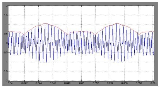
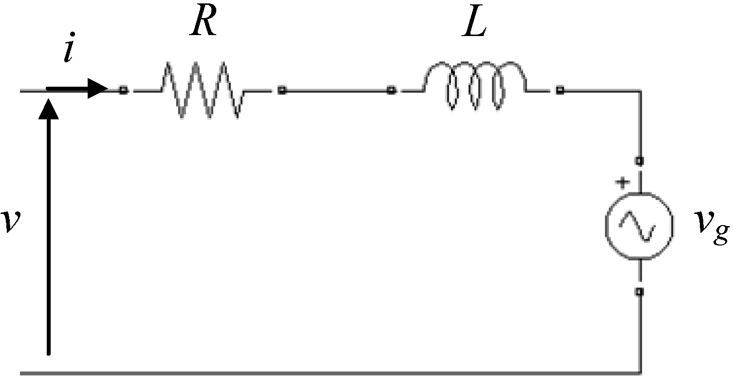
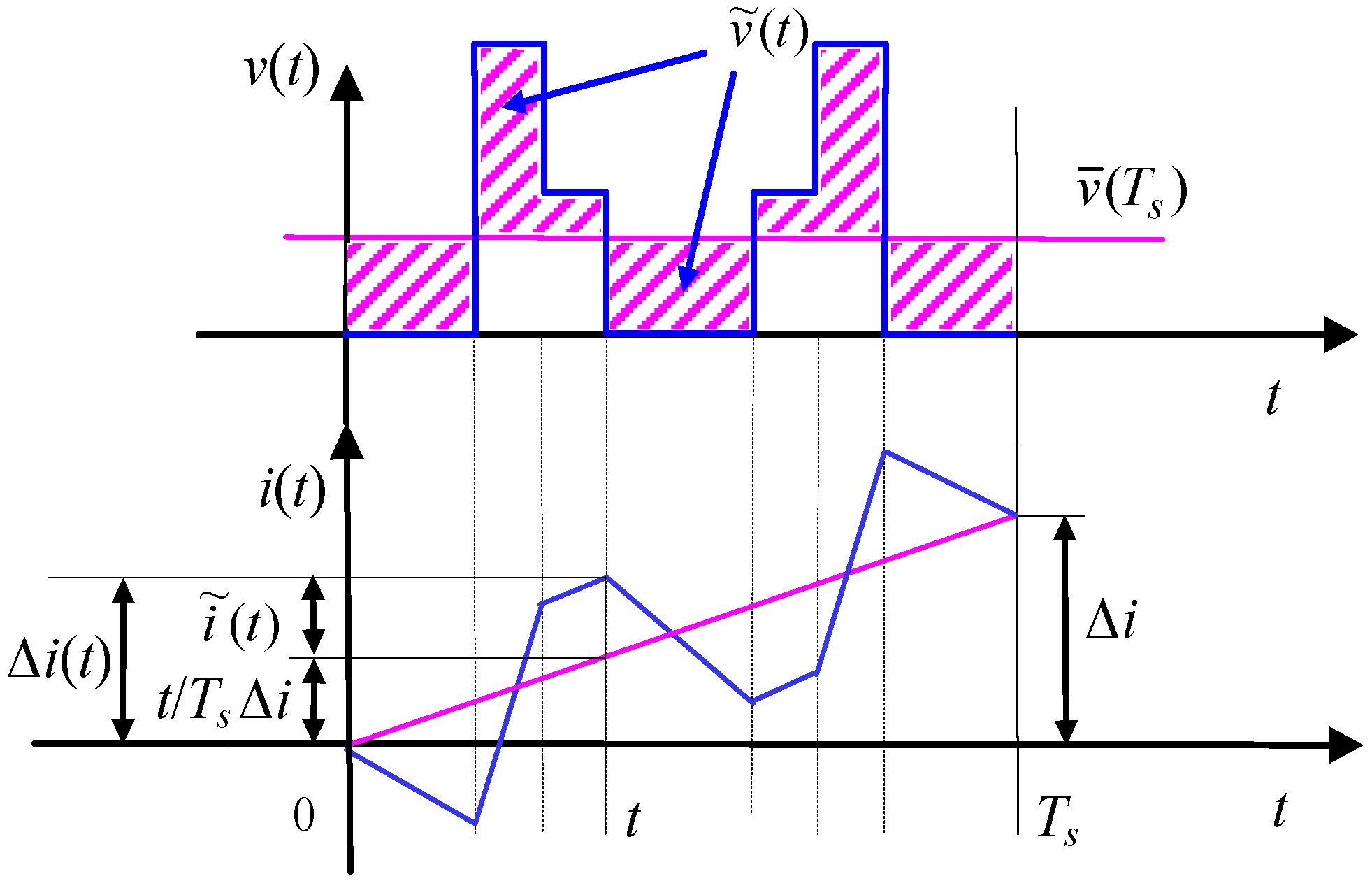
2.1. Load Model and Current Ripple Definitions

Basic RLE circuit scheme for a 7-phase balanced load is represented in Figure 1. The voltage equation can be written for each phase as:
v ( t ) = R i ( t ) + L d i d t + v g ( t )
Figure 1. Basic RLE circuit model for one phase.
Energies 06 04429 g001
By averaging Equation (1) over the switching period Ts leads to:
v ¯ ( T s ) = R i ¯ ( T s ) + L Δ i T s + v ¯ g ( T s )
being:
i = i(Ts) – i(0)
The alternating component of inverter voltage can be written by introducing the average over the switching period as:
v ˜ ( t ) = v ( t ) v ¯ ( T s )
By introducing Equations (1) and (2) in Equation (4) leads to:
v ˜ ( t ) = R [ i ( t ) i ¯ ( T s ) ] + L [ d i d t Δ i T s ] + [ v g ( t ) v ¯ g ( T s ) ]
The alternating voltage component has amplitude in the order of Vdc, as shown in Figure 2 (specific values of voltage levels for the 7-phase VSI are given below in Figure 5 and Figure 6).
Figure 2. Details of a generic output voltage and current ripple in the switching period.
Energies 06 04429 g002
The first term on the right side in Equation (5) accounts for the resistive voltage drop of the current ripple, that is much lower than the rated current in our analysis. The third (last) term in Equation (5) is the deviation of the generator’s actual voltage from its average value in the switching period, that is negligible if vg(t) is almost sinusoidal. For these reasons, the expression of alternating voltage component can be simplified as:
v ˜ ( t ) L [ d i d t Δ i T s ]
The current variation in sub-period [0–t], also depicted in Figure 2, can be calculated from Equation (6) as:
Δ i ( t ) 1 L 0 t v ˜ ( t ) d t + t T s Δ i
Equation (7) allows defining the instantaneous current ripple as:
i ˜ ( t ) = Δ i ( t ) t T s Δ i 1 L 0 t v ˜ ( t ) d t
Finally, the peak-to-peak current ripple amplitude can be calculated as:
i ˜ p p = m a x { i ˜ ( t ) } 0 T s m i n { i ˜ ( t ) } 0 T s

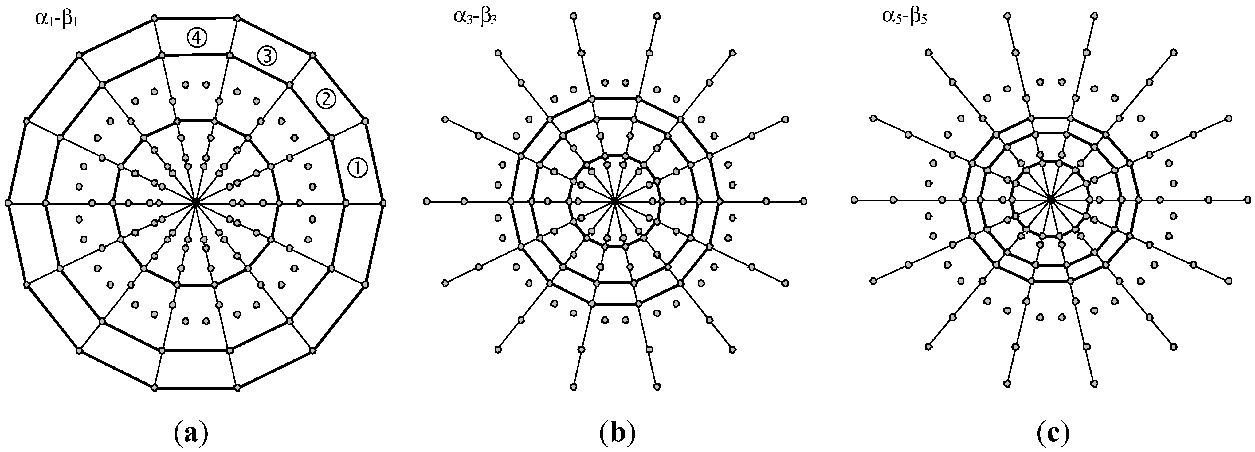
2.2. Multiple Space Vectors and PWM Equations

Multiple space vectors are introduced to represent voltage and current phase quantities in multiphase systems [5]. For the 7-phase system {x1, x2, x3, x4, x5, x6, x7}, the three space vectors x1, x3, and x5 lie in the three planes α1–β1, α3–β3 and α5–β5, respectively, and are expressed as:
{ x 1 = 2 7 [ x 1 + x 2 α + x 3 α 2 + x 4 α 3 + x 5 α 4 + x 6 α 5 + x 7 α 6 ] x 3 = 2 7 [ x 1 + x 2 α 3 + x 3 α 6 + x 4 α 2 + x 5 α 5 + x 6 α + x 7 α 4 ] x 5 = 2 7 [ x 1 + x 2 α 5 + x 3 α 3 + x 4 α + x 5 α 6 + x 6 α 4 + x 7 α 2 ] x 0 = 1 7 [ x 1 + x 2 + x 3 + x 4 + x 5 + x 6 + x 7 ]
being α = e(j 2π/7) and x0 the zero-sequence component, always null in case of balanced systems.
The inverse transformation of Equation (10) is:
x k = x 0 + x 1 α ( k 1 ) + x 3 α 3 ( k 1 ) + x 5 α 5 ( k 1 ) ,   k   1 ,   2 ,   ,   7
With reference to a 7-phase VSI supplied by the DC voltage Vdc, the output space voltage vectors can be written as function of the 7 switching leg states Sk = [0,1] as:
{ v 1 = 2 7 V d c [ S 1 + S 2 α + S 3 α 2 + S 4 α 3 + S 5 α 4 + S 6 α 5 + S 7 α 6 ] v 3 = 2 7 V d c [ S 1 + S 2 α 3 + S 3 α 6 + S 4 α 2 + S 5 α 5 + S 6 α + S 7 α 4 ] v 5 = 2 7 V d c [ S 1 + S 2 α 5 + S 3 α 3 + S 4 α + S 5 α 6 + S 6 α 4 + S 7 α 2 ]
The space vector diagrams representing all possible switch configurations on planes α1–β1, α3–β3 and α5–β5 are given in Figure 3.
Figure 3. Space vector diagrams of inverter output voltage in the planes (a) α1–β1; (b) α3–β3; and (c) α5–β5.
Energies 06 04429 g003
The SV-PWM of 7-phase inverters is based on the determination of application times of active and null inverter voltage vectors v1, v3, and v5 in every switching period Ts. In the case of symmetrical SV-PWM, the sequence is determined in Ts/2 and it is repeated symmetrically in the next half of the switching period [10]. By equally sharing the application time of the zero voltage vector between the null switch configurations 0000000 and 1111111, the so-called “centered” switching pattern is realized and a nearly-optimal modulation able to minimize the RMS of current ripple is obtained, as in the case of 3-phase [28] and 5-phase inverters [15]. This SV-PWM provides the same switching pattern such as the CB-PWM when a “min/max centering” common-mode voltage is injected into the modulating signals [10,29]. As result of the SV-PWM, for each phase, the average of the inverter output voltage v ¯ ( T s ) corresponds to the reference voltage v*.
In the case of sinusoidal balanced output voltages supplying a balanced load, the zero-sequence component is null. Introducing the modulation index m = V*/Vdc the reference space voltage vectors become:
{ v 1 * = v * = m V d c e j θ v 3 * = 0 v 5 * = 0
In this case, SVM is quarter-wave symmetric, and it can be analyzed in the range [0, π/2] of the phase angle θ= ωt. With reference to [Figure 4], the three sectors ①, ②, and ③ are considered for 0 ≤ θ ≤ π/7, π/7 ≤ θ ≤ 2π/7, and 2π/7 ≤ θ ≤ 3π/7, respectively, and the half of sector ④ is considered for 3π/7 ≤ θ ≤ π/2.
Figure 4. Space vector diagram of inverter output voltage on plane α1–β1 in the range θ = [0, 90°]. Outer dashed circle is modulation limit, mmax ≈ 0.513. Different colored areas correspond to different equations for determining the current ripple.
Energies 06 04429 g004
For sector ① the application times of the switch configurations involved in the modulation sequence from {00} to {7F} (hexadecimal) can be determined in the half period Ts/2 as [10]:
t 1 = m T s K 1 s i n ( π / 7 θ ) ,   100 0000 = { 40 }
t 2 = m T s K 5 s i n θ ,   110 0000 = { 60 }
t 3 = m T s K 3 s i n ( π / 7 θ ) ,   110 0001 = { 61 }
t 4 = m T s K 3 s i n θ ,   111 0001 = { 71 }
t 5 = m T s K 5 s i n ( π / 7 θ ) ,   111 0011 = { 73 }
t 6 = m T s K 1 s i n θ ,   111 1011 = { 7 B }
t 0 = T s 2 ( t 1 + t 2 + t 3 + t 4 + t 5 + t 6 ) = 1 2 m ( K 1 + K 3 + K 5 ) [ K 1 c o s θ + ( 1 c o s π 7 ) s i n θ ] ( 000 0000 111 1111 ) = { 00 7 F }
being:
{ K 1 = s i n π 7 0.434 K 3 = s i n 3 π 7 0.975 K 5 = s i n 5 π 7 0.782
Equations (14–20) can be extended to any sector k by replacing the phase angle θ with θ − (k−1)π/7, k = 1, 2, …, 14.
Note that the modulation limit is mmmax ≈ 0.513, according to the generalized expression given in [30] for n phases, mmax = [2cos(π/2n)]−1.

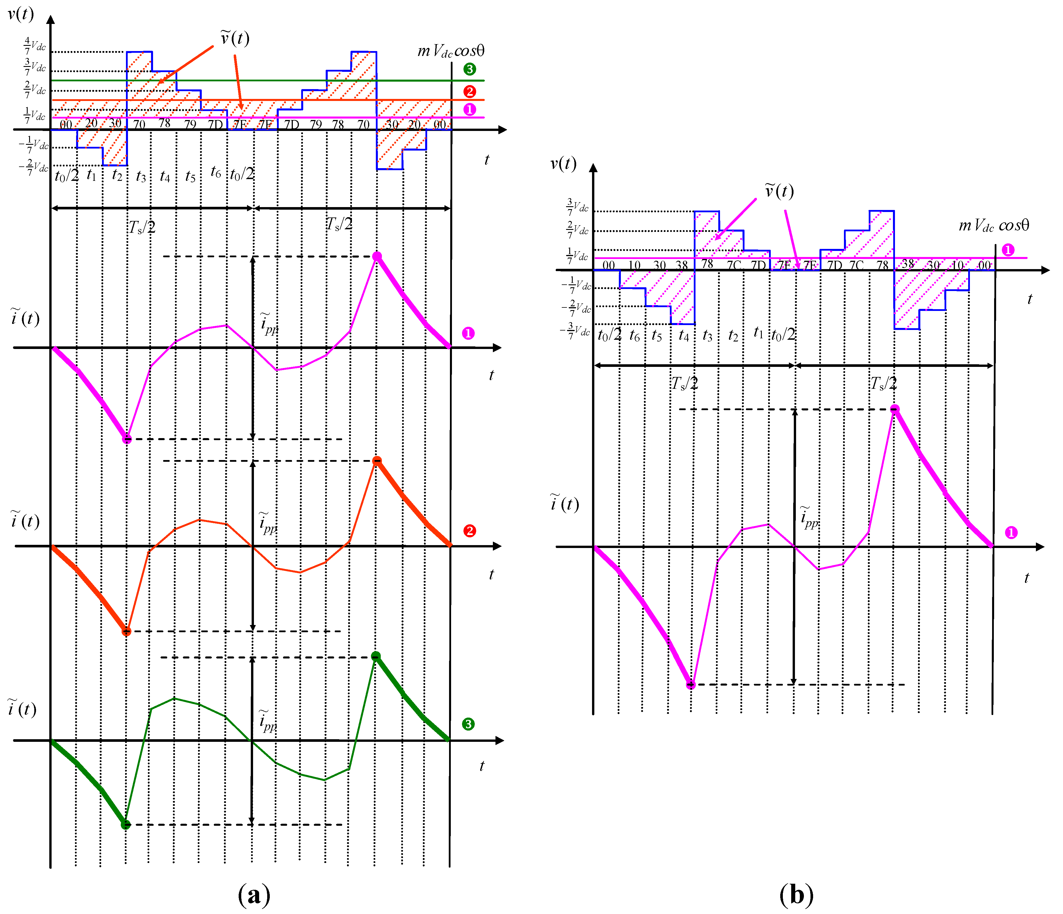
2.3. Ripple Evaluation

Due to the symmetry among all phases in the considered case of sinusoidal balanced currents, only the first phase is examined in the following analysis. In terms of multiple space vectors, the phase variables are given by Equation (11). For the first phase, it results in the projection of the three space vectors on the real axes. In particular, introducing Equations (13) in (11), the average output voltage of the first phase is given by:
v ¯ ( T s ) = v * = e { v 1 * } + e { v 3 * } + e { v 5 * } = m V d c cos θ
By introducing Equation (22) in Equation (4), and calculating v(t) by Equations (11) and (12), the alternating component of inverter output voltage (first phase) can be written as:
v ˜ ( t ) = [ S 1 1 7 ( S 1 + S 2 + S 3 + S 4 + S 5 + S 6 + S 7 ) ] V d c m V d c c o s θ
In order to evaluate the current ripple in the whole phase angle range 0 < θ < π/2, the four main cases corresponding to the four sectors depicted in Figure 4 should be considered. Additional sub-cases, also determined by the value of modulation index, are identified in Figure 4 with different colored areas.
The current ripple for each sector is depicted in a separate diagram, Figure 5 and Figure 6. In general, for all the four sectors, the ripple shows two different peaks in the switching period (two positive peaks and the symmetric negative peaks). In most of these cases, one peak results to be always bigger than the other in the considered sector, for any specific range of mcosθ, as a consequence of both current slopes and application times. There are only two exceptions, that are both related to the second sector ②. For these cases, either one or the other peak is bigger depending on the values of m and θ. These aspects are addressed with more details in the following section.

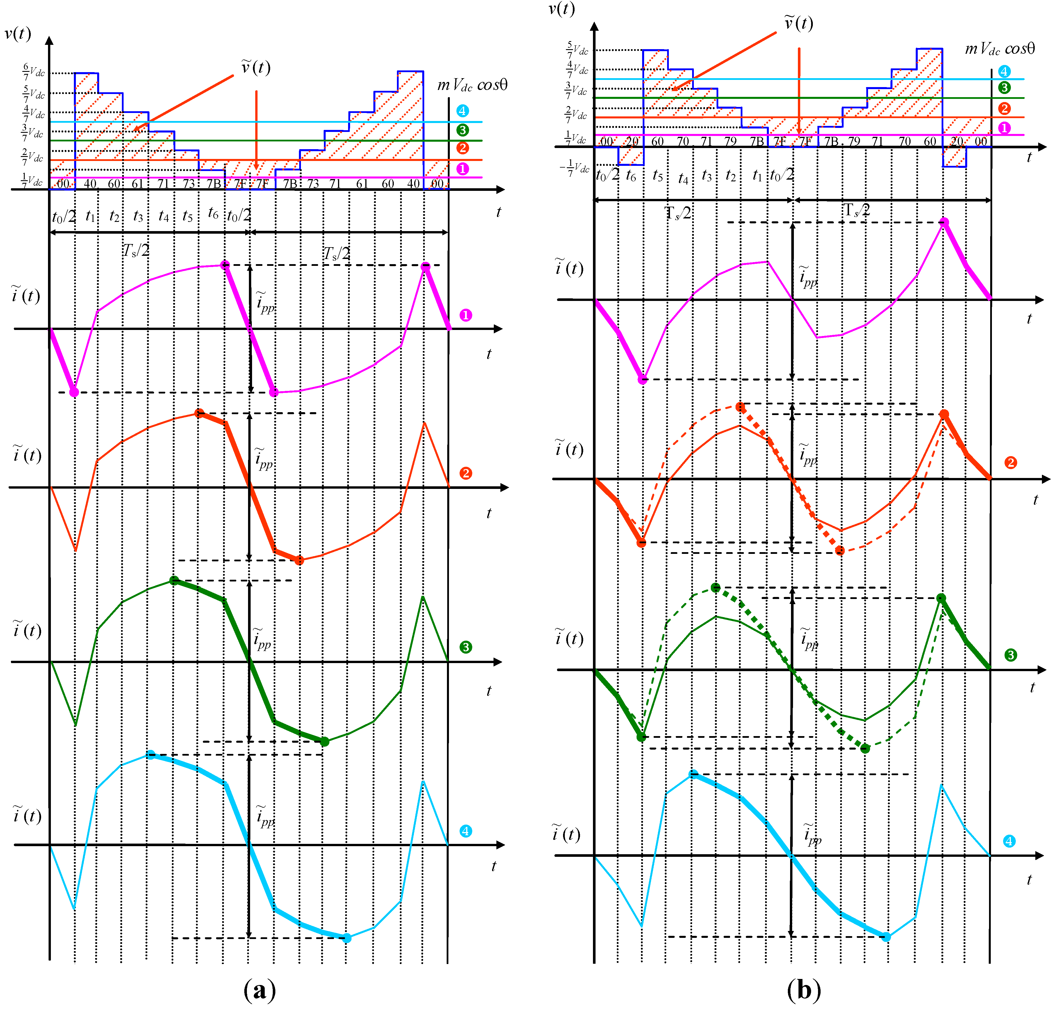
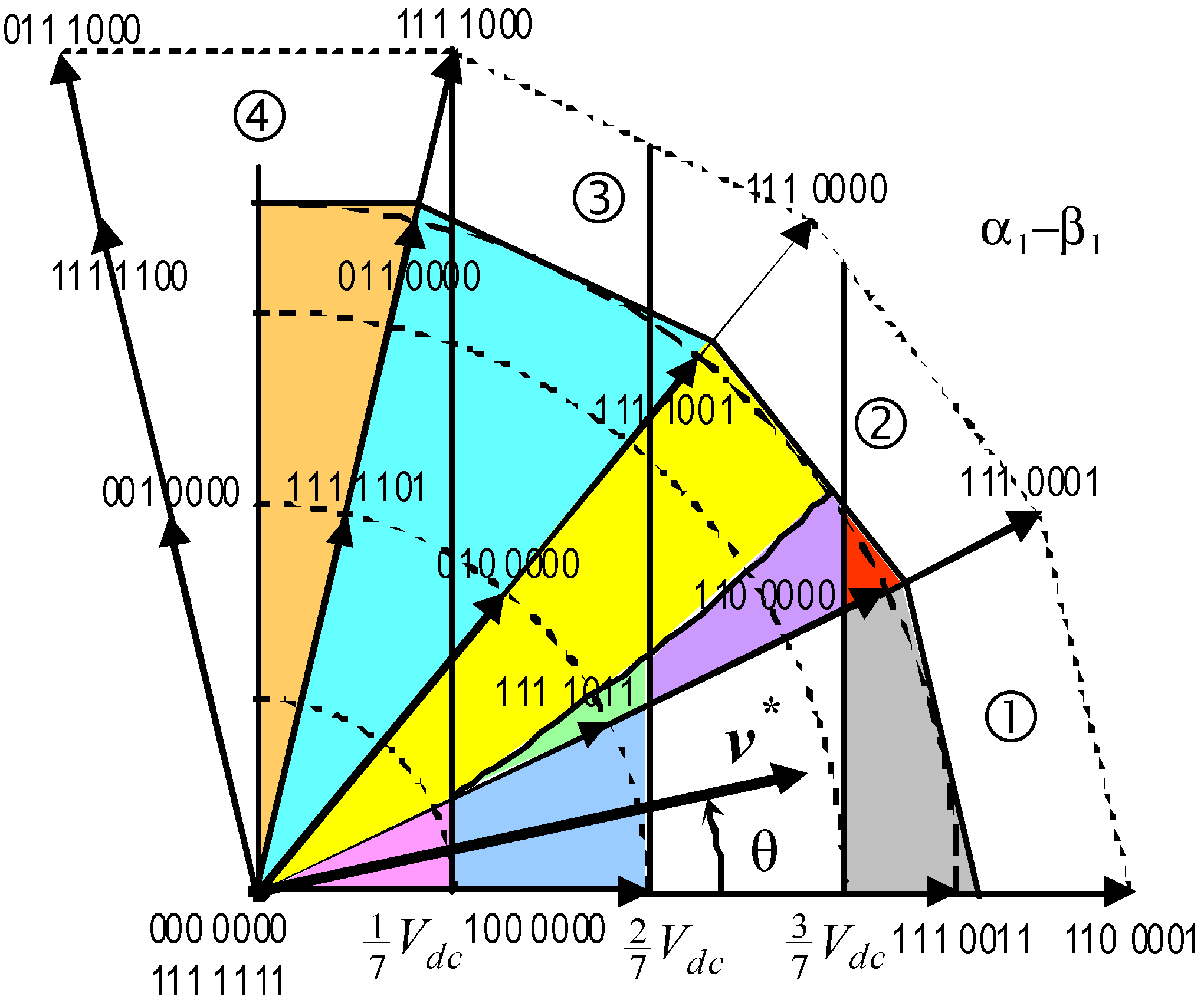
2.3.1. Evaluation in the First Sector

Considering sector ①, 0 ≤ θ ≤ π/7, four different sub-cases can be distinguished: 0 ≤ mcosθ ≤ 1/7, 1/7 ≤ mcosθ ≤ 2/7, 2/7 ≤ mcosθ ≤ 3/7, and 3/7 ≤ mcosθ ≤ mmaxcosθ < 4/7. All this sub-cases are represented in Figure 5a.
The sub-case 0 ≤ mcosθ ≤ 1/7 (pink area in Figure 4) is considered in diagram ➊ of Figure 5a, where the current ripple i ˜ and its peak-to-peak value i ˜ p p are depicted, together with the instantaneous output voltage v(t). In this case, according to Figure 5a, i ˜ p p can be evaluated by Equations (8), (9) and (23) considering the switch configurations {00} or {7F} with the corresponding application interval t0, leading to:
i ˜ p p = 1 L { m V d c c o s θ t 0 }
Figure 5. Output voltage and current ripple in a switching period. (a) For sector ①, 0 ≤ θ ≤ π/7; and (b) for sector ②, π/7 ≤ θ ≤ 2π/7.
Energies 06 04429 g005
Peak-to-peak current ripple can also be expressed as:
i ˜ p p = V d c T s 2 L r ( m , θ )
being r(m, θ) the normalized peak-to-peak current ripple amplitude. In this case, introducing the duty-cycle δ0 = t0/Ts/2:
r ( m , θ ) = m c o s θ δ 0
The sub-case 1/7 ≤ mcosθ ≤ 2/7 (azure area in Figure 4) is depicted in diagram ➋ of Figure 5a. In this case i ˜ p p can be evaluated considering the switch configurations {7F} and {7B}, with the corresponding application intervals t0/2 and t6, leading to:
i ˜ p p = 2 L { m V d c c o s θ t 0 2 + ( m V d c c o s θ V d c 7 ) t 6 }
Normalizing by Equation (25) and introducing the duty-cycles δk = tk/Ts/2, the normalized current ripple becomes:
r ( m , θ ) = m c o s θ δ 0 + 2 ( m c o s θ 1 7 ) δ 6
The sub-case 2/7 ≤ mcosθ ≤ 3/7 (white area in Figure 4) is depicted in diagram ➌ of Figure 5a. In this case i ˜ p p can be evaluated considering the switch configurations {7F}, {7B}, and {73} with the corresponding application intervals t0/2, t6, and t5, leading to:
i ˜ p p = 2 L { m V d c cos θ t 0 2 + ( m V d c cos θ V d c 7 ) t 6 +   ( m V d c cos θ 2 V d c 7 ) t 5 }
The corresponding normalized current ripple is:
r ( m , θ ) = m cos θ δ 0 + 2 ( m cos θ 1 7 ) δ 6 +   2 ( m cos θ 2 7 ) δ 5
The sub-case 3/7 ≤ mcosθ ≤ mmaxcosθ <4/7 (gray area in Figure 4) is depicted in diagram ➍ of Figure 5a. In this case i ˜ p p can be evaluated considering the switch configurations {7F}, {7B}, {73}, and {71} with the corresponding application intervals t0/2, t6, t5, and t4, leading to:
i ˜ p p = 2 L { m V d c c o s θ t 0 2 + ( m V d c c o s θ V d c 7 ) t 6 +   ( m V d c c o s θ 2 V d c 7 ) t 5 +   ( m V d c c o s θ 3 V d c 7 ) t 4 }
The corresponding normalized current ripple is:
r ( m , θ ) = m c o s θ δ 0 + 2 ( m c o s θ 1 7 ) δ 6 + 2 ( m c o s θ 2 7 ) δ 5 + 2 ( m c o s θ 3 7 ) δ 4

2.3.2. Evaluation in the Second Sector

Considering sector ②, π/7 ≤ θ ≤ 2π/7, four different sub-cases can be identified: 0 ≤ mcosθ ≤ 1/7, 1/7 ≤ mcosθ ≤ 2/7, 2/7 ≤ mcosθ ≤ 3/7, and 3/7 ≤ mcosθ ≤ mmaxcosθ < 4/7. All these sub-cases are represented in Figure 5b.
The sub-case 0 ≤ mcosθ ≤ 1/7 (yellow area in Figure 4) is depicted in diagram ➊ of Figure 5b. According to this figure, i ˜ p p can be evaluated by Equations (8), (9) and (23) considering the switch configurations {00} and {20} with the corresponding application intervals t0/2 and t6:
i ˜ p p = 2 L { m V d c c o s θ   t 0 2 + ( m V d c c o s θ + 1 7 V d c ) t 6 }
Normalizing by Equation (25) and introducing the duty-cycles, the normalized peak-to-peak current ripple amplitude becomes:
r ( m , θ ) = m c o s θ   δ 0 + 2 ( m c o s θ + 1 7 ) δ 6
The sub-case 1/7 ≤ mcosθ ≤ 2/7 is depicted in diagram ➋ of Figure 5b. It can be noticed that there are two possible situations regarding the evaluation of i ˜ p p , corresponding to yellow-green area of sector ② in Figure 4:
  • In the first situation, yellow area (solid orange line in Figure 5b), i ˜ p p can be determined as in the previous sub-case by considering the switch configurations {00} and {20} with the corresponding application intervals t0/2 and t6, leading to Equations (33) and (34);
  • In the second situation, green area (dashed orange line in Figure 5b), i ˜ p p can be determined by considering the switch configurations {7F} and {7B} with the corresponding application intervals t0/2 and t1, leading to:
    i ˜ p p = 2 L { m V d c c o s θ   t 0 2 + ( m V d c c o s θ 1 7 V d c ) t 1 }
being the normalized peak-to-peak current ripple amplitude:
r ( m , θ ) = m c o s θ   δ 0 + 2 ( m c o s θ 1 7 ) δ 1
The sub-case 2/7 ≤ mcosθ ≤ 3/7 is depicted in diagram ➌ of Figure 5b. Also for this sub-case there are two possible situations for evaluating, i ˜ p p corresponding to yellow-violet area of sector ② in Figure 4:
  • In the first situation, yellow area (solid green line in Figure 5b), i ˜ p p can be determined as in the previous sub-case by considering the switch configurations {00} and {20} with the corresponding application intervals t0/2 and t6, leading to Equations (33) and (34);
  • In the second situation, violet area (dashed green line in Figure 5b), i ˜ p p can be determined by considering the switch configurations {7F}, {7B}, and {79}, with the corresponding application intervals t0/2, t1, and t2, leading to:
    i ˜ p p = 2 L { m V d c c o s θ t 0 2 + ( m V d c c o s θ V d c 7 ) t 1 + ( m V d c c o s θ 2 V d c 7 ) t 2 }
Normalized current ripple is:
r ( m , θ ) = m c o s θ δ 0 + 2 ( m c o s θ 1 7 ) δ 1 +   2 ( m c o s θ 2 7 ) δ 2
The last sub-case 3/7 ≤ mcosθ ≤ mmaxcosθ <4/7 (red area in Figure 4) is depicted in diagram ➍ of Figure 5b. According to this figure, i ˜ p p can be evaluated considering the switch configurations {7F}, {7B}, {79}, and {71} with the corresponding application intervals t0/2, t1, t2, and t3, leading to:
i ˜ p p = 2 L { m V d c c o s θ t 0 2 + ( m V d c c o s θ V d c 7 ) t 1 +   ( m V d c c o s θ 2 V d c 7 ) t 2 +   ( m V d c c o s θ 3 V d c 7 ) t 3 }
Normalized current ripple is:
r ( m , θ ) = m c o s θ δ 0 + 2 ( m c o s θ 1 7 ) δ 1 + 2 ( m c o s θ 2 7 ) δ 2 + 2 ( m c o s θ 3 7 ) δ 3

2.3.3. Evaluation in the Third Sector

With reference to sector ③, 2π/7 ≤ θ ≤ 3π/7 (turquoise area in Figure 4), three different ranges can be distinguished: 0 ≤ mcosθ ≤ 1/7, 1/7 ≤ mcosθ ≤ 2/7, and 2/7 ≤ mcosθ ≤ mmaxcosθ < 3/7, represented in diagrams ➊, ➋, ➌ of Figure 6a. It can be noted that there are not sub-cases, and for all the three ranges i ˜ p p can be evaluated considering the switch configurations {00}, {20}, and {30} with the corresponding application intervals t0, t1, and t2, leading to:
i ˜ p p = 2 L { m V d c c o s θ t 0 2 + ( m V d c c o s θ + V d c 7 ) t 1 + ( m V d c c o s θ + 2 V d c 7 ) t 2 }
Normalized current ripple is:
r ( m , θ ) = m c o s θ δ 0 + 2 ( m c o s θ + 1 7 ) δ 1 +   2 ( m c o s θ + 2 7 ) δ 2
Figure 6. Output voltage and current ripple in a switching period. (a) For sector ③, 2π/7 ≤ θ ≤ 3π/7; and (b) for sector ④, 3π/7 ≤ θ ≤ π/2.
Energies 06 04429 g006

2.3.4. Evaluation in the Fourth (Half) Sector

With reference to the half of sector ④, 3π/7 ≤ θ ≤ π/2 (orange area in Figure 4), there are not sub-cases and the only occurrence is 0 ≤ mcosθ ≤ mmaxcosθ < 1/7, as depicted in Figure 6b. In this case, i ˜ p p can be evaluated considering the switch configurations {00}, {10}, {30}, and {38} with the corresponding application interval t0/2, t6, t5, and t4, leading to:
i ˜ p p = 2 L { m V d c c o s θ t 0 2 + ( m V d c c o s θ + V d c 7 ) t 6 + ( m V d c c o s θ + 2 V d c 7 ) t 5 +   ( m V d c c o s θ + 3 V d c 7 ) t 4 }
The corresponding normalized current ripple is:
r ( m , θ ) = m c o s θ δ 0 + 2 ( m c o s θ + 1 7 ) δ 6 + 2 ( m c o s θ + 2 7 ) δ 5 + 2 ( m c o s θ + 3 7 ) δ 4

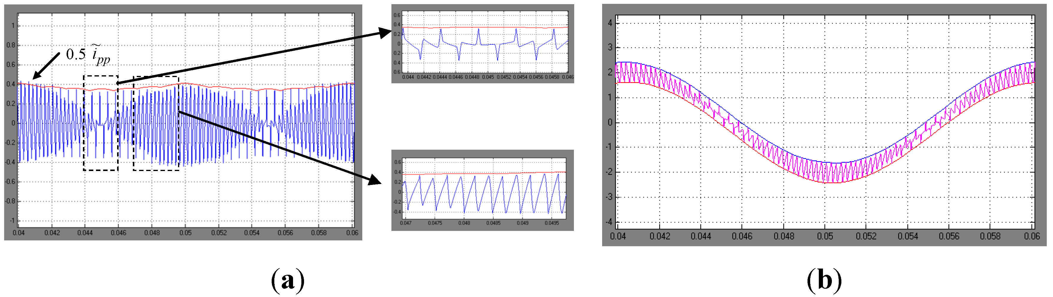
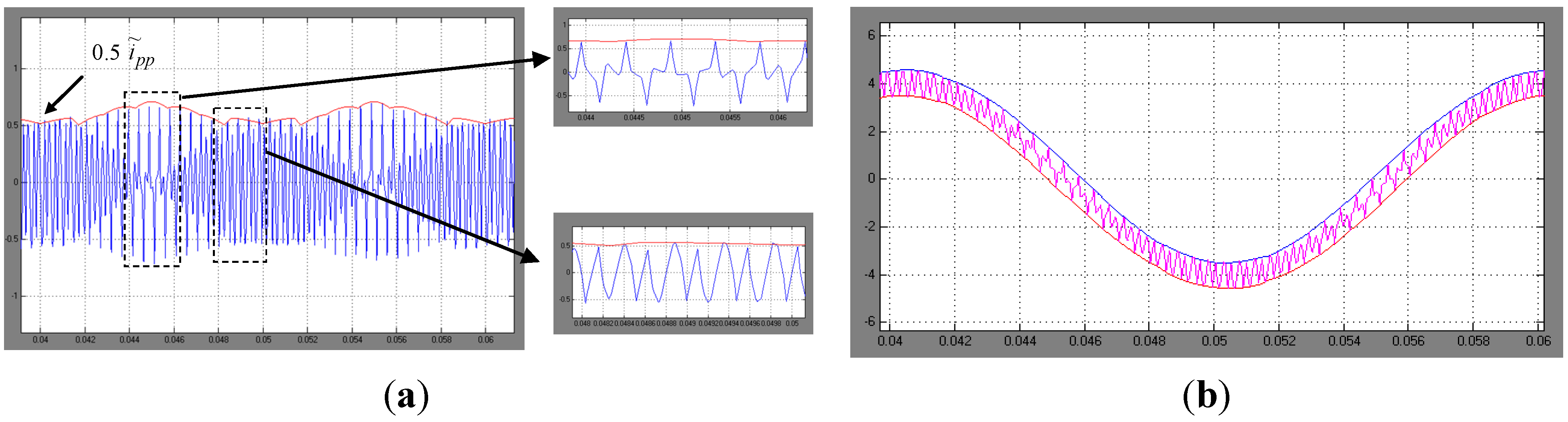
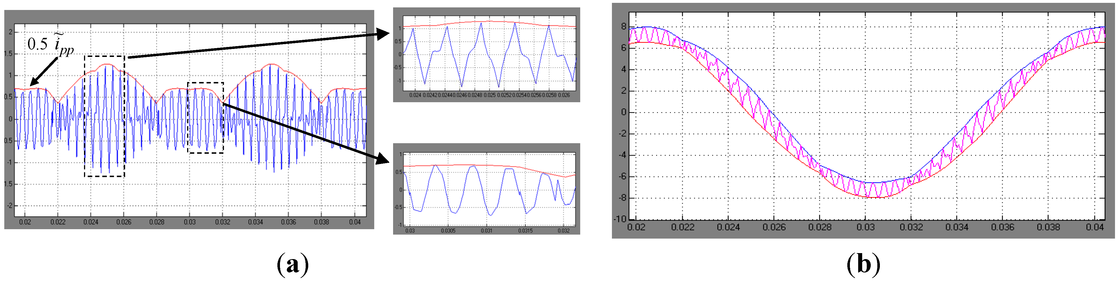
2.4. Peak-to-Peak Current Ripple Diagrams

In order to show the behavior of the peak-to-peak current ripple amplitude in the fundamental period for all the considered cases, in Figure 7a,b is represented the normalized function r(m, θ) defined by Equation (25). Figure 7a shows r(θ) for m = 1/7, 2/7, 3/7, and 0.513 (≈mmax), corresponding to the dashed circles in Figure 4. The four ranges corresponding to the four sectors from ① to ④ are emphasized. The further sub-regions in sector ② (green-, violet-, and red-colored areas in Figure 4) can be distinguished for m = 2/7 and 3/7.Figure 7b shows the colored map of r(m, θ) for the first quadrant within the modulation limits. It can be noted that ripple amplitude is obviously zero for m = 0, since the null configurations are the only applied, increasing almost proportionally with m in the neighborhoods of m = 0. A phase angle with minimum ripple can be indentified in the range θ ≈ 30°/35°. A phase angle with maximum ripple is θ = 90°, with ripple amplitude proportional to modulation index: r(m, 90°) = 0.626 m, resulting from Equation (44). This aspect is further developed in the following sub-section.
Figure 7. Diagrams of the normalized peak-to-peak current ripple amplitude r(m, θ). (a) As a function of the phase angle θ in the range [0, π/2], for different modulation indexes; and (b) colored map in the space vector plane α–β within the modulation limits.
Energies 06 04429 g007

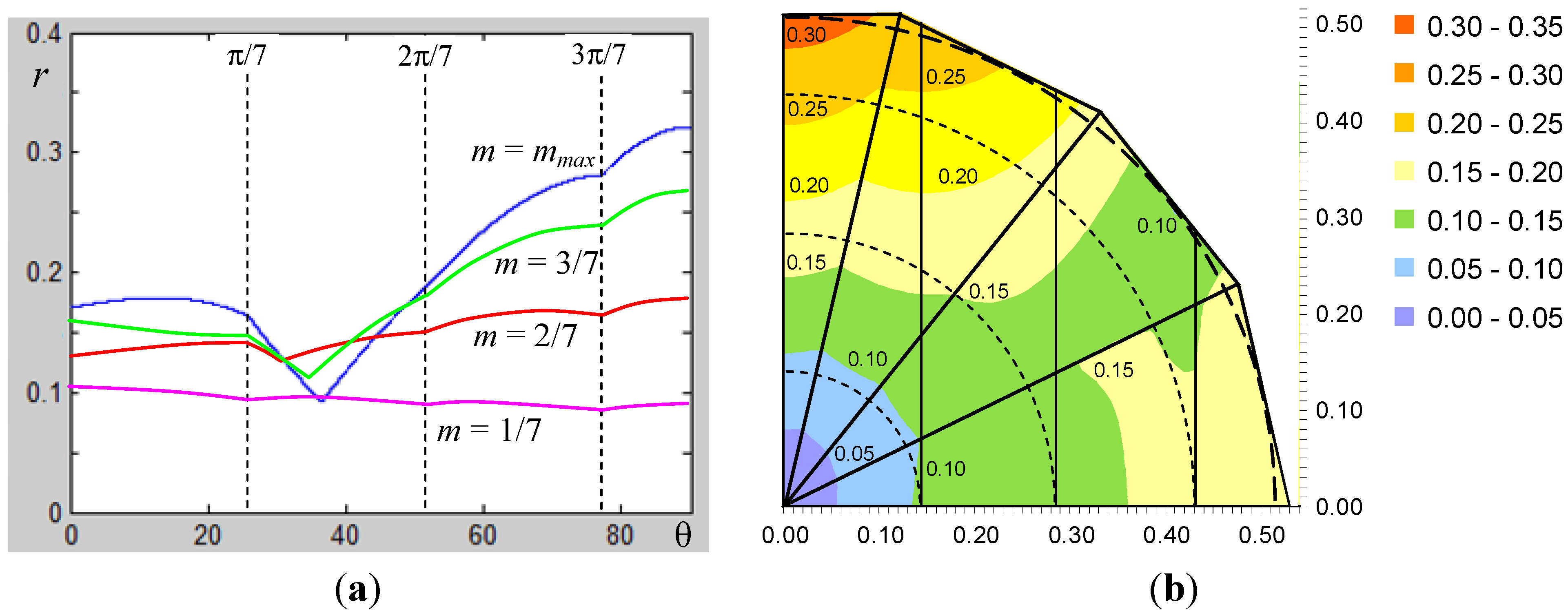
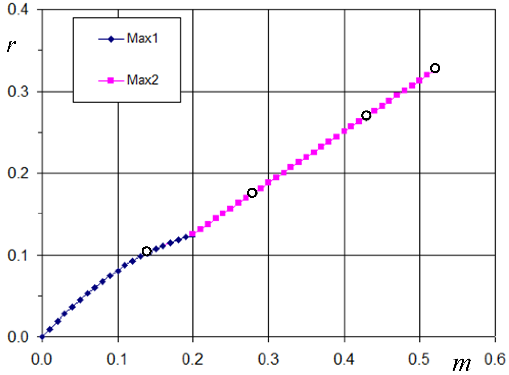
2.5. Maximum of the Current Ripple

In order to estimate the current ripple amplitude in the whole fundamental period, the maximum of the current ripple can be evaluated in the phase angle range [0, 90°]. For this purpose, two relevant angles can be observed in Figure 7a,b: a local maximum is for θ = 0, and a further local maximum is for θ = 90°. In particular, to determine these two local maxima, θ = 0 can be set in Equation (26), and θ = 90° in Equation (44), introducing the application times given by Equations (14–20). The maximum value of normalized peak-to-peak current ripple amplitude as a function of the modulation index becomes:
r m a x ( m ) = m a x { m [ 1 2 m K 1 2 2 m K 1 K 3 2 m K 1 K 5 ] ,   0.626 m }
The intersection between the two local maxima gives the border value of the modulation index:
m [ 1 2 m K 1 2 2 m K 1 K 3 2 m K 1 K 5 ] = 0.626 m
leading to m ≈ 0.197. Finally, combining Equations (45) and (46), the maximum of the normalized current ripple is:
r m a x ( m )   =   { m [ 1 2 m K 1 2 2 m K 1 K 3 2 m K 1 K 5 ] ,   m   0.197 0.626 m    ,   m   0.197 .
The composition of the two local maxima is given in Figure 8, leading to the global maximum. The four white dots represent the specific modulation indexes, m = 1/7, 2/7, 3/7, and 0.513 (≈mmax), also displayed in Figure 7a and further examined in simulations. It can be noted that maximum function is almost linear with the modulation index, strictly for m > 0.197. Then, on the basis of Equations (47) and (25), a simplified expression for maximum of peak-to-peak current ripple amplitude is obtained for the 7-phase inverter:
i ˜ p p m a x     V d c T s 3.2 L m
Figure 8. Maximum of the normalized peak-to-peak current ripple amplitude as function of modulation index.
Energies 06 04429 g008

3. Numerical Results

In order to verify the theoretical developments shown in previous sections, circuit simulations are carried out by Sim-PowerSystems of Matlab (The MathWorks, Natick, MA, USA) considering seven-phase inverter supplying a balanced RL load, having R = 7 Ω and L = 3 mH.
In all simulations the fundamental frequency f is set to 50 Hz, the switching frequency 1/Ts is 2.1 kHz, and the DC voltage supply Vdc is 100 V. A centered symmetrical carrier-based PWM technique is considered, equivalent to the multiple space vector PWM presented in Section 2.2.
The 14 power transistors have been modeled with ideal switches, expecting a very precise matching with the analytical developments. By introducing non idealities in simulations, such as commutation times, voltage drops, parasitic elements, deadtimes etc, leads to output voltage distortion with additional harmonics [31], making more difficult the validation of the proposed theoretical approach.
The instantaneous current ripple i ˜ is calculated as the difference between the instantaneous current i(t) and its fundamental component Ifund(t), i.e.,:
i ˜ ( t ) = i ( t ) I f u n d ( t )
The 7-phase system is well balanced and the first phase is selected for further analysis, as in analytical developments. Different values of m are investigated (1/7, 2/7 3/7, and 0.513 ≈ mmax), as in Section 2, to cover all the considered cases.
In Figure 9a, Figure 10a, Figure 11a, and Figure 12a the current ripple i ˜ calculated in simulations by Equation (49) (blue trace) is compared with the half of peak-to-peak current ripple, i ˜ p p / 2 , evaluated in the different regions by the equations presented in Section 2.3 (red trace), for one fundamental period. Each figure is backed with the enlarged detailed view of the current ripple.
In the corresponding Figure 9b, Figure 10b, Figure 11b, and Figure 12b is depicted the instantaneous output current with the calculated upper/lower ripple envelope, depicted in blue/red colors, respectively.
The agreement is good in the whole fundamental period. Shown figures (Figure 9 to Figure 12) are for modulation indexes that cover all possible sub-cases, i.e., all the colored regions in Figure 4. This proves the validity of all the equations derived in Section 2.3.
Figure 9. (a) Current ripple for m = 1/7. Simulation results (blue) and evaluated peak-to-peak amplitude (red envelope) for one fundamental period, with details; (b) instantaneous output current with calculated ripple envelopes (red and blue traces).
Energies 06 04429 g009
Figure 10. (a) Current ripple for m = 2/7. Simulation results (blue) and evaluated peak-to-peak amplitude (red envelope) for one fundamental period, with details; (b) instantaneous output current with calculated ripple envelopes (red and blue traces).
Energies 06 04429 g010
Figure 11. (a) Current ripple for m = 3/7. Simulation results (blue) and evaluated peak-to-peak amplitude (red envelope) for one fundamental period, with details; (b) instantaneous output current with calculated ripple envelopes (red and blue traces).
Energies 06 04429 g011
Figure 12. Current ripple for m= 0.513 (≈mmax). (a) Simulation results (blue) and evaluated peak-to-peak amplitude (red envelope) for one fundamental period, with details; (b) instantaneous output current with calculated ripple envelopes (red and blue traces).
Energies 06 04429 g012

4. Conclusions

In this paper the instantaneous output current ripple for seven-phase PWM inverters has been identified and analyzed in details. In particular, the analytical expression of peak-to-peak current ripple amplitude has been derived in the whole fundamental period as function of the modulation index by identifying four different relevant cases and some sub-cases.
Furthermore, a simplified expression to evaluate maximum of the current ripple amplitude in the fundamental period is given. In particular, it has been pointed out that maximum peak-to-peak current ripple amplitude is almost linear function of the modulation index. The analytical developments have been verified with numerical simulations with reference to all the considered cases by a realistic inverter-load circuit model.
Despite of the proposed method is applied to centered symmetrical PWM, the analysis can be readily extended to either discontinuous or asymmetrical modulation, both carrier-based and space vector PWM. Furthermore, the derived analytical expressions can be utilized to minimize the current ripple amplitude by properly adjusting the switching frequency and/or by modifying the sharing of the application time of the zero voltage vector between the two null switch configurations. This could be the topic of further investigations.

Acknowledgments

The authors would like to thank the Institute of Advanced Studies (ISA) of the University of Bologna, Italy, for the support.

Conflicts of Interest

The authors declare no conflict of interest.

References

  1. Toliyat, H.A.; Waikar, S.P.; Lipo, T.A. Analysis and simulation of five-phase synchronous reluctance machines including third harmonic of airgap MMF. IEEE Trans. Ind. Appl. 1998, 34, 332–339. [Google Scholar] [CrossRef]
  2. Xu, H.; Toliyat, H.A.; Petersen, L.J. Five-phase induction motor drives with DSP-based control system. IEEE Trans. Power Electron. 2002, 17, 524–533. [Google Scholar] [CrossRef]
  3. Ryu, H.M.; Kim, J.K.; Sul, S.K. Synchronous Frame Current Control of Multi-Phase Synchronous Motor: Part I. Modeling and Current Control based on Multiple d-q Spaces Concept under Balanced Condition. In Proceedings of the 39th Annual Meeting of IEEE Industry Application Society, Seattle, WA, 3–7 October 2004; pp. 56–63.
  4. Parsa, L.; Toliyat, H.A. Five-phase permanent-magnet motor drives. IEEE Trans. Ind. Appl. 2005, 41, 30–37. [Google Scholar] [CrossRef]
  5. Grandi, G.; Serra, G.; Tani, A. General Analysis of Multi-Phase Systems based on Space Vector Approach. In Proceedings of 12th Power Electronics and Motion Control Conference (EPE-PEMC), Portoroz, Slovenia, 30 August–1 September 2006; pp. 834–840.
  6. Ryu, H.M.; Kim, J.W.; Sul, S.K. Analysis of multi-phase space vector pulse width modulation based on multiple d-q spaces concept. IEEE Trans. Power Electron. 2005, 20, 1364–1371. [Google Scholar] [CrossRef]
  7. Iqbal, A.; Levi, E. Space Vector Modulation Schemes for a Five-Phase Voltage Source Inverter. In Proceedings of 11th European Conference on Power Electronics and Applications (EPE), Dresden, Germany, 11–14 September 2005; pp. 1–12.
  8. De Silva, P.S.N.; Fletcher, J.E.; Williams, B.W. Development of Space Vector Modulation Strategies for Five Phase Voltage Source Inverters. In Proceedings of Power Electronics, Machines and Drives Conference (PEMD), Edinburgh, UK, 31 March–2 April 2004; pp. 650–655.
  9. Ojo, O.; Dong, G. Generalized Discontinuous Carrier-Based PWM Modulation Scheme for Multi-Phase Converter-Machine Systems. In Proceedings of 40th Annual Meeting of IEEE Industry Applications Society, Hong Kong, China, 2–6 October 2005; pp. 1374–1381.
  10. Grandi, G.; Serra, G.; Tani, A. Space Vector Modulation of a Seven-Phase Voltage Source Inverter. In Proceedings of the International Symposium on Power Electronics, Electrical Drives, Automation and Motion (SPEEDAM), Taormina, Italy, 23–26 May 2006; pp. 1149–1156.
  11. Dujic, D.; Levi, E.; Serra, G.; Tani, A.; Zarri, L. General modulation strategy for seven-phase inverters with independent control of multiple voltage space vectors. IEEE Trans. Ind. Electron. 2008, 55, 1921–1932. [Google Scholar] [CrossRef]
  12. Dujic, D.; Levi, E.; Jones, M.; Grandi, G.; Serra, G.; Tani, A. Continuous PWM Techniques for Sinusoidal Voltage Generation with Seven-Phase Voltage Source Inverters. In Proceedings of the Power Electronics Specialists Conference (IEEE-PESC), Orlando, FL, USA, 17–21 June 2007; pp. 47–52.
  13. Hu, J.S.; Chen, K.Y.; Shen, T.Y.; Tang, C.H. Analytical solutions of multilevel space-vector PWM for multiphase voltage source inverters. IEEE Trans Power Electron. 2011, 26, 1489–1502. [Google Scholar] [CrossRef]
  14. Lopez, O.; Alvarze, J.; Gandoy, J.D.; Freijedo, F.D. Multiphase space vector PWM algorithm. IEEE Trans Ind. Electron. 2008, 55, 1933–1942. [Google Scholar] [CrossRef]
  15. Casadei, D.; Mengoni, M.; Serra, G.; Tani, A.; Zarri, L. A New Carrier-Based PWM Strategy with Minimum Output Current Ripple for Five-Phase Inverters. In Proceedings of the 14th European Conference on Power Electronics and Applications (EPE), Birmingham, UK, 30 August–1 September 2011; pp. 1–10.
  16. Dujic, D.; Jones, M.; Levi, E. Analysis of output current ripple rms in multiphase drives using space vector approach. IEEE Trans. Power Electron. 2009, 24, 1926–1938. [Google Scholar] [CrossRef]
  17. Jones, M.; Dujic, D.; Levi, E.; Prieto, J.; Barrero, F. Switching ripple characteristics of space vector PWM schemes for five-phase two-level voltage source inverters—Part 2: Current ripple. IEEE Trans. Ind. Electron. 2011, 58, 2799–2808. [Google Scholar] [CrossRef]
  18. Dahono, P.A.; Supriatna, E.G. Output current-ripple analysis of five-phase PWM inverters. IEEE Trans. Ind. Appl. 2009, 45, 2022–2029. [Google Scholar] [CrossRef]
  19. Dujic, D.; Jones, M.; Levi, E. Analysis of output current-ripple RMS in multiphase drives using polygon approach. IEEE Trans. Power Electron. 2010, 25, 1838–1849. [Google Scholar] [CrossRef]
  20. Jiang, D.; Wang, F. Study of Analytical Current Ripple of Three-Phase PWM Converter. In Proceedings of the 27th IEEE Applied Power Electronics Conference and Exposition (APEC), Orlando, FL, USA, 5–9 February 2012; pp. 1568–1575.
  21. Grandi, G.; Loncarski, J.; Seebacher, R. Effects of Current Ripple on Dead-Time Distortion in Three-Phase Voltage Source Inverters. In Proceedings of the 2nd IEEE ENERGYCON Conference and Exhibition—Advances in Energy Conversion, Florence, Italy, 9–12 September 2012; pp. 207–212.
  22. Herran, M.A.; Fischer, J.R.; Gonzalez, S.A.; Judewicz, M.G.; Carrica, D.O. Adaptive dead-time compensation for grid-connected PWM inverters of single-stage PV systems. IEEE Trans. Power Electron. 2013, 28, 2816–2825. [Google Scholar] [CrossRef]
  23. Schellekens, J.M.; Bierbooms, R.A.M.; Duarte, J.L. Dead-Time Compensation for PWM Amplifiers Using Simple Feed-Forward Techniques. In Proceedings of the 19th International Conference on Electrical Machines (ICEM), Rome, Italy, 6–8 September 2010; pp. 1–6.
  24. Mao, X.; Ayyanar, R.; Krishnamurthy, H.K. Optimal variable switching frequency scheme for reducing switching loss in single-phase inverters based on time-domain ripple analysis. IEEE Trans. Power Electron. 2009, 24, 991–1001. [Google Scholar] [CrossRef]
  25. Ho, C.N.M.; Cheung, V.S.P.; Chung, H.S.H. Constant-frequency hysteresis current control of grid-connected VSI without bandwidth control. IEEE Trans. Power Electron. 2009, 24, 2484–2495. [Google Scholar] [CrossRef]
  26. Holmes, D.G.; Davoodnezhad, R.; McGrath, B.P. An improved three-phase variable-band hysteresis current regulator. IEEE Trans. Power Electron. 2013, 28, 441–450. [Google Scholar] [CrossRef]
  27. Jiang, D.; Wang, F. Variable Switching Frequency PWM for Three-Phase Converter for Loss and EMI Improvement. In Proceedings of the 27th IEEE Applied Power Electronics Conference and Exposition (APEC), Orlando, FL, USA, 5–9 February 2012; pp. 1576–1583.
  28. Casadei, D.; Serra, G.; Tani, A.; Zarri, L. Theoretical and experimental analysis for the RMS current ripple minimization in induction motor drives controlled by SVM technique. IEEE Trans. Ind. Electron. 2004, 51, 1056–1065. [Google Scholar] [CrossRef]
  29. Iqbal, A.; Moinuddin, S. Comprehensive relationship between carrier-based PWM and space vector PWM in a five-phase VSI. IEEE Trans. Power Electron. 2009, 24, 2379–2390. [Google Scholar] [CrossRef]
  30. Levi, E.; Dujic, D.; Jones, M.; Grandi, G. Analytical determination of DC-bus utilization limits in multi-phase VSI supplied AC drives. IEEE Trans. Energy Convers. 2008, 23, 433–443. [Google Scholar] [CrossRef]
  31. Grandi, G.; Loncarski, J. Analysis of Dead-Time Effects in Multi-Phase Voltage Source Inverters. In Proceedings of the 6th IET Conference on Power Electronics, Machines and Drives (PEMD 2012), Bristol, UK, 27–29 March 2012.

