Review

Designs and Architectures for the Next Generation of Organic Solar Cells

1
Institute for NanoEnergy, Department of Physics, University of Houston, Houston, TX 77004, USA
2
School of Physical Sciences, Dublin City University, Glasnevin, Dublin 9, Ireland
*
Author to whom correspondence should be addressed.
Energies 2010, 3(6), 1212-1250; https://doi.org/10.3390/en3061212
Submission received: 5 May 2010 / Accepted: 9 June 2010 / Published: 14 June 2010
(This article belongs to the Special Issue Solar Cells)

Abstract

:
Organic solar cells show great promise as an economically and environmentally friendly technology to utilize solar energy because of their simple fabrication processes and minimal material usage. However, new innovations and breakthroughs are needed for organic solar cell technology to become competitive in the future. This article reviews research efforts and accomplishments focusing on three issues: power conversion efficiency, device stability and processability for mass production, followed by an outlook for optimizing OSC performance through device engineering and new architecture designs to realize next generation organic solar cells.

1. Introduction

Until the 1950s, the US was energy self-sufficient where coal was the main power source. This was changed by the increasing use of oil, nuclear reactors and natural gas. Despite these additions to the energy portfolio, energy consumption in the US began to outstrip production in the 1950s, so the US began importing fuel. On the cost side of the equation, ten years ago oil was selling at slightly over $10 a barrel ($10.35 December 1998), but in the intervening period we have seen that figure climb to an unprecedented high of beyond $140 dollars a barrel. Even though the current economic downturn has changed the demand scenario in the current fossil fuel stock, this is only a short term respite to what will again be a high cost in oil and gas prices as economies begin to grow again. Photovoltaic or solar cells provide some clear advantages to other renewable sources of energy and is an option for energy generation. At present, most of the commercial photovoltaic cells are based on crystalline silicon. Although in recent years an unprecedented effort in solar investment has occurred into new material choices such as inorganic thin films (e.g., CuInGaSe), dye-sensitized cells and of course most recently into organic or carbon based thin film solar cells.
Organic solar cells (OSCs) utilizing semiconducting conjugated polymers have been pursued and studied since the discovery and development of conductive polymers by Heeger, MacDiarmid and Shirakawa [1]. They paved the way for the development of the first thin film OSC surpassing 1% efficiency, reported by Tang in 1986 [2]. This technology offers several advantages over silicon solar cells or other inorganic counterparts: the polymers are soluble in common organic solvents allowing the deposition of ultra-thin semiconductor films by simple solution processing technologies such as spin coating, printing and spray coating. It is expected that OSCs will become a viable alternative in certain market sectors where cost and flexibility is an issue to silicon solar cells in the future due to more simple material preparation and potentially easier manufacturing conditions [3]. However, the power conversion efficiency (PCE) of state-of-the-art OSCs (5.4–7.9%) [4,5] which are laboratory based and not manufactured output, whereas commercially available crystalline silicon solar cells can reach 20% [6]. Consequently, organic based solar cells have some way to go before being a competitive and viable option and this will inevitably require some new disruptive manufacturing technology before they occupy a competitive space. Silicon photovoltaic technology is very mature and is expected to reach ‘grid parity’ with retail prices in Europe around 2015–2020 by reducing the cost through scaling to GWp production [7]. New innovations and breakthroughs are urgently required for OSC technology to become competitive with other photovoltaic technology in the future.
There are three main issues to overcome before the next generation of primarily OSC devices and in some cases all solar cell technologies can be competitive with other energy generation systems. First of all, the crucial efficiency value; OSCs are still inferior to all inorganic counterparts. Assuming the cost for the manufacture processes and materials for OSCs will be much less than crystalline silicon solar cells and in order to lower the costs per watt-peak for OSCs to be competitive, a milestone of 10% PCE of manufactured cells is still needed [8]. This is not a trivial task. Fortunately, one major advantage of using semiconducting conjugated polymers is that there are endless combinations that could possibly be used as potential photoactive layers [9,10]. By materials engineering of these semiconducting conjugated polymers to finely tune their properties such as bandgap and charge mobility, a trend of incremental PCE improvement has been observed for the last five years and a 10% PCE milestone can be achieved using multiple semiconductor constituents (multi-tandem cells).
The second issue to overcome is device stability under ambient operating conditions. This can also be applicable to many thin film solar cells (organic and inorganic alike). The manufacturers of commercial crystalline silicon solar cells usually assure a 25-year lifetime warranty. However, so far there are few OSC devices that can pass a 1000-hour test in damp heat (85 °C and 85% RH) with less than 10% degradation of PCE. This can be attributed to their sensitivity to oxygen and moisture. While it is possible to protect the devices through cell encapsulation and device packaging, it will no doubt increase overall production costs. An ideal solution is to search for stable materials that are less sensitive to oxygen and moisture, so only minimal encapsulation and packaging is required.
The third issue which is neglected by the majority of researchers is processing technologies for mass production. State-of-the-art OSCs with high efficiencies are usually made in research laboratories. These champion cells usually have very small active areas (less than 1 cm2) and are typically fabricated by multiple steps utilizing many different processing techniques. Indeed, these techniques suitable for research purposes in the laboratory may not be able to scale up to large-area and low-cost mass production. Although OSC technology can potentially offer a credible solution to the problem of high-cost fabrication encountered for other photovoltaic technologies, there are still a lot of issues to be solved. The goal is to find suitable technologies that allow processability and mass production without sacrificing PCE.
In this review, we present research progress mainly on the architectural designs of OSCs in order to provide possible solutions for these three main issues. This review is presented as follows: first, a general introduction to the basic operating principles of OSCs; second, progress of OSC materials and layouts to reach high PCE and stability; third, progress of module designs and processing technologies to realize large-area OSCs; fourth, an outlook on the optimization of OSC performance through device engineering and the development of new architectures.

2. Basic Principles of Operation for OSCs

Conversion of light energy into electrical energy by OSCs can be described by the following steps: (a) a photon is absorbed by the active layer and an excited state or exciton (bound electron-hole pair) is formed, (b) The exciton then diffuses into a region where (c) it dissociates into an electron and a hole. (d) The separated charges are transported to their respective electrodes, i.e. electrons to cathode and holes to anode.
An OSC can be modeled as a current source in parallel to a diode. The equivalent circuit of an OSC is as shown in Figure 1a. The OSC behaves like a diode in the dark and the current which flows through it under an applied voltage is referred to as the dark current, Idark(V). Under illumination the diode current, ID acts in a direction opposite to the photocurrent (Il) reducing the net current. This diode current is approximated to be equal to Idark(V). Although ID is the diode current under illumination and is not formally equal to Idark(V), the approximation is reasonable for most photovoltaic materials. The current I, which flows in an ideal OSC under illumination, can be written as
I = I  I =  I l  I dark ( V ) =  I l  I o ( e eV KT 1 )
where Io is the saturation current of the diode, e is the elementary charge (1.6 × 10⁻¹⁹ Coulombs), K is the Boltzmann constant (1.38 × 10⁻²³ J/K), T is the temperature in Kelvin and V is the produced OSC voltage or applied bias.
Figure 1b shows a typical current-voltage (I-V) characteristic of an OSC in the dark and under illumination. Short circuit current (Isc) is the maximum current that flows under short circuit conditions (current density Jsc is defined as Isc per unit area). The open circuit voltage (Voc) is the voltage at which the photocurrent generated is zero or in other words the voltage across the open terminals of OSC.
Figure 1. (a) Equivalent circuit of an OSC. (b) Characteristic I-V curve for an OSC in the dark (blue) and under illumination (red).
Energies 03 01212 g001
The operating region of an OSC is in a bias range from 0 to Voc, where the OSC generates power. For this reason the fourth quadrant of the I-V curve is also known as the power quadrant. The power, P is given by I • V. At a certain point along the I-V curve it is at a maximum and the point is called the maximum power point (MPP). The maximum power produced by the OSC is given by, Pmax = VMPP • IMPP, where VMPP is the voltage at MPP and IMPP the corresponding current. The ratio of the maximum power generated to the product of the Isc and Voc is given by the fill factor (FF) and is calculated as (VMPP • IMPP)/(Voc • Isc). The PCE denoted as η is the ratio of Pmax to the light power incident (Pin) on the active area of the device:
η = P max P in = V MPP ·  I MPP P in = FF · V oc ·  I sc P in
Pin is the incident power density which is standardized at 1000 W/m2 with a spectral intensity matching that of the sun on the earth’s surface at an incident angle of 48.19° (AM 1.5) [11].
A real OSC seldom reaches its theoretical best performance because power dissipated through contact resistance and current leakage. These effects are electrically equivalent to two parasitic resistances: the series resistance (Rs) arises from the OSC material and the contacts; the shunt (or parallel) resistance (Rsh) is due to current leakage. The equivalent circuit for an OSC when these two parasitic resistances are included is shown in Figure 2 and the equation describing the current becomes
I = I l I o ( e e ( V + I · R s ) nKT 1 ) ( V + I · R s ) R sh
where n is the diode ideality factor.
Ideally for an efficient OSC, Rs should be minimized (Rs → 0) and Rsh should be maximized (Rsh → ∞). Effects on the I-V curves by increasing Rs or decreasing Rsh are shown in Figure 3.
Figure 2. Equivalent circuit of OSC with Rs and Rsh.
Energies 03 01212 g002
Figure 3. Effect of increasing (a) Rs and (b) Rsh.
Energies 03 01212 g003

2.1. The OSC active layer
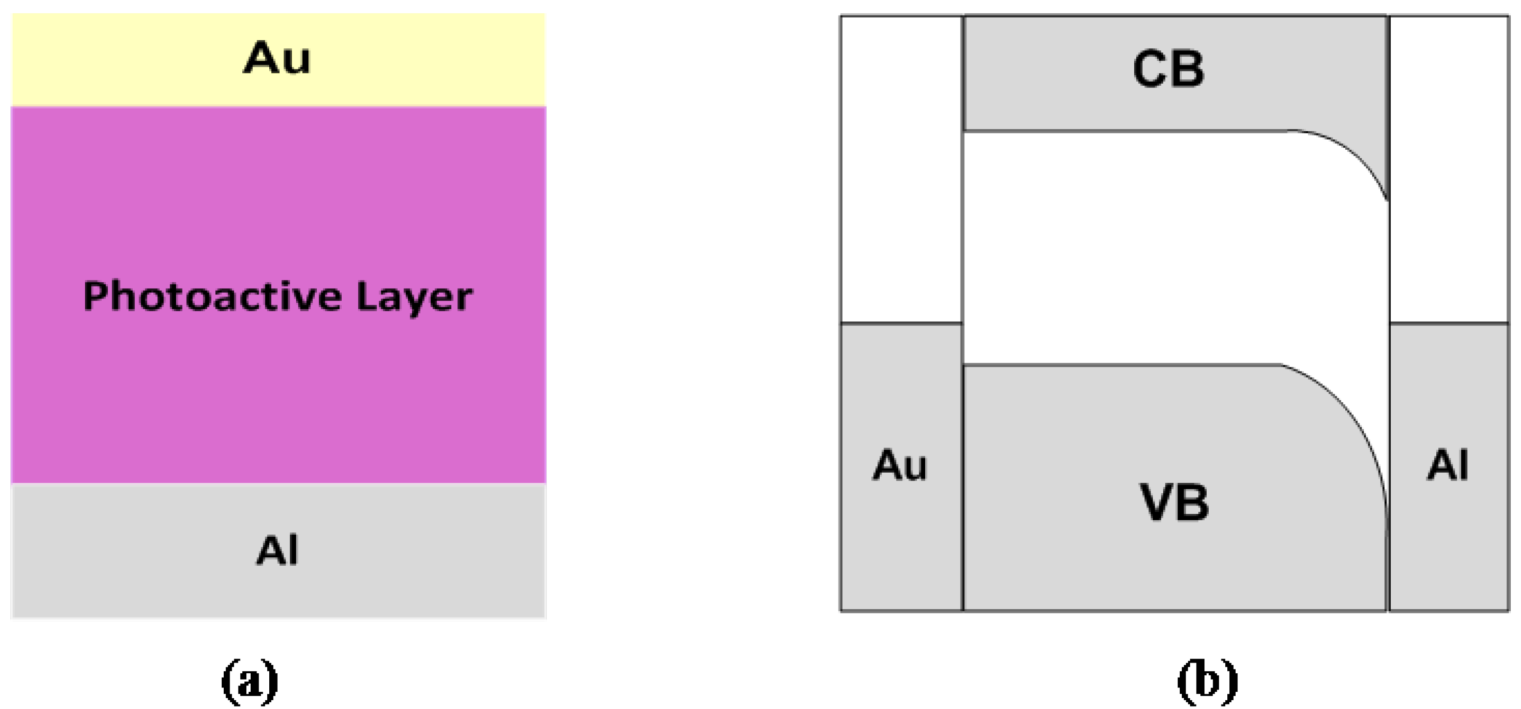
2.1.1. Single layer

The earliest OSCs were based upon an architecture that consists of a thermally evaporated organic molecular layer which is physically placed between two electrodes of different workfunctions. Commonly known as a sandwich cell, this arrangement facilitates the movement of charge carriers by the difference of workfunctions (Φ) in the anode and cathode. Rectification in single layer architectures is a close analogy to that in metal-insulator-metal (MIM) devices. A Schottky barrier is formed between the polymer and the lower workfunction electrode [12,13,14].
Figure 4. (a) Illustration of a single layer OSC and (b) Schottky junction at the high workfunction electrode under short circuit conditions.
Energies 03 01212 g004
If we take an example device with Au (higher Φ) and Al (lower Φ) as the electrodes we can observe that the energy bands bend to form a Schottky contact (due to alignment of the Fermi levels) (Figure 4). A small depletion region forms near the Al electrode. It is within this small depletion region that the excitons may diffuse to and dissociate, forming free charge carriers [15]. Unfortunately, the small diffusion length of the photogenerated excitons is problematic in this scenario as a large amount of recombination occurs which reduces PCE of the device.

2.1.2. Bilayer heterojunction

The introduction of the bilayer concept allows for higher efficiencies as it reduces the distance for the excitons to diffuse before dissociation and therefore significantly reduces charge carrier recombination. This idea is a very important step forward in OSC engineering—the new planar heterojunction interface. It consists of the combination of an electron donor (D) and an electron acceptor (A) material layer. The two layers are sandwiched between two electrodes, e.g., Au/D-A/Al. The electrodes are chosen so that their workfunction closely matches the highest occupied molecular orbital (HOMO) of donor and lowest unoccupied molecular orbital (LUMO) of acceptor [12].
The major advantage of this system is that the competing charge recombination is greatly reduced because the electron and holes travel solely in the appropriate polymer material phase upon exciton dissociation. Thus, the charge carriers are effectively separated within their corresponding donor or acceptor layer. The first breakthrough with this architecture is a device with a PCE of approximately 1% efficiency reported in 1986 by Tang (using a derivative of pthalocyanine as the donor layer material and a perylene derivative as the acceptor layer material) [2]. Other bilayer devices can be produced by sequential thermal deposition of materials [16,17,18,19] or by solution casting of one soluble material and evaporation of a second layer [20,21].

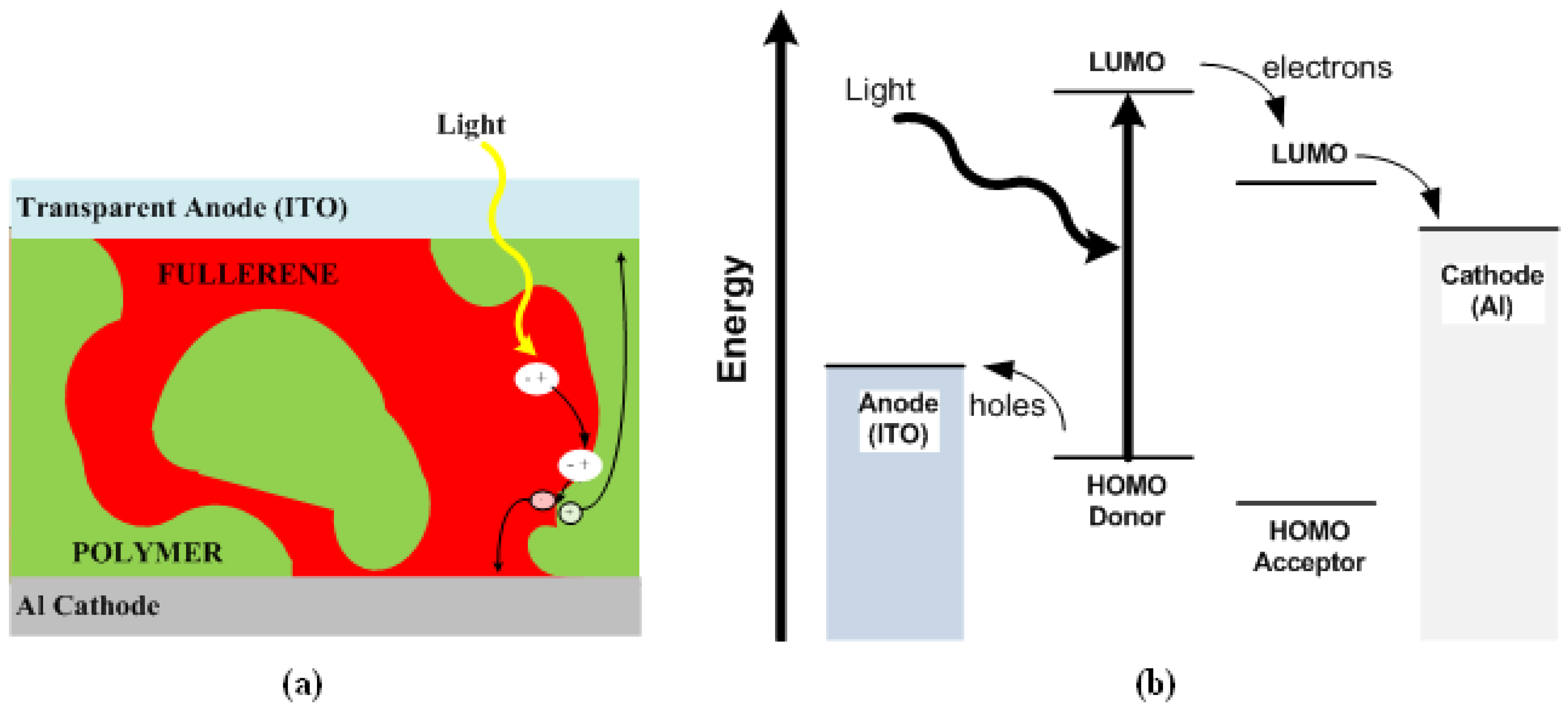
2.1.3. Bulk heterojunction (BHJ) 

This is the most common and efficient system currently employed in the active layer of an OSC. To date single or tandem OSC devices have been fabricated with the highest PCEs using this active layer architecture [8]. This is often called a blend structure where the donor (hole conducting) and the acceptor (electron conducting) materials do not have a planar interface. In a BHJ OSC, the active layer is a complex diffusive interface between the two materials in the form of a ‘bicontinuous interpenetrating network’ to maximize the available interface surface area (Figure 5). It has a nanoscale interpenetrating network with donor-acceptor phase separation in a length scale of 10–20 nm, which means each interface is within a distance lesser than the exciton diffusion length from the absorbing sites [22,23]. This interesting result shows that one can effectively maximize the exciton dissociation by using a BHJ active layer structure. Recent developments for organic donor and acceptor materials to reach higher efficiency OSCs showed great progress. Excellent reviews regarding this topic are suggested [8,24,25].
Figure 5. (a) Interfacial exciton dissociation in a BHJ OSC and (b) its band diagram.
Energies 03 01212 g005

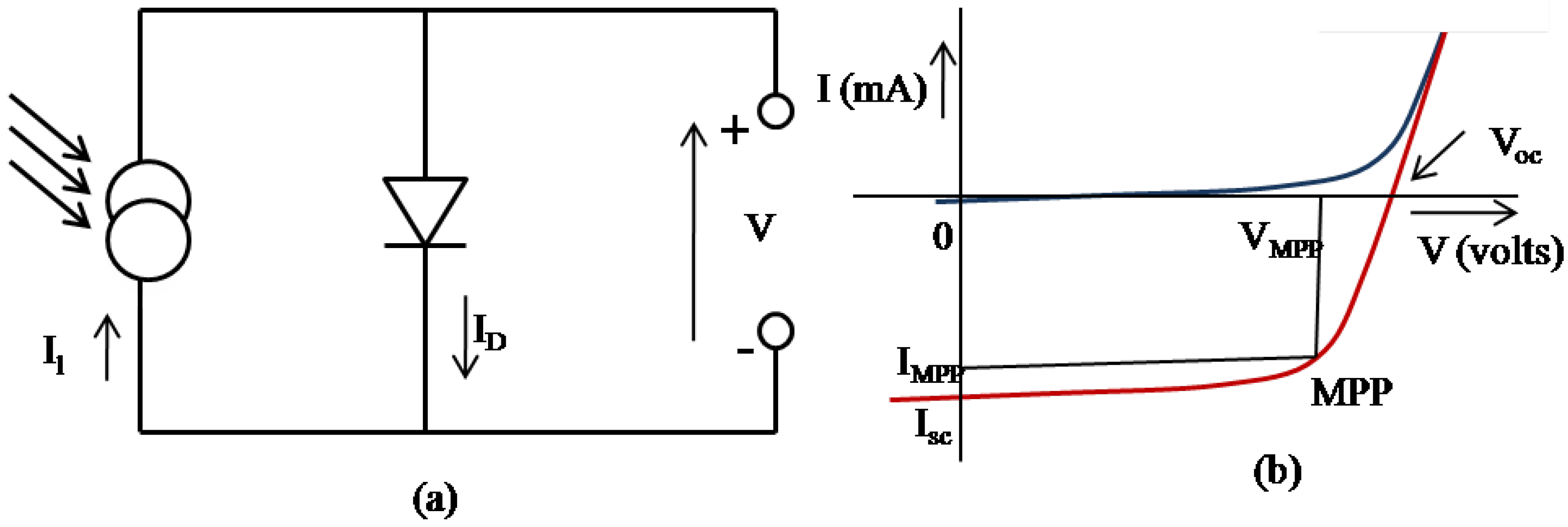
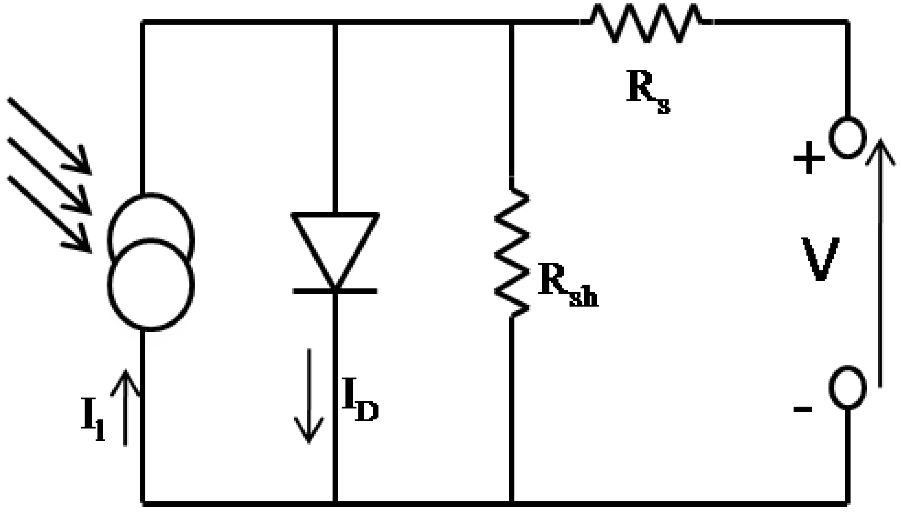
2.2. Critical parameters of an OSC

From equation (2) we see that the PCE of an OSC depends on the Voc, Isc and FF. For single layer OSCs, it has been demonstrated that the Voc follows the MIM model. It scales with the difference in workfunction between the cathode and anode [26,27]. This scaling of Voc is observed for bilayer OSCs as well but with an additional intensity dependent contribution from the active layer within the cell [28]. Voc for BHJ OSCs is directly related to the energy difference between the HOMO and LUMO levels of the donor and acceptor materials, respectively [29,30]. This is expected in cases where the workfunction of the anode matches the HOMO of the donor to form an ohmic contact and the cathode matches the LUMO of the acceptor forming a Schottky (non-ohmic) contact.
The advent of BHJ OSCs leads to an enhancement of Isc due to an increased interface area and hence, improved charge separation. The Isc still remains lower than those reported for inorganic devices. This is mainly due to poor absorption of sunlight by the photoactive materials used in OSCs and their low charge carrier mobilities leading to limited charge separation. The morphology of the active layer, solvents used and deposition methods also influence the Isc [26,31].
The dependence of FF on Rs and Rsh are graphically shown in Figure 3. The most commonly used transparent electrode, Indium Tin Oxide (ITO) has a relatively low conductivity that limits the FF on large area OSCs. A more conductive transparent material will minimize this problem. The shunt resistance can be maximized by making sure that there are no electrical shorts in the device.

2.3. Anodes

OSCs based on semiconducting polymer/fullerene BHJ penetrating networks of electron-donor and -acceptor materials have lead to conversion efficiencies >7.4% [32]. However these devices utilize ITO as the hole collecting layer (anode) and a low workfunction metal as the electron collecting layer (cathode). ITO is a good material in terms of transparency and conductivity but is brittle and readily cracks upon bending. This limitation on mechanical flexibility makes ITO substrates unsuitable for the manufacture of flexible OSCs. In addition to this, the scarcity of Indium and growing demand from the organic electronics industry, leads to increasing costs preventing large scale usage of ITO as an electrode for low-cost OSCs. Finding alternatives to ITO is a major area of research in the last five years. Some of the alternatives are doped metal oxides [33,34,35,36,37], organic polymers [38,39,40,41,42,43], metal grids [44,45,46,47], carbon nanotubes [48,49,50,51] and graphene [52,53].

2.3.1. Doped metal oxides

In the past, studies on transparent conductive oxides (TCOs) have been focused on ITO and Fluorine Tin Oxide (FTO). Recently, TCO films based on zinc oxide (ZnO) are receiving more attention because of their low cost, availability, low toxicity, high chemical and thermal stability. ZnO is a wide band-gap (3.3 eV), n-type semiconductor which in its pure form has a very high resistivity (108–109 Ω cm) [54]. This can be improved by doping with group III elements such as Al and Ga which have been reported as effective dopants for ZnO based films. OSCs using Ga doped ZnO (GZO) as an anode produced comparable results to those using ITO [33]. Schulze et al. did a comparative study of the properties of OSCs using ITO or Al doped zinc oxide (AZO) [34]. They reported that OSCs made with AZOs gave a similar Voc, Jsc and FF (~1 V, 8.14 mA/cm2 and 42.3%, respectively) to an OSC made with ITO. The workfunctions of AZOs depend on the doping level of the Al; however using AZOs with different doping levels in OSCs gave nearly the same Voc (~1 V). The authors attributed this to the presence of a doped transport (NPD or TNATA) layer on top of the anode which makes a quasi-ohmic contact between the AZO and the oligothiophene which is the donor material in the OSCs [55]. Bernede et al. inserted an ultrathin (0.5 nm) gold layer between the AZO anode and electron donor in the OSC (glass/ITO/Au/CuPc/C60/Alq3/Se-a). It resulted in a PCE of 1.4% which is ten times larger than the values achieved for OSCs without the gold layer—it gave a similar performance to OSCs using ITO/Au as the anode (as seen from the graph) [35]. The increase in PCE is attributed to changing the workfunction of AZO from 4.3 to 5.1 eV. The ultrathin gold layer reduces the barrier height at the interface of the anode and the HOMO of the donor, resulting in better hole extraction. Murdoch et al. reported that ozone treated AZO is an effective anode for CuPc-based OSCs [36]. Treatment with ozone decreases the resistivity of AZO by 40% from 2.3 × 10⁻³ to 1.4 × 10⁻³ Ω cm. OSCs fabricated with ozone treated AZO as an anode outperformed those without the treatment. The authors explained this through band alignment under Voc conditions employing quasi-Fermi-level splitting. Park et al. fabricated a multilayer anode Gallium doped zinc oxide (GZO)/Ag/GZO with low sheet resistance of 6 Ω/□ and a 87% optical transmittance by dual target DC sputtering at room temperature [37]. The low resistivity and anti-reflection properties of the Ag layer leads to the low sheet resistance and high transmittance observed in the GZO/Ag/GZO multilayer anode. The PCE of an OSC fabricated on the GZO/Ag/GZO (2.84%) is much higher than that of the OSC fabricated on GZO annealed at 500 °C (1.57%).

2.3.2. Organic polymers

PEDOT:PSS has emerged as a promising material to assist in band bending for the anode, enhancing the performance of the diodes. It is highly transparent in the visible range, has excellent thermal stability and is processable in aqueous solution. As a consequence, it has been widely used as a buffer layer for anodes in OSCs to improve hole extraction and prevent electrical shorting of devices by reducing pinhole defects. It has been observed that the conductivity of PEDOT:PSS films can be increased by more than an order of magnitude by the addition of poly-alcohols (alcohols with more than one OH group on each molecule) or high dielectric solvents such as dimethyl sulfoxide (DMSO). The mechanism for this observed conductivity enhancement have been debated. Ouyang et al. proposed that adding ethylene glycol (EG), meso-erythritol (1,2,3,4-tetrahydroxybutane), DMSO or 2-nitroethanol induces a conformational change in the PEDOT chain of the PEDOT:PSS film [38]. By using Raman spectroscopy they found that both coil and linear or expanded-coil conformations exist in untreated PEDOT:PSS films. The linear or expanded-coil conformation becomes dominant in high conductivity PEDOT:PSS films. This conformational change results in an increase in the intrachain and interchain charge carrier mobility and hence increases the conductivity. They reported an OSC of 1.5% PCE using high conductivity PEDOT:PSS (treated with meso-erythritol). Admassie et al. fabricated OSCs using vapor-phase polymerized PEDOT (VPP-PEDOT) and PEDOT:PSS/Sorbitol as anodes, showing an increase in PCE to 0.65% and 0.63% respectively compared to a PCE of 0.03% for devices with a PEDOT:PSS anode [39]. Na et al. compared the performances of OSCs fabricated on glass and flexible plastic substrates using PEDOT:PSS (Baytron PH500, H.C. Starck) by adding DMSO [40]. The performance of OSCs (PCE of 3.27% on glass and 2.8% on flexible plastic) is comparable to that of ITO OSCs fabricated on glass (3.66%) and flexible plastic (2.9%) substrates. They also demonstrated the superior mechanical robustness of the PEDOT:PSS/DMSO based cells. ITO based cells on flexible substrates failed after 75 bending cycles, while the efficiency of PEDOT:PSS/DMSO based cells on flexible substrates remained unchanged after 300 bending cycles. Furthermore, they investigated a recently developed PEDOT:PSS formulation, Clevios PH 510 (H.C. Starck), it’s conductivity can also be increased by adding DMSO [41]. In order to gain a better understanding of the nature of solvent-modified PEDOT:PSS films and the origin of its increased conductivity, they investigated changes in conductivity, morphology, surface composition, workfunction, and anisotropic conductivity in both parallel and perpendicular directions of DMSO treated PEDOT:PSS films. OSCs made by using modified (7% DMSO) PEDOT:PSS films gave a PCE (3.48%) which is comparable to OSCs made by using ITO on glass (3.89%). Ahlswede et al. added a mixture of DMSO, sorbitol and surfynol to PEDOT:PSS (Baytron PH500, H.C. Starck) and obtained a sheet resistance of 410 Ω/□ [42]. This was further decreased to 80 Ω/□ by coating an additional layer of PEDOT:PSS modified with DMSO and diethylene glycol (DEG). OSCs using this film gave an average PCE of 2.6%. Zhou et al. used a bilayer polymer anode on a polyethylene terephthalate (PET) substrate to construct flexible OSCs [43]. The bilayer consists of (i) PEDOT:PSS (Baytron PH500, H.C. Starck) modified with DMSO and a zonyl surfactant and (ii) PEDOT:PSS (Baytron P VP Al 4083, electroluminescent grade). OSCs using this bilayer anode gave a PCE of 2.23%, which is 80% of the PCE (2.78%) of OSCs made with ITO as anode. However, due to its low conductivity, using it as an anode for OSC fabrication gives very poor performance compared to ITO, and consequently as an electrode alternative, not a viable option.

2.3.3. Metal grids

A further decrease in the resistivity of PEDOT based anodes is achieved by applying a metal grid in between the substrate and the deposited film. Aernouts et al. used an Ag grid between the substrate and the PEDOT:PSS layer [44]. This device gave more than a threefold improvement in the short circuit current (1.8 mA) than the devices without the Ag grid (0.24 mA) because of the improved conductivity of PEDOT:PSS. Tvingstedt and Inganas observed that the overall transmission of the Ag grid is comparable to that of ITO in the visible region and superior to ITO in the near IR region of the spectrum [45]. The cells fabricated with the Ag grid between the substrate and DEG-PEDOT:PSS gave a higher PCE (1%) than the cells with ITO (0.83%) or with just DEG-PEDOT:PSS (0.63%). Kang et al. demonstrated that OSCs containing nanopatterned metal electrodes of optimum geometry showed essentially the same performance as devices made with high quality ITO electrodes [46]. The effect of workfunction of the nanopatterned electrodes on the device performance was analyzed showing lower workfunctions of the metal electrodes led to an increased FFs and PCEs by facilitating better charge transfer from the PEDOT:PSS layer. Nanopatterned Au and Ag gave PCEs of 1.96% and 2% respectively. Cu gave a PCE of 2.06% which is even higher than devices with conventional ITO (2%). Lee et al. reported a Jsc of 1.83 mA/cm2 using an Ag nanowire mesh which is 19% higher than that for devices with ITO (1.54 mA/cm2) [47]. This is attributed to the higher optical transmissivity of the Ag nanowire mesh, improved optical path length due to scattering of incident light by it, increased roughness of the donor-acceptor interface and possibly local enhancement of the optical intensity near the metal nanowires.

2.3.4. Carbon nanotubes

Another alternative to replace ITO are carbon nanotubes (CNTs) because of their superior conductivity. Pasquier et al. fabricated OSCs by using single wall carbon nanotubes (SWCNTs) as the anode [48]. They suggested the performance improvement of the OSC is due to the 3D connection of SWCNT with the photoactive composite (P3HT:PCBM). Rowell et al. used pure SWCNT films with a transmittance of 85% and sheet resistance of 200 Ω/□ to make an OSC on a flexible PET substrate and achieved a PCE of 2.5% which is comparable to the PCE of an OSC they made with ITO on glass (3%) [49]. The cells made with SWCNTs/PET were found to be more durable than cells made with ITO/PET upon bending. SWCNT devices can be folded to radii of ~5 mm without loss in PCE and radii of ~1 mm with a 20–25% loss while ITO/PET devices begin to fail at a radius of 1cm and completely fail at 5mm. Van de Lagemaats et al. fabricated an OSC with SWCNTs without using PEDOT:PSS and got a PCE of 0.47% while an OSC with PEDOT:PSS gave a PCE of 1.5% [50]. Tenent et al. reported methods to prepare SWCNT films with high transparency, low electrical resistivity and low surface roughness on large (6 inch × 6 inch) substrates by ultrasonic spraying [51]. A 40 nm thick SWCNT film with ~70% transparency (as seen from the graph) and resistivity 60 Ω/□ was used for fabricating OSCs and gave a PCE of 3.1% , comparable to that made with ITO (3.6% ). However, the downside of using nanotubes in any form of electronics is the problem of cost, until nanotubes are made at a cost significantly lower than that of graphite fibers, their likely use will be limited to laboratory devices.

2.3.5. Graphene

Reports detailing the possibility of using graphene to replace ITO have also been recently published. Wu et al. used graphene electrodes deposited on quartz substrates and obtained a PCE of 0.4%—almost half the PCE of the cells they made based on ITO (0.84%) [52]. The transmittance and sheet resistance values are between 85–95% and 100–500 Ω/□ for graphene films of thickness between 4 and 7 nm. Tung, et al. reported a competitive synthetic approach using a hybrid layer of carbon nanotubes and chemically converted graphene which is an inexpensive technology compatible with flexible substrates [53]. The sheet resistance (240 Ω/□) and optical transmission (86%) are comparable to that of ITO. OSCs made by this method gave a PCE of 0.85%. However, it is yet to be seen if this material is a viable alternative, as it is not so dramatically different from nanotubes or ITO, and will require significant investigation to determine its scientific and economic benefits as opposed to other carbon based materials.

2.4. Cathodes

The cathode is generally a lower workfunction metal deposited on top as the last layer of the OSC. The workfunction of the metal has direct influence on the extraction of electrons at the organic/metal interface. For optimum extraction it is important to match the workfunction of this electrode to the LUMO of the acceptor in the photoactive material. Therefore, the choice of metals for the cathode will depend on the photoactive material used. For BHJ OSCs, a metal with workfunction higher than the LUMO of the acceptor will form an interface barrier for electrons which reduces extraction; a metal with workfunction lower than the LUMO of the acceptor will reduce the Voc. Modification of the workfunction of metals to match the LUMO of the acceptor is an active area of research. A better understanding of how the critical parameters of an OSC are affected by the cathode materials is important to improve their performance. Ca or Mg are suitable candidates for cathodes but are easily oxidized. Al is commonly used as a cathode for OSCs. Mihailetchi et al. demonstrated that the Voc of the cells can be varied over more than 0.5 V by changing the workfunction of the cathode, the critical OSC parameters decrease with the increase of the workfunction [27,56]. Among LiF/Al, Ag, Au and Pd (Palladium) as cathodes for OC1C10-PPV:PCBM based OSCs, LiF/Al gave the best Voc and Jsc. This is because there is no energy barrier for electron extraction between the LiF/Al cathode and the PCBM (acceptor material). Ahlswede et al did a comparative study on the insertion of alkaline fluoride (LiF, NaF and KF) interlayers beneath the cathode [57]. The Jsc, Voc, FF and PCE showed a strong dependence on the type of alkaline fluoride (AF) and its thickness. All OSCs utilizing AFs showed an improvement in performance compared to OSCs without them. However, the optimal thickness for each AF OSC was different. The observed difference in the characteristics of LiF, NaF and KF interlayers could not be explained solely on the formation of a dipole layer at the interface. The authors suggested that it is more likely that the bulk of P3HT:PCBM is also changed due to enhanced dissociation and diffusion into the organic layer.
Zhang et al. reported the use of an organic buffer layer, poly(ethylene oxide) (PEO) instead of LiF. OSCs (ITO/PEDOT:PSS/APFO-5(LBPF3):PCBM/PEO/Al) with different thickness of PEO, estimated to be in the range 1–2 nm, showed significant increase in Voc (150–200 mV) [58]. All the OSCs with the PEO interlayer showed a higher PCE than those without. Improvement by more than 50% was attained in the best OSCs (PCE ~1.8%, from the graph provided). For the same thickness of the active layer, they reached a Voc of 0.82, 1.0 and 1.07 V for OSCs with Al, PEO/Al and LiF/Al respectively. I-V curves in the dark showed similar characteristics for OSCs with PEO and LiF, which suggest the similarity of the function of LiF and PEO. Reese et al. investigated the performance and stability of a range of OSCs (ITO/PEDOT:PSS/P3HT:PCBM/ PEO/cathode), by using Al, Ag, Mg:Ag/Ag, LiF/Al, Ca/Al and Ba/Al as cathodes [59]. All cathodes (with the exception of Ag) showed no greater degradation than 15% of PCE over a period of six weeks. The PCEs of all the OSCs with different cathodes were normalized with respect to a certified efficiency of 3.69% of Ca/Al cathode OSCs. Ba/Al and Ca/Al gave the best Voc (~600 mV) and the best PCEs, 0.96 ± 0.04% and 1.00 ± 0.04%, respectively. The FFs were also the best for these two electrodes, 60.6 ± 21% for Ca/Al and 62.2 ± 1.5% for Ba/Al. The LiF/Al cathode had a relatively smaller Voc (~580 mV), PCE (0.89 ± 0.03%) and FF (57.3 ± 1.2%). The authors attributed the difference in Voc between the low workfunction cathodes (Ca/Al, Ba/Al, LiF/Al, Mg:Ag/Ag) to the surface states that may be a result of different chemical interactions that occur at the cathode/active layer interface. However, Eo et al. did a comparative study of the metals Ca/Al, Mg/Al, Al, LiF/Al and Au/Al as cathodes in OSCs (glass/ITO/PEDOT:PSS/P3HT:PCBM/cathode) and gave a result which differs from the one stated above [60]. LiF/Al gave the best performance (PCE = 3.54%) the other cathodes ranged from 0.94–2.54%. This is consistent with the result stated earlier, there is no barrier energy for electron extraction between the LiF/Al and the PCBM based acceptor. OSCs with cathodes in the appropriate range between the HOMO of P3HT (5.1 eV) and the LUMO of PCBM (4.3 eV) showed superior performance than those outside of the appropriate range. It was concluded that electrode materials are one of the critical parameters that influence the performance of the OSCs.
The use of noble a metal for the cathode such as Au is desirable due to its resistance to oxidation. However, since the workfunction is higher than the LUMO of typical acceptors, it gives lower performing OSCs [27]. Li et al. reported a way to tune the workfunction of noble metals by adsorbing an air stable n-type dopant acridine orange base (AOB) thin film [61]. Ultraviolet Photoelectron Spectroscopy measurements showed that when a sub-monolayer of AOB was vapor-deposited on a gold substrate the workfunction was reduced from 5.2 eV to 3.5 eV. A more extensively deposited AOB layer gives a steady value of 3.3 eV at full coverage of the Au surface. Using AOB/Au as the cathode, OSCs (ITO/PEDOT:PSS/APFO3:PCBM/AOB/Au) fabricated showed a better Voc and PCE than OSCs with just Al. The PCE with AOB/Au cathode had a comparable PCE of ~2.25% (as seen from the graph) to OSCs with LiF/Al [62].

2.5. Inverted solar cells

Most common OSCs have the following structure: substrate/semitransparent cathode-hole collector/active layer/electron collector-anode. This device structure, where the anode is deposited as the last layer on top of the polymer blend will be referred to as the normal structure in this review. The low workfunction metal electrode in this architecture can be easily oxidized in air which is detrimental to the device performance. Therefore, encapsulation of the device is a necessary step to protect from oxidation. A way to circumvent this problem is to use the inverted structure, which has seen a lot of interest in the last five years. An inverted OSC has the structure: substrate/cathode contact/ electron collector/ active layer/ hole collector - anode depicted in Figure 6.
Figure 6. (a) Normal structure and (b) Inverted structure OSCs.
Energies 03 01212 g006
The low workfunction metal is in contact with the substrate while the high workfunction metal exposed to the air. The ITO-substrates which are used in the normal architecture can still be used in an inverted structure but the role is switched from collecting holes to electrons. The workfunction of ITO (4.5 to 4.7 eV) lies between the typical HOMO and LUMO of common active layers (such as P3HT:PCBM). This makes it possible for ITO to collect either holes or electrons depending mainly on the contact properties of the coating layer on top of the ITO surface. In the normal structure, it is coated with a high workfunction layer, usually PEDOT:PSS which collects holes. In the inverted structure, the workfunction of ITO is lowered by coating with a low workfunction material and it serves as the cathode.
Another advantage of the inverted structure is that it avoids the need for using PEDOT:PSS at the ITO surface. PEDOT:PSS is acidic in nature. Etching of the ITO can cause interface instability through indium diffusion into the active layer. Sahin et al. studied the stability of ITO/perylene diimide (or bathocuproine)/MEH:PPV:PCBM/copper pthalocyanine (CuPc)/Au cells in ambient conditions [63]. They demonstrated that such cells in ambient conditions are more stable than cells with Al as the top electrode in an inert argon environment because Au is more stable than Al. Hau et al. fabricated air stable inverted OSCs on ITO coated flexible plastic substrates by incorporating a thin layer of zinc oxide nanoparticles (ZnO NPs) which can be solution processed at room temperature [64]. They did a comparison of stability and performance of unencapsulated inverted OSCs fabricated using a high temperature (400 °C) sol-gel processed ZnO layer on ITO/glass, ZnO NPs on ITO/glass and ZnO NPs on ITO coated plastic substrates, to those of the normal devices using LiF/Al as the electrode on a glass substrate. Inverted OSCs made by high temperature sol-gel processed ZnO had an average PCE of ~3.5% while the normal OSCs averaged ~2.4%. The FFs of the two devices are similar but the Jsc and Voc of the inverted architecture are improved compared to that of the normal architecture. The better Jsc and Voc is due to the ZnO sol-gel layer which provides an additional n-type interface for electron transport. Inverted OSCs fabricated using ZnO NPs on ITO-coated glass gave an average PCE of ~3.6% which is very similar to that obtained from high temperature processed sol-gel OSCs. OSCs fabricated from ZnO NPs on ITO coated plastics gave a lower average PCE of ~3.3% due to the lower transparency (~80%) of the ITO-coated plastic in the region of 500–600 nm compared to the ITO-coated glass (~88%), thus reducing the photon flux from reaching the active layer (P3HT:PCBM). This is indicated by the lower average Jsc (9.8 mA/cm2) of plastic/ITO OSCs than that of glass/ITO OSCs Jsc (10.69 mA/cm2). The inverted devices using an Ag electrode are more stable than normal OSCs. They retained greater than 80% efficiency over 40 days while normal OSCs failed after 4 days. Li et al. made inverted OSCs using Titania (TiO2) as the electron collecting layer (ECL) and sulfonated poly(diphenylamine) (SPDPA) as the hole collecting layer (HCL) [65]. The inverted OSC (ITO/TiO2/P3HT:PCBM/SPDPA/Au/Ag) showed better performance (PCE = 3.91%) than normal OSCs made with PEDOT:PSS as the HCL. When stored without encapsulation in air, the inverted OSC maintained a PCE of 2.82% after 400 hours. From the graph provided, it could be seen that the PCE of the normal OSC declined rapidly (reduced by half after 30 hours) and failed completely after 300 hours. Zimmermann et al. fabricated long-term stable inverted OSCs which maintained 90% of their initial PCE after being exposed to 1500 hours of continuous illumination under a sulphur plasma lamp with a light intensity of ~1000 W/m2 at 50 °C corresponding to a light dose of approximately 1.5 years of sunlight [66]. The most efficient cells still had a PCE more than 2.5%.
An approach to improve the performance of inverted OSCs is by modifying the interface between the inorganic and organic layer with a self-assembled monolayer (SAM). Hau et al. demonstrated the improvement of inverted OSCs through appropriate SAM modification on the electron collecting layer [67]. The inverted OSCs (Glass/ITO/TiO2/SAM/P3HT:PCBM/PEDOT:PSS/Ag) using C60-SAM gave the best performance (3.8%) among OSCs using other SAMs (terthiophene, benzoic acid and lauric acid), i.e., 35% greater than OSCs without SAM modification at the TiO2 interface. The author attributed the better PCE to (a) reduction of contact resistance between the inorganic TiO2 layer and the active organic layer by passivation of surface trap states, (b) enhancement of the electronic coupling between the inorganic TiO2 and active organic layer to mediate better forward charge transfer and reduce back charge recombination at the interface and (c) changes in the upper layer growth mode and morphology, which all led to a reduction in series resistance and an increase in shunt resistance of the OSC. Furthermore, by replacing the ECL TiO2 with ZnO NP, the authors attained OSCs with a higher PCE of 4.9% [68]. The authors also proved that the SAM modification can be done in ambient environment. OSCs with SAM modification done in an ambient environment gave an average PCE of 4.45% which is almost as high as the average PCE (4.54%) of OSCs with SAM modification done in an inert environment.
Avoiding the use of ITO is favored because of the disadvantages discussed in the earlier sections. Efforts have been made and encouraging results have been obtained to replace ITO in the inverted structure by carefully choosing materials for electrodes with suitable workfunctions. Glatthaar et al. fabricated ITO free OSC using Al as the cathode [69]. The device (Glass/Al/Ti/P3HT:PCBM/ PEDOT:PSS/Au grid) has a FF of 53% which is typical for OSCs with P3HT:PCBM as the active layer. The author suggested that the low Jsc (4.6 mA/cm2) could be explained by the shadow loss due to the Au grid, a higher absorption loss in the PEDOT:PSS layer which is thicker than in normal devices and a lower light absorption due to a thin photoactive layer. Al-Ibrahim et al. did a comparison of normal and inverse P3HT:PCBM based OSC architectures [70]. Normal cells were fabricated using ITO as anode and Al as cathode. Inverted cells used Ti as the cathode and an ultrathin Au layer as the anode. The inverted OSCs showed comparable PCE (1.12%) to normal OSCs (1.54%).
Apart from an increase in stability, inverted structure OSCs give the possibility of developing a totally vacuum-free process for their fabrication, such as lamination processes or completely solution processed deposition on commercially available electrodes. Huang et al. fabricated metal free, semitransparent, flexible and self encapsulated OSCs with a PCE of 3% by a lamination process using modified PEDOT:PSS as an adhesive [71]. Nakamura et al. used thermal lamination for the introduction of top electrode of inverted OSCs and compared it with inverted OSCs where the top electrode is deposited by vacuum evaporation [72]. The OSCs (ITO/TiO2/PCBM:P3HT/Au) made using the lamination process gave a better PCE (2.6%) than those with a vacuum evaporated top electrode (1.6%). The authors suggested that the surface-segregated thin layer of P3HT may have been destroyed by vacuum evaporation, while the lamination process preserves the surface structure. Furthermore, the PCE of OSCs using the lamination process was increased to 3.3% upon insertion of a PEDOT:PSS layer between the Au electrode and the active layer. This was expected because a PEDOT:PSS layer improves hole collection. Zhou et al. used a solution process to fabricate transparent, inverted OSCs ITO/Polyethylene oxide/APFO3:PCBM/PEDOT:PSS(EL)/PEDOT:PSS (PH500) [73]. The PCE of the device is low (0.53%) and the authors suggested that it is due to less efficient absorption of the active layer and the high workfunction of the cathode.

3. Progress of Module Designs and Processing Technologies to Realize Large-Area OSCs

As the demand to deliver commercially viable OSCs is increasing, intensive research and investigation in the field has been directed to the materials design of the OSCs. However, limited effort has been directed towards the systematic optimization of other factors such as device area and electrode geometry. These factors also affect the performance of the OSCs, albeit to a smaller degree. It is clear that their influence cannot be neglected any longer as this field becomes more competitive.

3.1. Device area

The PCE of a solar cell depends on the FF, which is in turn based on the maximum power point of the cell and hence the series and shunt resistance of the cell [74]. As the series resistance of the cell is dependent on the area of the cell, an increase in the cell area causes slightly lower short-circuit current, lower fill factor, and lower PCE. Krebs et al. demonstrated that when the active area was reduced from 120 to 48 cm2 the PCE increased from 1.7 to 2.3% [75]. By reducing the active area the ohmic loss can be reduced, which in turn improves the efficiency. Al-Ibrahim et al. compared the performance of cells with different areas, 25 and 175 mm2 [76]. The range of FF and PCE of the smaller cells was 0.39–0.49 and 2.4–3.0%, respectively. The larger cells showed FF and PCEs of 0.34–0.37 and 1.48–1.70%, respectively. The author reasoned that the reduced currents in the 175 mm2 cells compared with the 25 mm2 devices were a consequence of the higher probability of pinholes and morphological inhomogeneities in the cells with the larger area, causing a smaller parallel resistance. The VOC remained constant irrespective of cell size.
Pandey et al. also studied the variation of electrical parameters as a function of OSC active area [77]. The series resistances obtained were 5.5, 16.0 and 34.6 Ω/cm2 for the cell sizes of 0.03, 0.28 and 0.78 cm2, respectively. They demonstrated that while VOC remains constant, the FF decreases causing the performance of the cell to diminish with increase in area. This result is in agreement with the observations reported [76]. The author suggested that the origin of losses in FF and ISC couldn’t be attributed to poor film quality of larger devices—it was due to the sheet resistance of the ITO. Choi et al. fabricated devices with two different areas 0.13 and 7 cm2 on ITO-glass. The devices show 1.2% and 0.41% PCEs, respectively. In small area devices organic semiconductor contribution to the resistive power loss is significantly more than that of ITO. However, power loss from the ITO is the only area-scaling parameter, making the limited sheet resistance of ITO a major limiting factor for large area cells [78]. Kang et al. described an approach to minimize the series bulk resistance by the lateral partitioning of the hole extraction layer by means of insulating walls [79]. Each divided active area acts like an isolated small cell so that the series resistance is reduced. When the hole collecting layer is partitioned into smaller sub-cells, a large area OSC device can be fabricated without negatively affecting the PCE. The 1 cm2 partitioned cell using Baytron PH-500 as the hole collecting layer showed about 40% improvement in the PCE over that of single cell (PCE increases from 2.75 to 4.32%).
It is essential to correctly measure the device area because it contributes to the calculated PCE. The top contact is evaporated through a shadow mask that determines the device area. The shadow effect occurs due to the misalignment of the top electrode with respect to the active layer. It is prominent when successive layers are evaporated from multiple sources causing a noticeable misalignment. Shrotriya et al. reported that the shadow effect is responsible for an error as high as 12% in current density values [80]. Only by positioning the mask in a very specific manner with respect to the deposition sources as outlined in [80] can reduce the shadow effect. To obtain accurate values of current density, the area of each device should be measured.

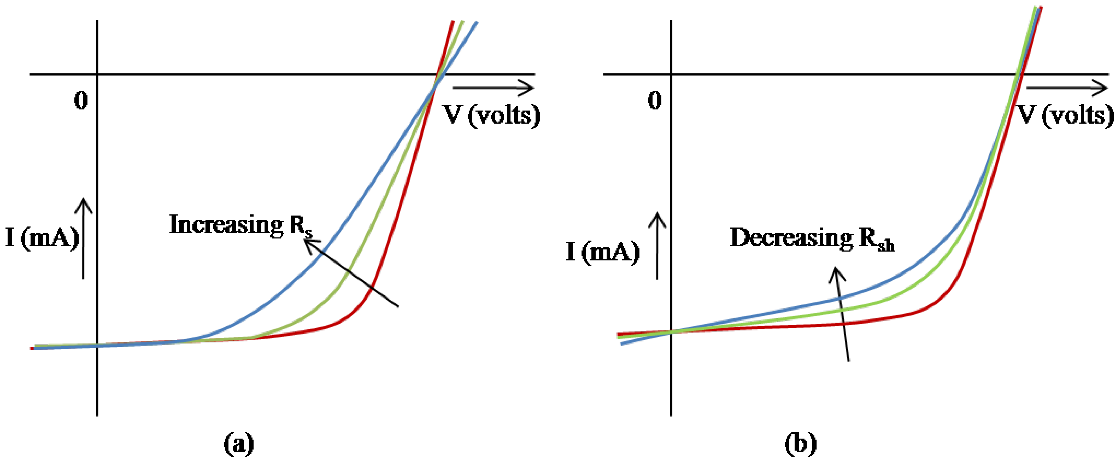
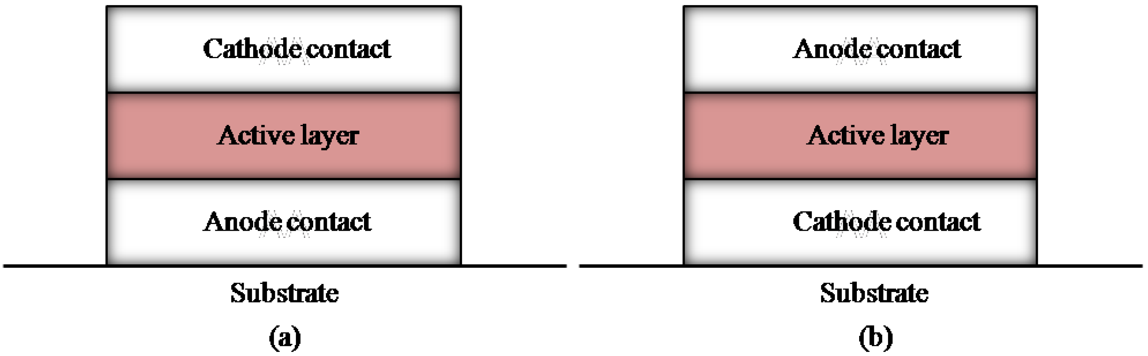
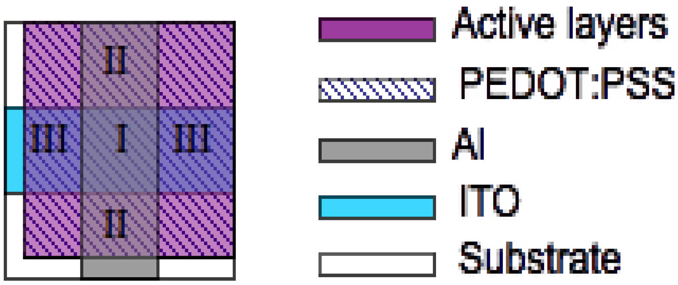
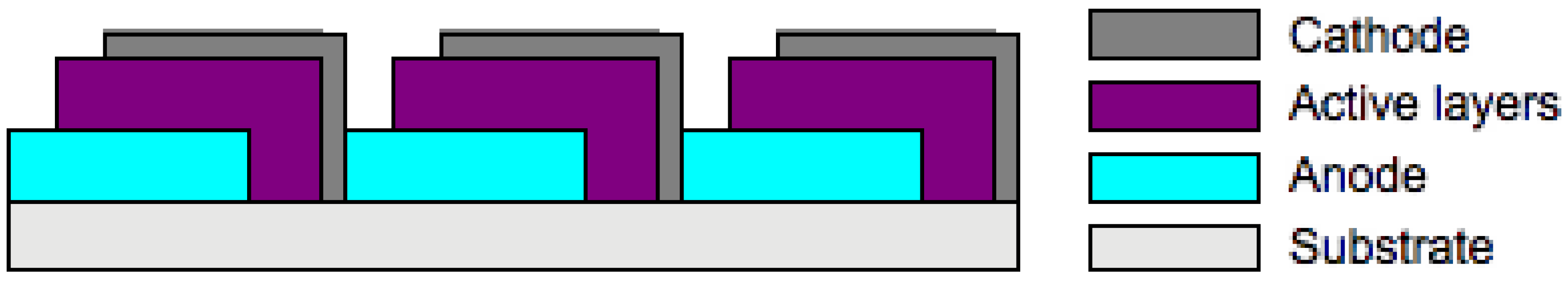
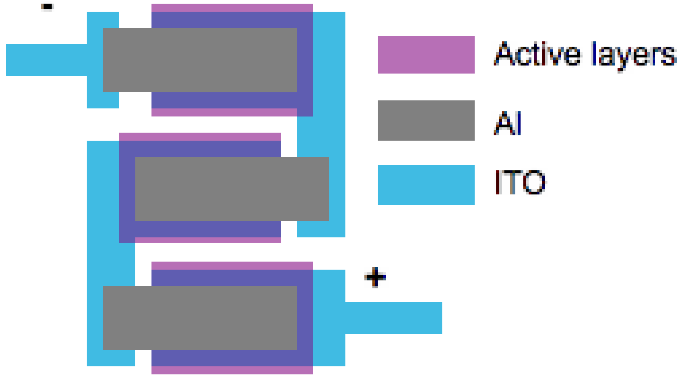
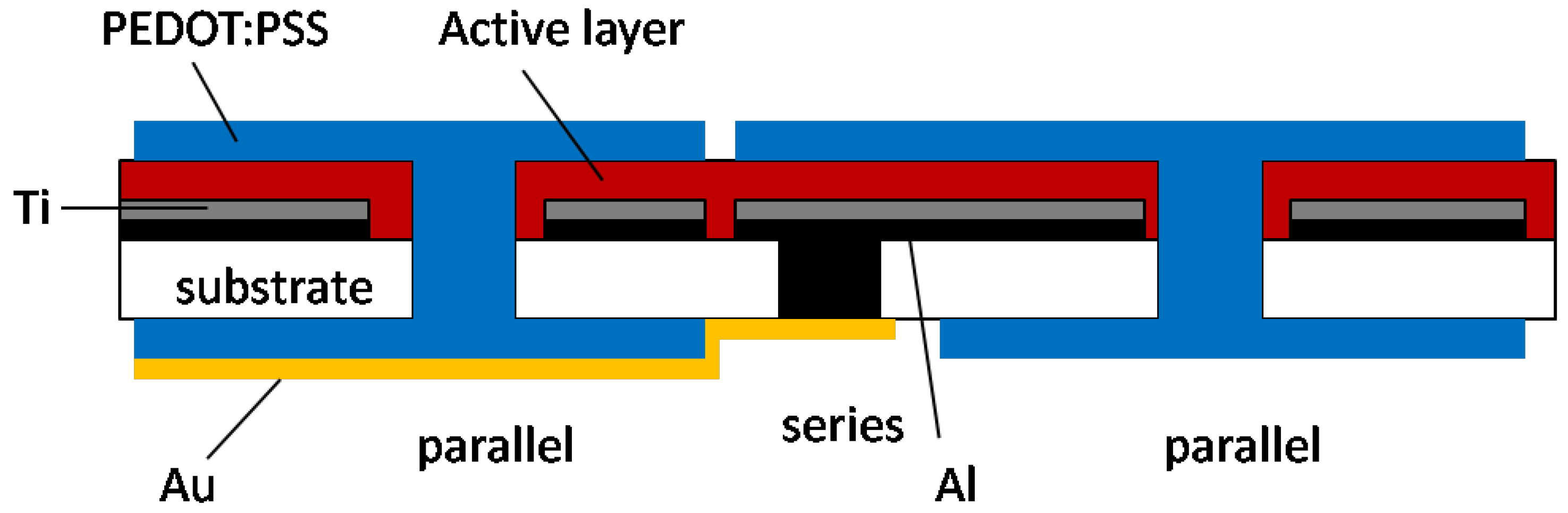
3.2. Effect of electrode geometry
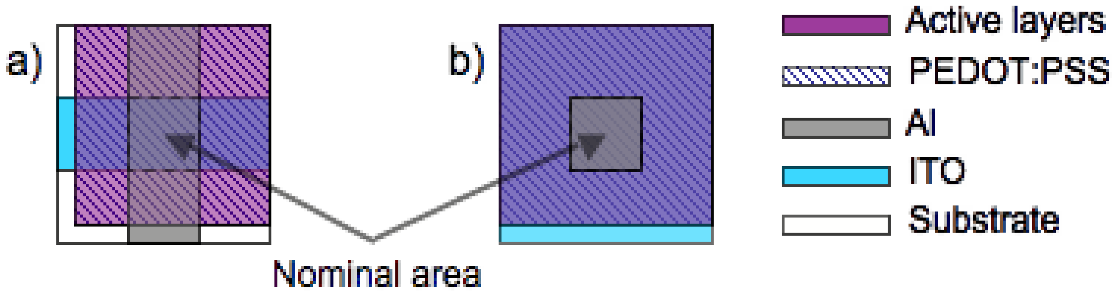
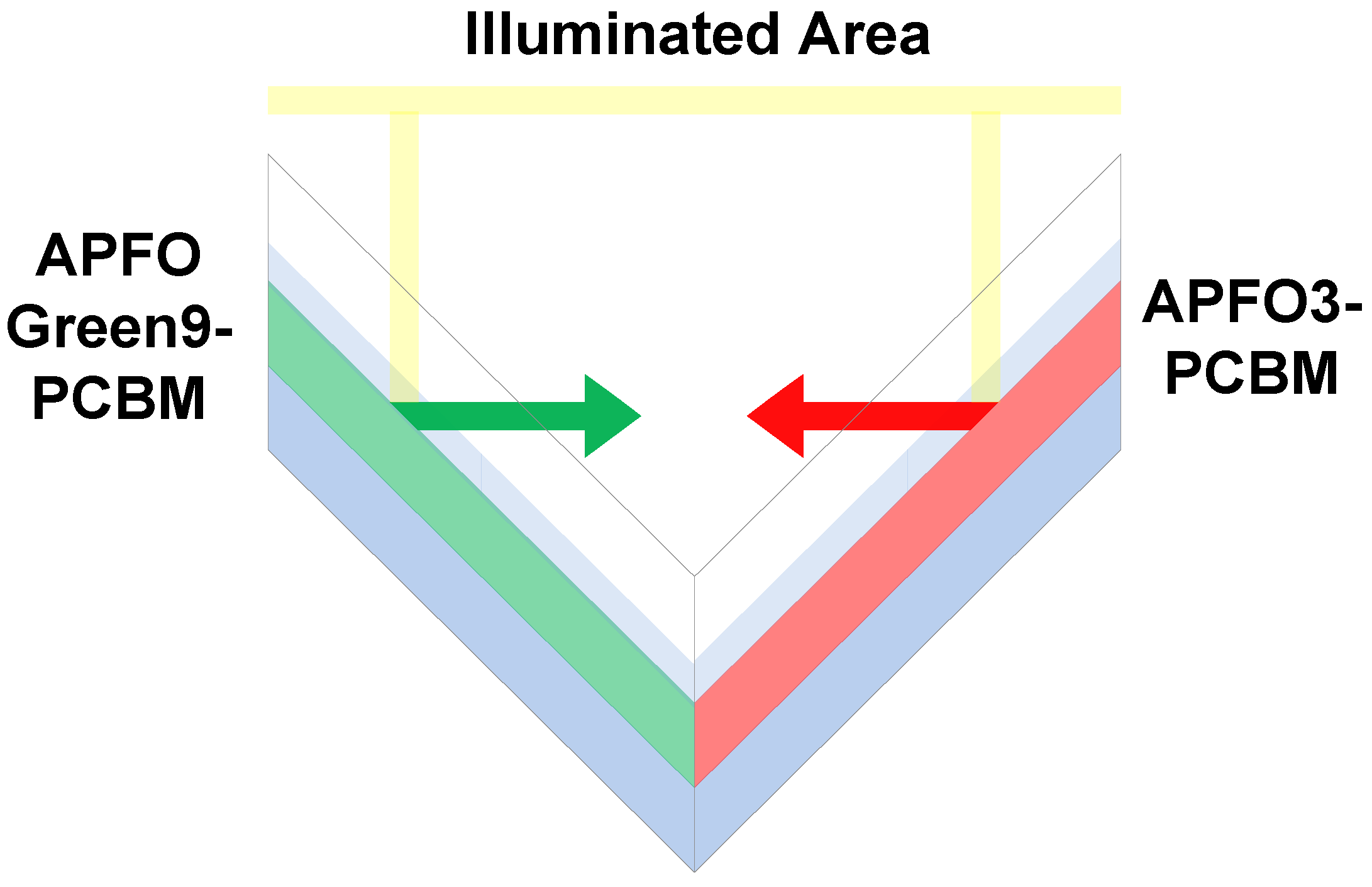
Cravino et al. and Kim et al. both reported how often overlooked factors such as device layout and electrode geometry can affect the evaluation of the PCE [81,82]. Two commonly used electrode geometries for OSCs fabricated at research laboratories are the crossbar and the island layout, as depicted in Figure 7. These layouts are routinely utilized for OSC research because deposition techniques such as spin-coating and doctor-blading are predominantly used.
The layout in Figure 7a is usually obtained when PEDOT:PSS and active layers are spin-coated onto patterned ITO and then the metal electrode is deposited perpendicular to the ITO, forming a crossbar layout. The ‘nominal’ area of each single photovoltaic element is defined as the overlapped region of the electrodes. The island layout (Figure 7b) is obtained when PEDOT:PSS and active layers are spin-coated onto unpatterned ITO. In this design, the metal electrode lies on top of a larger active layers/PEDOT:PSS/ITO substrate. Outside the nominal area, the active layer is only in contact with PEDOT:PSS/ITO.
Figure 7. (a) A crossbar layout and (b) An island layout.
Energies 03 01212 g007
In the crossbar layout, three distinct regions can be identified as shown in Figure 8. Region I is the "nominal" area. Region II is where Al/active layer/PEDOT:PSS overlaps without ITO. In region III the ITO/PEDOT:PSS/active layer overlaps without Al. Cravino et al. showed that a strong photovoltaic effect occurs in region II when it is illuminated. A photocurrent is generated and collected several millimeters away from the edge of region I. Kim et al. demonstrated that when the illuminated area is larger than the nominal area in the crossbar layout cell, excess photocurrent is generated from the photovoltaic regions outside the overlap area, where there is no ITO. They also show that the excess photocurrent is proportional to the conductivity of the PEDOT:PSS layer and increases with the illuminated area. This is due to the conductive PEDOT:PSS behaving as a substitute for ITO in region II. In region III only a small current contribution was observed because there was no cathode in this region. Based on the experimental results, the crossbar cells can be considered as two types of OSC connected in parallel: one is the OSC having ITO as the anode and the other is the OSC having PEDOT:PSS as the anode instead of ITO. If the beam size of the illuminated light is larger than the nominal area, devices with the crossbar layout will collect a non-negligible current from outside that area, resulting in a PCE that is higher than the actual value. To avoid this error inherent with the crossbar layout cell, the area of illumination should equal to that of the active electrode area of OSC. A more practical approach is to use the island layout cell, where no dependence of cell performance on beam size is observed. The design layout of the cells should be given due consideration and especially the crossbar layout of OSCs should be avoided. Precise patterning methods like ink-jet printing can eliminate these problems.
Figure 8. Schematic of an OSC with the crossbar layout. I: nominal area. II: substrate/ PEDOT:PSS/active layers/Al. III: substrate/ITO/PEDOT:PSS/active layer.
Energies 03 01212 g008
Lungenschmied et al. demonstrated that in large area OSCs, the dimension of the electrodes play an important part in avoiding unnecessary losses and improving the performance of the cell [83]. Using numerical calculations, they showed that the device efficiency reduces rapidly when the width of the solar cell increases. The efficiency varies from 0.5% for a broad stripe (length: 1 cm, width: 10 cm) to 3.1% for a narrow stripe (length: 10 cm, width: 1 cm). Depending on the ratio of the side lengths, efficiency was shown to vary by more than a factor of six. A cell design using electrodes in the form of narrow strips must have contacts on the long sides in order to minimize resistive losses. In such a design, the charge carriers travel only a minimum distance in the resistive ITO electrodes. Mushin et al. also studied various device geometries and their influence on the OSC parameters. They showed that incorporating short solar cell lengths and ITO bridges results in improved device performance [84].

3.3. Edge effects

In most OSCs where the active layer is fabricated using spin-coating [85,86] and doctor-blading [87,88] the active area covers most of the substrate and is not confined to the “nominal” area. The edge effect occurs when photocurrent is generated in those parts of the active layer, which is not in contact with the cathode. Cravino et al. observed this effect in the crossbar layout cell (Figure 7b) [81]. If the current density in the device is 10 mA/cm2 and the conductivity of PEDOT:PSS is 10–3 S/cm, photocurrent generated 10 μm away from the edges of the “nominal” device can still be collected, while causing a voltage drop of 10 mV. A photocurrent generated in regions II and III is transported respectively by PEDOT:PSS and by the active layer and will have losses due to their serial resistivity. This effect is negligible when the series resistance is low. In contrast, a large serial resistance causes a significant decrease in FF and VOC. Edge effects are more obvious at lower current densities and can be easily investigated by illuminating the region outside the nominal area. OSC devices with small areas are more susceptible to this effect. As edge effects will always be present to some extent in almost all OSC devices, it becomes significant as the area of the device reduces.
Research on OSCs has focused mainly on improving PCE for small laboratory cells. However, to upscale them from the research laboratories to mass production is equally important. Although PCEs around 4–5% [74,89] have been reported on very small active areas of 0.11–0.19 cm2, the performance of OSCs usually decreases as the area increases. To effectively cover large surfaces, individual OSCs should be connected together. A number of interconnected OSCs are needed to produce enough electrical power for most applications, as the PCE of a single OSC is usually low. There are two ways to connect the cells: in series or in parallel. Series connection is most frequently used to increase the output voltage of the module. When connected in parallel the currents of the individuals OSCs add up. In order to realize large-area OSCs with competitive PCEs, it is very important to compare various connection designs and study connection issues such as the losses occurring due to ineffective utilization of the aperture area and losses during the transport of the current.
In a typical OSC with moderate PCE, current densities ranging from 2 to 5 mA/cm2 are obtained. To get the maximum energy output from this range of current, electrodes with low sheet resistance are a critical requirement. Through an anode with typical sheet resistance of 50–100 Ω/□, a current density of 4 mA/cm2 can cause a minimum resistive voltage drop of 250 mV [90]. To avoid such resistive losses, a metal grid can be incorporated onto the transparent electrode to reduce the sheet resistance but this method adds extra processing steps. Another way to circumvent this problem would be to use very small individual cells. This would lower the sheet resistance of individual cells and allow efficient current collection. However, smaller cells cause more aperture area to be spent on interconnection and spacing, lowering the overall module efficiency. Dense packing of the cells should be utilized for maximal coverage of the aperture area. To achieve that, a method that allows precise patterning of organic and metal layers, without compromising device performance or adding significant cost should be used. Additional intra-module uniformity problems such as presence of shorted cells and/or cells with higher series resistance lower the attainable fill factor of the module. Ideally, the overall solar cell module performance should be a sum of the individual solar cell contributions. A module design is required to incorporate a suitable connection of individual cells having optimum area to keep the current losses at a minimum.

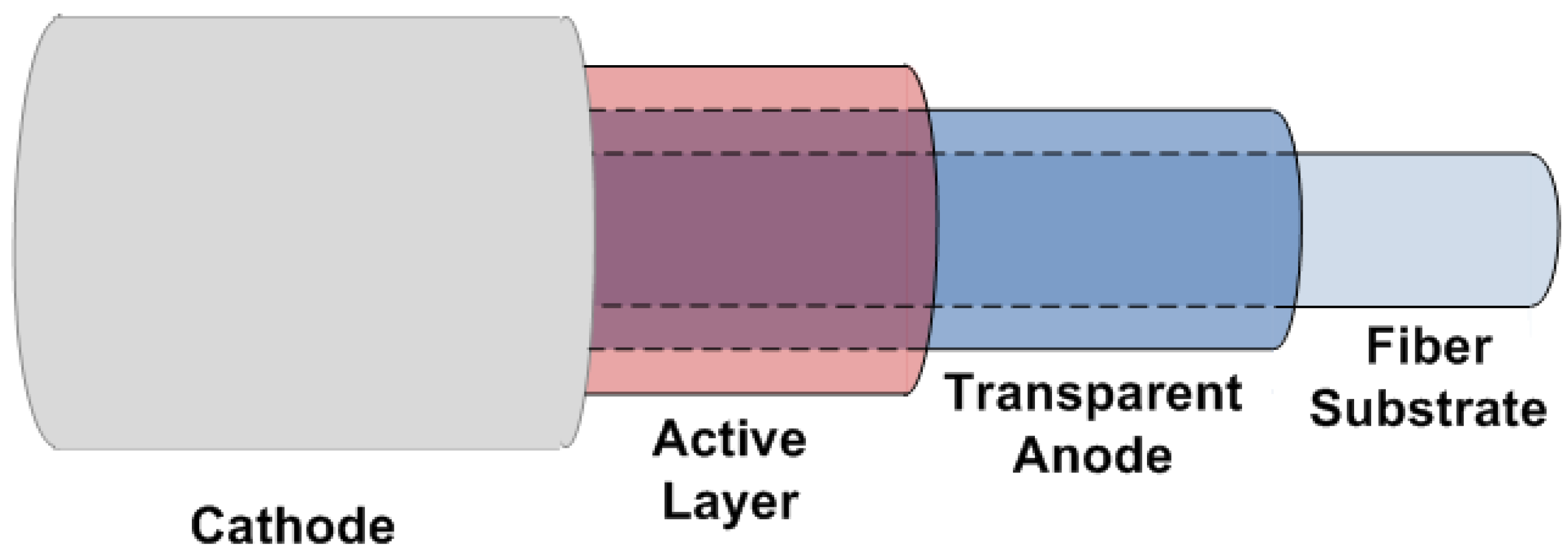
3.4. Large area solar cells

Solution processable polymers offer a major advantage for OSCs to be produced in high volume with low process cost. For OSCs prepared in research laboratories, the active layer has mostly been prepared by spin-coating [85,86] or doctor-blading [87,88]. However these methods are not suitable for large area, high volume production. Roll to roll compatible printing techniques such as screen-printing [90,91,92,93] and ink-jet printing [94,95] must be used for large area module production. A detailed processing knowledge for these methods is needed. Several different groups have started work in towards the realization of large-area mass produced OSCs and some of the results are summarized in Table 1.
The Krebs group is a major contributor to advance the manufacturing processes of large area OSCs. Their earlier works included the demonstration of the feasibility of industrial production of large area solar cells by silkscreen printing. The prototype devices consisted of three solar cells connected in series using the design in Figure 9. The PCEs of these devices are low (0.0046%) [91]. Later on, they experimented with a complex connection of the individual polymer solar cells to gain more information about issues regarding interconnections and power extraction [90]. They connected 13 cells in series to form a row then, seven such rows in parallel to give an OSC module of 0.1 m2 (Figure 10). The active area was 65% of the total area. The remaining area was used for interconnections between cells and for separations between rows. The overall module performance should ideally be a sum of the contribution of the individual solar cells. The VOC of 0.8 V of the 13 serially connected cells add up as predicted to give a module VOC of 10.5 V. In contrast, ISC and the efficiency were much lower than expected (0.1 μA/cm2 and 10−5%, respectively). The author suggests that contact problems, exposure to the atmosphere and electron damage due to radiation during e-beam evaporation of the aluminum electrodes may be possible reasons for this behavior.
Table 1. Parameters and performance of OSC modules mentioned in this review.
Device structureaConnectionAreab (cm2)JSC
(μA/cm2)
ISC
(mA)
VOC (V)FF (%)η (%)Reference
ITO-PET/MEH-PPV/C60/Al3 Sd~30e20---0.73490.0046 [91]
ITO-PET/MEH-PPV/Al13S Χ 7Pg6550.1---10.5130.00001f,c [90]
ITO-PET/MEH-PPV/C60/Al13S Χ 7Pg6553.5---3.6190.0002 f,c [90]
ITO-Glass/PEDOT:PSS/P3HT:PC70BM/Al4 Sd1.04---1.42.48441.7c [96]
ITO-Glass/PEDOT:PSS/P3HT:PCBM/Al2 Sd17.1---56.51.14421.5c [83]
ITO-Glass/PEDOT:PSS/P3HT:PCBM /Al3 Sd11.3---27.21.66391.5c [83]
Flexible Foil/ITO/PEDOT:PSS/P3HT:PCBM /Al3 Sd11.3---13.91.38290.5c [83]
ITO-Glass/ PEDOT:PSS/ P3HT:PCBM/Al22 Sd46.2---16.5612.45432c [97]
ITO-PET/ZnO/P3HT:PCBM/PEDOT:PSS/Ag8 Sd120---159.973.76351.78c [75]
ITO-PET/ZnO/P3HT-PCBM/PEDOT:PSS/Ag8 Sd120---603.6442.08 g,c [75]
ITO-PET/ZnO/P3HT-PCBM/PEDOT:PSS/Ag8 Sd4.8---6.873.62442.33c [75]
ITO-PET/ZnO/P3CT:ZnO/PEDOT:PSS/Ag8 Sd120---6.822.99290.05c [98]
ITO-PET/ ZnO /P3CT:ZnO/PEDOT:PSS/Ag5 Si75---0.1316j0.013c [92]
ITO-Glass/ HTL/P3HT: PCBM/Ca-Al54 Sd108---16.9129.35513.4c [99]
ITO-Glass/PEDOT:PSS/P3HT:PCBM/Al3Sd16.29000---1.94523.0c [100]
The measurement conditions are 1000 W/m2, AM1.5G unless stated otherwise. The values are for modules unless stated otherwise. a ITO = Indium tin oxide; PET = polyethylene terephthalate; MEH-PPV = poly[2-methoxy-5-(2'-ethyl-hexyloxy)-1,4-phenylene vinylene]; PEDOT:PSS = poly(3,4-ethylenedioxythiophene):poly(styrenesulfonate); P3HT = regioregular poly(3-hexylthiophene); PCBM = phenyl-C61-butyric acid methyl ester; ZnO = Zinc Oxide; HTL = hole transport layer, Plexcore® OC; PC70BM = phenyl-C71-butyric acid methyl ester; b Total active area; c Active area efficiency; d S = cells in series; e Adapted from Figure 2 using the scale bar provided; f 13 cells in series to form a row, then 7 such rows in parallel; g Incident light 950 Wm−2; h Incident light 393 W/m2 ; i 5 circular cells in series; j As mentioned in Figure 9 in [92].
Figure 9. Serial connection of three cells (adapted from [91]).
Energies 03 01212 g009
Figure 10. Serial connection of organic solar cells.
Energies 03 01212 g010
Yoo et al. fabricated an OSC module with a scalable voltage output using P3HT:PC70BM [96]. It was shown that the VOC scaled linearly: if N is the number of OSC connected in series, VOC (N) = N × 0.621 V, giving a VOC of 2.48 V for four serially connected cells. The efficiency decreased from 2.2% for an individual cell to 1.7% for four serially connected cells (AM1.5G, 850 W/m2). This was attributed to the cell-to-cell variation in the series resistance.
Lungenscmied et al. demonstrated interconnected organic solar cells on glass substrates as well as on flexible ultra high barrier foils [83]. The total active area of the modules was 11.3 cm2 and 17.2 cm2 for three and two cells connected in series, respectively. The highest PCE was 1.5% for glass and 0.5% for a flexible substrate when three cells were connected. The PCEs were lower than that predicted theoretically because of the high degree of inhomogeneity and defects which occur on large-area substrates. This was more evident as the cells were not manufactured in a clean room environment. The series connection was done manually, so it doesn’t represent a viable procedure on an industrial scale. For scaled up production, different techniques such as selective laser scribing would be required.
Niggemann et al. developed a module which consisted of two monolithically interconnected segments consisting of 11 cells each, yielding 22 interconnected cells [97]. The ITO was patterned either by photolithography or by laser scribing. The PEDOT:PSS was patterned by microcontact printing a self-assembling monolayer. The patterning of the photoactive layer was done using mechanical scribing. A PCE of 2% was obtained for an active area of 46.2 cm2 (1000 W/m2, AM1.5G). Under indoor illumination of 500 to 1000 lux, an operating voltage between 4–5 V was realized. The absence of the electrical shunt defects, despite the relatively large module size of 64 cm2 is promising for future large scale production.
Mushin et al. prepared OSC modules on glass substrates. The device area of each cell was 5.4 cm2 and the average PCE was 3%. The module efficiency was 1.9% when three such cells were connected in series. They stressed the importance of highly homogeneous active layer thickness to obtain a large average photocurrent density [100].
The Krebs group worked with modules comprising of two, three and eight serially connected cells [75]. By using an inverted geometry (substrate/ITO/ZnO/P3HT:PCBM/ PEDOT:PSS/silver), they developed a fully roll to roll solution process to manufacture OSCs. When the active area is reduced from 120 to 48 cm2 for the 8 serially connected cells, the PCE increases from 1.7 to 2.3%. They concluded that the performance was limited by carrier extraction. By reducing the active area, the ohmic loss can be reduced, which in turn improves the PCE. In another work by the Krebs group, P3CT:ZnO was used as an active layer [98]. Although the PCE of the OSC was low at 0.05%, P3CT:ZnO devices can be operated in the ambient atmosphere with good operational stability under illumination (1000 W/m2, AM1.5G, 72 ° 2 °C, 35 ° 5% relative humidity) for 100 h with only 20% loss in PCE with respect to initial performance [101]. This enabled mass production of modules using all solution processing without vacuum steps. They also explored a module design with circular geometry, in which five concentric rings were connected in series [92]. The typical ISC and VOC of the modules were around 0.1 mA and 3 V, respectively. The best PCE obtained was 0.013% for the 75 cm2 active area. This module used P3CT:ZnO as an active layer, which made it resistant towards both oxygen and water.
Tipnis et al. fabricated a very large laboratory scale OSC module having a total area of 233 cm2 [99]. Two configurations were explored, one in which 54 individual cells were connected in series and another in which nine cells were connected in series to form a row, and six such rows in parallel. The OSC was produced using P3HT:PCBM as the active layer over a hole transport layer—Plexcore® OC. The module (area) efficiency was 1.1% while the active area PCE was 3.4% (total area of the module: 233 cm2, active area: 108 cm2).
The high series resistance of the ITO is an impediment for reaching high module efficiency because it causes ohmic losses hampering the cell performance. This can be demonstrated by taking apart the cells from a module and reconnecting them again through external wiring. The latter arrangement gave a better performance than the module. Zimmerman et al. demonstrated a ‘wrap through concept’ as an alternative idea for large area ITO-free polymer cells (Figure 11) [102]. The current is collected on small areas to minimize the ohmic losses. The current carrying through PEDOT:PSS anode is then led through vias in the device to the back-side of the substrate, which is coated with a thin metal layer on top of the PEDOT:PSS layer to form a scalable parallel circuitry. The presence of the low resistance metal layer on the polymer anode reduces the ohmic losses. It increases the module efficiencies to 89% of the elementary cell in comparison to 83% for ITO on glass and 75% for ITO on polymer substrate. Devices with active areas of 2–4 cm2 have been manufactured with PCE values 1.8–2%. A series connection can also be achieved monolithically on the substrate by connecting the cathode and the metallic back contact through additional vias in the substrate (Figure 11). The first device with this circuitry was composed of two wrap through cell segments showing a PCE of 1.1%. Each segment (2 cm2) was connected in series monolithically.
Figure 11. Monolithic serial circuitry in combination with the parallel circuitry based on the wrap through concept (adapted from [102]).
Energies 03 01212 g011
Series interconnection of single cells in a module is an effective way of achieving high module voltages. One of the disadvantages of this circuitry is the occurrence of a failure mechanism, namely the ‘shading’ failure. When an illuminated OSC is partially shaded, the shaded cells behave as a load resistance for the rest of the circuit. In such a case, the electrical power generated by the illuminated part of the module will drive the cell in reverse bias. This can cause severe consequences because electrical power generated may heat up the shaded cells resulting in cell failure. Steim et al. demonstrated the use of organic by-pass diodes to reduce the adverse effect of shading on the module power output [103]. A module of nine serially connected cells with the last module cell shaded was investigated. The power loss of 99% was significantly reduced to ~30% by using an organic bypass diode interconnected anti-parallel to the module OSCs. An unilluminated OSC in reverse operation was used as a bypass diode making it easier to integrate it into a module.

4. Optimization of OSC Performance through Device Engineering and New Architectures

Research groups aiming to improve the PCE of OSCs have been primarily focused on modifying parameters pertaining to the flat panel architecture conceived for inorganic photovoltaics. It has become clear that the traditional flat panel architecture is not well suited to OSCs due to the limitations imposed by the available polymers used as active layer materials. Loss due to reflection by the various device layers is less of a problem for organics where reflection at an air-glass is less than 4%. This compares well to that of inorganics such as silicon (reflection at an air-silicon interface is approximately 30%) [104]. However, the poor mobilities of active layer composites (ranging between ~10−5 to 1 cm2/Vs) [105] in combination with short exciton diffusion lengths (10–20 nm) [106], require the active layer to be kept very thin (20–250 nm) [107] compared to that of silicon cells which are of the order of several hundred microns [104]. This difference is very significant when looking at the amount of light absorbed in the active layer which is exponentially dependent upon the layer thickness most basically described by the Beer-Lambert law for absorption. The use of very thin films in the active layer results in a substantial amount of incident light being transmitted. The initial coupling of light into the device at normal incidence is not subject to much reflection losses. However, all light that is not absorbed by the active layer upon back-reflection from the nontransparent electrode escapes the device reducing the possible attainable PCE. To date, there a very few materials which can be combined to form composites for the active layer which give a high PCE [108]. The composites used to make even the most efficient devices (P3HT:PCBM) have a very small absorption range which poorly match the solar spectrum. The search for possible low-bandgap polymers [109,110,111,112,113] capable of absorbing more of the incident light is ongoing but this will not solve the problem of light lost due to the limitations of the flat panel architecture.

4.1. Modification and optimization of flat panel architectures

The modification of flat panel architectures in order to realize their maximum potential has seen a number of different approaches with varying levels of success. There is a large body of work describing various optical modeling techniques. Their main aim is to try and optimize the behavior of the light in the device by means of adjusting the layer thicknesses so that there is a better spatial intensity distribution of the electromagnetic field within the device—ideally having the majority of the energy within the active layer. Without considering the electrical properties of the materials however would result in a very thick active layer which would indeed lead to a very high level of absorption but also very poor PCE due to the aforementioned short exciton diffusion lengths. The solution to this is the use of optical modeling (such as the transfer matrix method, finite element method or rigorous coupled wave analysis) integrated with electrical models which allows for the optimization of actual device performance which may be viewed in detail in the following reviews [114,115,116]. These electro-optical models are also used to investigate significant interference effects which play a major role in flat panels. They focus on the optimization of the layer thicknesses within certain limits to maximize efficiency under the restrictions imposed by electrical properties of the materials.
Optical spacers such as TiOx [117,118] and ZnO [119] have been utilized to further tailor the distribution of light intensity within the device attempting to ensure there is a local optical maximum at the donor – acceptor interface. However, Andersson et al. have started the debate on whether optical spacers have any tangible positive effect at all and conclude that in the case where there is a suboptimal active layer thickness an improvement may be seen with the addition of an optical spacer [120]. They deem that the inclusion of an optical spacer in the flat panel architecture does not merit the added complexity in fabrication. This opinion may remain true until the application of optical spacers in tandem cells is examined.
Tandem solar cells are flat panel devices which have a back cell and a front cell interconnected (most often serially) to form a so called ‘double heterostructure’ (where two donor materials are used) [121,122]. These tandem cells introduce a method of absorbing a larger amount of energy from the incident solar light on the device. The concept of these slightly modified flat panel devices is to absorb more of the solar spectrum by means of the additional active layer which complements the absorption of the first. A further progression to this idea, multi-junction cells having more than two active layers and those being a hybrid of organic and inorganic materials have also being conceived. Hadipour et al. gives an in depth discussion on the fabrication and performance of a range of tandem and multi-junction devices [123].
The introduction of more efficient light collection or concentrator elements has being carried out in order to reduce the loss of light thus increasing external quantum efficiency (EQE)—a measure of current output as a function of incident photons. Anti-reflective, dielectric coatings are more suitable for inorganic devices which have for example an air-silicon interface which is considered quite reflective. It stands to reason that by means of using an anti-reflection coating it allows more light to enter the device but in real terms may allow more to leave unabsorbed [107]. It is counter-productive; it improves initial coupling of light into the cell but it also improves the rate at which light can escape the cell. Another means must be employed which will have either a method of reducing initial light reflection from the glass or plastic substrate and also simultaneously trap the increased amount of light that has entered the device.
Modification of the standard flat panel substrate architecture has been investigated by the incorporation of concentrating elements such as solar collectors [124] and micro lens structures [125]. Nano structures including patterned and embossed gratings [126,127], diffraction gratings and buried nano-electrodes [128] have also being proposed. Light confinement and even better light trapping methods are seen as a solution to enhance the EQE. Zilio et al. have developed a new kind of light trapping element fabricated on a glass or plastic substrate which comprises an array of small apertures in a reflective silver film (mirror) on one side and an array of micro lenses focusing light onto these apertures on the other (Figure 12) [129]. The light trapping efficiency is strongly related to the size of the mirror openings which when optimized is a trade-off between allowing enough light through the apertures without hampering the reflection coefficients. They report that by using this light trapping structure it may be possible to increase the PCE by approximately 25% relative to the standard flat panel substrate [125]. Actual efficiency values were not reported by the authors.
Figure 12. Schematic of light trapping device proposed by Zilio et al. (adapted from [129]).
Energies 03 01212 g012
Luminescent concentrators can be used to ‘convert’ light to a more desirable wavelength [130]. Currie et al. describe the use of short wavelength and longer wavelength dyes which are deposited onto large area high refractive index glass substrates which act as light collectors (Figure 13). The dyes absorb incident photons and reemit them by means of fluorescence or phosphorescence at a lower energy into a waveguide. Around 80% of the reemitted photons are trapped in the waveguide by means of total internal reflection and are subsequently channeled to solar cells at the periphery of the collector [131]. This concept shows great promise for increasing the efficiency of organic solar cells as well as having interesting applications for windows that can generate electricity.
Figure 13. Schematic of light behavior in the luminescent solar concentrator device utilizing two dye coated substrates (adapted from [130]).
Energies 03 01212 g013

4.2. Progression to new architectures

In order to address the problems seen with flat panel devices, it is clear that rethinking how organic solar cells are fabricated, using architectural changes by means of new designs not based upon simple flat panels has yielded interesting results. The first deviation from the standard flat panel is what can be described as a new kind of folded tandem solar cell or ‘v-geometry’ (Figure 14) [132,133,134,135]. This new v-geometry ‘flat panel’ tandem cell allows more freedom to accommodate a range of materials without the added complexities and restrictions imposed by the layered structures seen in the standard tandem and multi-junction cells discussed previously. The main result of this geometry is by means of spectral broadening and the confinement of light PCE is increased. Tvingstedt et al. report that this simple geometrical modification enhances the optical absorption especially at higher degrees of folding giving increased photocurrent generation leading to relative increases in PCE by a factor of 1.8 ± 0.3 (from 2% up to 3.7% upon changing the angle from 0 to 70°). Altering the angle between the two cells controls the confinement of the incident light by taking advantage of multiple reflections within the structure, thus increasing the effective pathlength of the light within the active layer.
Figure 14. Illustration of the v-geometry OSC (adapted from [133]).
Energies 03 01212 g014
An intrinsic light trapping design, the optical fiber or the cascade (micro-concentrator) photovoltaic cell is a unique concept which is based upon an architecture that is light trapping due to the very nature of an optical fiber (Figure 15) [136,137,138]. This kind of architecture makes use of a waveguide as the substrate for the solar cell into which the incident light is coupled. Light is essentially trapped and travels within the device along the fiber axis making multiple passes through the active layer thus significantly increasing the EQE. The cylindrical geometry of a fiber makes it useful in a number of ways—if the cell is fabricated so that light enters from the side walls it may then efficiently couple diffuse light (light over a range of incident angles) into the active layer, reducing the problems seen with conventional cells due to partial shading and possibly removing the need to incorporate solar tracking [138].
Figure 15. Diagram of optical fiber solar cell (adapted from [136]).
Energies 03 01212 g015
The methods discussed for improving flat panel devices are indeed a step in the right direction for improving PCE. Persisting in using the flat panel architecture designed originally for inorganics may not be the best approach to achieve efficiencies of 10% and above which can compete with fossil fuels. New light-trapping geometries need to be conceived. This could be realized by building upon the concepts of the folded v-geometry and fiber-cells. A combination of using novel geometries and incorporating some of the concepts proposed for improving flat panel devices may lead the way for the long awaited high PCE devices.

5. Conclusions

In this review, recent developments in the field of materials design and architecture of organic solar cells are discussed. Innovations focused on three issues, power conversion efficiency, device stability and processability for mass production are still needed for the future. While there will be continuous improvements through engineering of the solar cell materials, incorporating novel optical designs such as light trapping geometries and concentrators will further increase PCE. Multidisciplinary research and development is required to realize the next generation of organic solar cells with higher PCEs. It must be noted that however well organic solar cells perform, there will be more than one material used in photovoltaic power generation, where at times ultra-high efficiency cells will be required, so the scope of photovoltaic introduction to the market place will be huge and occupied by many companies, at least in the short to medium term.

Acknowledgements

This work is supported by the US Department of Energy under Grant No. DE-FG36-08GO88008.

References and Notes

  1. Heeger, A.J.; MacDiarmid, A.G.; Shirakawa, H. Nobel lectures for the Nobel Prize in Chemistry 2000. Available online: http://nobelprize.org/nobel_prizes/chemistry/laureates/2000/index.html (accessed on 9 June 2010).
  2. Tang, C.W. 2-Layer organic photovoltaic cell. Appl. Phys. Lett. 1986, 48, 183–185. [Google Scholar] [CrossRef]
  3. Roes, A.L.; Alsema, E.A.; Blok, K.; Patel, M.K. Ex-ante environmental and economic evaluation of polymer photovoltaics. Prog. Photovolt. Res. Appl. 2009, 17, 372–393. [Google Scholar] [CrossRef]
  4. Industrial reports of high efficiency organic solar cells certified by the US Department of Energy’s National Renewable Energy Laboratory: 7.9% by Solarmer (December 2009) http://www.solarmer.com; 5.4% by Plextronics (August 2007) http://www.plextronics.com/
  5. Park, S.H.; Roy, A.; Beaupré, S.; Cho, S.; Coates, N.; Moon, J.S.; Moses, D.; Leclerc, M.; Lee, K.; Heeger, A.J. Bulk heterojunction solar cells with internal quantum efficiency approaching 100%. Nat. Photonics 2009, 3, 297–302. [Google Scholar] [CrossRef]
  6. Martin, A.G.; Keith, E.; Yoshihiro, H.; Wilhelm, W. Solar cell efficiency tables (Version 34). Prog. Photovoltaics Res. Appl. 2009, 17, 320–326. [Google Scholar] [CrossRef]
  7. Canizo, C.; Coso, G.; Sinke, W.C. Crystalline silicon solar module technology: Towards the 1 Euro per watt-peak goal. Prog. Photovoltaics Res. Appl. 2009, 17, 199–209. [Google Scholar] [CrossRef]
  8. Dennler, G.; Scharber, M.C.; Brabec, C.J. Polymer-fullerene bulk-heterojunction solar cells. Adv. Mater. 2009, 21, 1323–1338. [Google Scholar] [CrossRef]
  9. Roth, S.; Blumentritt, S.; Burghard, M.; Cammi, E.; Carrol, D.; Curran, S.; Düsberg, G.; Liu, K.; Muster, J.; Philipp, G.; Rabenau, T. Molecular rectifiers and transistors based on π-conjugated materials. Synth. Met. 1998, 94, 105. [Google Scholar] [CrossRef]
  10. Sargent, E.H. Infrared photovoltaics made by solution processing. Nat. Photonics 2009, 3, 325–331. [Google Scholar] [CrossRef]
  11. Gueymard, C.; Myers, D.; Emery, K. Proposed reference irradiance spectra for solar energy systems testing. Solar Energy 2002, 73, 443–467. [Google Scholar] [CrossRef]
  12. Spanggaard, H.; Krebs, F.C. A brief history of the development of organic and polymeric photovoltaics. Sol. Energy Mater. Sol. Cells 2004, 83, 125–146. [Google Scholar] [CrossRef]
  13. Ghosh, A.K.; Morel, D.L.; Feng, T.; Shaw, R.F.; Rowe, C.A. Photovoltaic and rectification properties of Al/Mg Phthalocyanine/Ag Schottky-barrier cells. J. Appl. Phys. 1974, 45, 230–236. [Google Scholar] [CrossRef]
  14. Chamberlain, G.A. Organic solar cells: A review. Solar Cells 1983, 8, 47–83. [Google Scholar] [CrossRef]
  15. Hoppe, H.; Sariciftci, N.S. Organic solar cells: an overview. J. Mater. Res. 2004, 19, 1924–1945. [Google Scholar] [CrossRef]
  16. Xue, J.G.; Uchida, S.; Rand, B.P.; Forrest, S.R. 4.2% efficient organic photovoltaic cells with low series resistances. Appl. Phys. Lett. 2004, 84, 3013–3015. [Google Scholar] [CrossRef]
  17. Dai, J.; Jiang, X.; Wang, H.; Yan, D. Organic photovoltaic cells with near infrared absorption spectrum. Appl. Phys. Lett. 2007, 91, 253503. [Google Scholar] [CrossRef]
  18. Diogenes, P.; Weining, W.; Shallcross, R.C.; Kenneth, W.N.; Michael, B.; Neal, R.A. Organic photovoltaic cells based on solvent-annealed, textured Titanyl Phthalocyanine/C60 heterojunctions. Adv. Funct. Mater. 2009, 19, 1913–1921. [Google Scholar] [CrossRef]
  19. Tong, X.; Lassiter, B.E.; Forrest, S.R. Inverted organic photovoltaic cells with high open-circuit voltage. Org. Electron. 2010, 11, 705–709. [Google Scholar] [CrossRef]
  20. Ma, B.; Woo, C.H.; Miyamoto, Y.; Frechet, J.M.J. Solution processing of a small molecule, Subnaphthalocyanine, for efficient organic photovoltaic cells. Chem. Mater. 2009, 21, 1413–1417. [Google Scholar] [CrossRef]
  21. Gorodetsky, A.A.; Cox, M.; Tremblay, N.J.; Kymissis, I.; Nuckolls, C. Solar cells from a solution processable pentacene with improved air stability. Chem. Mater. 2009, 21, 4090–4092. [Google Scholar] [CrossRef]
  22. Gunes, S.; Neugebauer, H.; Sariciftci, N.S. Conjugated polymer-based organic solar cells. Chem. Rev. 2007, 107, 1324–1338. [Google Scholar] [CrossRef] [PubMed]
  23. Hoppe, H.; Sariciftci, N.S. Morphology of polymer/fullerene bulk heterojunction solar cells. J. Mater. Chem. 2006, 16, 45–61. [Google Scholar] [CrossRef]
  24. Cheng, Y.J.; Yang, S.H.; Hsu, C.S. Synthesis of conjugated polymers for organic solar cell applications. Chem. Rev. 2009, 109, 5868–5923. [Google Scholar] [CrossRef] [PubMed]
  25. Helgesen, M.; Søndergaard, R.; Krebs, F.C. Advanced materials and processes for polymer solar cell devices. J. Mater. Chem. 2010, 20, 36–60. [Google Scholar] [CrossRef]
  26. Liu, J.; Shi, Y.J.; Yang, Y. Solvation-induced morphology effects on the performance of polymer-based photovoltaic devices. Adv. Funct. Mater. 2001, 11, 420–424. [Google Scholar] [CrossRef]
  27. Mihailetchi, V.D.; Blom, P.W.M.; Hummelen, J.C.; Rispens, M.T. Cathode dependence of the open-circuit voltage of polymer: Fullerene bulk heterojunction solar cells. J. Appl. Phys. 2003, 94, 6849–6854. [Google Scholar] [CrossRef]
  28. Ramsdale, C.M.; Barker, J.A.; Arias, A.C.; MacKenzie, J.D.; Friend, R.H.; Greenham, N.C. The origin of the open-circuit voltage in polyfluorene-based photovoltaic devices. J. Appl. Phys. 2002, 92, 4266–4270. [Google Scholar] [CrossRef]
  29. Brabec, C.J.; Cravino, A.; Meissner, D.; Sariciftci, N.S.; Fromherz, T.; Rispens, M.T.; Sanchez, L.; Hummelen, J.C. Origin of the open circuit voltage of plastic solar cells. Adv. Funct. Mater. 2001, 11, 374–380. [Google Scholar] [CrossRef]
  30. Scharber, M.C.; Muhlbacher, D.; Koppe, M.; Denk, P.; Waldauf, C.; Heeger, A.J.; Brabec, C.J. Design rules for donors in bulk-heterojunction solar cells—Towards 10% energy-conversion efficiency. Adv. Mater. 2006, 18, 789–794. [Google Scholar] [CrossRef]
  31. Arias, A.C.; MacKenzie, J.D.; Stevenson, R.; Halls, J.J.M.; Inbasekaran, M.; Woo, E.P.; Richards, D.; Friend, R.H. Photovoltaic performance and morphology of polyfluorene blends: A combined microscopic and photovoltaic investigation. Macromolecules 2001, 34, 6005–6013. [Google Scholar] [CrossRef]
  32. Liang, Y.Y.; Xu, Z.; Xia, J.B.; Tsai, S.T.; Wu, Y.; Li, G.; Ray, C.; Yu, L.P. For the bright future—Bulk heterojunction polymer solar cells with power conversion efficiency of 7.4%. Adv. Mater. 2010. Early View. [Google Scholar]
  33. Bhosle, V.; Prater, J.T.; Yang, F.; Burk, D.; Forrest, S.R.; Narayan, J. Gallium-doped zinc oxide films as transparent electrodes for organic solar cell applications. J. Appl. Phys. 2007, 102, 5. [Google Scholar]
  34. Schulze, K.; Maennig, B.; Leo, K.; Tomita, Y.; May, C.; Hupkes, J.; Brier, E.; Reinold, E.; Bauerle, P. Organic solar cells on indium tin oxide and aluminum doped zinc oxide anodes. Appl. Phys. Lett. 2007, 91, 073521. [Google Scholar] [CrossRef]
  35. Bernede, J.C.; Berredjem, Y.; Cattin, L.; Morsli, M. Improvement of organic solar cell performances using a zinc oxide anode coated by an ultrathin metallic layer. Appl. Phys. Lett. 2008, 92, 083304. [Google Scholar] [CrossRef]
  36. Murdoch, G.B.; Hinds, S.; Sargent, E.H.; Tsang, S.W.; Mordoukhovski, L.; Lu, Z.H. Aluminum doped zinc oxide for organic photovoltaics. Appl. Phys. Lett. 2009, 94, 213301. [Google Scholar] [CrossRef]
  37. Park, H.K.; Jeong, J.A.; Park, Y.S.; Na, S.I.; Kim, D.Y.; Kim, H.K. Room-temperature Indium-free Ga:ZnO/Ag/Ga:ZnO multilayer electrode for organic solar cell applications. Electrochem. Solid-State Lett. 2009, 12, H309–H311. [Google Scholar] [CrossRef]
  38. Ouyang, B.Y.; Chi, C.W.; Chen, F.C.; Xi, Q.F.; Yang, Y. High-conductivity poly (3,4-ethylenedioxythiophene): poly(styrene sulfonate) film and its application in polymer optoelectronic devices. Adv. Funct. Mater 2005, 15, 203–208. [Google Scholar] [CrossRef]
  39. Admassie, S.; Zhang, F.L.; Manoj, A.G.; Svensson, M.; Andersson, M.R.; Inganas, O. A polymer photodiode using vapour-phase polymerized PEDOT as an anode. Sol. Energy Mater. Sol. Cells 2006, 90, 133–141. [Google Scholar] [CrossRef]
  40. Na, S.I.; Kim, S.S.; Jo, J.; Kim, D.Y. Efficient and flexible ITO-free organic solar cells using highly conductive polymer anodes. Adv. Mater. 2008, 20, 4061–4067. [Google Scholar] [CrossRef]
  41. Na, S.I.; Wang, G.; Kim, S.S.; Kim, T.W.; Oh, S.H.; Yu, B.K.; Lee, T.; Kim, D.Y. Evolution of nanomorphology and anisotropic conductivity in solvent-modified PEDOT:PSS films for polymeric anodes of polymer solar cells. J. Mater. Chem. 2009, 19, 9045–9053. [Google Scholar] [CrossRef]
  42. Ahlswede, E.; Muhleisen, W.; Wahi, M.; Hanisch, J.; Powalla, M. Highly efficient organic solar cells with printable low-cost transparent contacts. Appl. Phys. Lett. 2008, 92, 143307. [Google Scholar] [CrossRef]
  43. Zhou, Y.H.; Zhang, F.L.; Tvingstedt, K.; Barrau, S.; Li, F.H.; Tian, W.J.; Inganas, O. Investigation on polymer anode design for flexible polymer solar cells. Appl. Phys. Lett. 2008, 92, 233308. [Google Scholar] [CrossRef]
  44. Aernouts, T.; Vanlaeke, P.; Geens, W.; Poortmans, J.; Heremans, P.; Borghs, S.; Mertens, R.; Andriessen, R.; Leenders, L. Printable anodes for flexible organic solar cell modules. Thin Solid Films 2004, 451, 22–25. [Google Scholar] [CrossRef]
  45. Tvingstedt, K.; Inganas, O. Electrode grids for ITO-free organic photovoltaic devices. Adv. Mater. 2007, 19, 2893–2897. [Google Scholar] [CrossRef]
  46. Kang, M.G.; Kim, M.S.; Kim, J.S.; Guo, L.J. Organic solar cells using nanoimprinted transparent metal electrodes. Adv. Mater. 2008, 20, 4408–4413. [Google Scholar] [CrossRef]
  47. Lee, J.Y.; Connor, S.T.; Cui, Y.; Peumans, P. Solution-processed metal nanowire mesh transparent electrodes. Nano Lett. 2008, 8, 689–692. [Google Scholar] [CrossRef] [PubMed]
  48. Pasquier, A.D.; Unalan, H.E.; Kanwal, A.; Miller, S.; Chhowalla, M. Conducting and transparent single-wall carbon nanotube electrodes for polymer-fullerene solar cells. Appl. Phys. Lett. 2005, 87, 203511. [Google Scholar] [CrossRef]
  49. Rowell, M.W.; Topinka, M.A.; McGehee, M.D.; Prall, H.J.; Dennler, G.; Sariciftci, N.S.; Hu, L.B.; Gruner, G. Organic solar cells with carbon nanotube network electrodes. Appl. Phys. Lett. 2006, 88, 233506. [Google Scholar] [CrossRef]
  50. van de Lagemaat, J.; Barnes, T.M.; Rumbles, G.; Shaheen, S.E.; Coutts, T.J.; Weeks, C.; Levitsky, I.; Peltola, J.; Glatkowski, P. Organic solar cells with carbon nanotubes replacing In2O3: Sn as the transparent electrode. Appl. Phys. Lett. 2006, 88, 233503. [Google Scholar] [CrossRef]
  51. Tenent, R.C.; Barnes, T.M.; Bergeson, J.D.; Ferguson, A.J.; To, B.; Gedvilas, L.M.; Heben, M.J.; Blackburn, J.L. Ultrasmooth, large-area, high-uniformity, conductive transparent single-walled-carbon-nanotube films for photovoltaics produced by ultrasonic spraying. Adv. Mater. 2009, 21, 3210–3216. [Google Scholar] [CrossRef]
  52. Wu, J.B.; Becerril, H.A.; Bao, Z.N.; Liu, Z.F.; Chen, Y.S.; Peumans, P. Organic solar cells with solution-processed graphene transparent electrodes. Appl. Phys. Lett. 2008, 92, 263302. [Google Scholar] [CrossRef]
  53. Tung, V.C.; Chen, L.M.; Allen, M.J.; Wassei, J.K.; Nelson, K.; Kaner, R.B.; Yang, Y. Low-temperature solution processing of graphene-carbon nanotube hybrid materials for high-performance transparent conductors. Nano Lett. 2009, 9, 1949–1955. [Google Scholar] [CrossRef] [PubMed]
  54. Landolt-Börnstein - Group III Condensed Matter Numerical Data and Functional Relationships in Science and Technology; Madelung, O.; Rössler, U.; Schulz, M. (Eds.) Springer: New York, NY, USA, 1999; Volume 41B.
  55. Blochwitz, J.; Fritz, T.; Pfeiffer, M.; Leo, K.; Alloway, D.M.; Lee, P.A.; Armstrong, N.R. Interface electronic structure of organic semiconductors with controlled doping levels. Org. Electron. 2001, 2, 97–104. [Google Scholar] [CrossRef]
  56. Mihailetchi, V.D.; Koster, L.J.A.; Blom, P.W.M. Effect of metal electrodes on the performance of polymer: Fullerene bulk heterojunction solar cells. Appl. Phys. Lett. 2004, 85, 970–972. [Google Scholar] [CrossRef]
  57. Ahlswede, E.; Hanisch, J.; Powalla, M. Comparative study of the influence of LiF, NaF, and KF on the performance of polymer bulk heterojunction solar cells. Appl. Phys. Lett. 2007, 90, 163504. [Google Scholar] [CrossRef]
  58. Zhang, F.; Ceder, M.; Inganas, O. Enhancing the photovoltage of polymer solar cells by using a modified cathode. Adv. Mater. 2007, 19, 1835–1838. [Google Scholar] [CrossRef]
  59. Reese, M.O.; White, M.S.; Rumbles, G.; Ginley, D.S.; Shaheen, S.E. Optimal negative electrodes for poly(3-hexylthiophene): [6,6]-phenyl C61-butyric acid methyl ester bulk heterojunction photovoltaic devices. Appl. Phys. Lett. 2008, 92, 053307. [Google Scholar] [CrossRef]
  60. Eo, Y.S.; Rhee, H.W.; Chin, B.D.; Yu, J.-W. Influence of metal cathode for organic photovoltaic device performance. Synth. Met. 2009, 159, 1910–1913. [Google Scholar] [CrossRef]
  61. Li, F.; Zhou, Y.; Zhang, F.; Liu, X.; Zhan, Y.; Fahlman, M. Tuning work function of noble metals as promising cathodes in organic electronic devices. Chem. Mater. 2009, 21, 2798–2802. [Google Scholar] [CrossRef]
  62. Zhang, F.L.; Jespersen, K.G.; Bjorstrom, C.; Svensson, M.; Andersson, M.R.; Sundstrom, V.; Magnusson, K.; Moons, E.; Yartsev, A.; Inganas, O. Influence of solvent mixing on the morphology and performance of solar cells based on polyfluorene copolymer/fullerene blends. Adv. Funct. Mater. 2006, 16, 667–674. [Google Scholar] [CrossRef]
  63. Sahin, Y.; Alem, S.; de Bettignies, R.; Nunzi, J.M. Development of air stable polymer solar cells using an inverted gold on top anode structure. Thin Solid Films 2005, 476, 340–343. [Google Scholar] [CrossRef]
  64. Hau, S.K.; Yip, H.L.; Baek, N.S.; Zou, J.Y.; O'Malley, K.; Jen, A.K.Y. Air-stable inverted flexible polymer solar cells using zinc oxide nanoparticles as an electron selective layer. Appl. Phys. Lett. 2008, 92, 233304. [Google Scholar] [CrossRef]
  65. Li, C.Y.; Wen, T.C.; Lee, T.H.; Guo, T.F.; Huang, J.C.A.; Lin, Y.C.; Hsu, Y.J. An inverted polymer photovoltaic cell with increased air stability obtained by employing novel hole/electron collecting layers. J. Mater. Chem. 2009, 19, 1643–1647. [Google Scholar] [CrossRef]
  66. Zimmermann, B.; Würfel, U.; Niggemann, M. Longterm stability of efficient inverted P3HT:PCBM solar cells. Sol. Energy Mater. Sol. Cells 2009, 93, 491–496. [Google Scholar] [CrossRef]
  67. Hau, S.K.; Yip, H.L.; Acton, O.; Baek, N.S.; Ma, H.; Jen, A.K.Y. Interfacial modification to improve inverted polymer solar cells. J. Mater. Chem. 2008, 18, 5113–5119. [Google Scholar] [CrossRef]
  68. Hau, S.K.; Yip, H.L.; Ma, H.; Jen, A.K.Y. High performance ambient processed inverted polymer solar cells through interfacial modification with a fullerene self-assembled monolayer. Appl. Phys. Lett. 2008, 93, 253301. [Google Scholar] [CrossRef]
  69. Glatthaar, M.; Niggemann, M.; Zimmermann, B.; Lewer, P.; Riede, M.; Hinsch, A.; Luther, J. Organic solar cells using inverted layer sequence. Thin Solid Films 2005, 491, 298–300. [Google Scholar] [CrossRef]
  70. Al-Ibrahim, M.; Sensfuss, S.; Uziel, J.; Ecke, G.; Ambacher, O. Comparison of normal and inverse poly(3-hexylthiophene)/fullerene solar cell architectures. Sol. Energy Mater. Sol. Cells 2005, 85, 277–283. [Google Scholar] [CrossRef]
  71. Huang, J.S.; Li, G.; Yang, Y. A semi-transparent plastic solar cell fabricated by a lamination process. Adv. Mater. 2008, 20, 415–419. [Google Scholar] [CrossRef]
  72. Nakamura, M.; Yang, C.H.; Tajima, K.; Hashimoto, K. High-performance polymer photovoltaic devices with inverted structure prepared by thermal lamination. Sol. Energy Mater. Sol. Cells 2009, 93, 1681–1684. [Google Scholar] [CrossRef]
  73. Zhou, Y.H.; Li, F.H.; Barrau, S.; Tian, W.J.; Inganas, O.; Zhang, F.L. Inverted and transparent polymer solar cells prepared with vacuum-free processing. Sol. Energy Mater. Sol. Cells 2009, 93, 497–500. [Google Scholar] [CrossRef]
  74. Ma, W.; Yang, C.; Gong, X.; Lee, K.; Heeger, A.J. Thermally stable, efficient polymer solar cells with nanoscale control of the interpenetrating network morphology. Adv. Funct. Mater. 2005, 15, 1617–1622. [Google Scholar] [CrossRef]
  75. Krebs, F.C.; Gevorgyan, S.A.; Alstrup, J. A roll-to-roll process to flexible polymer solar cells: Model studies, manufacture and operational stability studies. J. Mater. Chem. 2009, 19, 5442–5451. [Google Scholar] [CrossRef]
  76. Al-Ibrahim, M.; Roth, H.K.; Zhokhavets, U.; Gobsch, G.; Sensfuss, S. Flexible large area polymer solar cells based on poly(3-hexylthiophene)/fullerene. Sol. Energy Mater. Sol. Cells 2005, 85, 13–20. [Google Scholar] [CrossRef]
  77. Pandey, A.K.; Nunzi, J.-M. Efficient flexible and thermally stable pentacene/C60 small molecule based organic solar cells. Appl. Phys. Lett. 2006, 89, 213506. [Google Scholar] [CrossRef]
  78. Choi, S.; Potscavage, J.W.J.; Kippelen, B. Area-scaling of organic solar cells. J. Appl. Phys. 2009, 106, 054507–054510. [Google Scholar] [CrossRef]
  79. Kang, N.S.; Ju, B.K.; Lee, C.; Ahn, J.P.; Chin, B.D.; Yu, J.W. Partitioning of the organic layers for the fabrication of high efficiency organic photovoltaic devices. Org. Electron. 2009, 10, 1091–1096. [Google Scholar] [CrossRef]
  80. Shrotriya, V.; Li, G.; Yao, Y.; Moriarty, T.; Emery, K.; Yang, Y. Accurate measurement and characterization of organic solar cells. Adv. Funct. Mater. 2006, 16, 2016–2023. [Google Scholar] [CrossRef]
  81. Cravino, A.; Schilinsky, P.; Brabec, C.J. Characterization of organic solar cells: the importance of device layout. Adv. Funct. Mater. 2007, 17, 3906–3910. [Google Scholar] [CrossRef]
  82. Kim, M.-S.; Kang, M.-G.; Guo, L.J.; Kim, J. Choice of electrode geometry for accurate measurement of organic photovoltaic cell performance. Appl. Phys. Lett. 2008, 92, 133301. [Google Scholar] [CrossRef]
  83. Lungenschmied, C.; Dennler, G.; Neugebauer, H.; Sariciftci, S.N.; Glatthaar, M.; Meyer, T.; Meyer, A. Flexible, long-lived, large-area, organic solar cells. Sol. Energy Mater. Sol. Cells 2007, 91, 379–384. [Google Scholar] [CrossRef]
  84. Muhsin, B.; Renz, J.; Drue, K.-H.; Gobsch, G.; Hoppe, H. Influence of polymer solar cell geometry on series resistance and device efficiency. Phys. Status Solidi A 2009, 206, 2771–2774. [Google Scholar]
  85. Yu, G.; Heeger, A.J. Charge separation and photovoltaic conversion in polymer composites with internal donor/acceptor heterojunctions. J. Appl. Phys. 1995, 78, 4510. [Google Scholar] [CrossRef]
  86. Yu, G.; Gao, J.; Hummelen, J.C.; Wudl, F.; Heeger, A.J. Polymer photovoltaic cells—Enhanced efficiencies via a network of internal donor-acceptor heterojuctions. Science 1995, 270, 1789–1791. [Google Scholar] [CrossRef]
  87. Brabec, C.J.; Padinger, F.; Hummelen, J.C.; Janssen, R.A.J.; Sariciftci, N.S. Realization of large area flexible fullerene—Conjugated polymer photocells: A route to plastic solar cells. Synth. Met. 1999, 102, 861–864. [Google Scholar] [CrossRef]
  88. Schilinsky, P.; Waldauf, C.; Brabec, C.J. Performance analysis of printed bulk-heterojunction solar cells. Adv. Funct. Mater. 2006, 16, 1669–1672. [Google Scholar] [CrossRef]
  89. Reyes-Reyes, M.; Kim, K.; Dewald, J.; Lopez-Sandoval, R.; Avadhanula, A.; Curran, S.; Carroll, D.L. Meso-structure formation for enhanced organic photovoltaic cells. Org. Lett. 2005, 7, 5749–5752. [Google Scholar] [CrossRef] [PubMed]
  90. Krebs, F.C.; Spanggard, H.; Kjær, T.; Biancardo, M.; Alstrup, J. Large area plastic solar cell modules. Mater. Sci. Eng. B 2007, 138, 106–111. [Google Scholar] [CrossRef]
  91. Krebs, F.C.; Alstrup, J.; Spanggaard, H.; Larsen, K.; Kold, E. Production of large-area polymer solar cells by industrial silk screen printing, lifetime considerations and lamination with polyethyleneterephthalate. Sol. Energy Mater. Sol. Cells 2004, 83, 293–300. [Google Scholar] [CrossRef]
  92. Krebs, F.C.; Jørgensen, M.; Norrman, K.; Hagemann, O.; Alstrup, J.; Nielsen, T.D.; Fyenbo, J.; Larsen, K.; Kristensen, J. A complete process for production of flexible large area polymer solar cells entirely using screen printing--First public demonstration. Sol. Energy Mater. Sol. Cells 2009, 93, 422–441. [Google Scholar] [CrossRef]
  93. Shaheen, S.E.; Radspinner, R.; Peyghambarian, N.; Jabbour, G.E. Fabrication of bulk heterojunction plastic solar cells by screen printing. Appl. Phys. Lett. 2001, 79, 2996–2998. [Google Scholar] [CrossRef]
  94. Hoth, C.N.; Choulis, S.A.; Schilinsky, P.; Brabec, C.J. High photovoltaic performance of inkjet printed polymer:fullerene blends. Adv. Mater. 2007, 19, 3973–3978. [Google Scholar] [CrossRef]
  95. Aernouts, T.; Aleksandrov, T.; Girotto, C.; Genoe, J.; Poortmans, J. Polymer based organic solar cells using ink-jet printed active layers. Appl. Phys. Lett. 2008, 92, 033306. [Google Scholar] [CrossRef]
  96. Yoo, S.; Potscavage, W.J.; Domercq, B.; Kim, J.; Holt, J.; Kippelen, B. Integrated organic photovoltaic modules with a scalable voltage output. Appl. Phys. Lett. 2006, 89, 233516. [Google Scholar] [CrossRef]
  97. Niggemann, M.; Zimmermann, B.; Haschke, J.; Glatthaar, M.; Gombert, A. Organic solar cell modules for specific applications—From energy autonomous systems to large area photovoltaics. Thin Solid Films 2008, 516, 7181–7187. [Google Scholar] [CrossRef]
  98. Krebs, F.C. Polymer solar cell modules prepared using roll-to-roll methods: Knife-over-edge coating, slot-die coating and screen printing. Sol. Energy Mater. Sol. Cells 2009, 93, 465–475. [Google Scholar] [CrossRef]
  99. Tipnis, R.; Bernkopf, J.; Jia, S.; Krieg, J.; Li, S.; Storch, M.; Laird, D. Large-area organic photovoltaic module—Fabrication and performance. Sol. Energy Mater. Sol. Cells 2009, 93, 442–446. [Google Scholar] [CrossRef]
  100. Muhsin, B.; Renz, J.; Drue, K.H.; Gobsch, G.; Hoppe, H. Efficient polymer solar cell modules. Synth. Met. 2009, 159, 2358–2361. [Google Scholar] [CrossRef]
  101. Krebs, F.C. A simple nanostructured polymer/ZnO hybrid solar cell preparation and operation in air. Nanotechnol. 2008, 19, 424013. [Google Scholar] [CrossRef]
  102. Zimmermann, B.; Glatthaar, M.; Niggemann, M.; Riede, M.K.; Hinsch, A.; Gombert, A. ITO-free wrap through organic solar cells—A module concept for cost-efficient reel-to-reel production. Sol. Energy Mater. Sol. Cells 2007, 91, 374–378. [Google Scholar] [CrossRef]
  103. Steim, R.; Schilinsky, P.; Choulis, S.A.; Brabec, C.J. Flexible polymer photovoltaic modules with incorporated organic bypass diodes to address module shading effects. Sol. Energy Mater. Sol. Cells 2009, 93, 1963–1967. [Google Scholar] [CrossRef]
  104. Balenzategui, J.L.; Chenlo, F. Measurement and analysis of angular response of bare and encapsulated silicon solar cells. Sol. Energy Mater. Sol. Cells 2005, 86, 53–83. [Google Scholar] [CrossRef]
  105. Hoppe, H.; Sariciftci, N.S. Organic solar cells: An overview. J. Mater. Res. 2004, 19, 1924–1945. [Google Scholar] [CrossRef]
  106. Hoppe, H.; Sariciftci, N.S. Morphology of polymer/fullerene bulk heterojunction solar cells. J. Mater. Chem. 2006, 16, 45–61. [Google Scholar] [CrossRef]
  107. Agrawal, M.; Peumans, P. Broadband optical absorption enhancement through coherent light trapping in thin-film photovoltaic cells. Opt. Exp. 2008, 16, 5385–5396. [Google Scholar] [CrossRef]
  108. Gunes, S.; Neugebauer, H.; Sariciftci, N.S. Conjugated polymer-based organic solar cells. Chem. Rev. 2007, 107, 1324–1338. [Google Scholar] [CrossRef] [PubMed]
  109. Brabec, C.J.; Winder, C.; Sariciftci, N.S.; Hummelen, J.C.; Dhanabalan, A.; van Hal, P.A.; Janssen, R.A.J. A low-bandgap semiconducting polymer for photovoltaic devices and infrared emitting diodes. Adv. Funct. Mater. 2002, 12, 709–712. [Google Scholar] [CrossRef]
  110. Bundgaard, E.; Krebs, F.C. Low band gap polymers for organic photovoltaics. Sol. Energy Mater. Sol. Cells 2007, 91, 954–985. [Google Scholar] [CrossRef]
  111. Kroon, R.; Lenes, M.; Hummelen, J.C.; Blom, P.W.M.; de Boer, B. Small bandgap polymers for organic solar cells (Polymer material development in the last 5 years). Polym. Rev. 2008, 48, 531–582. [Google Scholar] [CrossRef]
  112. Wienk, M.M.; Struijk, M.P.; Janssen, R.A.J. Low band gap polymer bulk heterojunction solar cells. Chem. Phys. Lett. 2006, 422, 488–491. [Google Scholar] [CrossRef]
  113. Winder, C.; Sariciftci, N.S. Low bandgap polymers for photon harvesting in bulk heterojunction solar cells. J. Mater. Chem. 2004, 14, 1077–1086. [Google Scholar] [CrossRef]
  114. Pettersson, L.A.A.; Roman, L.S. Modeling photocurrent action spectra of photovoltaic devices based on organic thin films. J. Appl. Phys. 1999, 86, 487. [Google Scholar] [CrossRef]
  115. Ameri, T.; Dennler, G.; Waldauf, C.; Denk, P.; Forberich, K.; Scharber, M.C.; Brabec, C.J.; Hingerl, K. Realization, characterization, and optical modeling of inverted bulk-heterojunction organic solar cells. J. Appl. Phys. 2008, 103. [Google Scholar]
  116. Persson, N.K.; Inganäs, O. Organic tandem solar cells—Modeling and predictions. Sol. Energy Mater. Sol. Cells 2006, 90, 3491–3507. [Google Scholar] [CrossRef]
  117. Kim, J.Y.; Lee, K.; Coates, N.E.; Moses, D.; Nguyen, T.Q.; Dante, M.; Heeger, A.J. Efficient tandem polymer solar cells fabricated by all-solution processing. Science 2007, 317, 222–225. [Google Scholar] [CrossRef] [PubMed]
  118. Hayakawa, A.; Yoshikawa, O.; Fujieda, T.; Uehara, K.; Yoshikawa, S. High performance polythiophene/fullerene bulk-heterojunction solar cell with a TiOx hole blocking layer. Appl. Phys. Lett. 2007, 90, 163517. [Google Scholar] [CrossRef]
  119. Gilot, J.; Barbu, I.; Wienk, M.M.; Janssen, R.A.J. The use of ZnO as optical spacer in polymer solar cells: Theoretical and experimental study. Appl. Phys. Lett. 2007, 91, 113520. [Google Scholar] [CrossRef]
  120. Andersson, B.V.; Huang, D.M.; Moule, A.J.; Inganas, O. An optical spacer is no panacea for light collection in organic solar cells. Appl. Phys. Lett. 2009, 94, 043302. [Google Scholar] [CrossRef]
  121. Gilot, J.; Wienk, M.M.; Janssen, R.A.J. Double and triple junction polymer solar cells processed from solution. Appl. Phys. Lett. 2007, 90, 143512. [Google Scholar] [CrossRef]
  122. Dennler, G.; Scharber, M.; Ameri, T.; Denk, P.; Forberich, K.; Waldauf, C.; Brabec, C. Design rules for donors in bulk-heterojunction tandem solar cells—Towards 15% energy-conversion efficiency. Adv. Mater. 2008, 20, 579–583. [Google Scholar] [CrossRef]
  123. Hadipour, A.; de Boer, B.; Blom, P.W.M. Organic tandem and multi-junction solar cells. Adv. Funct. Mater. 2008, 18, 169–181. [Google Scholar] [CrossRef]
  124. Peumans, P.; Yakimov, A.; Forrest, S.R. Small molecular weight organic thin-film photodetectors and solar cells. J. Appl. Phys. 2003, 93, 3693–3723. [Google Scholar] [CrossRef]
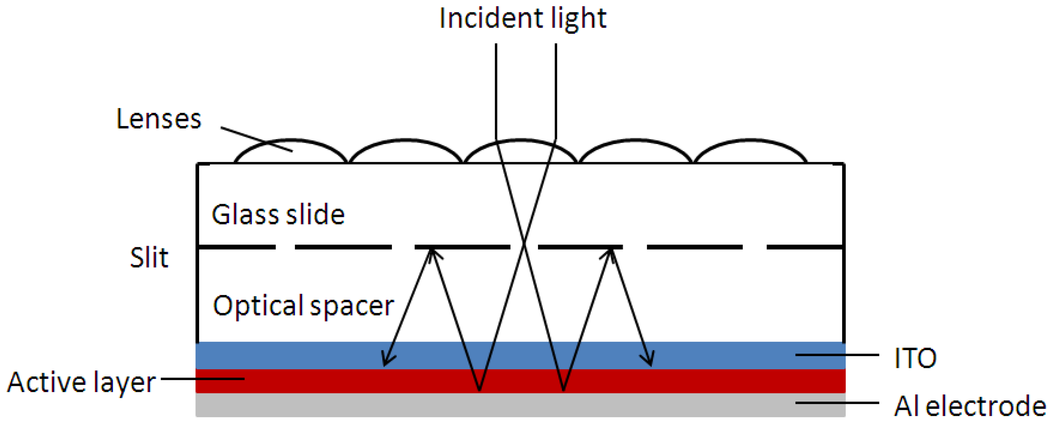
  125. Tvingstedt, K.; Dal Zilio, S.; Inganas, O.; Tormen, M. Trapping light with micro lenses in thin film organic photovoltaic cells. Opt. Exp. 2008, 16, 21608–21615. [Google Scholar] [CrossRef]
  126. Roman, L.S.; Inganäs, O.; Granlund, T.; Nyberg, T.; Svensson, M.; Andersson, M.R.; Hummelen, J.C. Trapping light in polymer photodiodes with soft embossed gratings. Adv. Mater. 2000, 12, 189–195. [Google Scholar] [CrossRef]
  127. Na, S.I.; Kim, S.S.; Jo, J.; Oh, S.H.; Kim, J.; Kim, D.Y. Efficient polymer solar cells with surface relief gratings fabricated by simple soft lithography. Adv. Funct. Mater. 2008, 18, 3956–3963. [Google Scholar] [CrossRef]
  128. Niggemann, M.; Glatthaar, M.; Gombert, A.; Hinsch, A.; Wittwer, V. Diffraction gratings and buried nano-electrodes--architectures for organic solar cells. Thin Solid Films 2004, 451-452, 619–623. [Google Scholar]
  129. Zilio, S.D.; Tvingstedt, K.; Inganäs, O.; Tormen, M. Fabrication of a light trapping system for organic solar cells. Microelectron. Eng. 2009, 86, 1150–1154. [Google Scholar] [CrossRef]
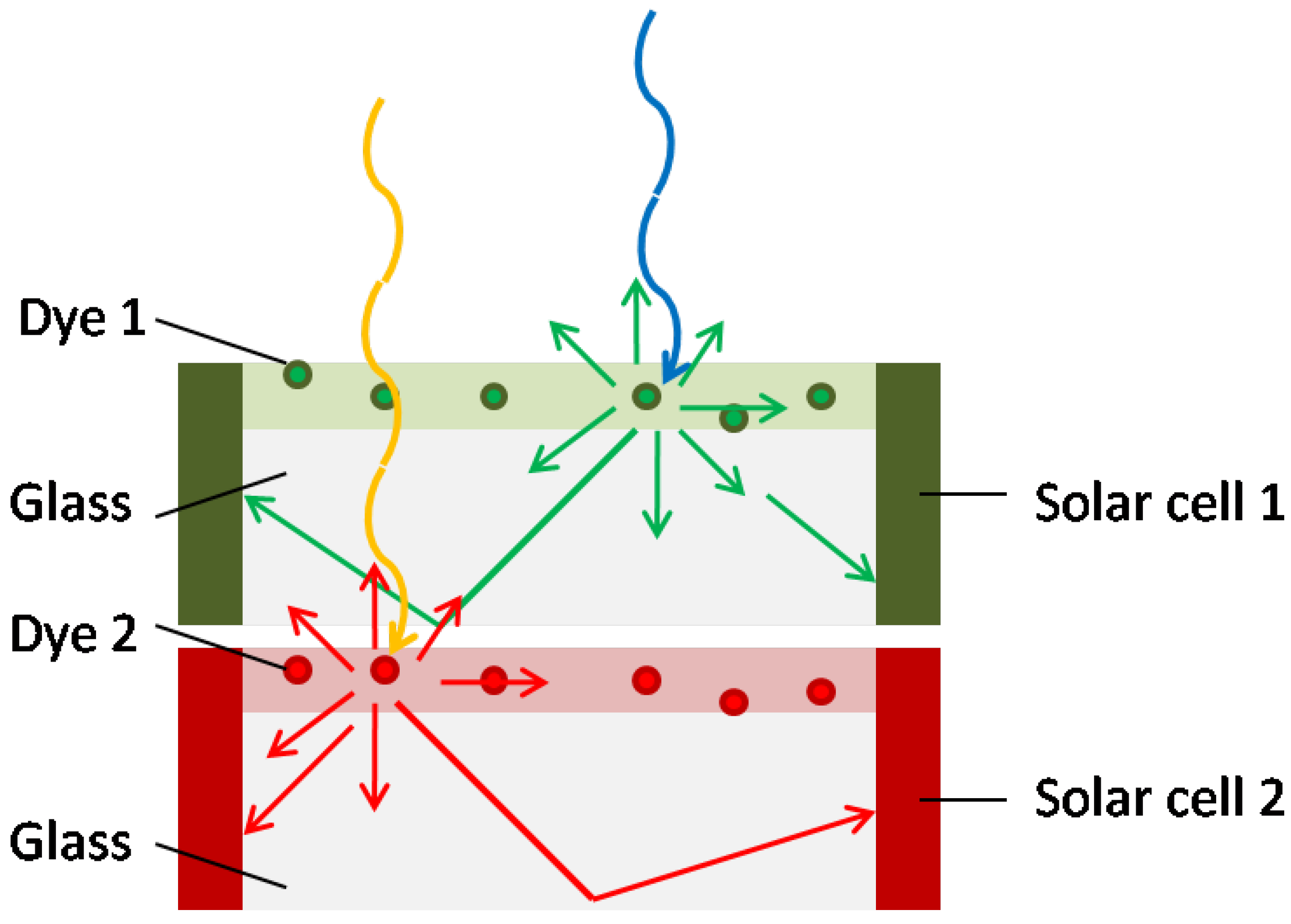
  130. Koeppe, R.; Sariciftci, N.S.; Buchtemann, A. Enhancing photon harvesting in organic solar cells with luminescent concentrators. Appl. Phys. Lett. 2007, 90, 181126. [Google Scholar] [CrossRef]
  131. Currie, M.J.; Mapel, J.K.; Heidel, T.D.; Goffri, S.; Baldo, M.A. High-efficiency organic solar concentrators for photovoltaics. Science 2008, 321, 226–228. [Google Scholar] [CrossRef] [PubMed]
  132. Rim, S.-B.; Zhao, S.; Scully, S.R.; McGehee, M.D.; Peumans, P. An effective light trapping configuration for thin-film solar cells. Appl. Phys. Lett. 2007, 91, 243501. [Google Scholar] [CrossRef]
  133. Tvingstedt, K.; Andersson, V.; Zhang, F.; Inganas, O. Folded reflective tandem polymer solar cell doubles efficiency. Appl. Phys. Lett. 2007, 91, 123514. [Google Scholar] [CrossRef]
  134. Andersson, V.; Tvingstedt, K.; Inganas, O. Optical modeling of a folded organic solar cell. J. Appl. Phys. 2008, 103, 7. [Google Scholar] [CrossRef]
  135. Andersson, B.V.; Persson, N.K.; Inganas, O. Comparative study of organic thin film tandem solar cells in alternative geometries. J. Appl. Phys. 2008, 104, 124508. [Google Scholar] [CrossRef]
  136. Curran, S.; Talla, J.; Dias, S.; Dewald, J. Microconcentrator photovoltaic cell (the m-C cell): Modeling the optimum method of capturing light in an organic fiber based photovoltaic cell. J. Appl. Phys. 2008, 104, 064305. [Google Scholar] [CrossRef]
  137. Liu, J.W.; Namboothiry, M.A.G.; Carroll, D.L. Optical geometries for fiber-based organic photovoltaics. Appl. Phys. Lett. 2007, 90, 133515. [Google Scholar] [CrossRef]
  138. O'Connor, B.; Pipe, K.P.; Shtein, M. Fiber based organic photovoltaic devices. Appl. Phys. Lett. 2008, 92, 193306. [Google Scholar] [CrossRef]

