Thermal Analysis of Power Rectifiers in Steady-State Conditions


1
Faculty of Electrical Engineering, Gheorghe Asachi Technical University of Iasi, Blvd, Dimitrie Mangeron, 21-23, Iasi 700050, Romania
2
Faculty of Engineering, Østfold University College, BRA Veien 4, 1671 Fredrikstad, Norway
*
Author to whom correspondence should be addressed.
Energies 2020, 13(8), 1942; https://doi.org/10.3390/en13081942
Submission received: 26 March 2020
/
Revised: 10 April 2020
/
Accepted: 12 April 2020
/
Published: 15 April 2020
(This article belongs to the Special Issue Power Converters, Electric Drives and Energy Storage Systems for Electrified Transportation and Smart Grid)
Abstract
:Power rectifiers from electrical traction systems, but not only, can be irreversibly damaged if the temperature of the semiconductor junction reaches high values to determine thermal runaway and melting. The paper proposes a mathematical model to calculate the junction and the case temperature in power diodes used in bridge rectifiers, which supplies an inductive-resistive load. The new thermal model may be used to investigate the thermal behavior of the power diodes in steady-state regime for various values of the tightening torque, direct current through the diode, airflow speed and load parameters (resistance and inductance). The obtained computed values were compared with 3D thermal simulation results and experimental tests. The calculated values are aligned with the simulation results and experimental data.
1. Introduction
A great challenge for power electronic systems is to remove the heat from the power devices in an efficient and cost-effective manner. Due to the needs of high power density and to the miniaturization of power converters, the components have to operate next to their thermal limits [1]. One of the main concerns in many power converters design procedure is to controlling the heat as the producer’s moves toward all-surface-mount implementations. Thus, in the early design phase of the power converters it is very important to understand the thermal aspects of the components in order to improve the devices thermal performances [2]. The available thermal models have their boundaries to correctly estimate the thermal behavior in the IGBTs: The usually used thermal models based on one-dimensional RC node have limits to estimate the temperature variation inside devices. A new lumped 3D thermal model is suggested in [3], which can be simply described from FEM simulations and may achieve the critical thermal distribution in long-term evaluations. The boundary constraints for the thermal investigations are considered, which may be adjusted to various real-field applications of power electronic converters. In the existing losses and thermal models, just the electrical loadings for design variables are considered. In [4], a full losses and thermal model taking into consideration the device rating as input variables is also presented. A mathematical relation between the power loss, thermal impedance and the silicon area for the IGBT is estimated. Thus, all the elements with impact over the loss and thermal aspects are considered with results in an optimal design of the power converter.
For the IGBT modules three usual thermal modeling methods regarding their influence on lifetime estimation are compared in [5]. It is shown that these models have important differences in estimating the cross-coupling terms between the chips in the module.
In [6], for a 1200 A, 3.3 kV IGBT module the thermal analysis is considered by the three-dimensional transmission line matrix method. The results show a three-dimensional visualization of self-heating in the module. The temperature evolution is determined during the PWM load cycles, with a good result regarding the thermal analysis and design. A mathematical modeling for time-variant cooling systems is considered in [7], switching between such networks matched to different edge conditions. The accuracy, in terms of temperature and predicted IGBT lifetime, for Foster and Cauer networks is analyzed and compared to errors in the thermal-interface-material resistance. A power electronic converter structure based on power losses and thermal models are considered in [8] for a three level active neutral point clamped voltage source converter using press-pack IGBT-diode pairs. The thermal model is based on water-cooled press-pack switches and is simulated for a 6 MW wind turbine grid interface.
The thermal management is an important aspect for the power converters used for vehicles. For the IGBT package modules employed in hybrid electric vehicle applications it is presented in [9] a method to obtain precise models for rapid electrothermal simulations with advantages in reducing the design cycle. For the traction motors, the volume of the motors can be decreased significantly by improving the thermal flows across the inductor. The silicone resin potted high power inductor for DC/DC switch-mode boost converters can be used [10] in comparison with classical air-cooled inductors, simulations and test being presented for a 40 kW DC–DC converter. In [11] is presented an experimental analysis of multichip IGBT package modules, combining rapid transient short-circuit electrical measurements with infrared thermal mapping considering realistic operating conditions. An electrothermal concise model of the multichip system is described, considering all the important operating and particular electrothermal effects, with application in the railway industry. An electrothermal mathematical model for a real-time thermal simulation of an IGBT in an inverter power module used on hybrid vehicle is considered with estimation of the temperature and power losses [12]. Thermal simulations were realized with high precision for a long real-time, which means more than 10 min, which is important for the vehicles. The peak torque for a traction motor is limited by switching device temperatures. For an 11 kW PMSM motor, it is presented in [13] a drive control strategy that merge the active thermal management model with dynamic DC-link voltage adaptation. Thus, the switching losses can be decreased at low speed by decreasing the bus voltage resulting a considerable inverter losses decrease at low speed.
Power converters for wind turbines are highly used due to the green energy evolution. Wind turbines are using power electronic converters with multichip paralleled IGBT modules. In [14], junction temperatures of chips for various positions with a better thermal coupling impedance model are estimated, and the outcomes are compared with the results of other thermal models.
A two-level power electronic converter for wind turbine is analyzed considering the losses and the junction temperature for the power devices in the case of a large wind speed variation, resulting in the high effect of the junction temperature over the operating point of the induction generator of the turbine [15,16].
Thermal characteristics of various power switching devices are considered in [17] for their impact on the thermal cycling of a 10 MW wind power converter in different working conditions considering IGBT modules and press-pack, the thermal characteristics of the power electronic converter being significantly changed according to the power semiconductor devices technology and their configurations.
In [18] is presented also an electrothermal model of an inverter but implemented in PLECS being used to estimate the IGBT junction temperature with a mission profile for a wind power application. The thermal network is determined from the heating curves of IGBT junction and case temperature that are measured on a power-cycling rig. Junction temperature is estimated with the power dissipation and thermal network. For rapid and precise thermal simulations of power semiconductor modules it is developed a Fourier-based solution, which can estimate the temperature versus time to resolve the heat equation in two dimensions [19], resulting a fast simulation compared to the finite-element (FEM).
Microchannel coolers for thermomechanical performance of power electronic modules with IGBT are analyzed in [20] by using finite element analysis with results in increasing the lifetime modules. Power loss model is used [21] to design a 3 kVA DC/AC high output power density converter considering a connection between the circuit stray parameters and the power losses into the converter. A thermal model of a heatsink as a RC thermal equivalent network that can be embedded in any circuit simulator, it is presented in [22]. The model considers thermal time constants of the heat sink, the convection cooling, thermal hotspots on the heatsink base plate, and thermal coupling between power semiconductor modules mounted onto the heatsink.
Design procedure considerations based on various temperature distribution study cases are realized on a prototype, a 2 kW integrated power electronic semiconductor modules using Cool MOS and SiC diode [23]. The thermal model is elaborated and the power dissipation of every power semiconductors in the active IPEM is calculated through the measurement-based power loss characteristics in datasheet. With the requirements of equal temperature distribution and light thermal interaction between power dice, the modification of temperature gradient distribution with the heat transfer coefficient of heatsink and die position is analyzed. In the [24] literature review for the design and study of thermal via in PCBs for thermal control of power electronic semiconductors lead to a selection for four different models for single power devices. The experimental results match the theoretical anticipation to identify the most effective thermal model via pattern.
For the estimation of the power module temperature field contours at various temperatures, a simplified 3D model of the power module was taken into consideration [25], and steady-state thermal analysis was done. The layout of the power electronic converter is optimized to decrease the heat distribution corresponding to the analysis outcome. The simulations show that an optimal distribution of the power supply module can increase the reliability of the switching mode DC/DC converters. The three-level active-neutral-point-clamped voltage source converter is used to defeat the uneven loss distribution [26]. The junction temperature and the load current of a power electronic converter system are obtained to calculate the power losses. The thermal resistance and the thermal capacitance of different components are used to express the thermal network, which is used to estimate the power device junction temperature, and to analyze transient thermal distribution.
In [27], it proposes the certainty design to the power electronic converter’s conventional compensation controller design with a new concept of a universal dual-loop controller, which uses temperature control loop as well as electric power control loop. The idea is based on a digital implementation of a variable load of power inverter system with real-time measurement approach of the chip’s surface temperature. The novelty is to get a better thermal control method of carrier frequency adjustment through experimental implementation during the full life cycle of the power electronic converter. A back-to-back 2-level/3-level inverter has been designed and developed such that the power will flow in both directions while the converter will perform better under arbitrary load conditions analyzing the thermal dissipation of the semiconductors [28]. The thermal investigation has been performed in the case of an IGBT module with a specifically integrated real time current controller. In [29] it is proposed to use the active thermal management to reduce the switching losses during transient regime in order to assure a high current without overcoming the temperature limits, reducing the overdesign of power converters.
An electrothermal design methodology is proposing and a reliability study is realized [30] for converters used for photovoltaic application, which is the distributed maximum power point tracking converter. In [31] is presented an electrothermal analysis based on the reduced order modeling technique in which the zero-dimensional thermal network is obtained from the three-dimensional IGBT semiconductor module packaging structure and incorporated with the electrothermal model of the chips.
Considering the previous works of different research teams, it can be outlined that the existing thermal models have their limits to predict the thermal behavior of different types of power semiconductor devices, especially in the case of IGBTs. It has been proposed simplified 3D thermal models based on FEM and also the well-known Foster and Cauer networks to analyze inverters’ behavior from thermal point of view. More, the researchers developed different methods to monitor the junction temperature of the IGBTs with the aim to check their reliability.
The aim of this paper is to investigate the thermal behavior of the power diodes from a rectifier bridge used in electrical traction during steady-state conditions.
The paper is arranged as follows, in Section 2 the mathematical model to calculate the junction and case temperature will be developed. Then, in Section 3, the calculated values will be compared with the simulated results of a 3D thermal model of a power assembly, which includes two power diodes mounted on the heatsink. Finally, the proposed mathematical model will be validated through a series of experimental tests, in Section 4 followed by the conclusion section, where the most important outcomes of the paper are highlighted.
2. Mathematical Model
The goal of the thermal analysis is to establish a mathematical model that will be used to compute the junction and the case temperature for a power diode, which is the main component from a power traction rectifier. The power loss of the diode during steady-state conditions is a sum of the following terms:
where:
- PF means the power loss during direct conduction;
- PR is the power loss in the case of locked conditions;
- Pc is the power loss during commutations.
In the situation of direct conduction, the power losses can be calculated using the following expression,
and it is the observed that depends both on diode intrinsic characteristics through the parameters VT and rT, and current waveform which flows through the power diode. In the case of a resistive inductive load, the electric current can be described by the next formula,
Thus, it results in the RMS current:
Additionally, the average current has the expression,
Therefore, considering the expressions of the RMS Equation (4) and average Equation (5), the relation to calculate the power losses during direct conduction, becomes,
The power losses in the case of locked conditions PR can be calculated by the product between the maximum reverse current IRM and the maximum repetitive reverse voltage VRRM,
Both parameters IRM and VRRM depend on the type of the power diode and their values are depicted in the datasheet of the diode. The commutation power loss Pc can be calculated using the following relation,
where the maximum reverse voltage VRmax depends on the type of the power rectifier topology. It has been considered a B6 bridge rectifier. In this case, the maximum reverse voltage is equal with the secondary voltage of the supply transformer, multiplied by the coefficient .
In the case of traction power rectifiers, the diodes are mounted on aluminum heatsinks with the aim to ensure an efficient cooling of the semiconductor junction. Thus, the main components of the current path within the power assembly of the bridge rectifier, includes power diode, heatsink and busbar. Therefore, in addition to the power loss of the diode P, there are also the power losses of the contact resistance between the case diode and the heatsink as main component of the current path. The power loss because of the contact resistance can be computed with the known formula,
Further, it has been examined the case in which the rectifier bridge is composed from power diodes type SKN 300 threaded stud M16 × 1.5 mm. There is an inverse proportional relationship between the contact resistance Rc and the contact force F, which will be calculated knowing the tightening torque M, the screw diameter d, the thread pitch p and the friction coefficient μ, with the following formula [32],
The nonlinear variation between contact resistance Rc and contact force F can be represented by a mathematical function. Starting from an experimental dataset, the curve of the contact resistance has been fitted to the following expression,
The coefficients of the fitting curve have the next values: a1 = 397.53, b1 = 0.98625 and c1 = 0.00011. The comparison between experimental and fitting curve of the contact resistance variation vs. contact force is presented in the Figure 1.
Thus, using the expressions (4), (10) and (11), the contact power losses can be computed as follows,
Finally, the total power loss considering both diode power loss and contact power loss has the expression:
After the previous expressions (6), (7), (8) and (12) have been replaced in the above relation, we obtained the diode total power dissipated as:
The above expression regarding the calculation of the total power dissipated at the power diode will be used to determine the junction and case temperature of the analyzed power diode. The following calculation formulas can be used to get the values for the junction temperature,
and for the case temperature of the power diode,
The values of the junction-case and case-heatsink thermal resistance can be obtained from the power diode datasheets. Thus, in the case of SKN 300 power diode, the following values were identified: Rthjc = 0.15 °C/W and Rthck = 0.02 °C/W. Generally, the heatsink-environment thermal junction was not a constant value and it depended on the cooling method (forced or natural) and the heatsink type. The heatsink datasheets present variation curves of the heatsink-environment thermal junction vs. air speed. The cooling of the SKN 300 power diode can be provided by aluminum heatsink type R150-E50 manufactured by IPRS Baneasa. From the datasheet, it can be obtained the nonlinear variation of heatsink-environment thermal resistance vs. air speed. This curve can be approximated with the following mathematical expression:
where the parameters of the fitting curve, are: a2 = 0.25035; b2 = −0.015359, c2 = 0.006483 and d2 = −0.189932. The normal variation of decreased heatsink-environment thermal resistance for increasing air speed can be observed in Figure 2.
So, the junction and case temperature of the power diode will be calculated using the next expressions:
and,
By replacing in the above formulas, the expression of the total power loss, the calculation relations for the junction and case temperature are finally obtained:
and,
The above expressions outline that both case and junction temperature depends on conduction current, tightening torque, load resistance, load inductance and air speed.
3. Three-Dimensional Thermal Model
The thermal analysis has been focused on a power assembly made from two stud rectifier diodes type SKT 340 mounted on the same aluminum heatsink. Actually, the power assembly can be considered as one of the three legs from the three-phase full- bridge rectifier, which provides a DC current on a resistive-inductive load. The datasheet of the rectifier diode outlines the following values for the main parameters of the diode: VT = 0.8 V, rT = 0.6 mΩ, IRM = 60 mA, VRRM = 1200 V and Qs = 200 μC. Considering the direct current through the power diode with the RMS value of 250 A, it can be calculated the power loss within the diode, which had the value of 119.29 W. In the case of the recommended tightening torque of 30 Nm, the contact resistance had the value of 0.45 mΩ. Thus, for the same value of the direct current flowing through the diode, the power loss because of the contact resistance between heatsink and the diode was about 28.125 W.
The structure of the power diode was highlighted by a solid copper hexagon with a threaded stud, which is used to bolt the component onto a heatsink and discharge the heat produced by the chip. A glass or ceramic cap with a bushing for the cathode terminal provides hermetical case sealing. Case parts are attached by welding or brazing. The chip is straightly soldered onto the disk made of molybdenum to prevent high mechanical pressure in the semiconductor as a result of important differences in the expansion coefficients for silicon and copper. In order to achieve the three-dimensional geometry of the analyzed power assembly, the Pro/Engineering software package has been used. The thermal model included only the components that actively participate in the heat transfer from the power diode to the environment through the heatsink. These components are (Figure 3) the copper braid, molybdenum discs, Silicom chip, solid copper hexagon with threated stud and aluminum heatsink. Due to the fact that the ceramic housing participates in a very low weight to the heat transfer from the silicon chip to the environment, it was not included in the thermal model.
The material characteristics of each component part of the power diode and the heatsink are synthesized in the Table 1 and the complete thermal model of the power assembly is shown in Figure 4.
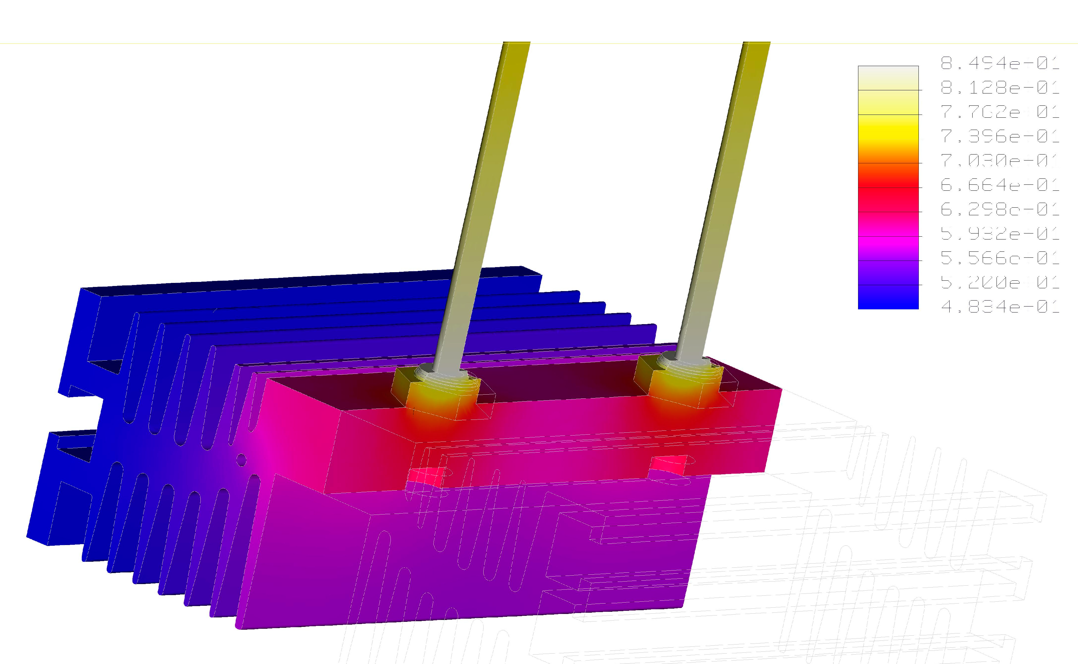
On the basis of Pro-MECHANICA software package, some thermal simulations were performed during steady-state conditions. The temperature profile of the power diode, in the case of tightening torque of 30 Nm, air speed value of 1 m/s, direct current of 200 A and the load with a resistance of 20 Ω and inductance about 60 mH, is presented in the next pictures, Figure 5 and Figure 6. It can be seen a maximum temperature of the power assembly about 84.94 °C on the silicon chip of the diode and a minimum temperature of 48.34 °C on the heatsink outer surfaces.
The heat load because of the diode power loss has been applied within the volume of the silicon chip considering a uniform spatial distribution. In addition, it was considered the power loss of the contact resistance between stud copper base of the diode and the heatsink. This additional heat load was applied on the outer surface of the copper screw. It was assumed an ambient temperature about 23 °C. The value of the convection coefficient, 12.35 W/m2°C, was obtained from experimental tests. The outer surfaces of the heatsink were considered as boundary conditions, so that heat transfer by convection could be applied. It was considered a uniform spatial distribution of the convection coefficient on all outer surfaces of the heatsink and a bulk temperature of 23 °C was applied.
4. Discussion of the Results
Further on, considering the obtained solutions for the calculation of junction and case temperature of the power diode from the Equation (20), respectively (21), the influence of the direct current, airflow speed and load parameters on thermal behavior of the power diode would be investigated.
The first thermal analysis refers to the variation of junction and case temperature of the power diode against tightening torque at different current values of 200, 250 and 300 A, in the case of airflow speed of 1 m/s, load resistance about 20 Ω and load inductance of 60 mH. It can be seen a decrease in both junction and case temperatures, Figure 7 and Figure 8, when the tightening torques increases. This can be explained because as torque increases, then the contact force between case diode and heatsink increases, which leads to lower values of the contact resistance and contact power loss, and finally, the junction and case temperature values will decrease. For instance, when tightening torque had the value of 15 Nm, the junction temperature was 109.4 °C, Figure 7, and for a torque value of 50 Nm, the junction temperature reached the value of 104.24 °C, so, a difference about 5 °C. For the same variation of the tightening torque, from 15 to 50 Nm, the case temperature decreases from 76.28 to 73.03 °C, Figure 8. At both junction and case temperature variation, the simulated values are placed on the same graph. It can be noticed that thermal simulation values were lower than the calculated ones. This can be explained because the mathematical model of junction and case temperature took into account a concentrated power loss both for power diode and contact resistance. Actually, during thermal simulations, the power loss was evenly distributed on silicon chip and contact surface between stud diode and heatsink. This led to an improved heat transfer from the power assembly to the environment, and finally, lower junction and case temperatures compared to those calculated. For instance, in the case of tightening torque of 30 Nm and 300 A, Figure 7, the simulated junction temperature was 105.1 °C, a lower value than 105.95 °C for the calculated temperature and the simulated case temperature was 73.2 °C lower than 74.11 °C, the calculated one, Figure 8.
A series of experimental tests were performed in order to validate the proposed mathematical model to calculate the junction and case temperature of power diode. A three-phase bridge rectifier with forced cooling supplied through the power transformer Tr it was considered, as can be seen in Figure 9. The main goal was to acquire the case temperatures of the power diode mounted on the aluminum heatsink. The temperature values were acquired with suitable thermocouple Th type K. It used an electronic board AS type AT2 F-16 in order to adapt the small signals provided by thermocouples to the data acquisition board type PC-LPM-16. This can be programmed by LabVIEW software. The current value can be recorded using the ammeter A.
From the graph of case temperature variation, Figure 8, it can be noticed that experimental values were higher than the calculated ones. This is explained because the mathematical model considers a uniform cooling of the power diode case. Actually, the airflow did not uniformly cool the surface of the diode case due to the mounting technology of the cooling system for the bridge rectifier. Hence, there was not a good heat transfer from the case to the environment. As an example, in the case of tightening torque of 30 Nm and direct current of 300 A, the experimental case temperature of 75 °C was higher than 74.11 °C, the calculated value.
The second thermal analysis takes into account the junction and case temperature variation against tightening torque for different load resistance values (10, 20 and 100 Ω) when the direct current was 300 A, airflow speed of 1 m/s and load inductance of 10 mH. It can be noticed the decreasing of both junction and case temperature when the torque increased, Figure 10 and Figure 11. The explanation was the same as in previous analyzed case.
In addition, it can be noticed that for higher values of the load resistance, the temperature values decreased. This can be explained because as load resistance increases than the impedance increases and the current decreases, which finally leads to lower power loss and lower junction and case temperatures. For instance, at 30 Nm tightening torque, and 10 Ω load resistance, the junction temperature was 94.67 °C in comparison with the case of 100 Ω load resistance when the junction temperature got the value of 93.11 °C, Figure 10. At the same tightening torque of 30 Nm, the case temperature was 67.01 °C when load resistance was 10 Ω and became 66.03 °C for a load resistance of about 100 Ω, Figure 11. The same as in the previous analyzed case, the simulation values were lower than the calculated junction and case temperatures. As an example, at 15 Nm tightening torque and 10 Ω load resistance, the simulated value was 96.9 °C with respect to 97.72 °C of the calculated junction temperature, Figure 10, and the simulated case temperature was 68.4 °C lower than 68.93 °C, the calculated one. Moreover, on the same graph of case temperature variation, there were placed the experimental data, which were higher than the computed ones, Figure 11. The explanation was the same as in previous case. As an example, at 30 Nm tightening torque and 10 Ω load resistance, the experimental value was 67.4 °C with respect to 67 °C of the calculated case temperature.
The next thermal analysis considered the same variation of junction and case temperature against tightening torque but at different load inductance values from 10 to 160 mH, in the case of a direct current of 300 A, airflow speed of 1 m/s and load resistance of 100 Ω. As in the previous analyzed cases, the temperatures decreased when the tightening torque increased, Figure 12 and Figure 13. For instance, in the case of a load inductance of 10 mH, the junction temperature decreased from 96.14 (torque of 15 Nm) to 91.81 °C (torque of 50 Nm), Figure 12, and the case temperature decreased from 67.93 (torque of 15 Nm) to 65.09 °C (torque of 50 Nm), Figure 13. Regarding the simulated temperature values, the same trend was confirmed: lower values than those calculated. For instance, in the case of tightening torque of 30 Nm and load inductance of 160 mH, the simulated junction temperature had a lower value of 96.6 °C than 97.08 °C the calculated one, Figure 12 and the simulated case temperature was 67.9 °C lower than 68.53 °C obtained from computations, Figure 13. On the same graph, it can be noticed also the obtained experimental values, which were higher than the calculated ones. For instance, at 30 Nm tightening torque and load inductance of 160 mH, the experimental case value was 68.9 °C with respect to 68.53 °C, the calculated one.
The last thermal analysis investigated the variation of junction and case temperature at different airflow speed values from 2 to 6 m/s when the direct current had the value of 300 A, the load resistance was about 10 Ω and the load inductance was 60 mH. The same decreasing evolution of the temperatures when the tightening torque increased could be observed, both for junction and case temperature, Figure 14 and Figure 15.
As an example, in the case of the air speed value of 2 m/s, at a torque value of 15 Nm there was a junction temperature of 119.07 °C and case temperature of 75.87 °C, and to a torque value of 50 Nm, the junction temperature reached the value of 113.49 °C and the case temperature got a value of 72.72 °C. As in previous analyzed cases, the simulated values of the junction and case temperature were lower than the computed ones: a junction temperature of 114.7 °C in comparison with the calculated value of 115.34 °C in the case of 30 Nm tightening torque, Figure 14, and a case temperature of 72.9 °C lower than 73.36 °C, the calculated value for the same tightening torque, Figure 15. Additionally, on the last graph, it can be noticed the experimental values for the case temperature, which were higher than the calculated ones. For instance, in the case of air speed value of 2 m/s and a torque value of 30 Nm, the experimental obtained value of the case temperature was 74.4 °C with respect to the calculated one of 73.36 °C.
The difference between calculated and experimental values was also due to measurement errors, simplifications in the mathematical model and experimental setup. It could be noticed that the maximum difference between calculated and measured values was less than 2 °C.
5. Conclusions
A new mathematical model to investigate the power diodes’ behavior from a thermal point of view was proposed in this paper. The power diodes belonged to a three-phase bridge rectifier used in electric traction applications. The mathematical model can be used to calculate the junction and case temperature of the power diode for different values of the tightening torque, direct current through the diode, airflow speed and load parameters (resistance and inductance). It outlined the decreasing of both the junction and case temperature when the tightening torque increased. The decrease in temperature was at a maximum of 5 °C while the tightening torque increased more than 3 times from 15 to 50 Nm.
The computed values were compared with the simulation results. Hence, a 3D modeling and thermal simulations of a power assembly including two diodes mounted on the heatsink were performed. The thermal simulation values were lower that the calculated ones because the because the mathematical model of junction temperature took into account a concentrated power loss and during thermal simulations, the power loss was evenly distributed on the silicon chip and contact surface, which led to a better heat transfer to the environment. Additionally, the calculated values were compared with some experimental data. It recorded higher experimental values than the calculated ones because the mathematical model considered a uniform cooling of the power diode case and actually, the airflow did not uniformly cool the surface of the diode case, which did not lead to a good heat transfer to the environment.
The proposed thermal model can be used to design different power bridge rectifiers from electric traction but not only this, with an optimized thermal distribution it can also consider the influence of some key parameters both electrical and mechanical. Since the new mathematical model takes into account also some thermal parameters, as thermal resistances related to power diode and heatsink, it can be customized for a wide range of power semiconductor devices mounted on different type of heatsinks from power converters.
Author Contributions
The whole article has been performed by the authors with equal contribution. All authors have read and agree to the published version of the manuscript.
Funding
This research received no external funding.
Acknowledgments
The authors had not received any funds for covering the costs to publish in open access.
Conflicts of Interest
The authors declare no conflict of interest.
Nomenclature
| θj | means the junction temperature °C |
| θc | case temperature °C |
| θa | ambient temperature °C |
| P | average power loss W |
| rT | internal resistance Ω |
| VT | voltage drop V |
| Rthjc | thermal resistance between junction and case °C/W |
| Rthck | thermal resistance between case and heatsink °C/W |
| Rthka | thermal resistance between heatsink and environment °C/W |
| IFAV | average current A |
| IRMS | root mean square value of the current A |
| Im | maximum current A |
| IRM | maximum reverse current A |
| VR | reverse voltage V |
| VRRM | maximum repetitive reverse voltage V |
| U2 | secondary voltage V |
| ϕ | phase shift between the current and voltage °el |
| f | commutation frequency Hz |
| Qs | recovery charge C |
| ω | pulse current rad/s |
| L | inductance H |
| R | resistance Ω |
| vair | air speed m/s |
| Rc | contact resistance Ω |
| F | contact force N |
| M | tightening torque Nm |
| d | screw diameter m |
| p | thread pitch m |
| μ | friction coefficient |
References
- Shafaei, R.; Ordonez, M.; Saket, M.A. Three-dimensional frequency-dependent thermal model for planar transformers in LLC resonant converters. IEEE Trans. Power Electron. 2018, 34, 4641–4655. [Google Scholar] [CrossRef]
- Bulut, Y.; Pandya, K. Thermal modeling for power MOSFETs in DC/DC applications. In Proceedings of the 5th International Conference on Thermal and Mechanical Simulation and Experiments in Microelectronics and Microsystems, EuroSimE 2004, Brussels, Belgium, 10–12 May 2004; IEEE: Piscataway, NJ, USA, 2004; pp. 429–433. [Google Scholar]
- Bahman, A.S.; Ma, K.; Blaabjerg, F. A lumped thermal model including thermal coupling and thermal boundary conditions for high-power IGBT modules. IEEE Trans. Power Electron. 2017, 33, 2518–2530. [Google Scholar] [CrossRef]
- Ma, K.; Bahman, A.S.; Beczkowski, S.; Blaabjerg, F. Complete loss and thermal model of power semiconductors including device rating information. IEEE Trans. Power Electron. 2014, 30, 2556–2569. [Google Scholar] [CrossRef]
- Poller, T.; D’Arco, S.; Hernes, M.; Lutz, J. Influence of thermal cross-couplings on power cycling lifetime of IGBT power modules. In Proceedings of the 2012 7th International Conference on Integrated Power Electronics Systems (CIPS), Nuremberg, Germany, 6–8 March 2012; IEEE: Piscataway, NJ, USA, 2012; pp. 1–6. [Google Scholar]
- Hocine, R.; Pulko, S.H.; Stambouli, A.B.; Saidane, A. TLM method for thermal investigation of IGBT modules in PWM mode. Microelectron. Eng. 2009, 86, 2053–2062. [Google Scholar] [CrossRef]
- Gradinger, T.; Riedel, G. Thermal networks for time-variant cooling systems: Modeling approach and accuracy requirements for lifetime prediction. In Proceedings of the 2012 7th International Conference on Integrated Power Electronics Systems (CIPS), Nuremberg, Germany, 6–8 March 2012; IEEE: Piscataway, NJ, USA, 2012; pp. 1–6. [Google Scholar]
- Senturk, O.S.; Helle, L.; Munk-Nielsen, S.; Rodriguez, P.; Teodorescu, R. Converter structure-based power loss and static thermal modeling of the press-pack IGBT three-level ANPC VSC applied to multi-MW wind turbines. IEEE Trans. Ind. Appl. 2011, 47, 2505–2515. [Google Scholar] [CrossRef]
- Ciappa, M.; Fichtner, W.; Kojima, T.; Yamada, Y.; Nishibe, Y. Extraction of accurate thermal compact models for fast electro-thermal simulation of IGBT modules in hybrid electric vehicles. Microelectron. Reliab. 2005, 45, 1694–1699. [Google Scholar] [CrossRef]
- You, B.G.; Lee, B.K.; Lee, S.W.; Jeong, M.C.; Kim, J.H.; Jeong, I.B. Improvement of the thermal flow with potting structured inductor for high power density in 40kW DC-DC converter. In Proceedings of the 2012 IEEE Vehicle Power and Propulsion Conference, Seoul, South Korea, 9–12 October 2012; IEEE: Piscataway, NJ, USA, 2012; pp. 1027–1032. [Google Scholar]
- Castellazzi, A.; Johnson, M.; Piton, M.; Mermet-Guyennet, M. Experimental analysis and modeling of multi-chip IGBT modules short-circuit behavior. In Proceedings of the 2009 IEEE 6th International Power Electronics and Motion Control Conference, Wuhan, China, 17–20 May 2009; IEEE: Piscataway, NJ, USA, 2009; pp. 285–290. [Google Scholar]
- Zhou, Z.; Kanniche, M.S.; Butcup, S.G.; Igic, P. High-speed electro-thermal simulation model of inverter power modules for hybrid vehicles. IET Electr. Power Appl. 2011, 5, 636–643. [Google Scholar] [CrossRef]
- Lemmens, J.; Driesen, J.; Vanassche, P. Dynamic DC-link voltage adaptation for thermal management of traction drives. In Proceedings of the 2013 IEEE Energy Conversion Congress and Exposition, Denver, CO, USA, 15–19 September 2013; IEEE: Piscataway, NJ, USA; pp. 180–187. [Google Scholar]
- Honsberg, M.; Radke, T. 3-level IGBT modules with trench gate IGBT and their thermal analysis in UPS, PFC and PV operation modes. In Proceedings of the 2009 13th European Conference on Power Electronics and Applications, Barcelona, Spain, 8–10 September 2009; IEEE: Piscataway, NJ, USA, 2009; pp. 1–7. [Google Scholar]
- Zhou, D.; Blaabjerg, F.; Lau, M.; Tonnes, M. Thermal cycling overview of multi-megawatt two-level wind power converter at full grid code operation. IEEJ J. Ind. Appl. 2013, 2, 173–182. [Google Scholar] [CrossRef] [Green Version]
- Zhou, D.; Blaabjerg, F.; Lau, M.; Tonnes, M. Thermal analysis of multi-MW two-level wind power converter. In Proceedings of the IECON 2012–38th Annual Conference on IEEE Industrial Electronics Society, Montreal, QC, Canada, 25–28 October 2012; IEEE: Piscataway, NJ, USA, 2012; pp. 5858–5864. [Google Scholar]
- Ma, K.; Blaabjerg, F. The impact of power switching devices on the thermal performance of a 10 MW wind power NPC converter. Energies 2012, 5, 2559–2577. [Google Scholar] [CrossRef] [Green Version]
- Huang, H.; Bryant, A.T.; Mawby, P.A. Electro-thermal modelling of three phase inverter. In Proceedings of the 2011 14th European Conference on Power Electronics and Applications, Birmingham, UK, 30 August–1 September 2011; IEEE: Piscataway, NJ, USA, 2011; pp. 1–7. [Google Scholar]
- Swan, I.R.; Bryant, A.T.; Mawby, P.A. Fast thermal models for power device packaging. In Proceedings of the 2008 IEEE Industry Applications Society Annual Meeting, Edmonton, AB, Canada, 5–9 October 2008; IEEE: Piscataway, NJ, USA, 2008; pp. 1–8. [Google Scholar]
- Xu, L.; Liu, Y.; Liu, S. Modeling and simulation of power electronic modules with microchannel coolers for thermo-mechanical performance. Microelectron. Reliab. 2014, 54, 2824–2835. [Google Scholar] [CrossRef]
- Graditi, G.; Adinolfi, G.; Tina, G.M. Photovoltaic optimizer boost converters: Temperature influence and electro-thermal design. Appl. Energy 2014, 115, 140–150. [Google Scholar] [CrossRef]
- Drofenik, U.; Kolar, J.W. A thermal model of a forced-cooled heat sink for transient temperature calculations employing a circuit simulator. IEEJ Trans. Ind. Appl. 2006, 126, 841–851. [Google Scholar] [CrossRef] [Green Version]
- Chen, Q.; Yang, X.; Wang, Z.; Zhang, L.; Zheng, M. Thermal design considerations for integrated power electronics modules based on temperature distribution cases study. In Proceedings of the 2007 IEEE Power Electronics Specialists Conference, Orlando, FL, USA, 17–21 June 2007; IEEE: Piscataway, NJ, USA, 2007; pp. 1029–1035. [Google Scholar]
- Gautam, D.S.; Musavi, F.; Wager, D.; Edington, M. A comparison of thermal vias patterns used for thermal management in power converter. In Proceedings of the 2013 IEEE Energy Conversion Congress and Exposition, Denver, CO, USA, 15–19 September 2013; IEEE: Piscataway, NJ, USA, 2013; pp. 2214–2218. [Google Scholar]
- Gao, C.; Liu, H.; Huang, J.; Diao, S. Steady-state thermal analysis and layout optimization of DC/DC converter. In Proceedings of the 2014 Prognostics and System Health Management Conference (PHM-2014 Hunan), Zhangiiaijie, China, 24–27 August 2014; IEEE: Piscataway, NJ, USA, 2014; pp. 405–409. [Google Scholar]
- Cheng, L.; Chen, Q.; Li, G.; Hu, C.; Zheng, C.; Fang, G. Electro-thermal loss analysis of the 3L-ANPC converter. In Proceedings of the 2014 IEEE 5th International Symposium on Power Electronics for Distributed Generation Systems (PEDG), Galway, Ireland, 24–27 June 2014; IEEE: Piscataway, NJ, USA, 2014; pp. 1–5. [Google Scholar]
- Zhou, L.; Wu, J.; Sun, P.; Du, X. Junction temperature management of IGBT module in power electronic converters. Microelectron. Reliab. 2014, 54, 2788–2795. [Google Scholar] [CrossRef]
- Li, H.; Liao, X.; Li, Y.; Liu, S.; Hu, Y.; Zeng, Z.; Ran, L. Improved thermal couple impedance model and thermal analysis of multi-chip paralleled IGBT module. In Proceedings of the 2015 IEEE Energy Conversion Congress and Exposition, Montreal, QC, Canada, 20–24 September 2015; IEEE: Piscataway, NJ, USA, 2015; pp. 3748–3753. [Google Scholar]
- Andresen, M.; Liserre, M. Impact of active thermal management on power electronics design. Microelectron. Reliab. 2014, 54, 1935–1939. [Google Scholar] [CrossRef] [Green Version]
- Hayashi, Y.; Takao, K.; Adachi, K.; Ohashi, H. Design consideration for high output power density (OPD) converter based on power-loss limit analysis method. In Proceedings of the 2005 European Conference on Power Electronics and Applications, Dresden, Germany, 11–14 September 2005; IEEE: Piscataway, NJ, USA, 2005; pp. 1–9. [Google Scholar]
- Li, X.; Li, D.; Qi, F.; Packwood, M.; Luo, H.; Liu, G.; Dai, X. Advanced Electro-Thermal Analysis of IGBT Modules in a Power Converter System. In Proceedings of the 2019 20th International Conference on Thermal, Mechanical and Multi-Physics, Hannover, Germany, 24–27 March 2019; IEEE: Piscataway, NJ, USA, 2019; pp. 1–4. [Google Scholar]
- Groover, M.P. Fundamentals of Modern Manufacturing: Materials, Processes and Systems, 4th ed.; John Wiley & Sons, Inc.: Hoboken, NJ, USA, 2010; ISBN 978-0470-467002. [Google Scholar]
Figure 1.
Contact resistance Rc vs. contact force F. Comparison between experimental (Rc_exp) and fitting curve (Rc_fit).
Figure 1.
Contact resistance Rc vs. contact force F. Comparison between experimental (Rc_exp) and fitting curve (Rc_fit).

Figure 2.
Heatsink-environment thermal resistance vs. air speed. Comparison between datasheet and fitting curve.
Figure 2.
Heatsink-environment thermal resistance vs. air speed. Comparison between datasheet and fitting curve.

Figure 3.
3D geometry of the power diode thermal model: 1—copper braid; 2—molybdenum disc; 3—silicon chip; 4—molybdenum disc; 5—solid copper hexagon with threaded stud and 6—heatsink.
Figure 3.
3D geometry of the power diode thermal model: 1—copper braid; 2—molybdenum disc; 3—silicon chip; 4—molybdenum disc; 5—solid copper hexagon with threaded stud and 6—heatsink.

Figure 4.
3D geometry thermal model of the power assembly power diodes heatsink.

Figure 5.
Temperature distribution of the power assembly. Cross-section through both power diodes.

Figure 6.
Temperature distribution of the power assembly. Cross-section through only one power diode.
Figure 6.
Temperature distribution of the power assembly. Cross-section through only one power diode.

Figure 7.
Junction temperature variation for different current values: 200, 250 and 300 A (v = 1 m/s, R = 20 Ω and L = 60 mH).
Figure 7.
Junction temperature variation for different current values: 200, 250 and 300 A (v = 1 m/s, R = 20 Ω and L = 60 mH).

Figure 8.
Case temperature variation for different current values: 200, 250 and 300 A (v = 1 m/s, R = 20 Ω and L = 60 mH).
Figure 8.
Case temperature variation for different current values: 200, 250 and 300 A (v = 1 m/s, R = 20 Ω and L = 60 mH).

Figure 9.
Experimental setup.

Figure 10.
Junction temperature variation for different load resistance values: 10, 20 and 100 Ω (v = 1 m/s, I = 300 A and L = 10 mH).
Figure 10.
Junction temperature variation for different load resistance values: 10, 20 and 100 Ω (v = 1 m/s, I = 300 A and L = 10 mH).

Figure 11.
Case temperature variation for different load resistance values: 10, 20 and 100 Ω (v = 1 m/s, I = 300 A and L = 10 mH).
Figure 11.
Case temperature variation for different load resistance values: 10, 20 and 100 Ω (v = 1 m/s, I = 300 A and L = 10 mH).

Figure 12.
Junction temperature variation for different load inductance values: 10, 100 and 160 mH (v = 1 m/s, I = 300 A and R = 100 Ω).
Figure 12.
Junction temperature variation for different load inductance values: 10, 100 and 160 mH (v = 1 m/s, I = 300 A and R = 100 Ω).

Figure 13.
Case temperature variation for different load inductance values: 10, 100 and 160 mH (v = 1 m/s, I = 300 A and R = 100 Ω).
Figure 13.
Case temperature variation for different load inductance values: 10, 100 and 160 mH (v = 1 m/s, I = 300 A and R = 100 Ω).

Figure 14.
Junction temperature variation for different air speed values: 2, 4 and 6 m/s (I = 300 A, R = 10 Ω and L = 60 mH).
Figure 14.
Junction temperature variation for different air speed values: 2, 4 and 6 m/s (I = 300 A, R = 10 Ω and L = 60 mH).

Figure 15.
Case temperature variation for different air speed values: 2, 4 and 6 m/s (I = 300 A, R = 10 Ω and L = 60 mH).
Figure 15.
Case temperature variation for different air speed values: 2, 4 and 6 m/s (I = 300 A, R = 10 Ω and L = 60 mH).


Table 1.
Material data of power diode and heatsink.
| Parameter | Material | |||
|---|---|---|---|---|
| Copper | Silicon | Molybdenum | Aluminum | |
| γ (kg/m3) | 8900 | 2330 | 10220 | 2700 |
| c (J/kg°C) | 387 | 702 | 255 | 900 |
| λ (W/m°C) | 385 | 124 | 138 | 200 |
© 2020 by the authors. Licensee MDPI, Basel, Switzerland. This article is an open access article distributed under the terms and conditions of the Creative Commons Attribution (CC BY) license (http://creativecommons.org/licenses/by/4.0/).
Share and Cite
MDPI and ACS Style
Plesca, A.; Mihet-Popa, L. Thermal Analysis of Power Rectifiers in Steady-State Conditions. Energies 2020, 13, 1942. https://doi.org/10.3390/en13081942
AMA Style
Plesca A, Mihet-Popa L. Thermal Analysis of Power Rectifiers in Steady-State Conditions. Energies. 2020; 13(8):1942. https://doi.org/10.3390/en13081942
Chicago/Turabian StylePlesca, Adrian, and Lucian Mihet-Popa. 2020. "Thermal Analysis of Power Rectifiers in Steady-State Conditions" Energies 13, no. 8: 1942. https://doi.org/10.3390/en13081942
Note that from the first issue of 2016, this journal uses article numbers instead of page numbers. See further details here.