


Abstract
Grid-connected and grid-forming inverters play essential roles in the utilization of renewable energy. One problem of such a converter system is the voltage deviations in the DC-link between the source and the inverter that can disrupt the inverter output voltage. A common method to prevent these voltage deviations is to apply an input-voltage feedforward control. However, the feedforward control has detrimental effects on the inverter dynamics. It is shown that the effect of the feedforward in the input-to-output dynamics is not ideal due to the delay in the digital control system. The delay affects the input-to-output dynamics at high frequencies, and only a minor improvement can be achieved by low-pass filtering the feedforward control signal. Furthermore, the feedforward control can remarkably affect the inverter input admittance, and therefore, impedance-based stability problems may arise at the DC interface. This paper proposes a method based on linearization and extra element theorem to model the effect of the feedforward control in the inverter dynamics. Experimental measurements are shown to demonstrate the effectiveness of the proposed model.
1. Introduction
Grid-connected and grid-forming inverters play essential roles in the utilization of renewable energy. Photovoltaic panels, fuel cells, and battery energy storage systems produce direct current. In order to distribute the energy from such sources through a utility grid, a grid-connected inverter is required. Grid-forming inverters, on the other hand, are required for utilizing the energy in inverter-based microgrids. In all these systems, the operation of the inverters is strongly dependent on the applied DC source. The source and its dynamics may greatly vary thus affecting the inverter input dynamics, and consequently, the produced power quality in the AC side.
Recent studies have presented several methods to analyze the stability of grid-connected power-electronics systems. In [1], a grid-connected converter is modeled by a modular state-space model, and a transformation matrix from the synchronous reference frame to the stationary reference frame is presented. Many studies have applied impedance-based stability criterion; the converter output impedance is measured or modeled and then compared to the grid impedance at the point of common coupling. In [2], the stability of an output-voltage-controlled inverter and an active rectifier is addressed by applying the generalized Nyquist stability criterion (GNC) on the return-ratio matrix of the impedances. The GNC has been used on stability analysis of grid-connected inverters and the focus has been on different topics, such as effect of the DC-link control dynamics [3], the active damping [4], and a virtual synchronous machine implementation in the converter control system [5].
Recently, more attention has been paid to analyzing the dynamics at the DC-interface. In [6], the input impedance of a three-phase VSI was studied in different control modes, such as droop control and DC voltage control. The effect of the DC link and front-end converter on the dynamic modes of grid-connected PV energy system was modeled in [7]. The stability of the interconnected three-phase-balanced-voltage PWM rectifier and LLC resonant converter was investigated in [8] by modeling the converter terminal DC impedances at the point of common coupling. In [9], the interactions between a boost converter and a VSI in grid-connected and islanded mode was studied, and it was found out that a good damping is achieved on the DC side when the DC voltage is controlled by the VSI. Past studies have also presented DC-impedance models of dq-domain-controlled three-phase grid-feeding PV inverters [4] and grid-forming inverters [10]. However, there are still many issues to be addressed regarding the DC dynamics of three-phase microgrid inverters, such as the harmonic spectrum filtration for current-sensor measurements [11]. One of the issues is related to the inverter input-voltage feedforward.
In the input-voltage feedforward, the measured and normalized input voltage divides the converter duty ratio in order to prevent disturbances from the input voltage affecting the output. However, at the same time, the DC input admittance of the inverter is affected. Due to the changes in the converter dynamics, modeling of the feedforward is essential.
In the case of DC-DC converters, the topic has been addressed thoroughly. In [12,13], the input-voltage-feedforward-controlled buck converter was compared systemically with the voltage-mode control and the peak-current-mode control. The feedforward was shown to significantly reduce the input-to-output dynamics gain compared to the voltage-mode-control. It was shown that with the feedforward control the input admittance corresponds to the ideal input admittance that is, in the case of a buck converter, close to the negative ratio of the steady state input current and input voltage. In [14], a dynamic ramp was used to implement the input-voltage feedforward control. However, the analyzed DC-DC converters [12,13,14] were controlled with analog electronics. Therefore, the delay that is in digital control systems was not considered.
The utilization of input-voltage feedforward with three-phase converters has been presented in some papers. In [15,16], the input-voltage feedforward was drawn in the control diagram; however, it was not further analyzed. It was stated in [17,18,19] that the input-voltage feedforward decouples the AC dynamics from the DC dynamics, and therefore, the DC dynamics were not included in the modeling. In [20], the division by the input voltage was included in a state space model. However, the delay associated with the control system was not discussed.
This paper presents a dynamic analysis of the input-voltage feedforward in grid-forming inverters. In the analysis, the feedforward is linearized to a fixed operating point. The input admittance is modeled by the ideal input admittance model that is a special parameter known from the analysis of DC/DC converters. Applying the analysis, the effect of the feedforward can be included in the transfer matrices, thus making it possible to predict the impedance-based stability more accurately and to model the effect of the DC voltage deviations on the AC side. Furthermore, low-pass filtering the feedforward signal control is investigated to examine if there is a simple way to improve the input-to-output dynamics.
The remainder of this paper is structured as follows. Section 2 examines the dynamic model of the grid-forming inverter with the traditional current and voltage feedbacks. Section 3 derives the model of the feedforward and analyses the input-to-output dynamics. The input-voltage-feedforward-affected input admittance is introduced in Section 4. Section 5 examines a low-pass filter implementation in the feedforward. In Section 6, experimental measurements are used to verify the proposed models. Section 7 shows how the proposed ideal-input-admittance model can be linked to existing models. Conclusions are drawn in Section 8.
2. System Dynamic Model
In this section, the dynamic model for the grid-forming inverter is investigated. The open-loop model and the traditional cascaded current and voltage control loops are considered.
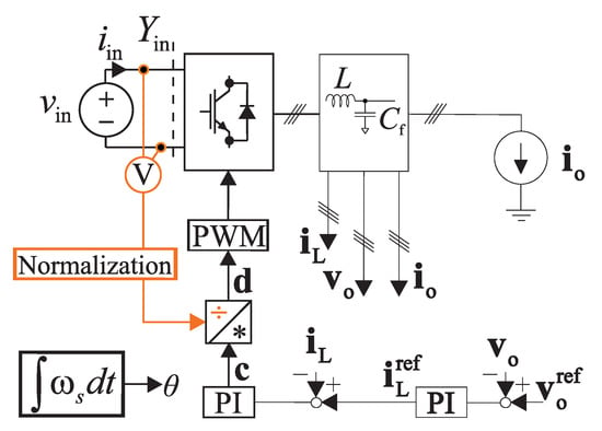
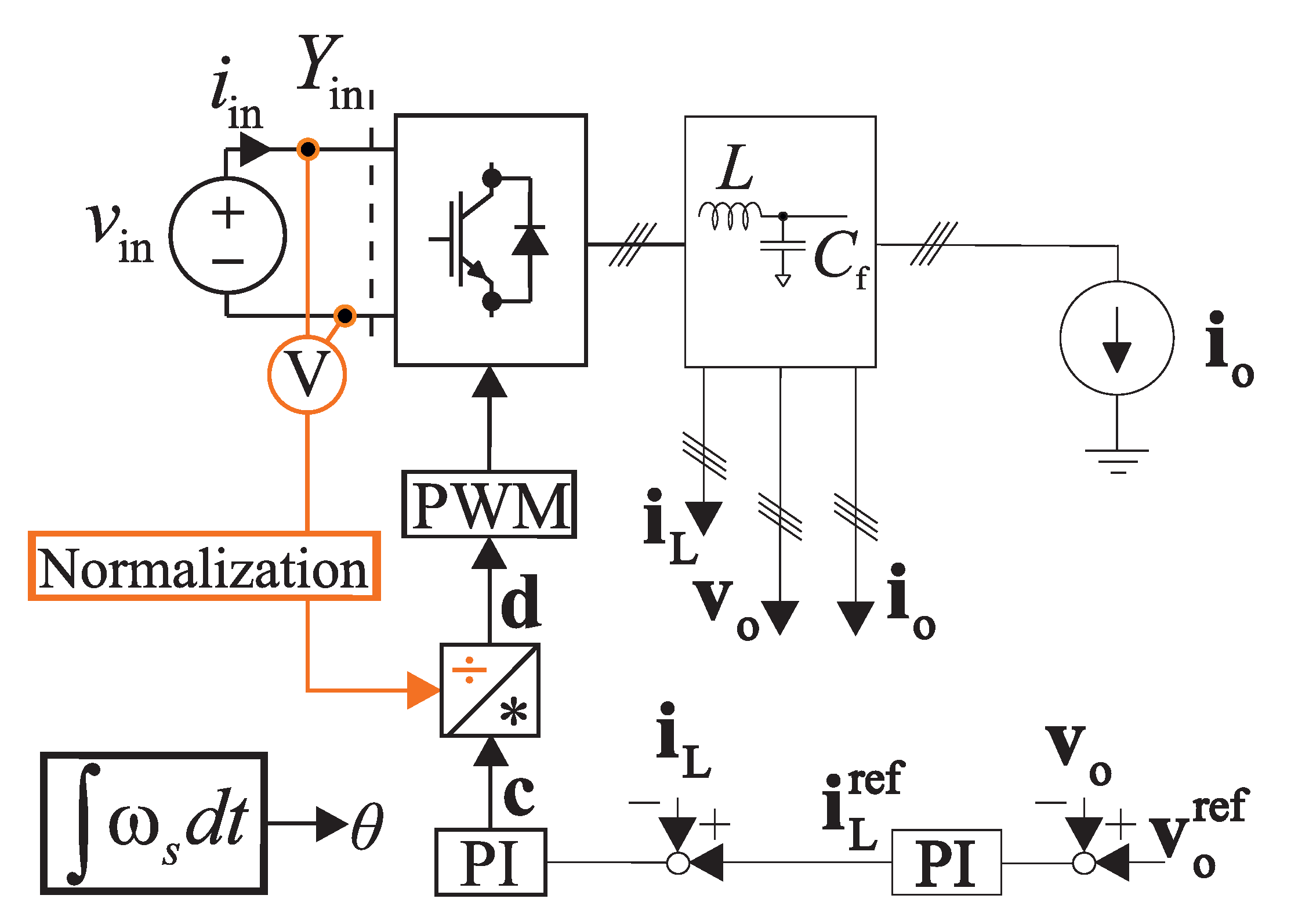
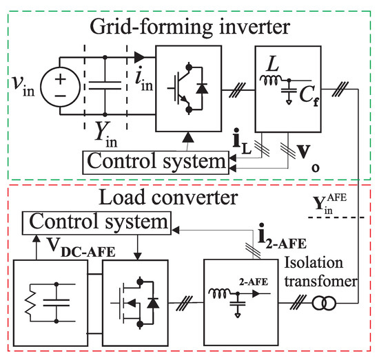
Figure 1 shows a simplified block diagram of a grid-forming inverter. The traditional cascaded inductor current and output voltage feedback are implemented on the AC side. In the unterminated model, the load is an ideal current sink and the power is fed from a DC voltage source. The deviations in the DC voltage are compensated by dividing the inverter control signal with the normalized DC voltage. The DC voltage is normalized because in the nominal condition without the feedforward the current controllers output, , equals the duty ratio . Bold notation denotes a vector that consists of direct and quadrature components. If the vector notation is not used, subscripts “d” and “q” are used to denote the direct and quadrature components, respectively. This normalization would not be required if the dynamics were modeled with a PWM reference voltage instead of the duty ratio.
Figure 1.
Simplified block diagram of the analyzed converter.
The open-loop transfer-function presentation from the system inputs to the system outputs can be given as [10]:
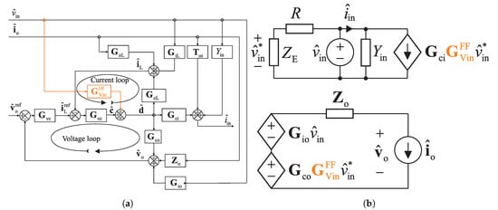
where , , and denote the input admittance, the input-to-inductor current transfer matrix, and the input-to-output transfer matrix, respectively. , , and stand for the output-to-input transfer matrix, the output-to-inductor current transfer matrix, and the output impedance matrix, respectively. The control-related transfer matrices , and denote the control-to-input current, the control-to-inductor current, and the control-to-output voltage transfer matrices, respectively. The open-loop transfer-function matrices are used in Figure 2a with the addition of the current controller and the voltage controller transfer matrices to form the closed-loop system. The system parameters and operating point values are given in Table 1 where the synchronous-reference-frame-steady-state values are defined as peak values. The abbreviation ESR stands for the equivalent series resistance. The input-voltage feedforward is modeled by .
Figure 2.
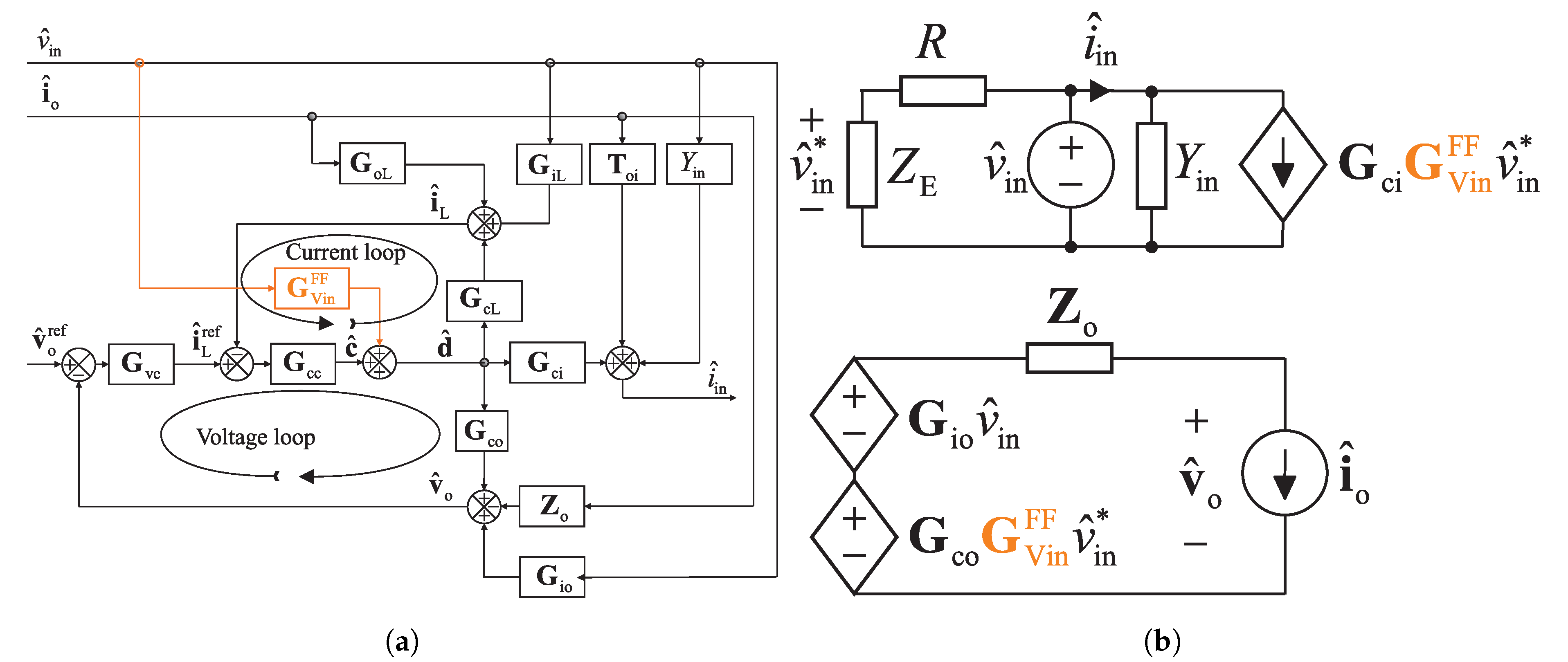
(a) Control block diagram of the inverter system. (b) Circuit diagram of the input and the output dynamics with the feedforward.
Table 1.
Parameters and operating point values.
The division by the input-voltage feeforward is highlighted in orange in Figure 2a. Figure 2b shows the input and the output dynamics of the system with additional elements R and that will be used to analyze the effect of a low-pass filter in Section 5. In Section 2 and Section 3, is made open, and therefore, equals . The dynamic presentation for the input-voltage feedforward is derived by two methods in the next section.
3. Input-Voltage Feedforward and Input-to-Output Dynamics
This section considers the inverter input-to-output dynamics with the feedforward. First, a transfer matrix from the input voltage to the duty ratios is derived. Then, the detrimental effect of the delay with the input-voltage feedforward is examined.
3.1. Linearization Approach
The dynamics of the input-voltage feedforward can be solved by linearizing the division of the current controller output d and q components, and , by the input voltage with respect to the input voltage :
where , , and are the steady-state values of the input voltage and duty-ratio d and q components, respectively. The hat is used to denote small-signal values. The results can be collected to a transfer matrix
which presents how affects and . The input-voltage-feed-forward-affected input-to-output dynamics are calculated according to Figure 2b:
3.2. Mitigating the Effect of Input-Voltage Deviations
In the ideal case, the feedforward would reduce the gain of the input-voltage-to-output voltage dynamics to zero. Therefore, the gain of the feed-forward-affected input-to-output dynamics should be zero:
The ideal feedforward gain can be given as follows
In a synchronous-switching buck-type converter, the transfer functions from the input voltage and the duty-ratio to the output have the dynamics of the filter, and the dynamics differ only at the DC gain if the voltage drop over the components is assumed small. Therefore, the following analysis can be done by using the DC gains. The cross-coupling gains of the control-to-output transfer function are approximated to be very small:
The resulting ideal input-voltage feed-forward transfer function is the same as the previous linearization (4) result of the input voltage division:
3.3. Effect of the Delay
In the previous analysis, the delay from the digital control system was neglected. Now the delay is modeled by a third-order Padé approximation [4]:
where is the delay length in seconds, and is the switching cycle, . The delay matrix that is used with the multivariable control-related transfer matrices is defined as follows
The input-feedforward affected input-to-output dynamics with the delay is given by
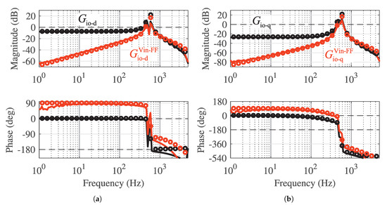
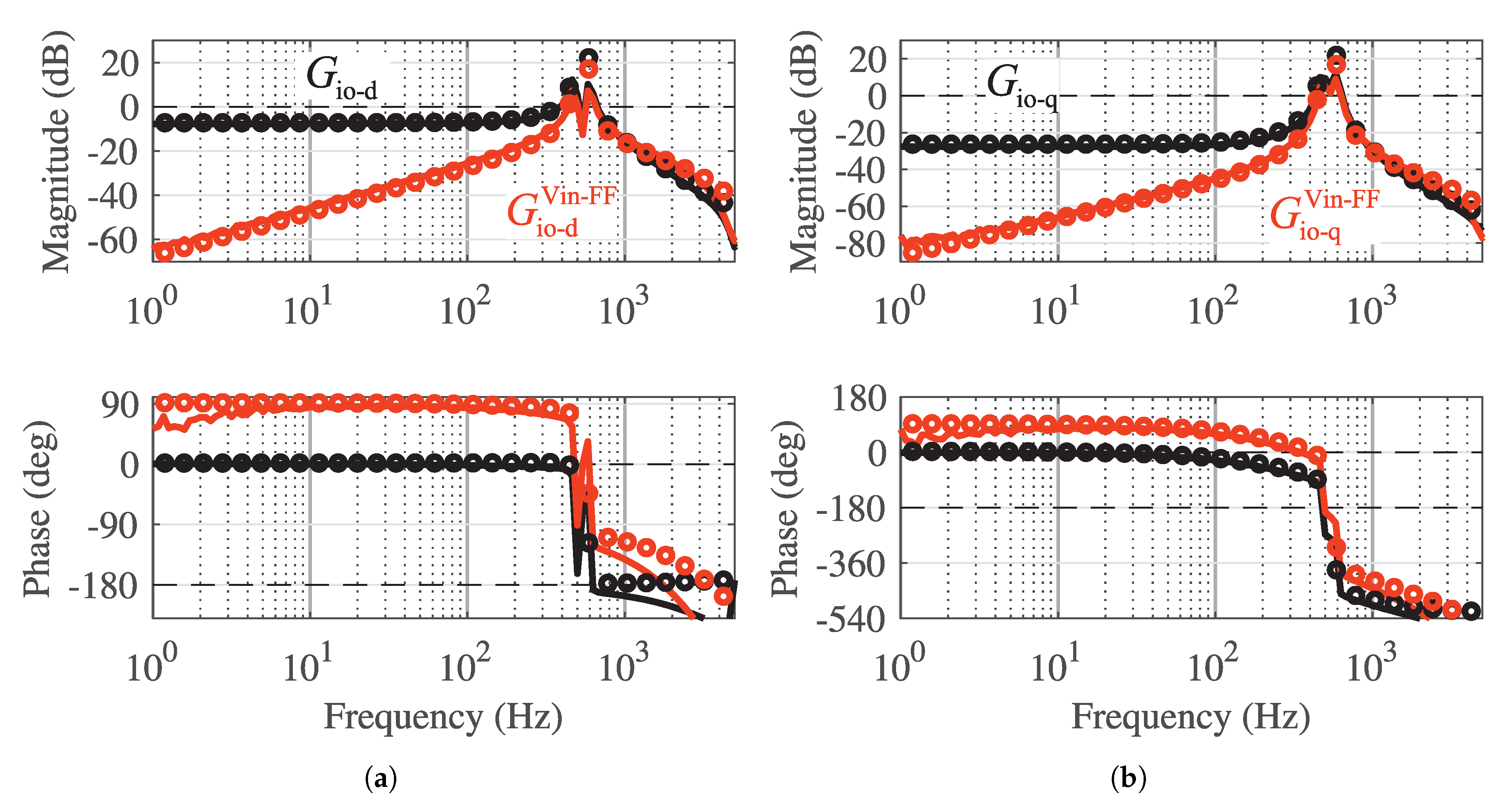
Figure 3a,b show the frequency responses of the input-to-output dynamics without the feedforward and with the feedforward using the model in (13). The input-voltage feedforward clearly reduces the gain of the input-to-output dynamics both in the d and q components at low frequencies. However, due to the phase shift caused by the delay, the effect of the feedforward becomes detrimental at 1111 Hz because the magnitude is higher with the feedforward than without it. In addition to the modeled frequency responses, Figure 3 shows a verification from a real-time hardware-in-the-loop (HIL) simulation that was performed on Typhoon HIL model 402.
Figure 3.
Modeled (dots) and HIL simulation (line) open-loop input-to-output dynamics (a) d component and (b) q component.
The frequency where the feedforward becomes detrimental can be solved by finding the phase shift in the feedforward signal that causes the absolute values of the input-to-output dynamics with and without the feedforward to equal:
where, is used to model the phase shift at the angle by its real and imaginary parts according to the Euler’s formula. The aforementioned similarity in the input-to-output dynamics and the control-to-output dynamics is used to simplify the analysis. The transfer functions are approximated by their DC gains:
where can be solved as:
The delay causes a negative phase shift, and the smallest negative phase shift required is −60°. The frequency where the phase shift takes place is
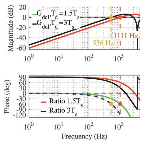
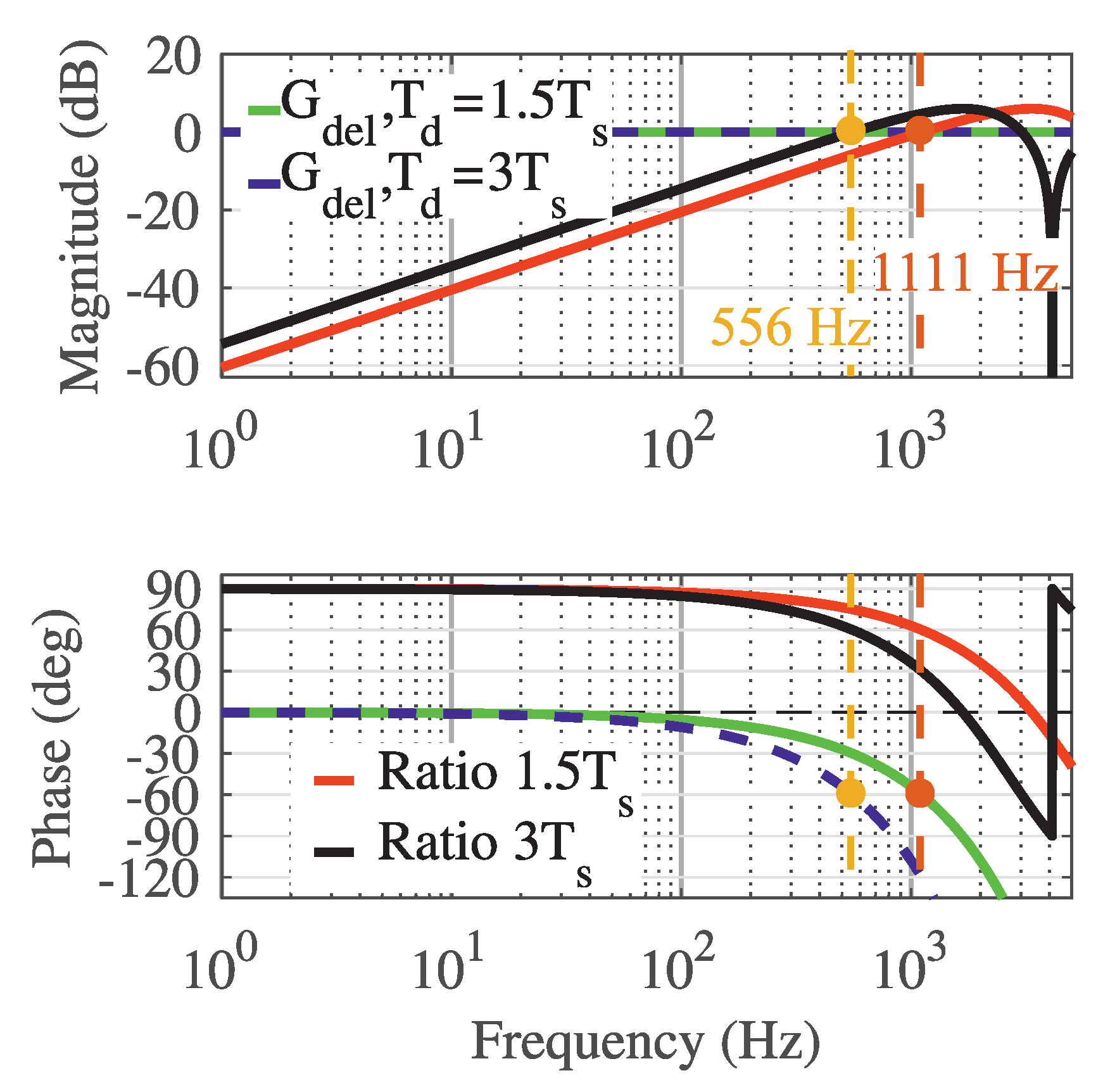
where k denotes the ratio between the delay and the switching cycle . If equals 1.5 , the frequency is 1111 Hz. Figure 4 shows the ratio of and with the delays of 1.5 and 3 and the analytically solved frequencies for the corresponding delay lengths. As the figure shows, (18) gives correctly the frequency where the input-to-output transfer function has a equal magnitude with the feedforward and without it and the the delay phase shift is . These findings highlight the fact that, due to the delay, the feedforward provides no perfect decoupling from the input-voltage deviations, and the delay must be modeled. In Section 5, a first-order low-pass filter is used to mitigate the delay effect.
Figure 4.
The ratios of and the Padé approximations of the delay with the delay length of 1.5 and 3.
4. Input Admittance
This section examines the input admittance with the feedforward. First, the ideal input admittance that is a special parameter known from the modeling of DC-DC converters is derived. Then, the input admittance is analyzed with the inductor-current feedback and the output-voltage feedback.
4.1. Ideal Input Admittance
The ideal input admittance has been applied in modeling the source effect on the control-to-output dynamics in DC-DC converters [13,21,22,23] and the ideal-input-admittance components in three-phase inverters [24]. From the modeling of DC-DC converters [13], it is known that with the input-voltage feedforward the input admittance corresponds to the ideal input admittance. The ideal input admittance is a special parameter that corresponds to a formulation (null-double-injection admittance) [22] from the extra element theorem [25]. Next, the ideal input admittance is derived similarly for the three-phase voltage-source inverter (VSI) as for DC-DC converters [13,23]. The ideal input admittance for the three-phase VSI can be given as
where the inverse of implies that the ideal input admittance corresponds to a case where the output-voltage controller is infinitely fast. In order to simplify the analysis, the resistive losses and the cross coupling between the d and q channels are neglected. The transfer functions of (19) can be approximated as follows
The ideal input admittance (19) can be shown to be:
The result is in line with the ideal input admittance of DC-DC converters [13,23]. Despite the approximations, the model is adequate as it will be shown in Section 4.2.
4.2. Closed-Loop Input Admittance with the Input-Voltage Feedforward
The inductor-current feedback and the output-voltage feedback are formed according to Figure 2a. The delay is neglected in the following approximation. However, when the approximation is not used and the delay is modeled, each of the control-related transfer matrices , and are multiplied from right by given in (12). The multi-variable inductor-current control-loop gain is given by
For simplicity, only the closed-loop input admittance is studied among the transfer functions. At first, the inductor-current control loop is closed
where the superscript denotes that the secondary feedback loop is closed. The equation can be manipulated to a form that resembles the asymptotic-gain model. First, (26) is multiplied on the both sides from left by
Rearranging the terms, the expression for can be found. Then both sides are multiplied from left by resulting:
where it is assumed that the magnitude of the multivariate loop-gain (25) is very high. Equation (28) shows that . The same analysis can be done for the output-voltage feedback
With the input-voltage feedforward, the input admittance remains unchanged although the inductor current and output voltage feedback loops are closed, and it corresponds to the ideal input admittance defined in (24).
Figure 5a shows the open-loop input admittance with and without the feedforward. The feedforward clearly increases the input admittance to . However, due to the delay in the sampling and digital control, the phase drops and the gain changes at high frequencies. When the current and the output-voltage control loops are closed, the input impedance appears as a constant power load within the control bandwidth as Figure 5b shows. Nevertheless, the input-voltage feedforward keeps the admittance in even outside the voltage controller-bandwidth. With the feedforward, the region where the phase is −180° is wider than without the feedforward. The phase above −90° can cause impedance-based stability issues at the DC interface of the converter.
Figure 5.
(a) Open-loop input admittance with and without the input voltage feedforward. (b) Closed-loop input admittance with and without the input voltage feedforward.
5. Bandwidth Considerations
As it can be seen from the frequency responses in Figure 3a,b, and Figure 4, the feedforward does not minimize the gain of the input-to-output dynamics at all frequencies due to the delay. Instead, the gain is increased at frequencies higher than .
A high frequency stability problem between a HVDC Converter and AC grid due to the AC output-voltage feedforward was reported in [26]. The problem was solved by implementing a low-pass filter in the feedforward. Consequently, implementing a low-pass filter in the input-voltage feedforward to reduce the high frequency gain is analyzed. The negative effect of the feedback is studied by inspecting the ratio of the input-to-output dynamics with and without the feedforward.
The extra-element method given in [25,27] is a technique to facilitate modeling of systems consisting of linear transfer functions, and the theorem has been used, for example, in tuning an active filter in a wind-power-plant system [28]. In the present paper, the extra element theorem can be used to give a formulation for the system in Figure 2b where adding the extra element implements a low-pass-filtered input-voltage feedforward:
where is the transfer function from the input voltage to the output voltage when the the extra element, , is made a short. is the analyzed transfer function with the influence of . The single-injection driving point impedance, , is the impedance seen from the extra element when the input voltage is replaced by a short. The null-double injection impedance, , is the impedance seen from the extra element when the input voltage nulls the effect of the measurement from the extra element on the output voltage.
The low-pass filter is modeled by impedances R and . R is a resistor. is the reactance of a capacitor
where is the angular frequency and C the extra-element capacitor capacitance. When is short-circuited, equals and there is no low-pass filter as Figure 2b shows. By changing the capacitor values, the cut-off frequency of the RC-low-pass filter can be changed. The impedances are only used as a tool to model the cut-off frequency of a digital low-pass filter, and therefore, R is set to 1 .
The ratio describing how the extra element affects the system dynamics can be given as follows:
can be solved as a function of desired K by manipulating (35) to the second-order equation form that is easy to solve:
The equation has two solutions, and . The required cut-off frequency, , for the low-pass filter is given by
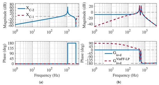
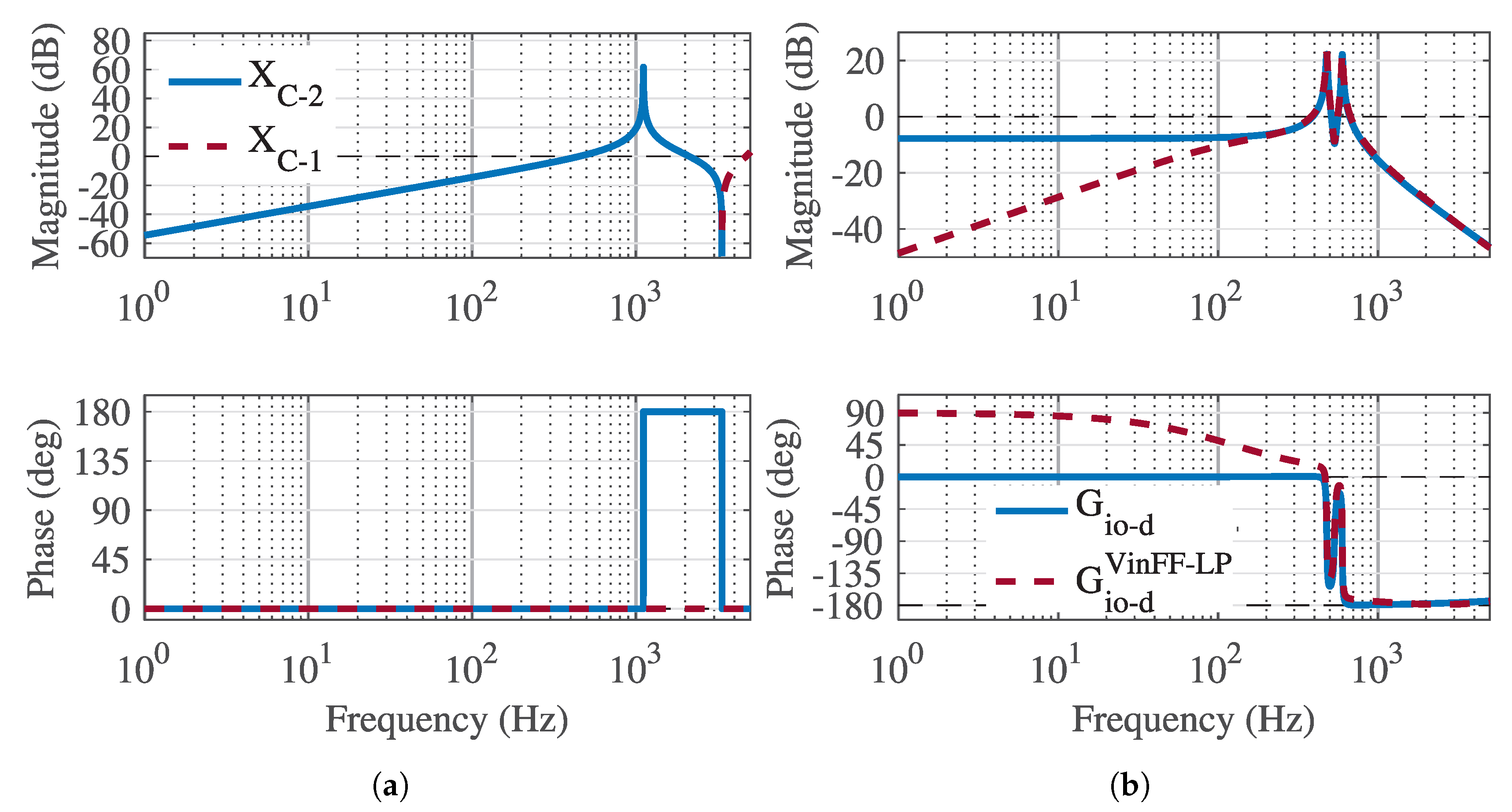
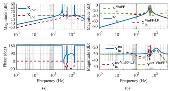
Figure 6a shows the solutions to (36) as bode plots. Only real-solutions, where the phase is 0°, can be implemented. In Figure 6a, is zero below 3360 Hz which implies that design criterion is met only when the feedforward is not used. Between 1111 Hz and 3360 Hz, the phase of solution is −180° which means that the low-pass filter should have a right-half-plane pole that obviously cannot be implemented. This result implies that a first-order low-pass filter cannot be used to mitigate the detrimental effect from the delay in the frequency range between 1111 Hz and 3360 Hz. However, solution can be implemented on frequencies below 1111 Hz.
Figure 6.
(a) Solutions XC−1 and XC−2 for the low-pass filter related to the input-to-output dynamics. (b) Input-voltage feedforward-affected input-to-output dynamics d component with and without the low-pass filter.
A low-pass filter is implemented so that the magnitude with and without the feedforward is the same at 250 Hz. The required cut-off frequency is calculated at 250 Hz from shown in Figure 6a. The required cut-off frequency is 123.5 Hz. Figure 6b shows and the low-pass-filtered input-voltage-feedforward affected input-to-output dynamics d component, . As it can be seen, the transfer functions have the same gain at 250 Hz. However, this may not be advantageous because the effect of the feedforward is highly reduced at the low frequencies.
More benefits could be achieved from the input admittance point of view. In order to analyze the effect of the low-pass filter on the input admittance, the elements and are redefined:
As an example we can assume that the input admittance should be only 3 dB higher with the feedforward than without the feedforward at 200 Hz. The solution can be seen in Figure 7a, which shows that is realizable at 200 Hz and it corresponds to a low-pass filter with a cut-off frequency of 37.4 Hz. The upper gain figure in Figure 7b shows the comparison of the models of the input admittance , the input admittance with the feedforward , and the input admittance with the low-pass-filtered feedforward in the open loop. The gain difference at 200 Hz is exactly 3 dB. However, the lower figure in Figure 7b shows that the difference is 2 dB, which is due to the current and the voltage controllers.
Figure 7.
(a) Solutions XC−1 and XC−2 for the low-pass filter related to the input admittance. (b) Upper figure: comparison of the open-loop input admittance gain and lower figure: comparison of the closed-loop input admittance gain.
The benefit from the low-pass filter in the closed-loop input admittance is clearly visible. However, as it is shown in Figure 6b, the feedforward effect on the input-to-output dynamics is highly reduced by a low-pass filter. In the next section, it will be shown that the DC link capacitor can increase the input admittance significantly, and the feedforward effect on the input admittance could become negligible.
6. Experimental Verification
Figure 8 shows the setup of the system under study. The grid-forming inverter whose input-related dynamics are inspected is loaded by an active rectifier. The current is controlled to make the load converter behave as a current sink. On the DC side, the voltage over a resistive load, , is controlled. However, during the frequency-response measurements at low frequencies, the DC-voltage controller was not used. The switching frequency used in the load converter is 20 kHz. The control system of the load converter was implemented by dSpace and the grid-forming inverter was controlled by a Imperix Boombox. The parameters of the grid-forming inverter are given in Table 2. The voltage controller has the same PI-controller as in the analysis given in Section 2, Section 3, Section 4 and Section 5. However, an additional low-pass filter is implemented at 500 Hz; therefore, the voltage controller is given by
Figure 8.
Block diagram of the laboratory setup.
Table 2.
Experimental grid-forming inverter parameters and operating point values.
In the experiments, the load converter is not an ideal current sink. Hence, there is an impedance-based interaction, and the load effect from the active rectifier must be considered [10,24]:
where is the AC input-admittance of the active rectifier, and the active rectifier is modeled by similar principles that have been used to model grid-connected PV inverters [4]. The superscript “L” is used to denote load-affected dynamics (the superscript is omitted in Figure 9 for simplicity).
Figure 9.
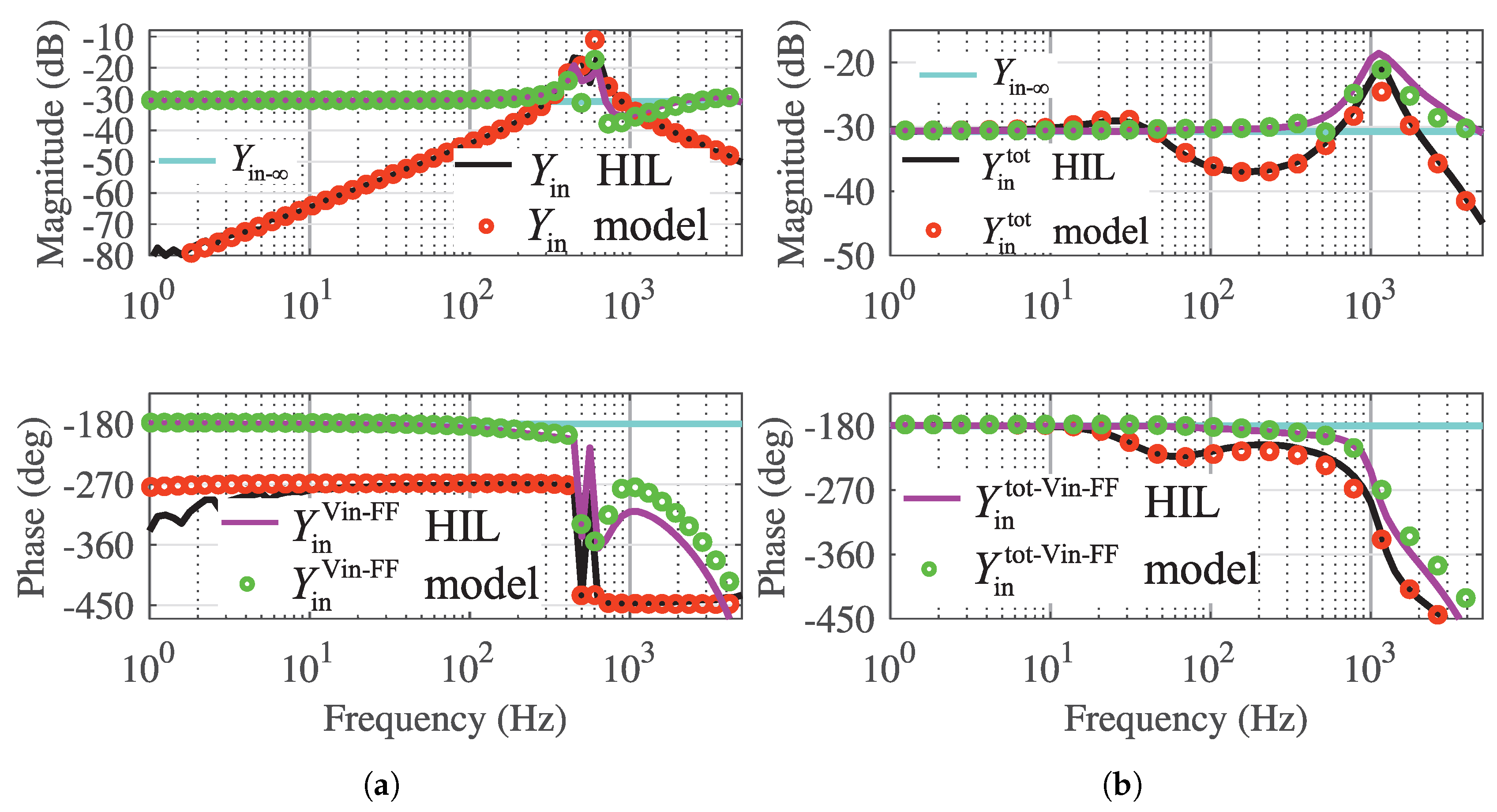
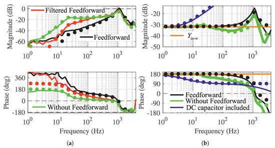
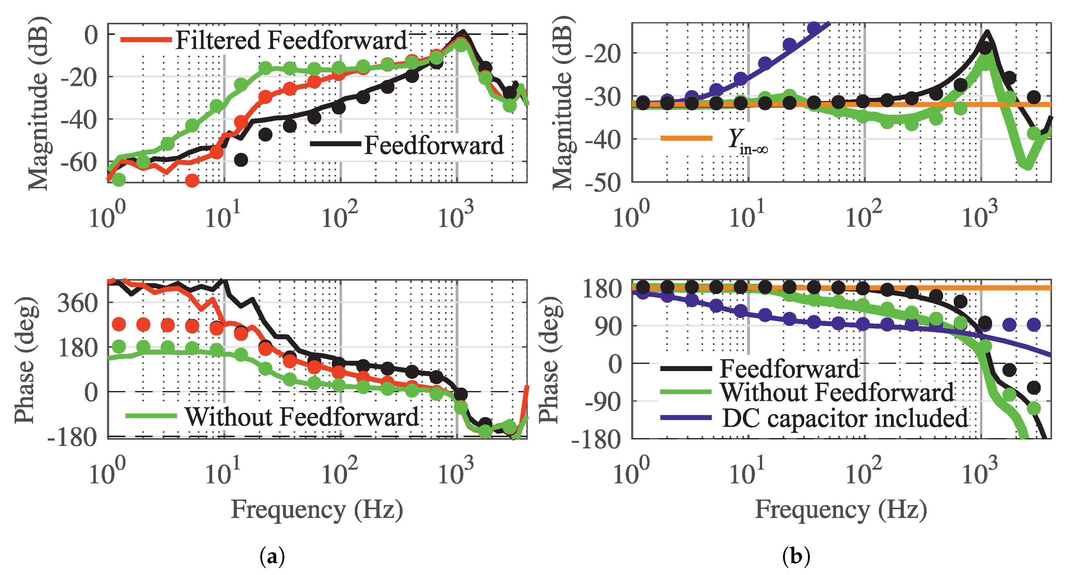
(a) Modeled (dots) and experimental (line) closed-loop input-to-output dynamics d component. (b) Modeled (dots) and experimental (line) closed-loop input admittance.
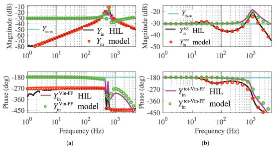
Figure 9a,b show the measured frequency responses related to the closed-loop input-to-output dynamics and input admittance, respectively. The load-affected model clearly models well the input-to-output dynamics and the input admittance. The effect of the input-voltage feedforward is clearly visible in the closed-loop input-to-output dynamics d component, . The low-pass filter has only a minor effect on the high-frequency magnitude in . Therefore, the low-pass filter is not a good solution to reduce the detrimental effect in high frequencies. If the DC-capacitance, that is commonly used in the DC link, is included with the input admittance, the gain increases significantly at low frequencies so that the input-voltage feedforward makes no significant difference with the used DC capacitor size.
7. Analysis of the Proposed Model
This section compares the proposed ideal input admittance to existing ideal input admittance elements. It is shown that the existing model can be extracted from the proposed model.
Recently, a transfer-matrix representation for an ideal input admittance has been given [24] as:
The model in [24] is used as a tool to analyze the source-affected control-to-output dynamics of a three-phase grid-forming inverter in the DQ domain. In the present paper, the proposed ideal input admittance (19) is a scalar function that can be measured from a real system when the input-voltage feedforward is used. The presentation in (19) can be used to form the elements in in [24]. The key to solving the elements is to choose corresponding elements from the transfer matrices in (19) before any mathematical operations including the inverse of :
where m and n are the elements of the matrices and vectors.
8. Conclusions
The input-voltage feedforward control is widely used in power-electronic converters to prevent deviations in the DC input voltage appearing in the converter output. However, the feedforward implementation in three-phase converters has not been modeled in detail. This paper has proposed a dynamic of a three-phase grid-forming inverter utilizing the input-voltage feedforward.
The model accurately represents the feedforward-affected input admittance and the input-voltage-to-output-voltage dynamics. The gain in the input-voltage-to-output-voltage dynamics is significantly reduced by the feedforward. However, our study shows in detail that the feedforward does not provide an ideal decoupling from the input-voltage deviations due to the delay. The delay causes a detrimental effect at high frequencies, and the study shows that a minor improvement can be achieved by low-pass filtering the feedforward control signal.
The input admittance is affected detrimentally by the feedforward. This paper has demonstrated that the unterminated input admittance can be approximated well by the ideal input admittance which corresponds to an inverter with an infinite fast output-voltage controller. However, if the DC capacitor is considered as a part of the admittance, the input admittance shape could be dictated by the capacitor admittance.
The proposed model can be applied to the impedance-based stability analysis at the DC interface of three-phase inverters and to analyze the effect of the deviations in the DC voltage to the AC voltage.
Author Contributions
Conceptualization, M.B.; Formal analysis, M.B.; Investigation, M.B.; Supervision, T.R.; Validation, M.B.; Writing—original draft, M.B.; Writing—review & editing, T.R. All authors have read and agreed to the published version of the manuscript.
Funding
This research received external funding from Business Finland project SolarX.
Conflicts of Interest
The authors declare no conflicts of interest.
References
- Yang, D.; Wang, X. Unified modular state-space modeling of grid-connected voltage-source converters. IEEE Trans. Power Electron. 2020, 35, 9702–9717. [Google Scholar] [CrossRef] [Scilit]
- Wen, B.; Boroyevich, D.; Burgos, R.; Mattavelli, P.; Shen, Z. Small-signal stability analysis of three-phase AC systems in the presence of constant power loads based on measured d-q frame impedances. IEEE Trans. Power Electron. 2015, 30, 5952–5963. [Google Scholar] [CrossRef] [Scilit]
- Lu, D.; Wang, X.; Blaabjerg, F. Impedance-based analysis of DC-link voltage dynamics in voltage-source converters. IEEE Trans. Power Electron. 2019, 34, 3973–3985. [Google Scholar] [CrossRef] [Scilit]
- Aapro, A.; Messo, T.; Roinila, T.; Suntio, T. Effect of active damping on output impedance of three-phase grid-connected converter. IEEE Trans. Ind. Electron. 2017, 64, 7532–7541. [Google Scholar] [CrossRef] [Scilit]
- Unamuno, E.; Rygg, A.; Amin, M.; Molinas, M.; Barrena, J.A. Impedance-based stability evaluation of virtual synchronous machine implementations in converter controllers. In Proceedings of the 2018 International Power Electronics Conference (IPEC-Niigata 2018 -ECCE Asia), Niigata, Japan, 20–24 May 2018; IEEE: Piscataway, NJ, USA, 2018; pp. 759–766. [Google Scholar]
- Xue, D.; Liu, J.; Liu, Z.; Tu, Y.; Liu, T. Modeling and analysis of DC terminal impedance of voltage-source converters with different control modes. IEEE Trans. Power Electron. 2020, 35, 5883–5896. [Google Scholar] [CrossRef] [Scilit]
- Moradi-Shahrbabak, Z.; Tabesh, A. Effects of front-end converter and DC-link of a utility-scale PV energy system on dynamic stability of a power system. IEEE Trans. Ind. Electron. 2018, 65, 403–411. [Google Scholar] [CrossRef] [Scilit]
- Wang, R.; Wu, Y.; He, G.; Lv, Y.; Du, J.; Li, Y. Impedance modeling and stability analysis for cascade system of three-phase PWM rectifier and LLC resonant converter. Energies 2018, 11, 3050. [Google Scholar] [CrossRef] [Scilit]
- Radwan, A.A.A.; Mohamed, Y.A.R.I.; El-Saadany, E.F. Assessment and performance evaluation of DC-side interactions of voltage-source inverters interfacing renewable energy systems. Sustain. Energy Grids Netw. 2015, 1, 28–44. [Google Scholar] [CrossRef] [Scilit]
- Berg, M.; Messo, T.; Suntio, T. Frequency response analysis of load effect on dynamics of grid-forming inverter. In Proceedings of the 2018 International Power Electronics Conference (IPEC-Niigata 2018 -ECCE Asia), Niigata, Japan, 20–24 May 2018; pp. 963–970. [Google Scholar]
- Bogdanov, D.; Ralchev, M.; Mateev, V.; Marinova, I. Harmonic spectrum filtration for current sensor measurements. In Proceedings of the 2019 16th Conference on Electrical Machines, Drives and Power Systems (ELMA), Varna, Bulgaria, 6–8 June 2019. [Google Scholar]
- Karppanen, M.; Sippola, M.; Suntio, T. Dynamics of input-voltage-feedforward-controlled buck converter. In Proceedings of the INTELEC 06-Twenty-Eighth International Telecommunications Energy Conference, Providence, RI, USA, 10–14 September 2006; IEEE: Piscataway, NJ, USA, 2006; pp. 1005–1013. [Google Scholar]
- Karppanen, M.; Suntio, T.; Sippola, M. Dynamical characterization of input-voltage-feedforward-controlled buck converter. IEEE Trans. Ind. Electron. 2007, 54, 1005–1013. [Google Scholar] [CrossRef]
- Jia, P.; Zheng, T.Q.; Li, Y. Research on input-voltage feedforward control for high-order converter topologies. IET Power Electron. 2014, 7, 2778–2790. [Google Scholar]
- Ramezani, M.; Li, S.; Golestan, S. Analysis and controller design for stand-alone VSIs in synchronous reference frame. IET Power Electron. 2017, 10, 1003–1012. [Google Scholar] [CrossRef] [Scilit]
- Han, Y.; Shen, P.; Zhao, X.; Guerrero, J.M. Control strategies for islanded microgrid using enhanced hierarchical control structure with multiple current-loop damping schemes. IEEE Trans. Smart Grid 2017, 8, 1139–1153. [Google Scholar] [CrossRef] [Scilit]
- Suul, J.A.; D’Arco, S.; Rodríguez, P.; Molinas, M. Impedance-compensated grid synchronisation for extending the stability range of weak grids with voltage source converters. IET Gener. Transm. Distrib. 2016, 10, 1315–1326. [Google Scholar] [CrossRef] [Scilit]
- D’Arco, S.; Suul, J.A.; Fosso, O.B. A virtual synchronous machine implementation for distributed control of power converters in smartgrids. Electr. Power Syst. Res. 2015, 122, 180–197. [Google Scholar] [CrossRef] [Scilit]
- Mo, O.; Darco, S.; Suul, J.A. Evaluation of virtual synchronous machines with dynamic or quasi-stationary machine models. IEEE Trans. Ind. Electron. 2017, 64, 5952–5962. [Google Scholar] [CrossRef] [Scilit]
- Kroutikova, N.; Hernandez-Aramburo, C.; Green, T. State-space model of grid-connected inverters under current control mode. IET Electr. Power Appl. 2007, 1, 329. [Google Scholar] [CrossRef] [Scilit]
- Vesti, S.; Suntio, T.; Oliver, J.A.; Prieto, R.; Cobos, J.A. Effect of control method on impedance-based interactions in a buck converter. IEEE Trans. Power Electron. 2013, 28, 5311–5322. [Google Scholar] [CrossRef] [Scilit]
- Suntio, T. Dynamic Profile of Switched-Mode Converter: Modeling, Analysis and Control; Wiley-VCH: Weinheim, Germany, 2009. [Google Scholar]
- Suntio, T.; Messo, T.; Puukko, J. Power Electronic Converters: Dynamics and Control in Conventional and Renewable Energy Applications; Wiley-VCH: Weinheim, Germany, 2017. [Google Scholar]
- Suntio, T.; Messo, T.; Berg, M.; Alenius, H.; Reinikka, T.; Luhtala, R.; Zenger, K. Impedance-based interactions in grid-tied three-phase inverters in renewable energy applications. Energies 2019, 12, 464. [Google Scholar] [CrossRef] [Scilit]
- Middlebrook, R. Null double injection and the extra element theorem. IEEE Trans. Educ. 1989, 32, 167–180. [Google Scholar] [CrossRef] [Scilit]
- Zou, C.; Rao, H.; Xu, S.; Li, Y.; Li, W.; Chen, J.; Zhao, X.; Yang, Y.; Lei, B. Analysis of resonance between a VSC-HVDC converter and the AC grid. IEEE Trans. Power Electron. 2018, 33, 10157–10168. [Google Scholar] [CrossRef] [Scilit]
- Middlebrook, R.D. The N Extra Element Theorem. IEEE Trans. Circuits Syst. I Fundam. Theory Appl. 1998, 45, 919–935. [Google Scholar] [CrossRef] [Scilit]
- Guest, E.; Jensen, K.H.; Rasmussen, T.W. Mitigation of harmonic voltage amplification in offshore wind power plants by wind turbines with embedded active filters. IEEE Trans. Sustain. Energy 2020, 11, 785–794. [Google Scholar] [CrossRef] [Scilit]

© 2020 by the authors. Licensee MDPI, Basel, Switzerland. This article is an open access article distributed under the terms and conditions of the Creative Commons Attribution (CC BY) license (http://creativecommons.org/licenses/by/4.0/).