Fault Ride-Through Power Electronic Topologies for Hybrid Energy Storage Systems †


1
LEMUR Research Group, Deprtment of Electrical, Electronic, Computers and Systems Engineering, University of Oviedo, 33204 Gijon, Spain
2
PEMC Research Group, Deprtment of Electrical and Electronic Engineering, University of Nottingham, Nottingham NG7 2RD, UK
*
Author to whom correspondence should be addressed.
†
This paper is an extended version of our paper published in 2016 IEEE Energy Conversion Congress and Exposition (ECCE), Milwaukee, WI, USA, 18–22 September 2016; pp. 1–8.
Energies 2020, 13(1), 257; https://doi.org/10.3390/en13010257
Submission received: 4 December 2019
/
Revised: 29 December 2019
/
Accepted: 1 January 2020
/
Published: 4 January 2020
(This article belongs to the Special Issue Analysis and Design of Hybrid Energy Storage Systems)
Abstract
:This work presents a fault ride-through control scheme for a non-isolated power topology used in a hybrid energy storage system designed for DC microgrids. The hybrid system is formed by a lithium-ion battery bank and a supercapacitor module, both coordinated to achieve a high-energy and high-power combined storage system. This hybrid system is connected to a DC bus that manages the power flow of the microgrid. The power topology under consideration is based on the buck-boost bidirectional converter, and it is controlled through a bespoke modulation scheme to obtain low losses at nominal operation. The operation of the proposed control scheme during a DC bus short-circuit failure is shown, as well as a modification to the standard control to achieve fault ride-through capability once the fault is over. The proposed control provides a protection to the energy storage systems and the converter itself during the DC bus short-circuit fault. The operation of the converter is developed theoretically, and it has been verified through both simulations and experimental validation on a built prototype.
1. Introduction
Power quality is a major concern in modern power systems, particularly in weak microgrids. The concern for the economic importance of power quality issues has led to the development of standards and regulations that define the requirements for equipment and utilities in grid applications [1,2].
Faults in power systems are one of the major causes of power quality issues. Depending on the proximity to the system under consideration, the effects vary substantially. From variations in the voltage and current waveforms parameters (amplitude, frequency and phase) to voltage sags and, in extreme cases, even to voltage outages. Therefore, a continuous research is being done in turning the electric system and its components to fault-tolerant, to boost and develop a more resilient electric grid [3].
In particular, the effects of voltage issues in microgrids have attracted a lot of attention from the research community. One particular case is when the Point of Common Coupling (PCC) is implemented though a Power Electronic Converter (PEC), which interfaces the AC grid with a DC bus. From this DC bus, the microgrid can be supplied in AC, DC or hybrid AC/DC lines [4]. However, the control of the DC bus voltage at the DC side of the grid interfacing converter is critical to ensure adequate operation of the system [5]. In an increasing number of applications, Energy Storage Systems (ESSs) are connected to this DC bus through dedicated PECs, aiming to primarily provide the needed energy in case the microgrid operates in islanding mode. Additionally, the ESS balances the energy flows of the microgrid, accounting for stochastic behavior of distributed generation and loads, therefore decreasing this random factor in the power consumed from the grid [5]. In any case, the sizing of the accumulator is carried out considering energy requirements [6].
Upon changes in the microgrid power flows (due variable load profiles or injection of power from distributed generators), or even voltage variations in the grid, imply transient fluctuations in the DC bus. Usually, the ESSs used for energy supply in microgrids present limited dynamics, and the large transient power spikes reduce their operating lifetime (e.g., in electrochemical batteries) [6]. In these cases, a fast, high-power capability storage system (e.g., Supercapacitor Module (SM)) can be included, forming a Hybrid Energy Storage System (HESS) [6,7,8]. With an adequate coordinated control, these hybrid systems ensure a stiff behavior of the DC bus, decoupling the grid and the microgrid sides. However, also, they enhance the system reliability by preventing the low-dynamic storage systems to provide large current spikes, resulting in an increase of the system lifetime [9]. HESSs are gaining increased research interest due to their potential benefits in power and energy support in grid applications [5].
Fault-tolerant HESSs are intended to provide these capabilities but at the same time being able to deal with fault conditions in the grid. Depending on the magnitude and the distance to the fault location, the induced variations on the DC bus might vary substantially [4]. For faults far away from the PCC, at distribution or even at transmission levels, the effects within the microgrid are generally limited to voltage sags that can be solved by the regular operation of the HESS. However, for faults at distribution level, closer to the PCC, or even at the DC bus inside the microgrid, more severe voltage variations, and even short-circuit currents might appear through the storage subsystem [4]. Fault-tolerant topologies prevent these dangerous short-circuit currents to circulate across the storage subsystem [10]. In addition, fault ride-through is also expected in this case, therefore once the fault is removed, the system is able to automatically operate properly again in a reasonable amount of time, in accordance to the standards/regulations and the expected behavior of the microgrid [4].
Usually, fault-tolerant topologies make use of additional series switches that interrupt the current flow if a short-circuit appears at the DC bus [4]. In addition to the increase of the system cost, larger losses appear in regular operation due these series switches. This work proposes a non-isolated topology for a fault-tolerant hybrid storage system with fault ride-through capability, suitable for low to medium power applications in microgrids. Its operation is described, and a commutation scheme is proposed to keep the losses in the range of a simple, non-fault-tolerant solution. The performance of the system is validated through both simulations and experimental results on a working prototype of 10 kW.
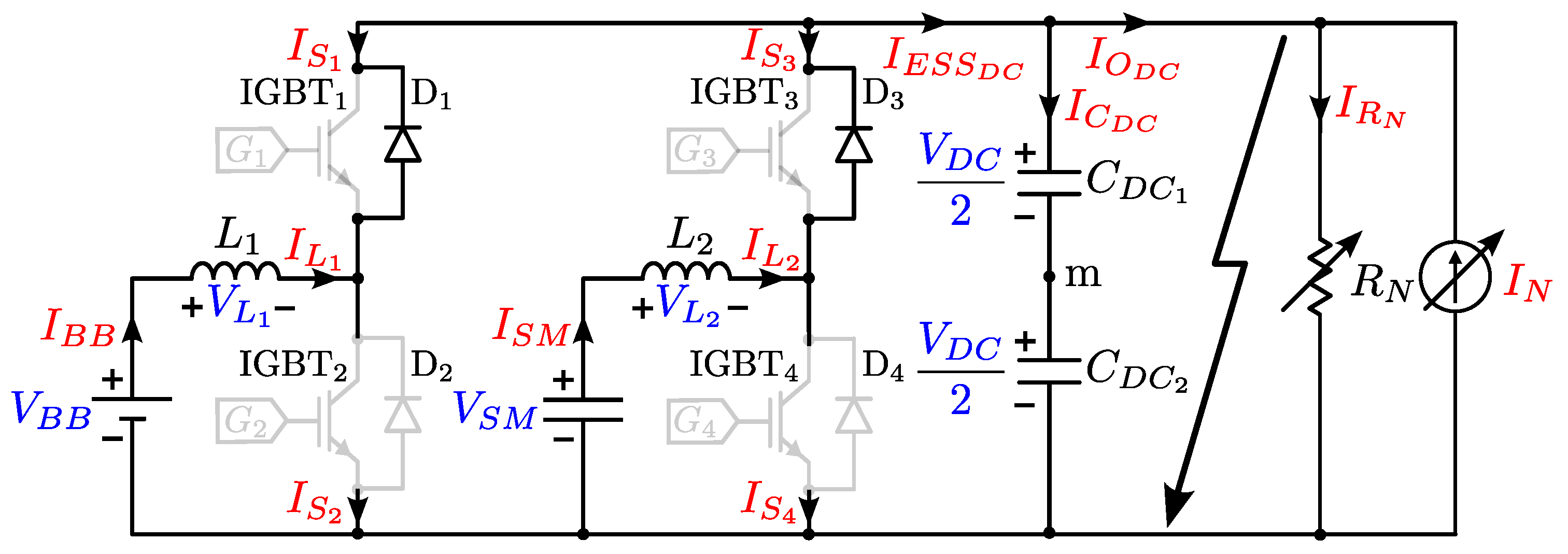
The simplest PEC topology for interfacing two energy storage devices that build up the HESS to a DC microgrid is the direct connection of two parallel bidirectional boost converters to the DC bus [7,11,12,13,14,15,16,17,18]. This scheme is depicted in Figure 1. This is a cost-effective and reliable solution for low to medium power range applications if galvanic isolation is not required, as the number of elements and devices is relatively low. The case under study considers the simple parallel connection of two distinct energy storage devices. One port consists of a lithium-ion Battery Bank (BB), which will provide a high energy density with slow dynamic response. The other port interfaces to a SM intended to support a high power density and faster dynamic response [5,11,12,13,14,15,16,17,19,20,21,22,23]. Therefore, provided that the control strategy is managed correctly, the resulting HESS has a better overall performance as compared to any of the individual systems. This ultimately provides a sustained, high-power, high-dynamic performance of the resulting storage system, also extending the BB lifetime [11,13,21,24].
In addition to the lack of galvanic isolation, a major disadvantage of this system is its sensitivity to short-circuit faults at the DC bus. If a short-circuit occurs, the current drawn from both the BB and the SM will increase without control, as the anti-parallel diodes of the upper switches in the legs of the boost converters would allow large short-circuit currents as depicted in Figure 2. This will cause damage to the inductors, the storage devices (BB and SM), and the switches themselves [3,4].
This work describes a new design approach for the power topology and control method which limits operation during DC side short-circuit faults. Even though the number of switching devices in the system is increased in order to build the power topology, the proposed control during the healthy condition achieves an operation without an increase in the losses compared to the two parallel bidirectional boost converters. In addition, the proposed control during the fault condition provides a protection to the converter and the EESs and afford a fast system recovery procedure so as to charge the DC bus once the fault has been cleared.
This paper is organized as follows: Section 2 proposes the buck-boost bidirectional circuit-based topology as a DC short-circuit fault-tolerant topology compared to the simplest boost-based solution shown in Figure 1. The control scheme for the aforementioned boost-based topology is analyzed, in order to establish a starting point in the discussion for the fault-tolerant control adaptation. Then, the control scheme adaptation for the parallel connection buck-boost topologies under consideration is proposed, both in healthy and fault conditions, respectively. After that, Section 3 shows the validation of the proposed system through simulations and experimental results to demonstrate the performance of the proposed solution. In this section, a comparison is also included between the original boost converters and the buck-boost solution. Finally, Section 4 summarizes the work done and discusses future developments.
2. Fault-Tolerant Topologies
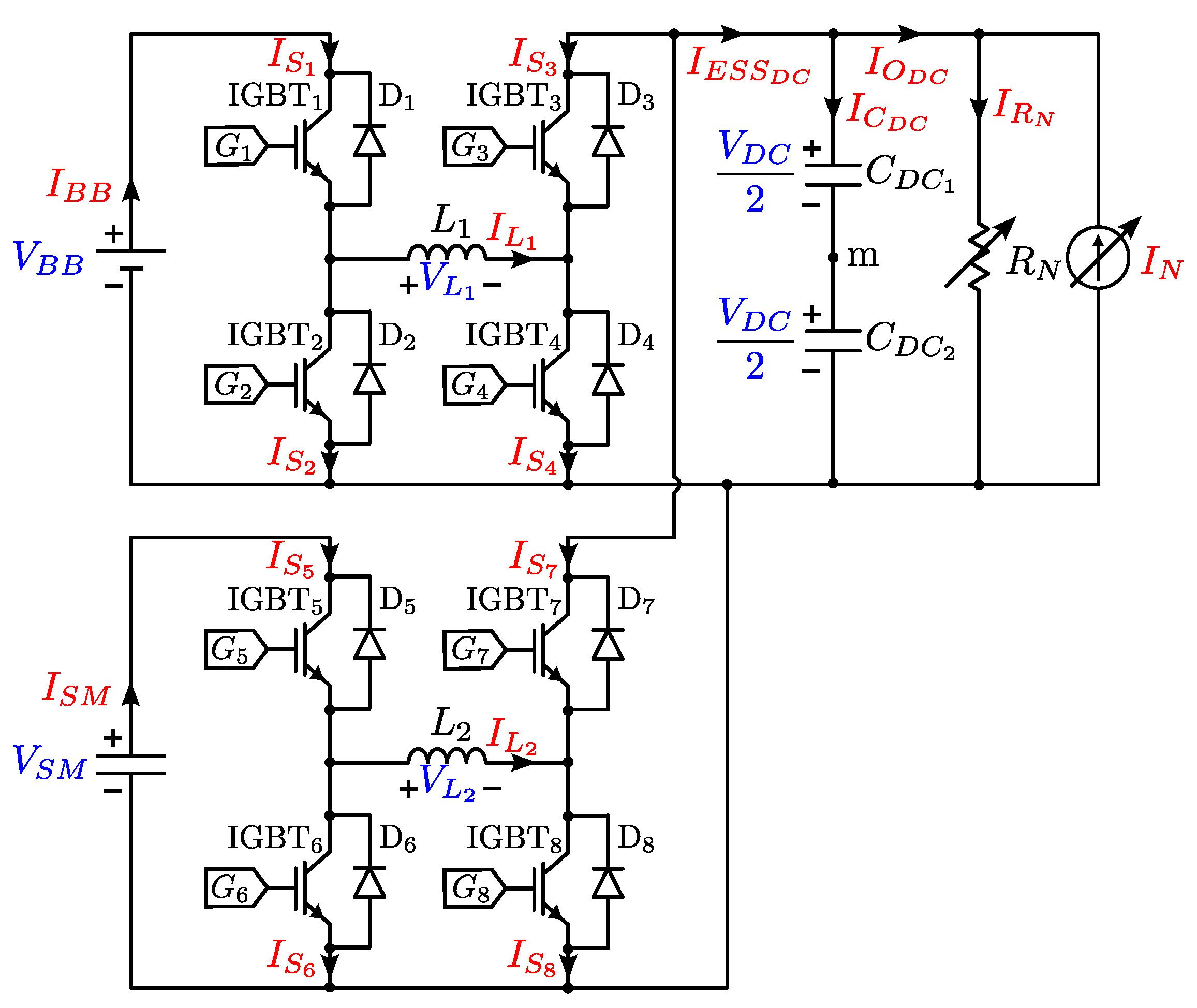
The solution to the DC bus fault behavior of the boost-based topology is the connection of a device able to interrupt, or at least limit, the fault currents flowing through the storage units. One option is to connect switches in series with the storage units and the inductors of the converters (see Figure 3). These switches can be opened during fault conditions to prevent the BB and SM short-circuit currents. In addition, to allow a discharge path for any current flowing through the inductors once the series switches are open, additional free-wheeling switches for each leg are required. Otherwise, a voltage spike will occur, causing arcing or even destruction of the switches. This yields to a final configuration of two parallel bidirectional buck-boost converters [25,26], as shown in Figure 4. This topology has not been analyzed for this particular challenge, i.e., fault tolerance in HESS.
Buck-boost converters can operate either as step-up or step-down voltage interface. In the system under consideration, configured as in Figure 4, the BB voltage () and the SM voltage () ratings are less than the DC bus voltage () and therefore the buck-boost converters will always operate as step-up converter. The main feature discussed in this work is the operation under fault condition of the HESS based on the buck-boost solution. Provided that a suitable control strategy is implemented, the proposed solution enables for a swift system reset once the fault is cleared. A proposal for such a fault ride-through feature will also be demonstrated in the following sections.
It can be seen that the inclusion of the short-circuit fault-tolerant features in the converter adds four more switches compared to the original topology (Figure 1), therefore resulting in higher cost and size than in the initial case. However, as it will be demonstrated in the following sections, by using a proper control, even though the number of switches has increased, the losses of the two topologies can be made very similar.
2.1. Analysis of the Boost Topology Based Control
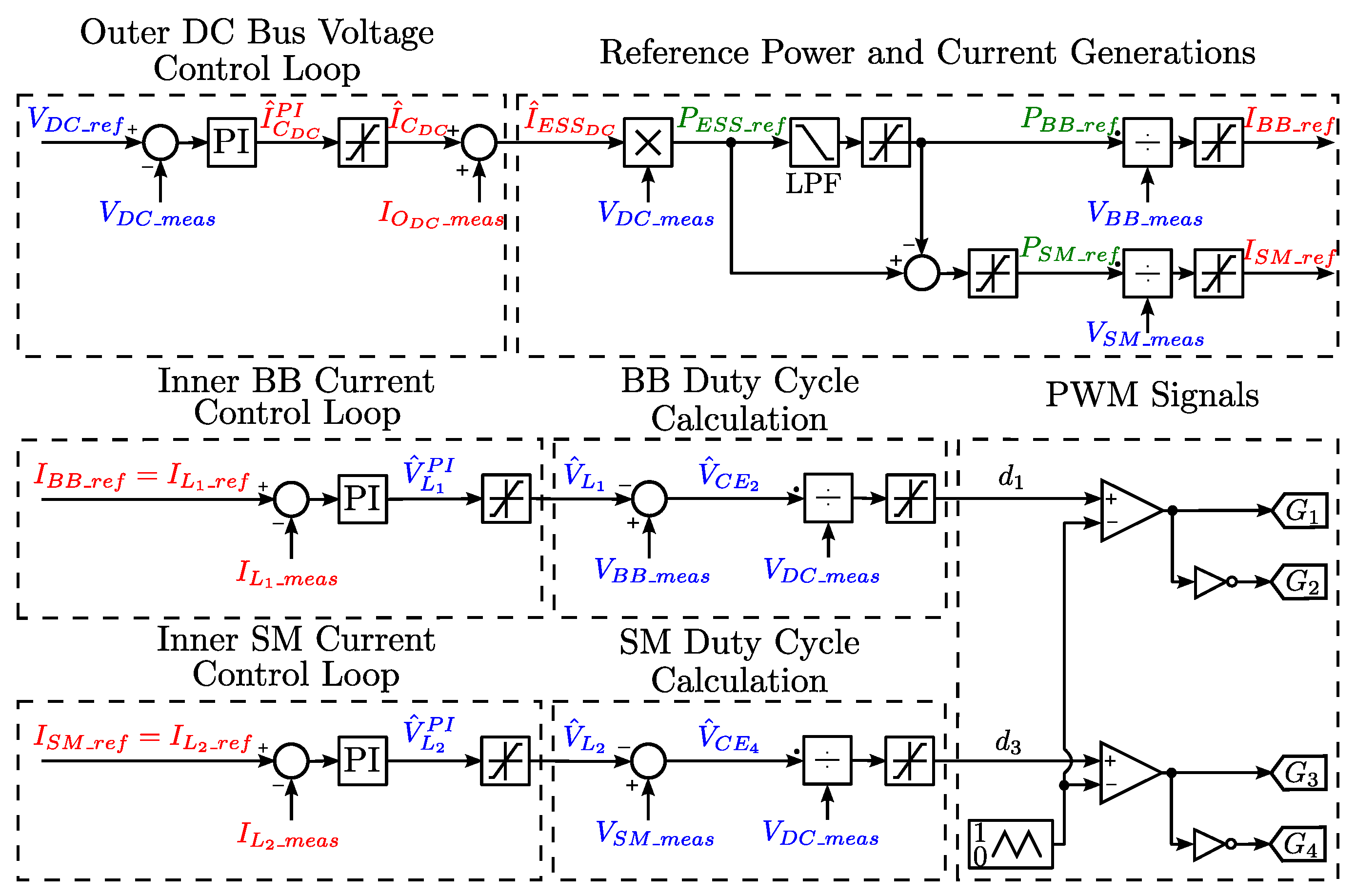
The case under consideration is a microgrid suitable to operate in islanding mode, with a HESS connected to the DC bus at the PCC, as depicted in Figure 4. In these conditions, a cascaded loop approach is used for the control of the power flows in the system. Both the BB and the SM converters are indeed controlled. The main goal of the control of the BB converter is to maintain the DC bus voltage constant, while the aim of the control of the SM converter is to provide or absorb transient power during load variations. The control strategy is implemented through three control loops: one outer voltage control loop that controls the DC bus voltage, plus two inner current loops in order to control the current flowing through the BB and SM inductors [12,13,16,22,27,28], as shown in Figure 5.
The outer voltage control loop is a Proportional-Integral (PI) controller to maintain the measured DC bus voltage () equal to the reference value (). Then, ESS power reference () is calculated from the control action of the voltage control loop () and the feed-forward term () to improve the recovery of the DC bus due to load variations. The limits of the control action are obtained as follows [29]:
where:
- and are the minimum and maximum current limits of the DC bus current in Amps,
- and are the minimum and maximum currents of the BB in Amps,
- and are the minimum and maximum currents of the SM in Amps,
- and are the minimum and maximum currents delivered by the rest of the microgrid in Amps,
- is the reference DC bus voltage in Volts,
- and are the minimum and maximum load powers in Watts.
The minimum BB and SM currents are the maximum BB and SM charging currents; however, the maximum BB and SM currents are the maximum BB and SM discharging currents. Then, the SM reference power () is calculated as the difference between the references for the ESS and BB power values ( and , respectively). A limiter is used to ensure that SM power limits are not exceeded. The BB power reference () is calculated by using a Low Pass Filter (LPF) to ensure that the SM is providing or absorbing the peak transient power during load variations [28]. Also another limiter is used here, to ensure that the SM provides (or absorbs) the excess power that BB cannot provide (or absorb) during steady state. The power references are calculated according to the following equations [28,30]:
where:
- , and are the reference powers of the ESS, BB and SM, respectively, in Watts,
- is the current in the DC bus (control action of the voltage controller) in Amps,
- is the measured output current of the two converters in Amps,
- is the measured DC bus voltage in Volts,
- is the time constant of the LPF in Secs,
- s is the Laplace complex variable .
The current references of the BB and SM are obtained by dividing their power references by the corresponding voltage. The bandwidth of the controller for the current in (inductor in SM converter) () is faster than the bandwidth of the controller for inductor (BB converter). This control scheme considers the inductors’ voltages, and in Figure 1 to be the control actions at the output of the current regulators. The limits for the inductor voltages can then be calculated as [29]:
where:
- , , and are the minimum and maximum inductor voltages for the BB and SM boost converters, respectively, in Volts,
- and are the measured storage device voltages in Volts.
Therefore an adaptation between these control actions and the applied duty cycles in both converters, and , is implemented in the control (Duty Cycle Calculation blocks in Figure 5).
where:
- and are the duty ratios of the BB and SM converters, respectively,
- and are the inductor voltages (control action of the current controller) for the BB and SM boost converters, respectively, in Volts.
2.2. Fault-Tolerant Converter Control Strategy for Normal Operation
Some modifications in the previous control are required in order to calculate the duty cycle from the output of the regulator for the buck-boost-based solution (Duty Cycles Calculation block), as shown in Figure 6. With this direct approach, the diagonal switches (S2 and S3) and (S6 and S7) will commutate with the values of the duty cycles for the BB and SM converters respectively, while the other diagonal switches (S1 and S4) and (S5 and S8) will switch in a complementary scheme.
The expressions to calculate the limits for the inductor voltages in this case are as follows:
The same procedure is implemented to calculate the duty ratio for both the BB and SM converters:
As discussed, all the switches are commutating at High Frequency (HF). This approach, though, will increase the switching losses and therefore the total efficiency of the system will drop. In order to maintain the efficiency, the proposed modifications in the control strategy makes use of two independent modes of operation for each converter during the healthy condition (Normal operation). These modes are Buck mode and Boost mode. This scheme aims to decrease the number of commutating switches in each converter, in order to consequently decrease the switching losses [31,32,33].
A triangular Pulse-Width Modulation (PWM) technique is implemented to obtain the switching patterns of the switches at the converter. However, in order to achieve a swift transition between the two switching modes, this modulation will be based on two different triangle carrier signals: one carrier for the Boost mode (using peak values of the triangular modulating waveform from 0.0 to 0.5), and another carrier for the Buck mode (using values from 0.5 to 1.0).
This structure implies no overlapping of the HF switching intervals, which yields two different switching patterns for the switches. For example (as shown in Figure 7), if the desired duty cycle is between 0.0 and 0.5, the bidirectional buck-boost converter operates in Boost mode, and therefore switches S2 and S6 are turned off, while switches S1 and S5 remain turned on continuously. The switches S3 and S7 switch with the value of the duty cycle and the switches S4 and S8 are their complement. For the Buck mode, when the duty cycle is between 0.5 and 1.0, switches S3 and S7 are turned on and switches S4 and S8 remain off continuously. S1 and S5 switch with value of the duty cycle and S2 and S6 are their complement. Figure 8 depicts the implementation of this dual carrier control for the two parallel bidirectional buck-boost converters. The limits of the inductor voltage are the same as in the case of the boost converter (6)–(9).
2.3. Fault-Tolerant Converter Control Strategy under DC-Link Fault Operation
The most critical short-circuit fault types in DC microgrids are either short-circuit between positive and negative bus bars, or a short-circuit between any bus bar and ground [34]. In the first approach of the proposed control scheme, once a DC bus short-circuit fault is detected (for instance by detecting a DC bus voltage below a threshold level), all the switches of the storage converters will be turned off. Therefore the storage devices are instantly disconnected from the DC bus while allowing a discharge path for the inductors at the converters through the anti-parallel diodes of the switches. After the inductances are discharged, no more energy is interchanged between the HESS and the DC bus. However, this control scheme does not have ride-through capability, and therefore even if the fault is removed, the system by itself has no ability of returning to the initial operation mode, unless the control is reset manually and the DC bus is charged externally. After the DC bus is back at rated values, the control scheme works again, and the HESS will remain to support the microgrid normal operation. This scheme is shown in Figure 9.
However, by making a relatively simple modification to the control scheme, the converter can still operate in a controlled manner under fault conditions and can resume normal healthy operation once the fault is over. This modification is introduced in Figure 10.
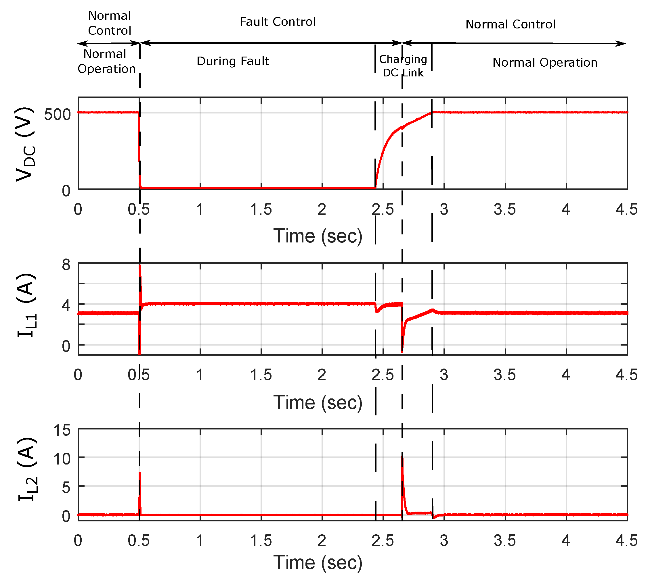
The fault sequence operation of this control scheme is outlined in Figure 11. The DC bus fault occurs at . Then, the fault ride-through capability of the proposed strategy is achieved by providing a small safe current reference () value for the BB converter only under DC bus short-circuit. While the DC bus fault is still present, the DC bus voltage remains nearly zero. However, this small current enables the DC bus capacitance to charge linearly once the fault is cleared at . Once a threshold value is reached at , the system gets back to the normal operation scheme, and the standard control takes the system back to the steady state at . This current reference value must be low enough as not to discharge the BB in a reasonable time frame. On the other side, this value must be large enough as to allow a fast detection of the fault clearance condition. Ultimately, this reference value is a function of the DC bus voltage rating and the DC bus capacitance.
The current reference is automatically implemented considering that the voltage across the inductor is limited, and therefore the duty cycle for BB is given by (19) to (21). It also must be noticed that if the fault is permanent, the control is designed to operate for a specific time and then the switches of the BB converters will be turned off in order to decrease the power dissipated from the BB. Another advantage is that this control can be used to charge the DC bus at system start-up. During fault and fault ride-through intervals, the switches of the SM converter are turned off, and SM current is null.
3. System Parameters and Validation through Simulation and Experimental Results
This section covers the main specifications of the system parameters, the design of the control parameters as well as the validation achieved through simulations of the system performance and a related experimental setup. Simulations of the full system operation have been carried out with MATLAB/SIMULINK/PLECS.
3.1. Main Operating Parameters
Although the conclusions from the prior discussion are valid in general, the validation of such conclusions is demonstrated in a specific laboratory setup that is described in Table 1. The specific control algorithms have been designed and tuned for this particular setup. Once the setup and the control algorithms are defined, then the system performance can be validated through the analysis of both simulations and experimental results.
3.2. Design of the Regulators in the Control Loops
The control scheme has three PI controllers in the outer DC bus voltage control loop and the two inner current control loops for BB and SM. Considering the ideal form of PI controller which is tuned by zero-pole cancellation, the transfer function is given by:
where:
- is the transfer function of the PI controller,
- is the proportional gain,
- is the integral time constant.
Current controllers have been tuned by zero-pole cancellation, whereas voltage controller is tuned by loop-shaping techniques.
The control parameters of the converters are listed in Table 2. Taking into account that the bandwidth of the SM current PI controller () is faster that the bandwidth of the BB current PI controller (). Both bandwidths are faster than the bandwidth of voltage PI controller ().
3.3. Comparison in Terms of Losses
Special attention has been put on the calculation of the losses in the switches (both conduction and switching losses) during the normal operation of the converters. The conduction and the switching losses of the switches are calculated according to [29]:
where:
- , and are the average conduction losses of the switch, IGBT and the anti-parallel diode, respectively, in Watts,
- is the switching time in Secs,
- is the on-state collector emitter voltage of the IGBT in Volts,
- is the on-state collector current of the IGBT in Amps,
- is on-state forward voltage of the anti-parallel diode in Volts.
- , and are the switching losses of the switch, the IGBT and the anti-parallel diode, respectively, in Watts,
- and are the energy loss at IGBT turn on and turn off, respectively, in Joules,
- is the switching frequency in Hz,
- is the energy loss of the reverse recovery of the anti-parallel diode in Joules.
Once these calculations are considered, a comparison between the original boost topology and the new buck-boost topology with both switching schemes (single and dual carrier) has been carried out in PLECS by using the datasheet of the IGBTs (2MBI200HH-120-50 from Fuji Electric) based on the equations explained before. As can be seen from Table 3, the overall losses (both switching and conduction losses) using the fault-tolerant topology with the standard switching pattern are higher than in the original boost-based solution. Still looking at Table 3, it can be noticed how the switching losses at the fault-tolerant topology using the proposed dual carrier control scheme are almost equal to the ones at the original boost-based topology converter. It can also be seen how the conduction losses are higher in the former case, given that S1 and S5 are continuously turned on. Therefore, it can be concluded that the total losses at the fault-tolerant solution with the dual carrier scheme are quite similar to the original boost converter case.
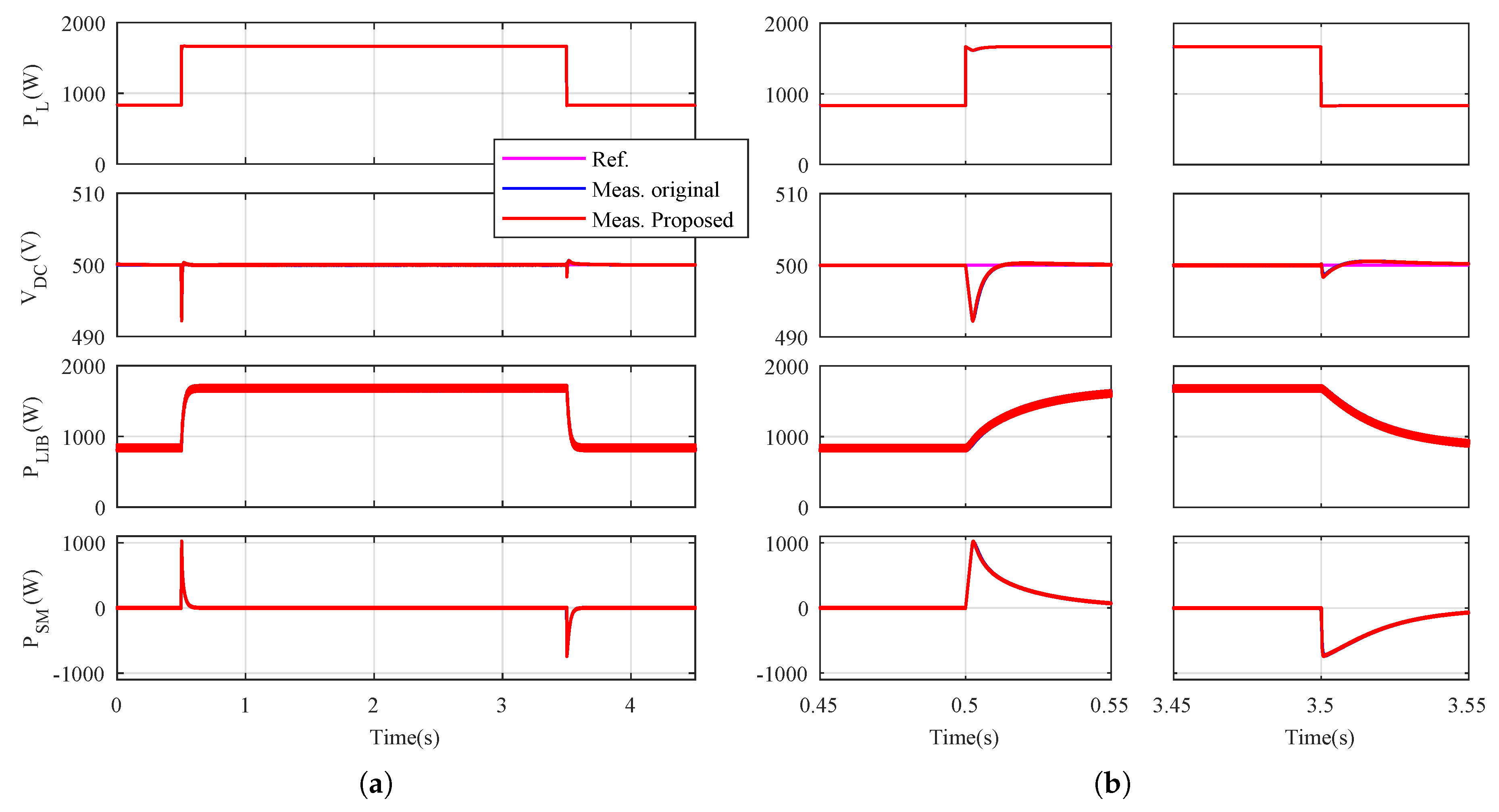
Figure 12 shows the operation of both the boost topology and the buck-boost solution with the dual carrier scheme, under healthy conditions. The figure shows that these two solutions give the same performance during transient load steps. The BB controls the DC bus around 500 V, while the SM delivers and absorbs the transient power required during the load steps (from 833.3 W to 1666.7 W and again to 833.3 W) to avoid DC bus voltage variation during the transients. This yields to a fast recovery of the DC bus voltage as well as to a decrease in the power ratings and the stresses (including current ripple) in the battery.
The fault ride-through capability of the buck-boost converter with the proposed dual carrier control is shown in Figure 13. The converters are initially operating under normal control; however, when a DC bus fault is detected at 0.5 s (the DC bus voltage below 15 V threshold), the converters operate under fault control. In fault control mode, a 4 A reference current (value chosen for demonstration purposes) is applied to the BB, while the SM leg is disconnected. When the fault is removed at 2.5 s, this reference will charge the DC bus to a specific value (500 V threshold in this case). Then, the system is automatically reset to the normal control. The DC bus will continue charging linearly until the DC bus reference voltage value and the converter operate in normal mode. The higher current reference, the faster the DC bus charging after fault is removed. This means more unuseful power burned during the fault. At the end, it is a tradeoff depending on the DC bus voltage value, the capacitance value and how fast to charge the DC bus after fault is cleared.
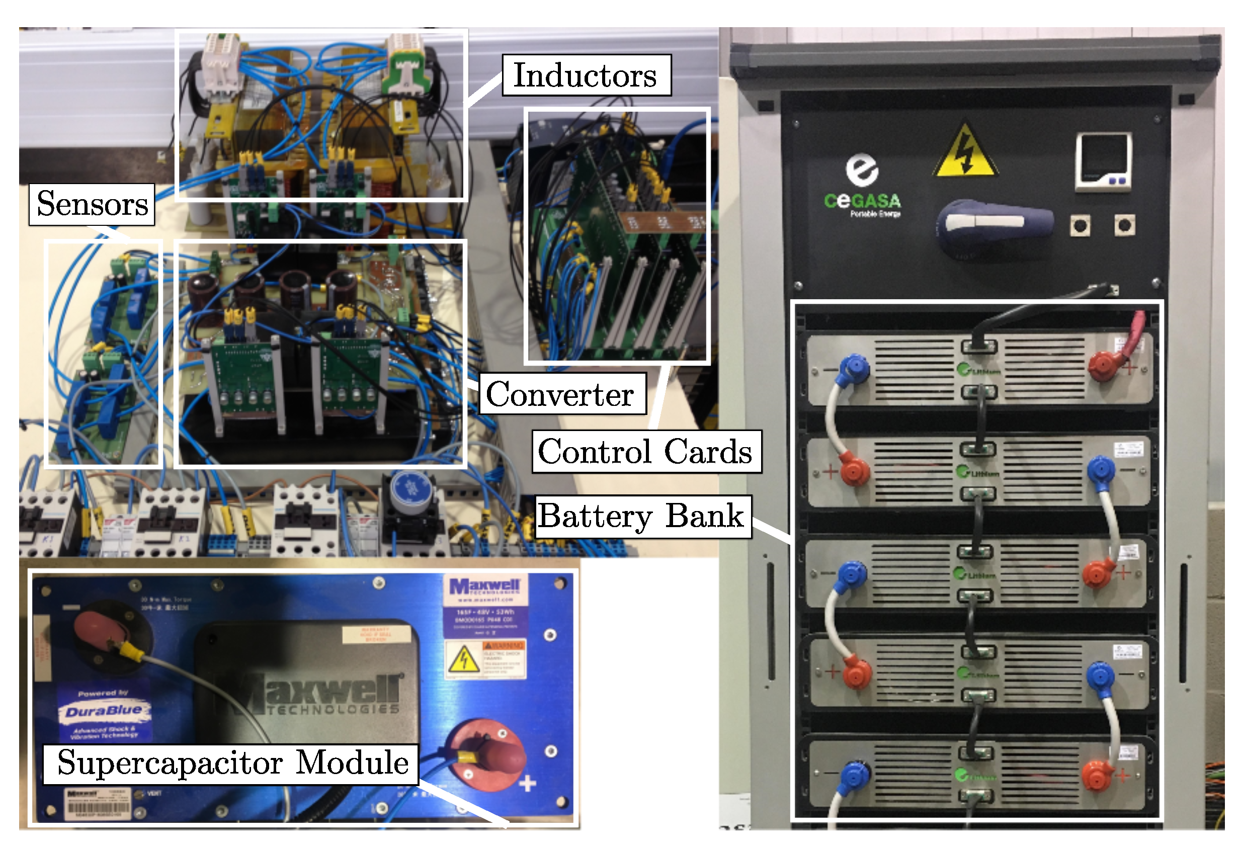
3.4. Experimental Validation of the System Performance
The proposed control scheme in the fault-tolerant topology has been validated using the experimental setup as shown in Figure 14. Figure 15 shows the normal operation of the two parallel bidirectional boost converters and the two parallel bidirectional buck-boost converters. The load is changed at 0.5 s from 833.3 W to 1666.7 W and at 3.6 s is changed again to 833.3W. Figure 15 fully matches with the simulation results in Figure 12. Figure 16 show the operation of the buck-boost converter with the proposed control during the normal operation and fault operation and again fully matches with Figure 13 from simulations. The fault is occurred at 0.5 s and is cleared at 2.4 s.
4. Conclusions and Future Developments
In this paper, a DC bus short-circuit fault-tolerant control scheme for a non-isolated topology for HESSs has been presented, analyzed, verified through simulations and experimentally demonstrated. The proposed control prevents the ESSs and the converter from the damage of the short-circuit current. The proposed strategy includes automatic fault ride-through once the DC bus short-circuit is cleared which helps the converter to operate smoothly in the healthy condition. This configuration has a higher component count than the bidirectional boost version, which is the simplest topology able to achieve the required dynamic performance. However, provided that the proposed dual carrier control scheme during the healthy condition is used, it has been demonstrated that the inclusion of the fault-tolerant, fault ride-through feature does not significantly increase the overall power losses. The proposed configuration, based on the two carrier signals can operate in buck or boost mode, making this scheme also useful for different applications in which the voltage of the ESSs is higher or lower than that of the DC bus.
Future developments include the extension of the study to other fault types, for instance at the storage units; optimization of the control parameters to minimize the energy lost during fault mode; or the extension of this scheme to other kind of applications apart from HESS.
Author Contributions
R.G., J.G. and M.S. conceived the research, designed and performed the experiments; All the authors analyzed the data, and contributed in the discussion and conclusions. All authors have read and agreed to the published version of the manuscript.
Funding
This work has been partially supported by the Spanish Government, Innovation Development and Research Office (MEC), under research grant ENE2016-77919, Project “Conciliator”, and by the European Union through ERFD Structural Funds (FEDER). This work has been partially supported by the government of Principality of Asturias, Foundation for the Promotion in Asturias of Applied Scientific Research and Technology (FICYT), under Grant FC-GRUPIN-IDI/2018/000241 and under Severo Ochoa research grants, PA-13-PF-BP13-138 and PF-BP16-133.
Conflicts of Interest
The authors declare no conflict of interest. The founding sponsors had no role in the design of the study; in the collection, analyses, or interpretation of data; in the writing of the manuscript, and in the decision to publish the results.
Abbreviations
The following abbreviations are used in this manuscript:
| HESS | Hybrid Energy Storage System |
| PCC | Point of Common Coupling |
| PEC | Power Electronic Converter |
| ESSs | Energy Storage Systems |
| SM | Supercapacitor Module |
| BB | Battery Bank |
| PI | Proportional-Integral |
| LPF | Low Pass Filter |
| HF | High Frequency |
| PWM | Pulse-Width Modulation |
The following symbols are used in this manuscript:
| BB voltage | V | |
| SM voltage | V | |
| DC bus voltage | V | |
| Inductor voltages for the BB | V | |
| Inductor voltages for the SM | V | |
| On-state collector emitter voltage of the IGBT | V | |
| On-state forward voltage of the anti-parallel diode | V | |
| DC bus current | A | |
| Output current of the two converters | A | |
| BB current | A | |
| SM current | A | |
| Current delivered by the rest of the microgrid | A | |
| On-state collector current of the IGBT | A | |
| ESS power | kW | |
| BB power | kW | |
| SM power | kW | |
| Load power | kW | |
| Average conduction losses of the switch | kW | |
| Switching losses of the switch | kW | |
| Duty ratio of the BB converter | ||
| Duty ratio of the SM converter | ||
| Capacitance of the SM | F | |
| Capacitance of the DC bus | F | |
| Inductance of the inductor connected to the BB | mH | |
| Inductance of the inductor connected to the SM | mH | |
| Resistance of the inductor connected to the BB | ||
| Resistance of the inductor connected to the SM | ||
| Transfer function of the PI controller | ||
| s | Laplace complex variable | |
| Proportional gain | ||
| Integral time constant | s | |
| Time constant of the LPF | s | |
| Switching time | s | |
| Switching frequency | Hz | |
| Bandwidth of the PI controller | Hz | |
| Energy loss at IGBT turn on | J | |
| Energy loss at IGBT turn off | J | |
| Energy loss of the reverse recovery of the anti-parallel diode | J |
References
- Lasseter, R.H. Smart Distribution: Coupled Microgrids. Proc. IEEE 2011, 99, 1074–1082. [Google Scholar] [CrossRef]
- Dugan, R.; McGranaghan, M.; Santoso, S.; Beaty, H. Electrical Power Systems Quality; McGraw-Hill Education: New York, NY, USA, 2012. [Google Scholar]
- Bui, D.M.; Chen, S.L.; Wu, C.H.; Lien, K.Y.; Huang, C.H.; Jen, K.K. Review on protection coordination strategies and development of an effective protection coordination system for DC microgrid. In Proceedings of the 2014 IEEE PES Asia-Pacific Power and Energy Engineering Conference (APPEEC), Hong Kong, China, 7–10 December 2014; pp. 1–10. [Google Scholar] [CrossRef]
- Dragičević, T.; Lu, X.; Vasquez, J.C.; Guerrero, J.M. DC Microgrids—Part II: A Review of Power Architectures, Applications, and Standardization Issues. IEEE Trans. Power Electron. 2016, 31, 3528–3549. [Google Scholar] [CrossRef] [Green Version]
- Tan, X.; Li, Q.; Wang, H. Advances and Trends of Energy Storage Technology in Microgrid. Int. J. Electr. Power Energy Syst. 2013, 44, 179–191. [Google Scholar] [CrossRef]
- Jing, W.; Lai, C.H.; Wong, S.H.W.; Wong, M.L.D. Battery-supercapacitor hybrid energy storage system in standalone DC microgrids: A review. IET Renew. Power Gener. 2017, 11, 461–469. [Google Scholar] [CrossRef]
- Cao, J.; Emadi, A. A New Battery/UltraCapacitor Hybrid Energy Storage System for Electric, Hybrid, and Plug-In Hybrid Electric Vehicles. IEEE Trans. Power Electron. 2012, 27, 122–132. [Google Scholar] [CrossRef]
- Ortuzar, M.; Moreno, J.; Dixon, J. Ultracapacitor-Based Auxiliary Energy System for an Electric Vehicle: Implementation and Evaluation. IEEE Trans. Ind. Electron. 2007, 54, 2147–2156. [Google Scholar] [CrossRef]
- Xiao, J.; Wang, P.; Setyawan, L. Multilevel Energy Management System for Hybridization of Energy Storages in DC Microgrids. IEEE Trans. Smart Grid 2016, 7, 847–856. [Google Scholar] [CrossRef]
- Maharjan, L.; Yamagishi, T.; Akagi, H.; Asakura, J. Fault-Tolerant Operation of a Battery-Energy-Storage System Based on a Multilevel Cascade PWM Converter With Star Configuration. IEEE Trans. Power Electron. 2010, 25, 2386–2396. [Google Scholar] [CrossRef]
- Tummuru, N.R.; Mishra, M.K.; Srinivas, S. Dynamic Energy Management of Hybrid Energy Storage System With High-Gain PV Converter. IEEE Trans. Energy Convers. 2015, 30, 150–160. [Google Scholar] [CrossRef]
- Kollimalla, S.K.; Mishra, M.K.; Narasamma, N.L. Design and Analysis of Novel Control Strategy for Battery and Supercapacitor Storage System. IEEE Trans. Sustain. Energy 2014, 5, 1137–1144. [Google Scholar] [CrossRef]
- Kollimalla, S.K.; Mishra, M.K.; N, L.N. Coordinated Control and Energy Management of Hybrid Energy Storage System in PV System. In Proceedings of the 2014 International Conference on Computation of Power, Energy, Information and Communication (ICCPEIC), Chennai, India, 16–17 April 2014; pp. 363–368. [Google Scholar] [CrossRef]
- Sathishkumar, R.; Kollimalla, S.K.; Mishra, M.K. Dynamic Energy Management of Micro Grids Using Battery Super Capacitor Combined Storage. In Proceedings of the 2012 Annual IEEE India Conference (INDICON), Kochi, India, 7–9 December 2012; pp. 1078–1083. [Google Scholar] [CrossRef]
- Jayasinghe, S.D.G.; Vilathgamuwa, D.M.; Madawala, U.K. A Direct Integration Scheme for Battery-Supercapacitor Hybrid Energy Storage Systems with the Use of Grid Side Inverter. In Proceedings of the 2011 Twenty-Sixth Annual IEEE Applied Power Electronics Conference and Exposition (APEC), Fort Worth, TX, USA, 6–11 March 2011; pp. 1388–1393. [Google Scholar] [CrossRef]
- Li, W.; Joos, G.; Belanger, J. Real-Time Simulation of a Wind Turbine Generator Coupled with a Battery Supercapacitor Energy Storage System. IEEE Trans. Ind. Electron. 2010, 57, 1137–1145. [Google Scholar] [CrossRef]
- Yoo, H.; Sul, S.K.; Park, Y.; Jeong, J. System Integration and Power-Flow Management for a Series Hybrid Electric Vehicle Using Supercapacitors and Batteries. IEEE Trans. Ind. Appl. 2008, 44, 108–114. [Google Scholar] [CrossRef]
- Vazquez, S.; Lukic, S.M.; Galvan, E.; Franquelo, L.G.; Carrasco, J.M. Energy Storage Systems for Transport and Grid Applications. IEEE Trans. Ind. Electron. 2010, 57, 3881–3895. [Google Scholar] [CrossRef] [Green Version]
- Li, W.; Joos, G. A Power Electronic Interface for a Battery Supercapacitor Hybrid Energy Storage System for Wind Applications. In Proceedings of the 2008 IEEE Power Electronics Specialists Conference (PESC), Rhodes, Greece, 15–19 June 2008; pp. 1762–1768. [Google Scholar] [CrossRef]
- Khaligh, A.; Li, Z. Battery, Ultracapacitor, Fuel Cell, and Hybrid Energy Storage Systems for Electric, Hybrid Electric, Fuel Cell, and Plug-In Hybrid Electric Vehicles: State of the Art. IEEE Trans. Veh. Technol. 2010, 59, 2806–2814. [Google Scholar] [CrossRef]
- Solero, L.; Lidozzi, A.; Pomilio, J.A. Design of Multiple-Input Power Converter for Hybrid Vehicles. IEEE Trans. Power Electron. 2005, 20, 1007–1016. [Google Scholar] [CrossRef]
- Mendis, N.; Muttaqi, K.M.; Perera, S. Active Power Management of a Super Capacitor-Battery Hybrid Energy Storage System for Standalone Operation of DFIG based Wind Turbines. In Proceedings of the 2012 IEEE Industry Applications Society Annual Meeting (IAS), Las Vegas, NV, USA, 7–11 October 2012; pp. 1–8. [Google Scholar] [CrossRef]
- Gee, A.M.; Robinson, F.V.P.; Dunn, R.W. Analysis of Battery Lifetime Extension in a Small-Scale Wind-Energy System Using Supercapacitors. IEEE Trans. Energy Convers. 2013, 28, 24–33. [Google Scholar] [CrossRef]
- van Voorden, A.M.; Elizondo, L.M.R.; Paap, G.C.; Verboomen, J.; van der Sluis, L. The Application of Super Capacitors to relieve Battery-storage systems in Autonomous Renewable Energy Systems. In Proceedings of the 2007 IEEE Lausanne Power Tech, Lausanne, Switzerland, 1–5 July 2007; pp. 479–484. [Google Scholar] [CrossRef] [Green Version]
- Tytelmaier, K.; Husev, O.; Veligorskyi, O.; Yershov, R. A Review of Non-Isolated Bidirectional DC-DC Converters for Energy Storage Systems. In Proceedings of the 2016 II International Young Scientists Forum on Applied Physics and Engineering (YSF), Kharkiv, Ukraine, 10–14 October 2016; pp. 22–28. [Google Scholar] [CrossRef]
- Du, Y.; Zhou, X.; Bai, S.; Lukic, S.; Huang, A. Review of Non-isolated Bi-directional DC-DC Converters for Plug-in Hybrid Electric Vehicle Charge Station Application at Municipal Parking Decks. In Proceedings of the 2010 Twenty-Fifth Annual IEEE Applied Power Electronics Conference and Exposition (APEC), Palm Springs, CA, USA, 21–25 February 2010; pp. 1145–1151. [Google Scholar] [CrossRef]
- Silva, M.A.; de Melo, H.N.; Trovao, J.P.; Pereirinha, P.G.; Jorge, H.M. Hybrid Topologies Comparison for Electric Vehicles with Multiple Energy Storage Systems. In Proceedings of the 2013 World Electric Vehicle Symposium and Exhibition (EVS27), Barcelona, Spain, 17–20 November 2013; pp. 1–8. [Google Scholar] [CrossRef]
- Georgious, R.; García, J.; García, P.; Sumner, M. Analysis of hybrid energy storage systems with DC link fault ride-through capability. In Proceedings of the 2016 IEEE Energy Conversion Congress and Exposition (ECCE), Milwaukee, WI, USA, 18–22 September 2016; pp. 1–8. [Google Scholar] [CrossRef] [Green Version]
- Georgious, R. A Hybrid Solution for Distributed Energy Storage for Microgeneration in Microgrids: Design of the Electronic Power and Control System. Ph.D. Thesis, University of Oviedo, Oviedo, Spain, 2018. [Google Scholar]
- Wang, C.S.; Li, W.; Wang, Y.F.; Han, F.Q.; Meng, Z.; Li, G.D. An Isolated Three-Port Bidirectional DC-DC Converter with Enlarged ZVS Region for HESS Applications in DC Microgrids. Energies 2017, 10, 446. [Google Scholar] [CrossRef] [Green Version]
- Lee, Y.J.; Khaligh, A.; Emadi, A. A Compensation Technique for Smooth Transitions in a Noninverting Buck–Boost Converter. IEEE Trans. Power Electron. 2009, 24, 1002–1015. [Google Scholar] [CrossRef]
- Aharon, I.; Kuperman, A.; Shmilovitz, D. Analysis of Dual-Carrier Modulator for Bidirectional Noninverting Buck–Boost Converter. IEEE Trans. Power Electron. 2015, 30, 840–848. [Google Scholar] [CrossRef]
- Wei, C.L.; Chen, C.H.; Wu, K.C.; Ko, I.T. Design of an Average-Current-Mode Noninverting Buck–Boost DC–DC Converter With Reduced Switching and Conduction Losses. IEEE Trans. Power Electron. 2012, 27, 4934–4943. [Google Scholar] [CrossRef]
- Salomonsson, D.; Soder, L.; Sannino, A. Protection of Low-Voltage DC Microgrids. IEEE Trans. Power Deliv. 2009, 24, 1045–1053. [Google Scholar] [CrossRef]
Figure 1.
Two parallel bidirectional boost converters connected to BB and SM and sharing the DC bus.
Figure 1.
Two parallel bidirectional boost converters connected to BB and SM and sharing the DC bus.

Figure 2.
Short-circuit fault at the DC bus of the two bidirectional boost converters.

Figure 3.
Two parallel bidirectional boost converters with a switch in series between the storage devices and inductors.
Figure 3.
Two parallel bidirectional boost converters with a switch in series between the storage devices and inductors.

Figure 4.
Two parallel bidirectional buck-boost converters connected to BB and SM and sharing the DC bus.
Figure 4.
Two parallel bidirectional buck-boost converters connected to BB and SM and sharing the DC bus.

Figure 5.
Control of the two parallel bidirectional boost converters to maintain the DC bus voltage constant (BB converter) and provide or absorb transient power during load variations (SM converter).
Figure 5.
Control of the two parallel bidirectional boost converters to maintain the DC bus voltage constant (BB converter) and provide or absorb transient power during load variations (SM converter).

Figure 6.
Control of two parallel bidirectional buck-boost converters with the same carrier to maintain the DC bus voltage constant (BB converter) and provide or absorb transient power during load variations (SM converter).
Figure 6.
Control of two parallel bidirectional buck-boost converters with the same carrier to maintain the DC bus voltage constant (BB converter) and provide or absorb transient power during load variations (SM converter).

Figure 7.
PWM of the two parallel bidirectional buck-boost converters based on two different carriers.
Figure 7.
PWM of the two parallel bidirectional buck-boost converters based on two different carriers.

Figure 8.
Control of the two parallel bidirectional buck-boost converters with two different carriers to maintain the DC bus voltage constant (BB converter) and provide or absorb transient power during load variations (SM converter).
Figure 8.
Control of the two parallel bidirectional buck-boost converters with two different carriers to maintain the DC bus voltage constant (BB converter) and provide or absorb transient power during load variations (SM converter).

Figure 9.
Control scheme including the fault detection block and the pulse disabling.

Figure 10.
Proposed control of the two parallel bidirectional buck-boost converters during the DC bus fault.
Figure 10.
Proposed control of the two parallel bidirectional buck-boost converters during the DC bus fault.

Figure 11.
Performance of the fault ride-through control sequence.

Figure 12.
Simulation results during normal operation for the original topology (blue) and the proposed one (red) where: (a) the load power () is changed from 833.3 W to 1666.7 W and then to 833.3 W again. (b) zoom at these changes.
Figure 12.
Simulation results during normal operation for the original topology (blue) and the proposed one (red) where: (a) the load power () is changed from 833.3 W to 1666.7 W and then to 833.3 W again. (b) zoom at these changes.

Figure 13.
Simulation results during fault and healthy conditions with the proposed control, the fault occurred at 0.5 s and cleared at 2.5 s.
Figure 13.
Simulation results during fault and healthy conditions with the proposed control, the fault occurred at 0.5 s and cleared at 2.5 s.

Figure 14.
Experimental setup of four legs of IGBTs and can be connected to be boost converter or buck-boost converter.
Figure 14.
Experimental setup of four legs of IGBTs and can be connected to be boost converter or buck-boost converter.

Figure 15.
Experimental results during normal operation for the original topology (blue) and the proposed one (red) where: (a) the load power () is changed from 833.3 W to 1666.7 W and then to 833.3 W again. (b) zoom at these changes.
Figure 15.
Experimental results during normal operation for the original topology (blue) and the proposed one (red) where: (a) the load power () is changed from 833.3 W to 1666.7 W and then to 833.3 W again. (b) zoom at these changes.

Figure 16.
Experimental results during fault and normal operation with the proposed control, the fault occurred at 0.5 s and cleared at 2.4 s.
Figure 16.
Experimental results during fault and normal operation with the proposed control, the fault occurred at 0.5 s and cleared at 2.4 s.


Table 1.
Parameters of the converters.
| Parameter | Symbol | Value | Units |
|---|---|---|---|
| Nominal BB voltage | 300 | V | |
| Nominal SM voltage | 96 | V | |
| Capacitance of the SM | 165 | F | |
| DC bus voltage | 500 | V | |
| Capacitance of the DC bus | 470 | F | |
| Maximum load power | 2 | kW | |
| Inductance of the inductors | , | 21 | mH |
| Resistance of the inductors | , | 0.3 |
Table 2.
Parameters of the control of the converters.
| Parameter | Symbol | Value | Units |
|---|---|---|---|
| Outer DC Bus Voltage Control Loop | |||
| Bandwidth | 30 | Hz | |
| Proportional gain | 0.088548 | ||
| Integral time | 0.141 | s | |
| Inner BB Current Control Loop | |||
| Bandwidth | 300 | Hz | |
| Proportional gain | 39.564 | ||
| Integral time | 0.0438 | s | |
| Inner SM Current Control Loop | |||
| Bandwidth | 500 | Hz | |
| Proportional gain | 65.94 | ||
| Integral time | 0.0438 | s | |
| Cut off frequency of LPF | 8 | Hz | |
| Switching frequency | 20 | kHz | |
Table 3.
The losses in the topologies.
| Topology | Conduction Losses (W) | Switching Losses (W) | Total losses (W) |
|---|---|---|---|
| Boost | 10.67 | 49.93 | 60.61 |
| Buck-Boost (original switching mode) | 29.7 | 96 | 125.7 |
| Buck-Boost (proposed control mode) | 22.2 | 49.93 | 72.13 |
© 2020 by the authors. Licensee MDPI, Basel, Switzerland. This article is an open access article distributed under the terms and conditions of the Creative Commons Attribution (CC BY) license (http://creativecommons.org/licenses/by/4.0/).
Share and Cite
MDPI and ACS Style
Georgious, R.; Garcia, J.; Sumner, M.; Saeed, S.; Garcia, P. Fault Ride-Through Power Electronic Topologies for Hybrid Energy Storage Systems. Energies 2020, 13, 257. https://doi.org/10.3390/en13010257
AMA Style
Georgious R, Garcia J, Sumner M, Saeed S, Garcia P. Fault Ride-Through Power Electronic Topologies for Hybrid Energy Storage Systems. Energies. 2020; 13(1):257. https://doi.org/10.3390/en13010257
Chicago/Turabian StyleGeorgious, Ramy, Jorge Garcia, Mark Sumner, Sarah Saeed, and Pablo Garcia. 2020. "Fault Ride-Through Power Electronic Topologies for Hybrid Energy Storage Systems" Energies 13, no. 1: 257. https://doi.org/10.3390/en13010257
Note that from the first issue of 2016, this journal uses article numbers instead of page numbers. See further details here.