1. Introduction
Traditionally, in variable AC power system, load voltage and frequency regulation are accomplished with indirect AC-to-AC power converters as reported in [
1,
2,
3]. They are dual converters, having bulky DC linked capacitor to suppress the ripples in the output voltage of the first conversion stage. This arrangement generates harmonics in the input current, thus causing poor power quality. A filtering inductor filter is employed at the input side to mitigate the generated harmonics. Extra circuit elements (two inductors and capacitors) are employed in z-source arrangement [
4] to solve the short problem of the second conversion stage. Indirect AC power converters are complex and have high conversion losses, thus causing poor efficiency. Their reliability is also low, due to an intermediate DC link capacitor [
5].
In direct AC-to-AC power converters [
6,
7,
8], the variable output voltage and the frequency are obtained through a single stage power conversion. These can be implemented as AC voltage controllers and direct frequency changers (DFC). They offer many advantages, such as simple circuit implementation, easier control, small size, and low price. AC voltage controllers are used to control the dynamic voltage variation in AC power systems. Voltage sags and swells are major disturbances of the power system [
9], which degrade the system’s performance severely. The end users have to use power-conditioning units and controllers, as reported in [
10], to cope with such problems for the safe and proper operation of their equipment. Dynamic voltage restorer (DVR), presented in [
11,
12], can also be used to solve this problem. They are voltage source inverters (VSI), and can mitigate the voltage sag problem, by injecting ac power through a series connected transformer. They only maintain the amplitude of the input voltage, thereby ignoring the problem of harmonic distortion and phase delay. Therefore, this approach is inefficient and has low reliability.
Single phase direct AC voltage controllers, as proposed in [
13], are implemented with PWM control by using a DC-DC complement approach, where a bi-directional current conduction capability is achieved by using bi-directional controlled switches, instead of uni-directional switches. The converters realized with this approach in [
14,
15], only perform buck, and boost operations, respectively. They have a current commutation problem, due to the overlapping intervals caused by the complementary switches. The filtering capacitors or voltage sources get short-circuited during these intervals, causing a generation of voltage and current surges. This problem increases the power rating of the controlled switches and may cause their failure. The problems caused by the overlapping times are mitigated by inserting the dead-time in the gating sequences of the complementary switches. But this approach limits their switching speed, voltage gain, and hence degrades their power quality. It also makes the switching arrangement complex. The current commutation problems are also solved in [
16], by using a coupled inductor approach. This approach only improves the current continuity without improving the voltage gain. This results in an increased power rating of the controlled and uncontrolled devices. The z-source and quasi-z-source converters in [
17,
18] solve these problems caused by the current commutation. Z-source AC voltage controllers with buck-boost characteristics, as reported in [
19,
20], mitigate the voltage sag problem up to 25% in depth. AC voltage controllers to mitigate the voltage sag up to 50% depth are developed by using inter-phase power conversion approach [
21], where the power in faulty phase is injected from other two healthy phases with the help of series connected transformers. All z-source converters require extra circuit elements to solve the problem of current commutation.
The non-z-source AC voltage controllers, in [
22,
23,
24,
25,
26], eliminate the extra circuit elements but their inverting buck-boost operation requires high voltage switching stresses, high inductor ripple current and high switching currents. This results in high switching, conduction, and filtering of the inductor’s DCR resistance losses. High voltage switching stresses also result in high
dv/dt problem; so, it increases the voltage rating of the switching devices. Such devices have high internal resistances or forward voltage that also increase the conduction losses. Also, the operation in buck-boost mode has a high voltage and current ripples, thus causing high filtering losses. So, the overall conversion efficiency in these converters is low, due to high conduction and switching losses.
In this research, a novel AC voltage converter is proposed that has 50% low switching stresses across the high frequency switching devices, in the inverting buck and boost mode, with a duty ratio of 0.5. This results in 50% low switching losses. The other highlights of this research are no short through problem, caused by the complementary switching devices, low switching, and inductor ripple current. The control effort is reduced by controlling one switch as a direct PWM (DPWM) and the other one as an indirect PWM (IDPWM) control. A detailed analysis is carried out to compare the performance of the proposed topology with existing converters. A hardware setup is developed to validate the simulation results obtained by modelling of proposed converter in the MATLAB/Simulink environment.
2. The Proposed AC-to-AC Voltage Converter Circuit Configuration
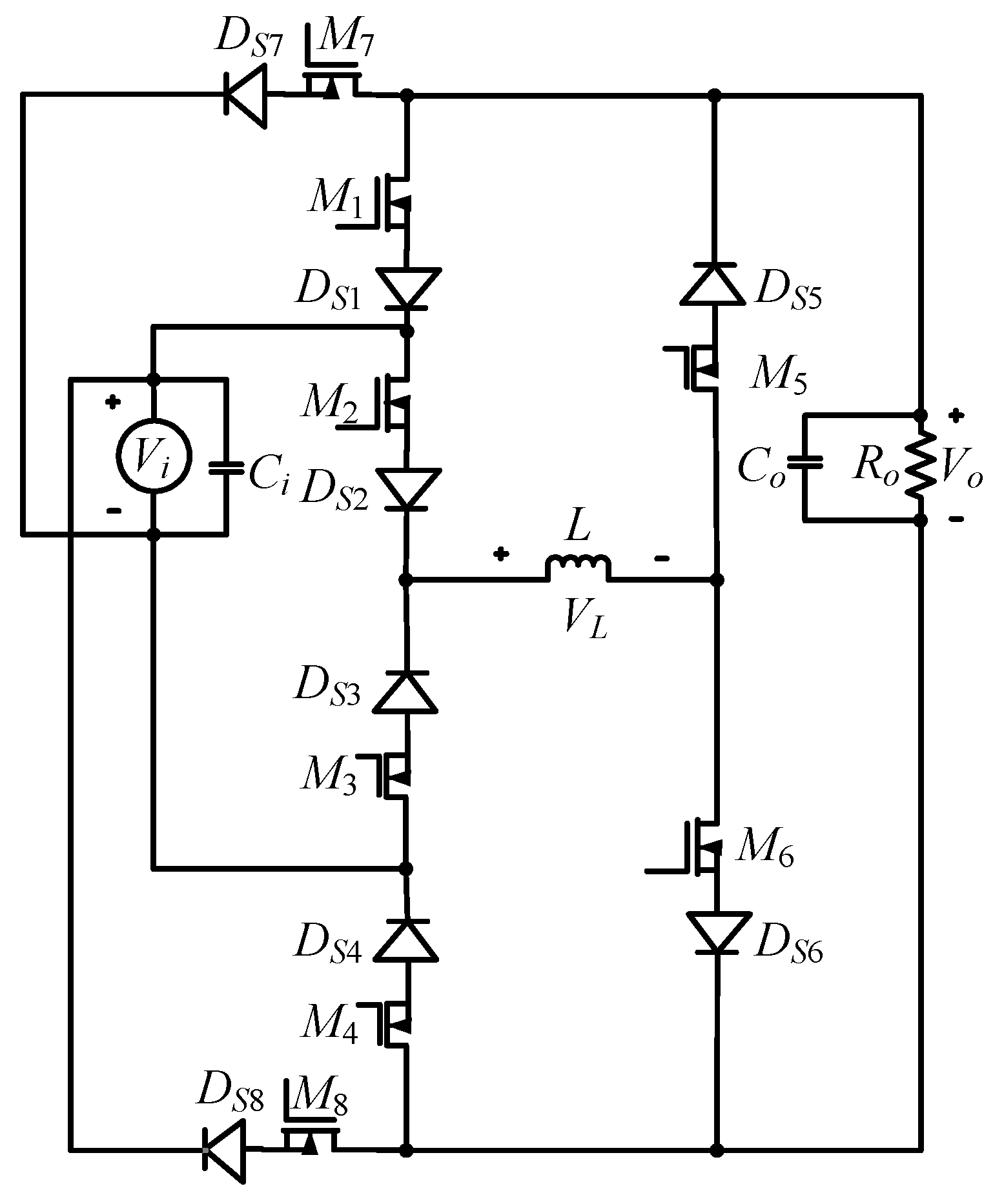
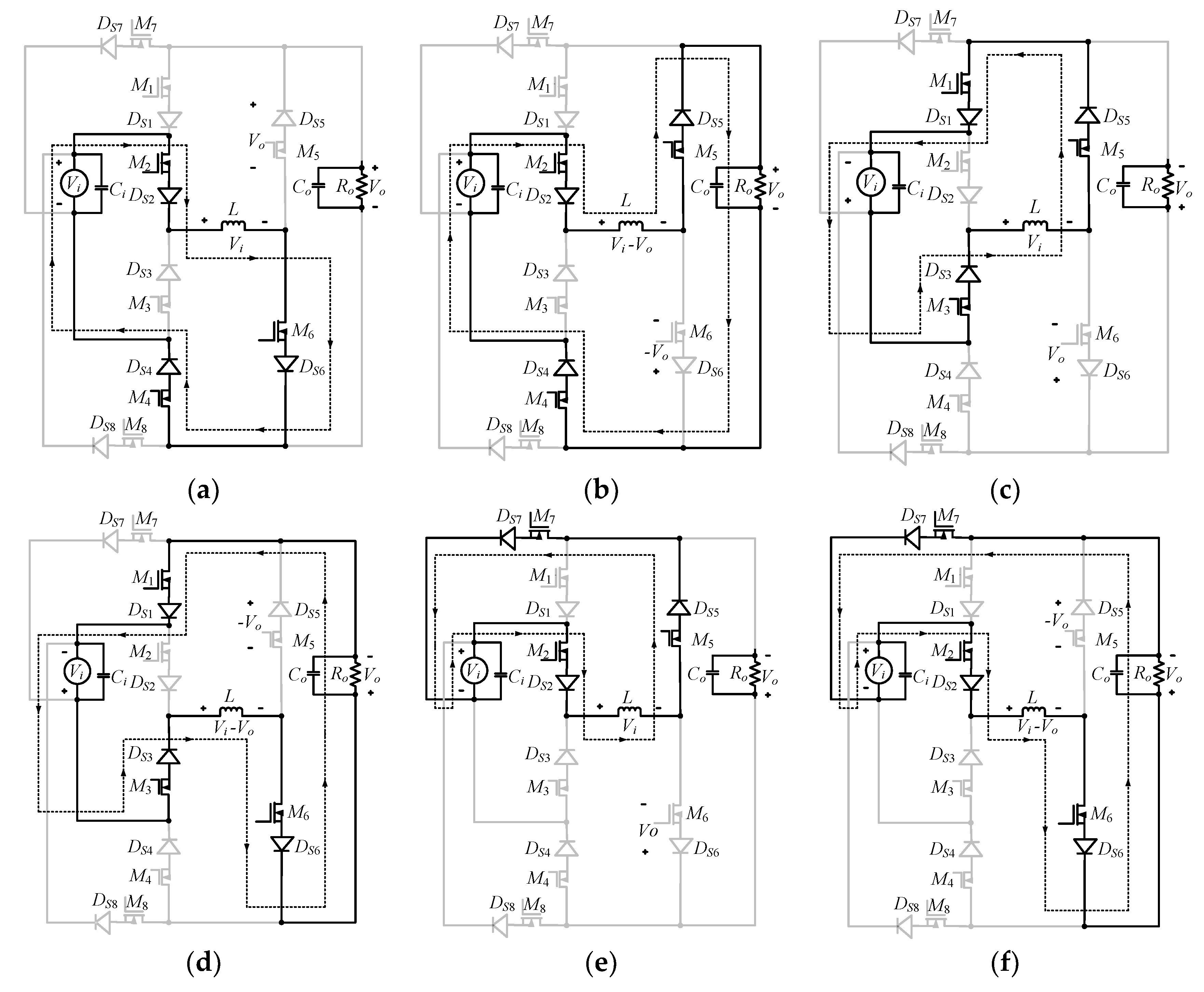
The proposed converter’s circuit consists of one filtering inductor, two capacitors, and eight MOSFET-diode series connected pairs (see
Figure 1). All its operating modes are accomplished through one high frequency DPWM control, one IDPWM control, and two low frequency switches. The remaining four switches are off throughout the operation of the converter. The DPWM switch controls the switching state of IDPWM switch. No voltage develops across the series connected diodes of DPWM control switch, due to the negative voltage at its cathode. So, the reverse voltage is developed across the MOSFET. In IDPWM control switch, as MOSFET remains in a conduction state to avoid the current interruption problem of the inductor, so its series connected diode has to withstand the reverse voltage. The proposed topology comes with the advantage that both the buck and the boost operating modes with non-inverting and inverting characteristics can be realized with the help of just changing the switching states mechanism. The series connection of diode, with MOSFET, eliminates the possible short through of input voltage, output voltage, and paralleling of input and output voltages. For example, the antiparallel arrangement of diodes
DS2,
DS3 and
DS5,
DS6, avoids the short circuiting of the input, and output voltage, respectively. In the same way,
DS1 and
DS4 avoid the paralleling of input and output voltages.
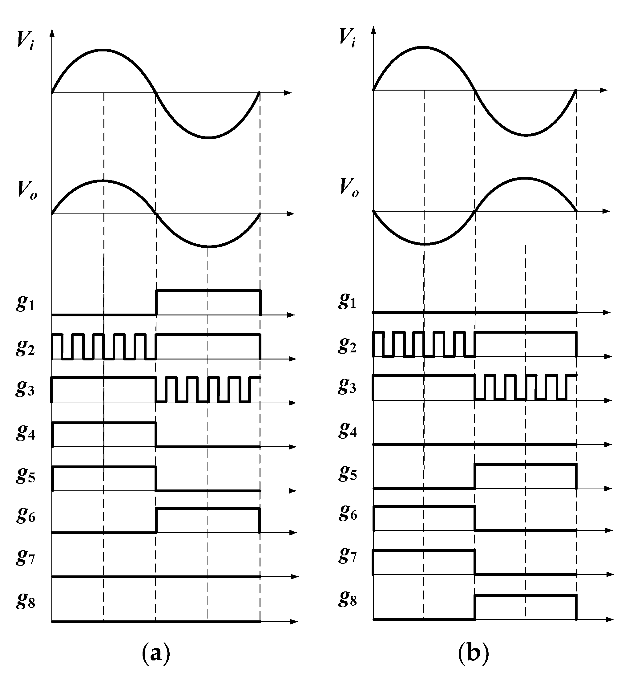
2.1. Non-Inverting and Inverting Buck Operation
The non-inverting and inverting buck operation of the suggested topology is explored in modes ‘
A’ to ‘
D’ depending upon sequence of switching signals. The voltage gain is positive and negative in non-inverting and inverting operation respectively as demonstrated in PWM scheme shown in
Figure 2. It also depicts their switching sequences for its various operating modes. For example, in non-inverting buck mode (see
Figure 2a), the switching signals
g1,
g4,
g5,
g6,
g7,
g8 and
g2,
g3 are the low, and high frequency signals, respectively. Its inverting mode may be realized only by changing the connection of the gating signals to switching devices, as depicted in
Figure 2b. The detail of its various operating modes is given below through the power transfer path.
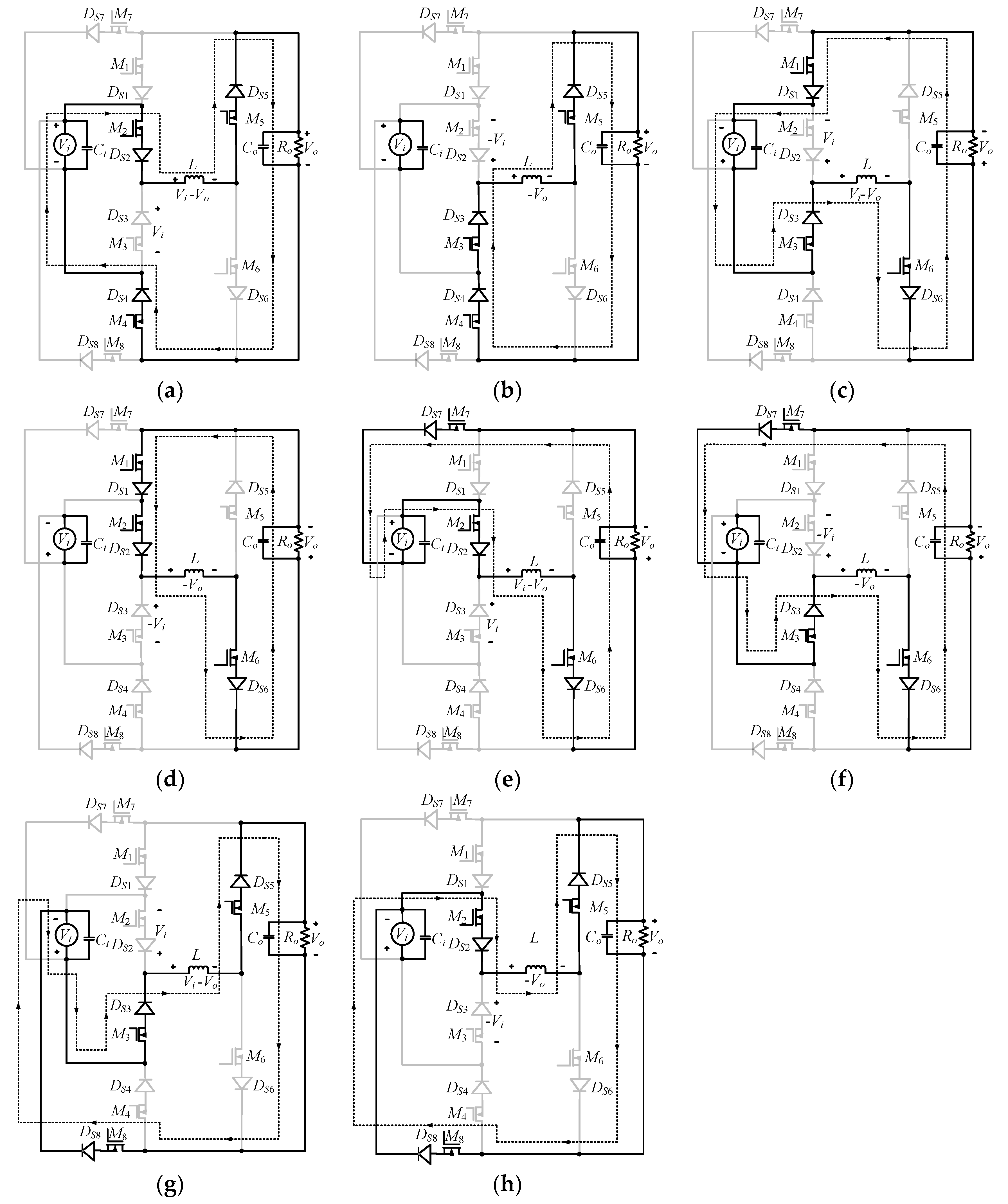
2.1.1. Operating Mode A
In mode ‘
A’, the output is non-inverted for a positive input voltage.
Figure 2a illustrates the switching signals to achieve the required target. During this operating mode, the switch
M2 is controlled in a high frequency PWM manner; the switching devices
M3,
M5,
M4,
DS2,
DS4, and
DS5 are in on-state, while
M1,
M6,
M7,
M8,
DS1,
DS6,
DS7, and
DS8 are in off-state. The controlled switch
M3 cannot conduct, due to reverse biasing of its series connected diode
DS3. During the turn-on interval of the switch
M2, the input power is delivered to load via the current conduction path, formed by the switching devices
M2,
DS2, filtering inductor
L,
M5,
DS5,
M4 and
DS4, as highlighted in
Figure 3a. In this period, the switching voltages across the DPWM and IDPWM switches are ‘0’, and ‘
Vi’, respectively. Once the switch
M2 turns off, the input power is removed from the load and the series-connected diode
DS3 becomes forward biased. The energy stored in the inductor is now supplied to load through the current conduction path of the switching devices
M3,
M5,
M4,
DS3,
DS5,
DS4, as exposed is
Figure 3b. In this period, the switching voltage of the DPWM, and IDPWM switches are changed from ‘0’, ‘
Vi’ to ‘−
Vi’, ‘0’, respectively. The dynamic state equations of inductor voltage and capacitor current are framed in Equations (1) and (2) during turn-on and -off periods of the PWM control by, applying the KVL and KCL in
Figure 3a,b as established in [
23]. The duty ratio during switching on and off intervals are represented as
d, and
, respectively.
The PWM dynamic average behavior of these state equations is obtained in Equation (3) by adding the right side of Equations (1) and (2).
2.1.2. Operating Mode B
During the negative half cycle of the input voltage, the positive voltage gain is obtained by applying the high frequency PWM control signal to switch
M3. In its on interval, the switching devices
M6,
M1,
M2,
DS6,
DS1 turn on to connect load with the source as shown in the power flow path shown in
Figure 3c. The switch
M2 remain off, as its series, connected diode
DS2 is reverse bias by the ‘
Vi’ volt. During the turn off period of its PWM control, the diode
DS2 changes it operating state from off to on as the source voltage is isolated from the load and energy stored in the inductor is delivered to load through the current flow path formed by
M1,
M2,
M6, inductor,
DS1,
DS2 and
DS6 as highlighted in
Figure 3d. The PWM dynamic averaging of this mode is developed in Equation (4) by repeating the steps of mode ‘
A’.
The voltage and current transfer ratios of mode ‘
A’ and ‘
B’ are obtained in Equation (5) by ignoring the right side of Equations (3) and (4) as they have low variation at low fundamental frequency.
2.1.3. Operating Modes C and D
Similarly, these modes are employed to have a negative voltage gain with any polarity of the input voltage. It is implemented by simply swapping the low frequency control signals
g5 with
g6, and
g4 with
g7, and
g1 with
g8, as can be investigated in its PWM modulation control, as shown in
Figure 2b. There is no change in its high frequency PWM signals,
g2 and
g3. The detail of switching and inductor voltage in these operating modes is explored with the help of power flow paths in
Figure 3e–h, for positive, and negative, input voltage, respectively. Similarly, the PWM dynamic equation, and the voltage and current transfer ratio of these operating modes are expressed in Equations (6) and (7), respectively.
The operation of the proposed converter in mode ‘A’, ‘B’ and ‘C’, ‘D’ may realize as non-inverting, and inverting, AC voltage compensator, respectively.
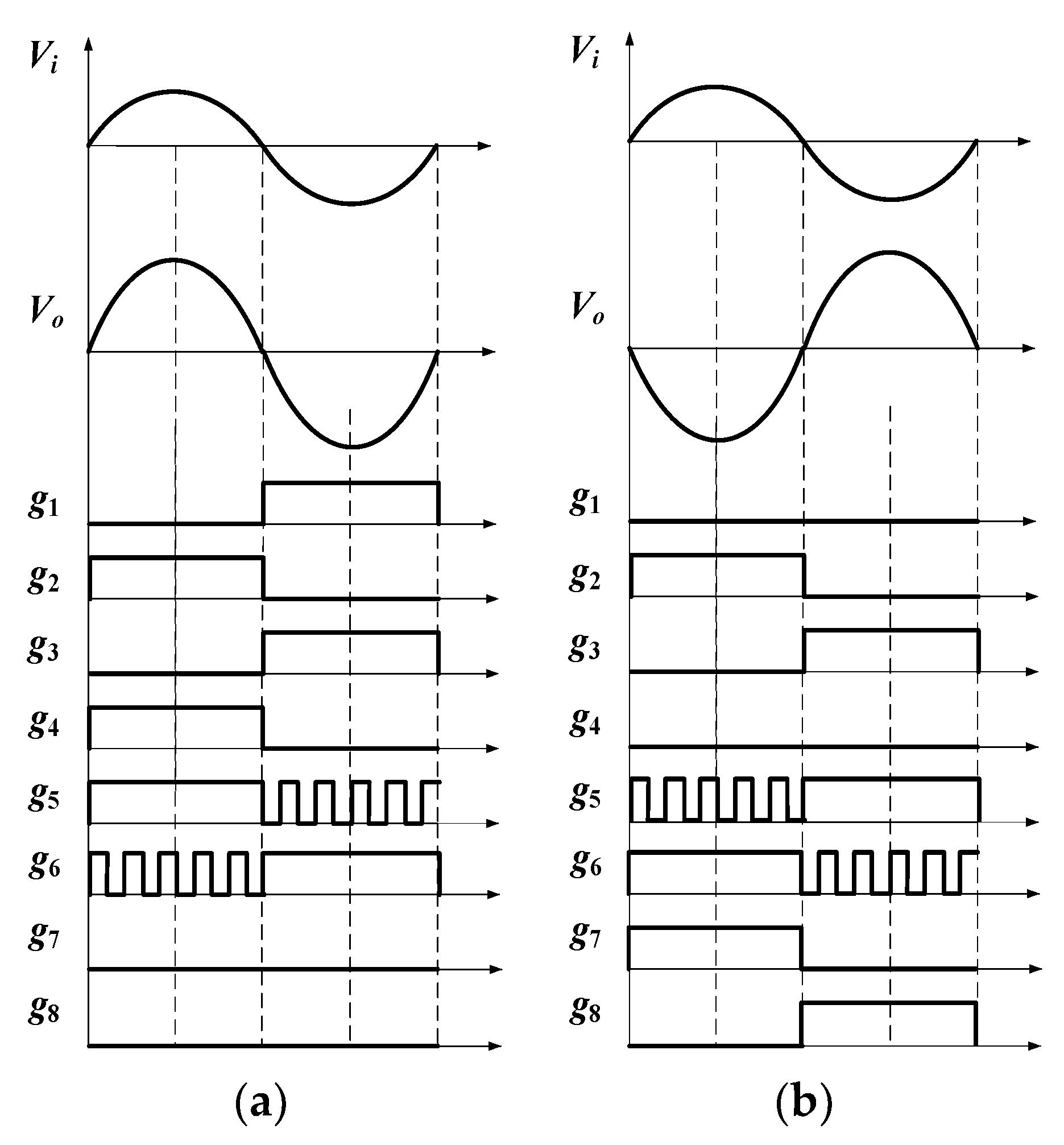
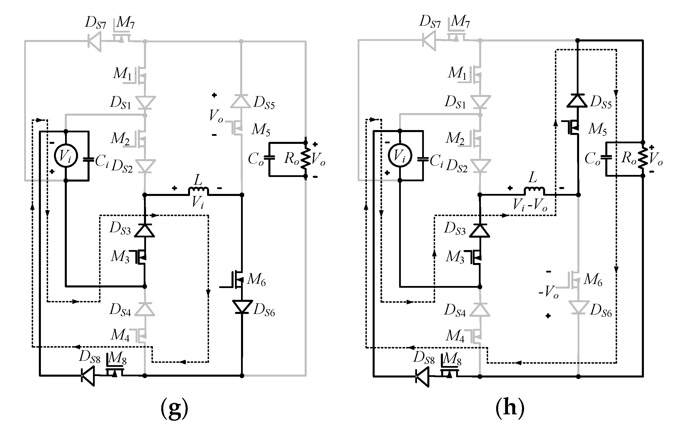
2.2. Non-Inverting and Inverting Boost Operation
The bipolar voltage gain characteristics of the proposed topology in boost operation is explored in mode ‘
E’ to ‘
F’, with respect to the polarity of the input voltage. Their PWM switching modulation strategy is shown in
Figure 4a,b for non-inverting, and inverting operation, respectively. It is clearly observed from these switching controls that boost operation can be obtained with the switching schemes, developed for the buck operation by changing the connection of the gating signals to the controlled switches. For example, the high frequency PWM signals
g2 and
g3 of non-inverting buck now become
g5, and
g6, of the none-inverting boost, respectively. The same is true for the reaming low frequency gating signals
g1,
g4,
g5, and
g6. The detail of operating modes with switching and inductor voltage, their corresponding dynamic averaging state equations, and voltage and current transfer ratio are realized in
Figure 5,
Table 1 and
Table 2 respectively.
The AC voltage controller has non-inverting and inverting boost characteristics, which may be realized by operating the suggested converter in modes ‘E’, ‘F’, and ‘G’, ‘H’, respectively. The control of duty cycle regulates their voltage gains. The input current in boost operation is inherently continuous, having low THD than that of buck or buck-boost operation.
The controlling signals of
Figure 2 and
Figure 4 depict the low control effort as only one switch at any time instant regulates the positive and negative voltage gains with buck and boost characteristics through PWM control. This control also governs the switching states of the IDPWM controlled switches indirectly as their series connected diodes become forward during the turning off periods of the DPWM switches. These switching characteristics simplify the control algorithms. The switching losses of the high frequency devices are lower at any instant of time, as only one switch is operated at low switching voltage and hence it improves the conversion efficiency.
3. Performance Evaluation with Existing Converters
The performance parameters of the proposed converter are computed to compare its performance evaluation with the existing converters in terms of voltage stresses, switching losses, inductor ripple and peak switching current as discussed below.
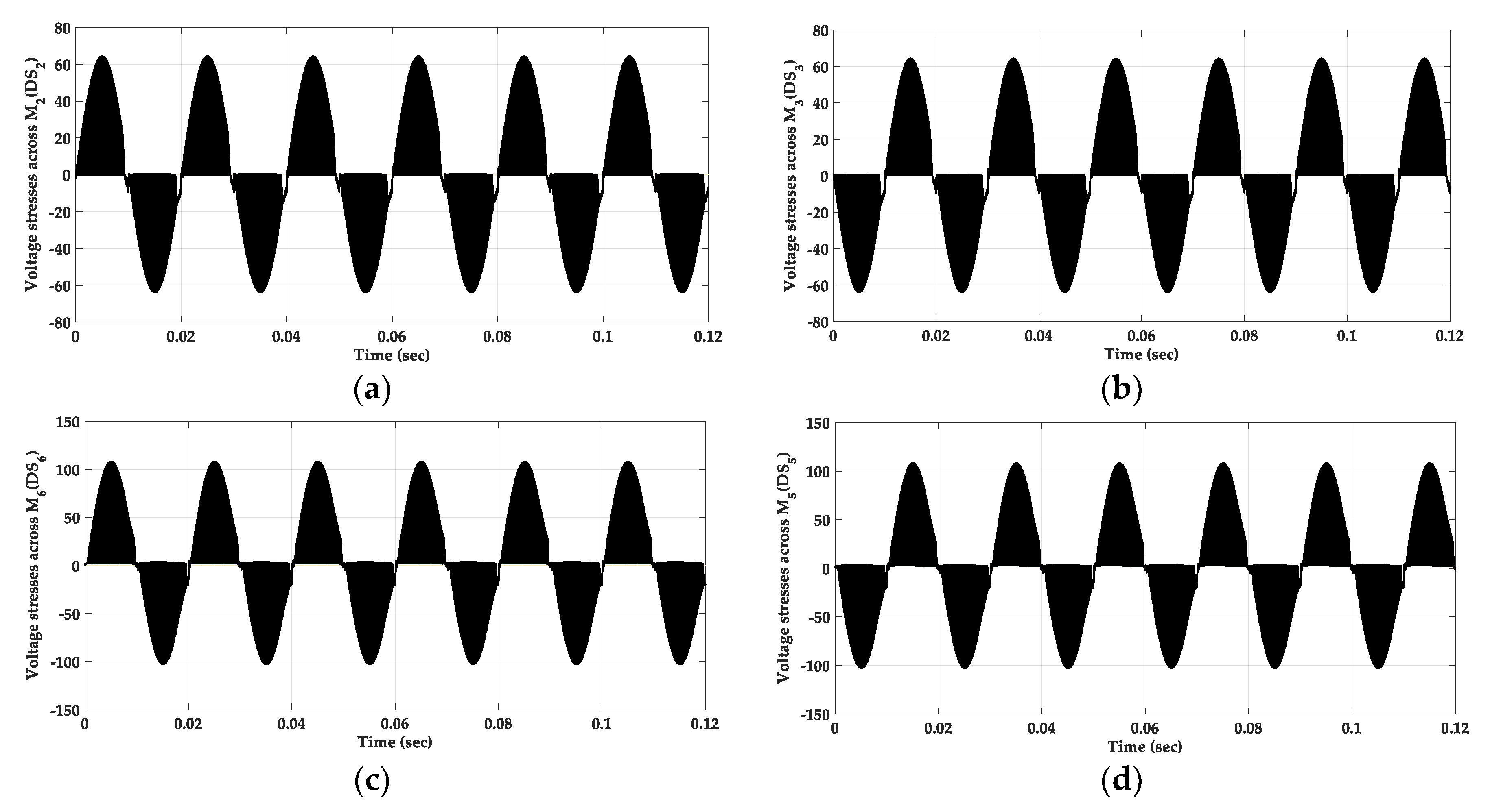
3.1. Voltage Stresses Across Switching Devices
Bipolar voltage gain in proposed converter is obtained through the high frequency switching action of
M2,
M3 for buck and
M5,
M6 for boost operation. The peak switching voltage across the high frequency-controlled switches operating in non-inverting and inverting buck and boost are given in Equation (8).
Similarly, the maximum voltage stresses of the high frequency-controlled switches in inverting buck-boost mode of [
22] are computed in Equation (9).
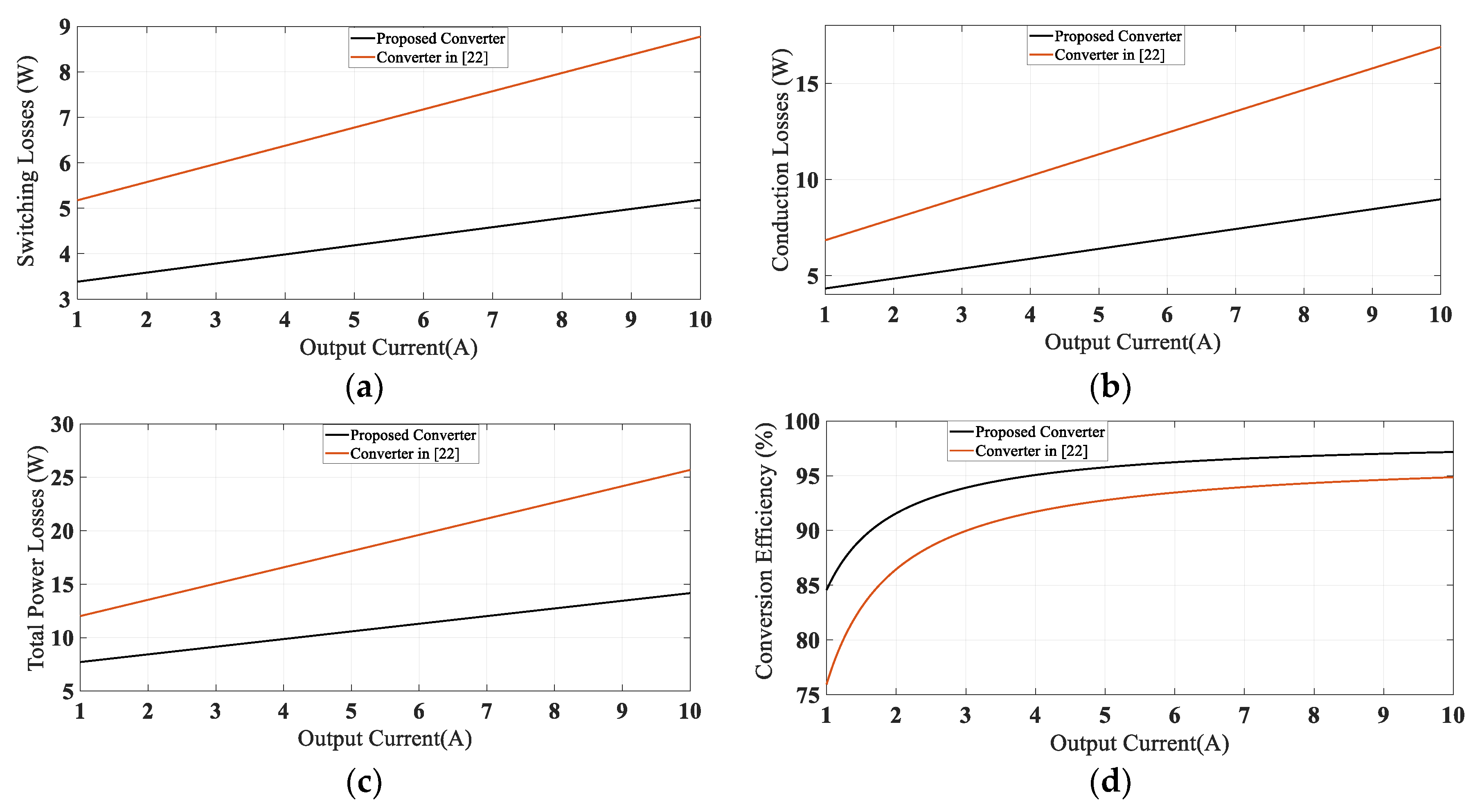
As can be seen from Equations (8) and (9) that the proposed converter has 50% low switching stresses with voltage gain of 0.5 and 2 for inverting buck and boost mode respectively. So, the proposed converter has low voltage rating, low dv/dt problem and low switching losses.
3.2. Inductor Ripple and Switching Currents
The comparison of inductor ripple and switching currents is carried for the voltage gain of 0.5 and 2 for buck and boost mode respectively.
The analysis and comparison from Equations (10) to (13) explores that the proposed converter has low inductor ripple and switching current having low conduction losses and low losses in the DCR resistance of filtering inductor. These losses are proportional to the magnitude of the conducting currents. They also depend on their internal resistances and forward voltage drops. Low switching voltage devices have low on-state resistances and forward voltage drops. The proposed topology has low conduction losses due to low conduction current and switching voltage as can be observed from Equations (10) to (13). The quality of the output voltage depends on the ripple voltage that is improved due to low inductor ripple current. In addition, during the short through intervals, the output is distorted. Therefore, absence of short through problem and low ripples improve the power quality of the output voltage.
3.3. Switching Losses
The switching losses of a MOSFET depend on switching voltage, current, switching frequency, output capacitance, rise and fall time as reported in [
23]. These losses in fast recovery diode depend on its reverse recovery characteristics as in [
23]. They are also proportional to number of high-frequency switching devices and voltage gain. The switching losses of DPWM control switch only come from the switching of MOSFET as its series connected diode is forward biased due to negative reverse voltage. The switching losses of IDPWM controlled switch are only due to reverse biasing of diode as MOSFET is kept turned on to ensure the continuous conduction of inductor current.
The buck operation of the proposed circuit is implemented with high frequency PWM control of
M2(
M3) and
DS2(
DS3). The total switching losses of the proposed converter and the converter in [
22] in inverting mode are computed by assuming same switching current and constant input voltage in Equations (14) and (15) respectively.
where
fsw is switching frequency,
IL is the switching current,
Cos is output capacitance of MOSFET,
QRR is the reverse recovery charge of series connected fast recovery diode,
Vi is the input voltages, and
GV is the voltage gain. The proposed converter has 50% low switching losses than that of converter in [
22] during buck and boost operation with voltage gain of 0.5 and 2 respectively.
3.4. Conduction Losses
The conduction losses of a MOSFET-diode pair depend on their forward voltages and resistances. They also depend on their conduction currents. The conduction losses of the proposed topology and converter in [
22] are realized in Equations (16) and (17) for voltage gain of ‘2’ respectively, where
RT and
Rd are on-state resistances of MOSFET and diode respectively whereas
Vd is the forward voltage of the diode.
The above comparison depicts that the proposed topology has low conduction losses.
In a summary, the comparison of the proposed topology with the existing converter in [
22] is detailed in
Table 3 and
Table 4 for buck and boost mode respectively. For the sake of making comparison simple, terms involving
Cos are neglected.
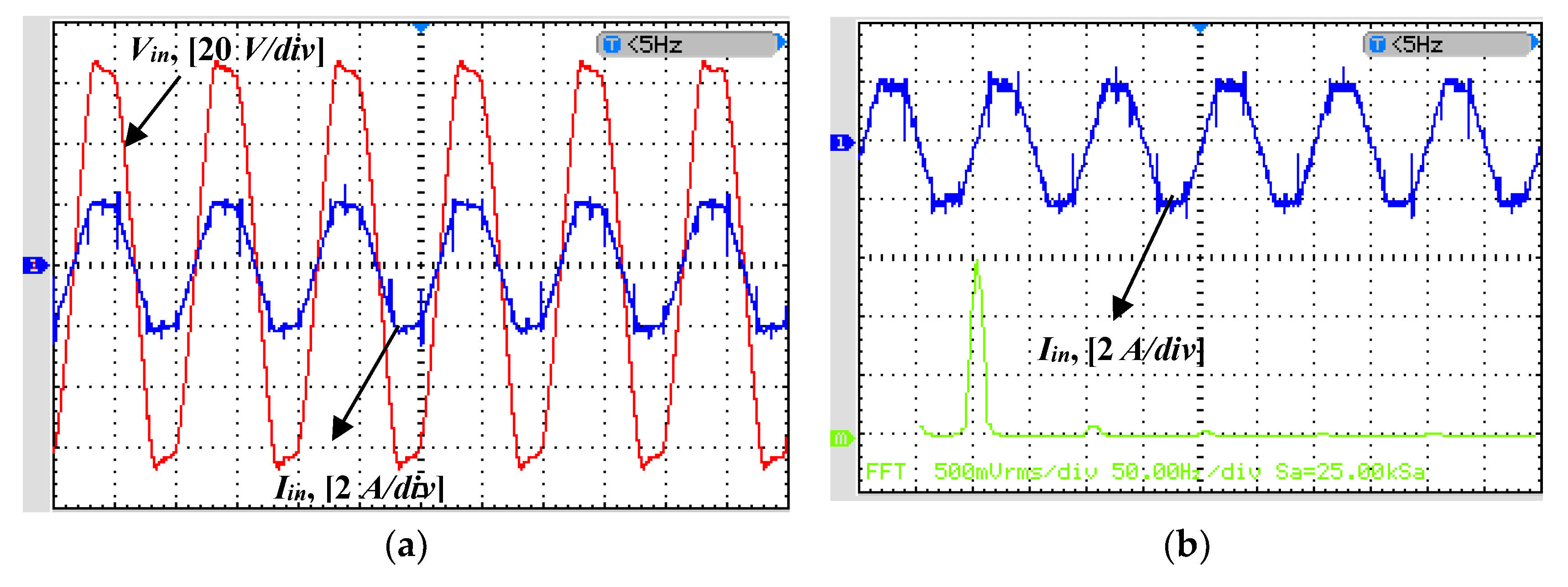
6. Conclusions
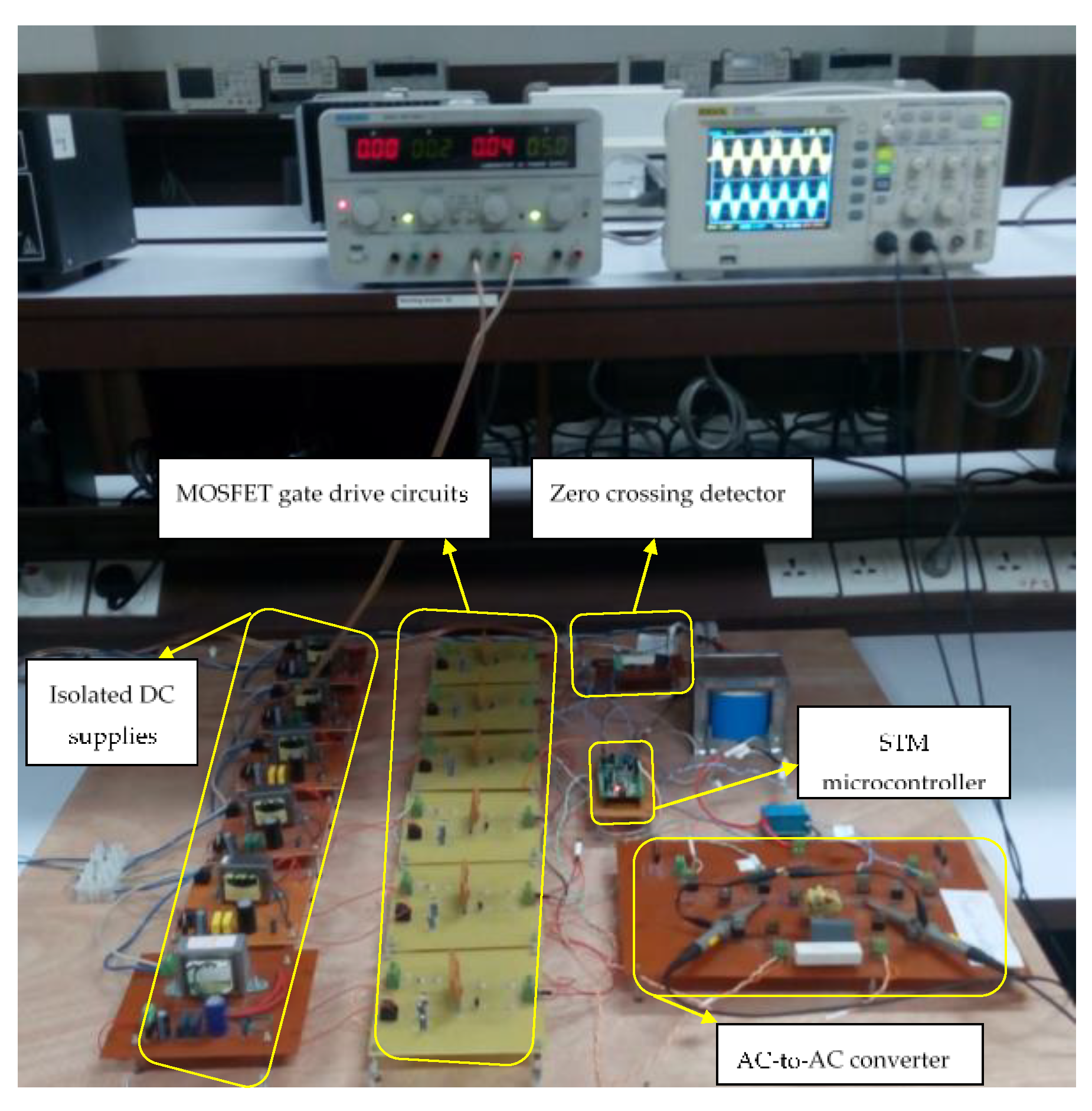
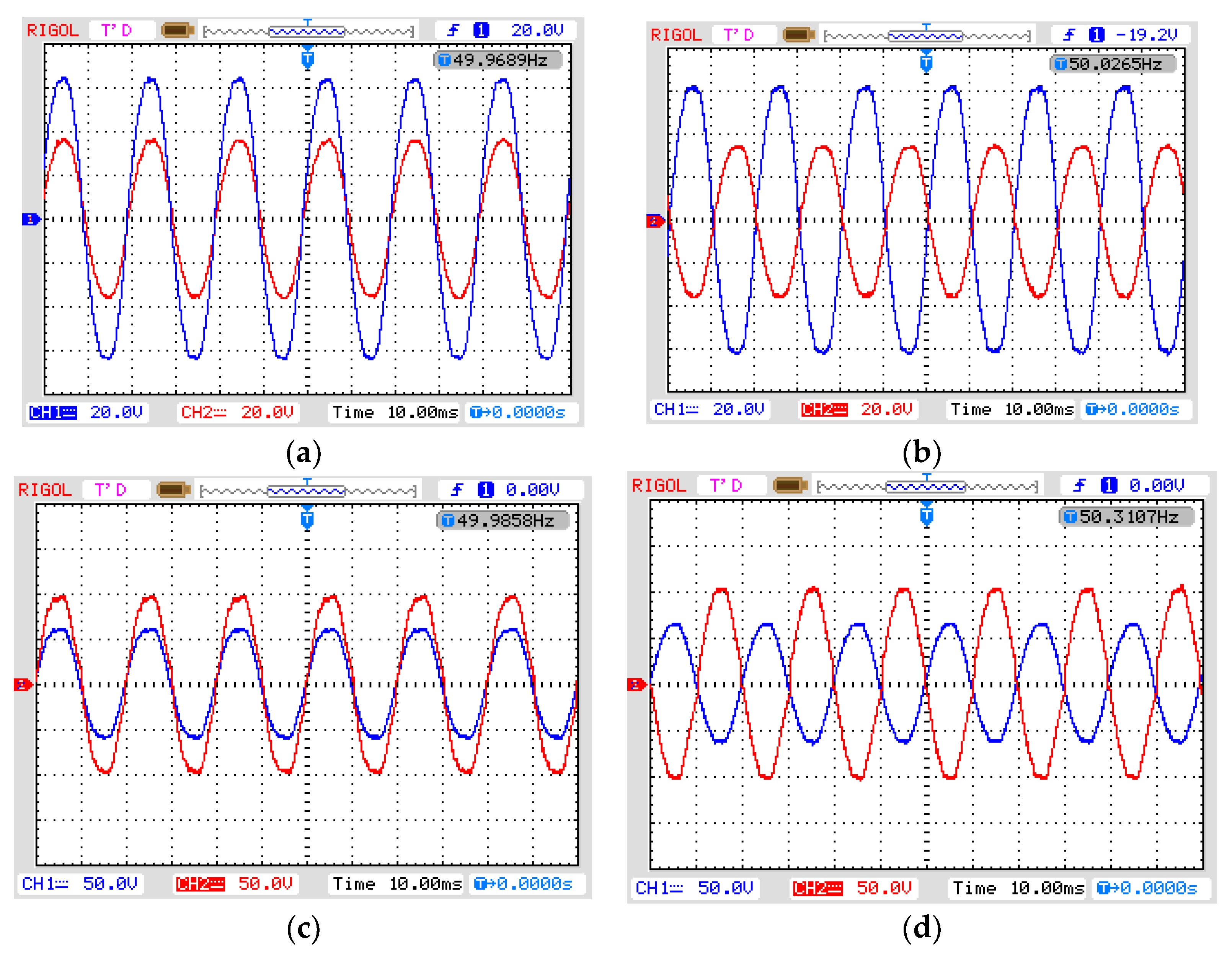
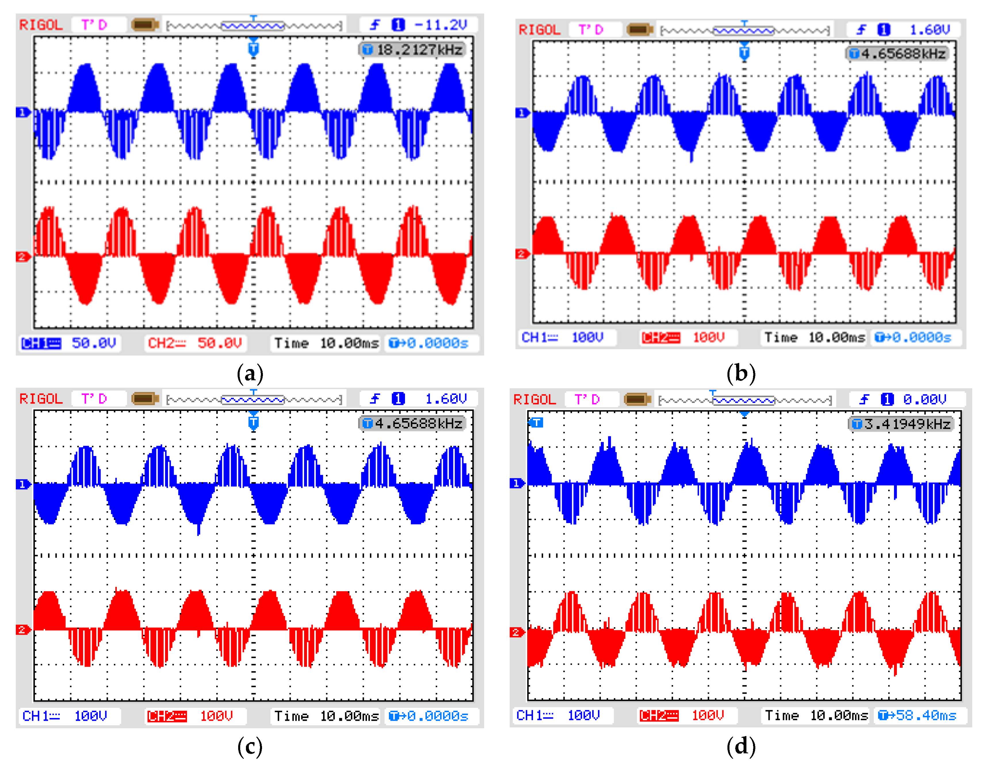
A novel AC voltage controller, operating in separate buck and boost mode, with a bipolar voltage gain, is proposed in this research. In all operating modes of the proposed topology, the voltage stresses across the high frequency switches, are reduced to 50%, with the duty ratio of 0.5. The high switching frequency control effort is also reduced by implementing all operating modes with one DPWM and one IDPWM control switch. Each operating mode requires the conduction of two low frequency switches having a low internal resistance and forward voltage. The proposed topology, not only offers less voltage stresses across the high frequency switches but also reduced peak inductor ripple current, peak switching device current, and conversion losses (switching and conduction power losses), thus improved efficiency compared to the other topology reported in literature. The devices with low voltage and current ratings can be utilized, due to the reduced voltage stresses. A low ripple in the output voltage and the absence of short through issues, improve the power quality of the output voltage. The hardware implementation of the proposed converter validates the simulation results obtained in the MATLAB/Simulink environment.

 ,
, 


