A Driving Technique for AC-AC Direct Matrix Converters Based on Sigma-Delta Modulation †


DII—Dipartimento di Ingegneria dell’Informazione, Università Politecnica delle Marche, Via Brecce Bianche 12, I-60131 Ancona, Italy
*
Author to whom correspondence should be addressed.
†
This paper is an extended version of our paper published in EEEIC 2018—18th International Conference on Environment and Electrical Engineering.
Energies 2019, 12(6), 1103; https://doi.org/10.3390/en12061103
Submission received: 14 January 2019
/
Revised: 14 March 2019
/
Accepted: 15 March 2019
/
Published: 21 March 2019
(This article belongs to the Special Issue Selected Papers from EEEIC 2018—18th International Conference on Environment and Electrical Engineering)
Abstract
:Direct conversion of AC power between three-phase systems operating at different frequencies can be achieved using solid-state circuits known as matrix converters. These converters do not need energy storage elements, but they require sophisticated control algorithms to operate the switches. In this work we propose and evaluate the use of a sigma-delta modulation approach to control the operation of a direct matrix converter, together with a revised line filter topology suited to better handle the peculiarities of the switching noise produced by the sigma-delta modulation. Simulation results show the feasibility of such an approach, which is able to generate arbitrary output waveforms and adjust its input reactive power. Comparison with a space vector modulation implementation shows also better performance about total harmonic distortion, i.e., less harmonics in the input and output.
1. Introduction
Matrix converters are forced commutated converters that have the desirable property of a simple and compact circuitry, based on a matrix of bidirectional switches. This configuration allows direct conversion of energy from a three-phase AC source to another three-phase AC system, operating at a different voltage and frequency, without needing a DC link with the function of energy reservoir. The absence of a DC link also dispenses with its related energy storage components, such as inductors and capacitors.
A DC link can indeed be present in a category of converters called indirect matrix, which are composed of two distinct groups of switches: a group is connected to the line, and has a similar function to that of a rectifier, the other is connected to the load, and acts as an inverter, but they work without the reservoir capacitor on the DC bus. In the direct matrix converter, on the other hand, there is no DC link at all and an array of nine switches is able to directly connect any of the load phases with any of the line phases to provide the desired conversion.
Both these kinds of AC-AC converters share most of the same desirable properties, such as high reliability due to the absence of critical capacitors or inductors, adjustable amplitude and frequency of the load voltage, sinusoidal input and output currents, and can also provide reactive power to the line by presenting an arbitrarily adjustable input power factor [1].
Thus their interest has more and more increased in recent years for their possible applications on industrial fields such as avionics [2,3], green energy systems such as wind and photovoltaic systems [4,5,6], marine propulsion [7], geophysics [8], electric vehicles [9], and smart cities [10].
Literature reports different control schemes, such as Alesina-Venturini method [11,12] and space vector modulation (SVM) techniques [13,14]. The Alesina-Venturini method [11,12], also known as direct transfer function approach, introduced the concept of low-frequency modulation matrix. Multiplying the input voltages by this modulation index produces the output voltages.
The other, perhaps more widely adopted, algorithm to control matrix converters is the SVM. At first, SVM was defined to control indirect matrices [13] through the concept of fictitious DC link. Originally it was devised to control the load voltage [15] alone, but was then extended so that it can also correct the input power factor. Its modulation performance was also improved [16]. Recently, another SVM method has been proposed [14], that uses the concept of instantaneous space vector to represent voltages and currents, both at the input and output, and is not limited to indirect matrix converters.
In this work we present a matrix control algorithm based on sigma-delta () modulation. modulation exploits oversampling and noise shaping to spread quantization noise, so that it occupies a much larger band than the band occupied by the signal, easing the removal of this noise by an analog filter. Noise shaping is performed by a digital filter in the control loop that further reduces the noise in the signal band, at the cost of increasing it at frequencies much higher than those in the signal band. modulators are routinely employed in the field of analog to digital conversion [17] and have also found application in the control of switch-mode power supplies [18] and LED drivers [19].
This paper proposes the use a modulation method to operate a matrix converter, where the operation of the switch matrix is seen as the source of the quantization noise, whose spectrum the modulator seeks to shape so that it can be easily filtered out [20]. Compared to a standard pulse width modulation (PWM), modulation also considers, and then compensates by virtue of its digital filter acting like an integrator, the past quantization errors performed by the switch matrix. Compared to an SVM implementation, the approach is conceptually much simpler and is amenable to a straightforward implementation. Moreover, the quantizer can use all of the 27 possible combinations provided by the switches, providing finer granularity of the output voltage selection, not being limited like SVM to those that provide output space vectors with fixed directions. The peculiarities of the quantization (switching) noise produced by this modulator will also be discussed and investigated, together with a novel filter topology that takes into account the particular frequency distribution of the quantization error.
This paper is organized as follows. Section 2 discusses the theory on which is based by extending its traditional application to include the operation of a direct matrix converter, and discusses the novel line and load filters. Section 3 presents the results of some simulation experiments to validate the operation and effectiveness of the proposed approach, comparing it with the conventional SVM method. Section 4 finally ends the work.
2. Theory and Methods
In this section, the sigma-delta based modulation technique used to control the switch matrix is presented and discussed. For reference, a direct matrix converter, with no DC link, will be considered, though the basic idea can easily be applied to indirect converters as well.
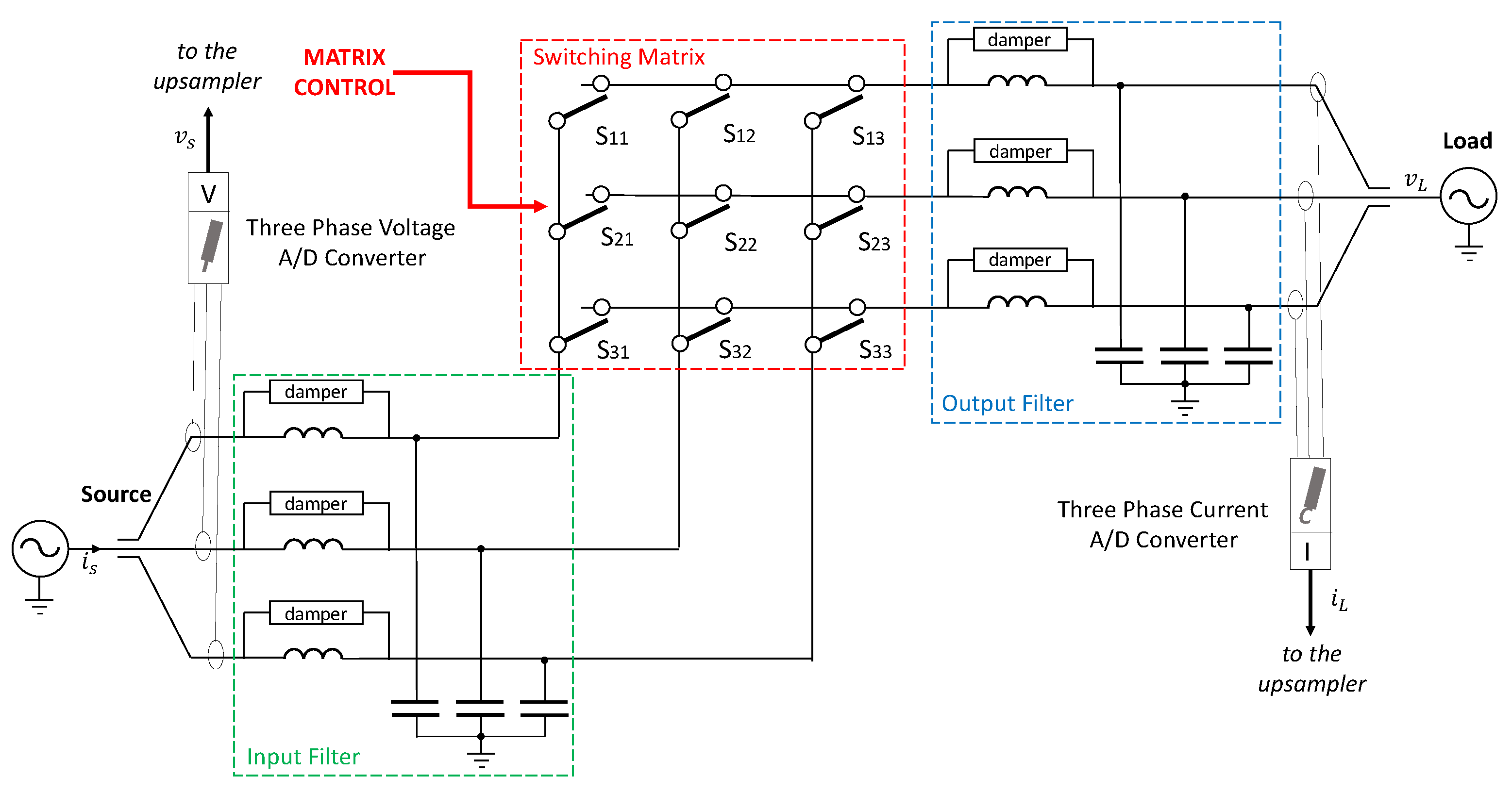
The main components of a direct matrix converter, as shown in Figure 1, are the three-phase voltage source, an input filter, the matrix of switches, an output filter, and the load. In order to properly control the switches, it is necessary to sample at least the source voltage and the load current.
Let be the vector of instantaneous voltages of the three-phase system at the switching matrix input, and be the vector of instantaneous voltages at the output of said switching matrix.
The voltage transfer function of a direct matrix converter coincides with its incidence matrix , that is, a matrix whose element is 1 if the switch connecting the input phase j to the output phase i is on, 0 otherwise. The current transfer function is just the transpose of said incidence matrix, that is,
with spanning all the admissible configurations of the switch matrix. To avoid input phase short circuits, under no circumstances can two switches on the same row be activated simultaneously, hence the incidence matrix must be subjected to the following restriction
With this limitation, the number of different incidence matrices is just .
The three-phase power supply is assumed to generate the following instantaneous phase voltages
with and . The line-to-line voltages will then be
Similarly, the desired output voltages are
where is the initial phase difference between input and output voltages, while and are the desired output frequency and root mean square (RMS) voltage, respectively.
2.1. Sigma-Delta Modulation
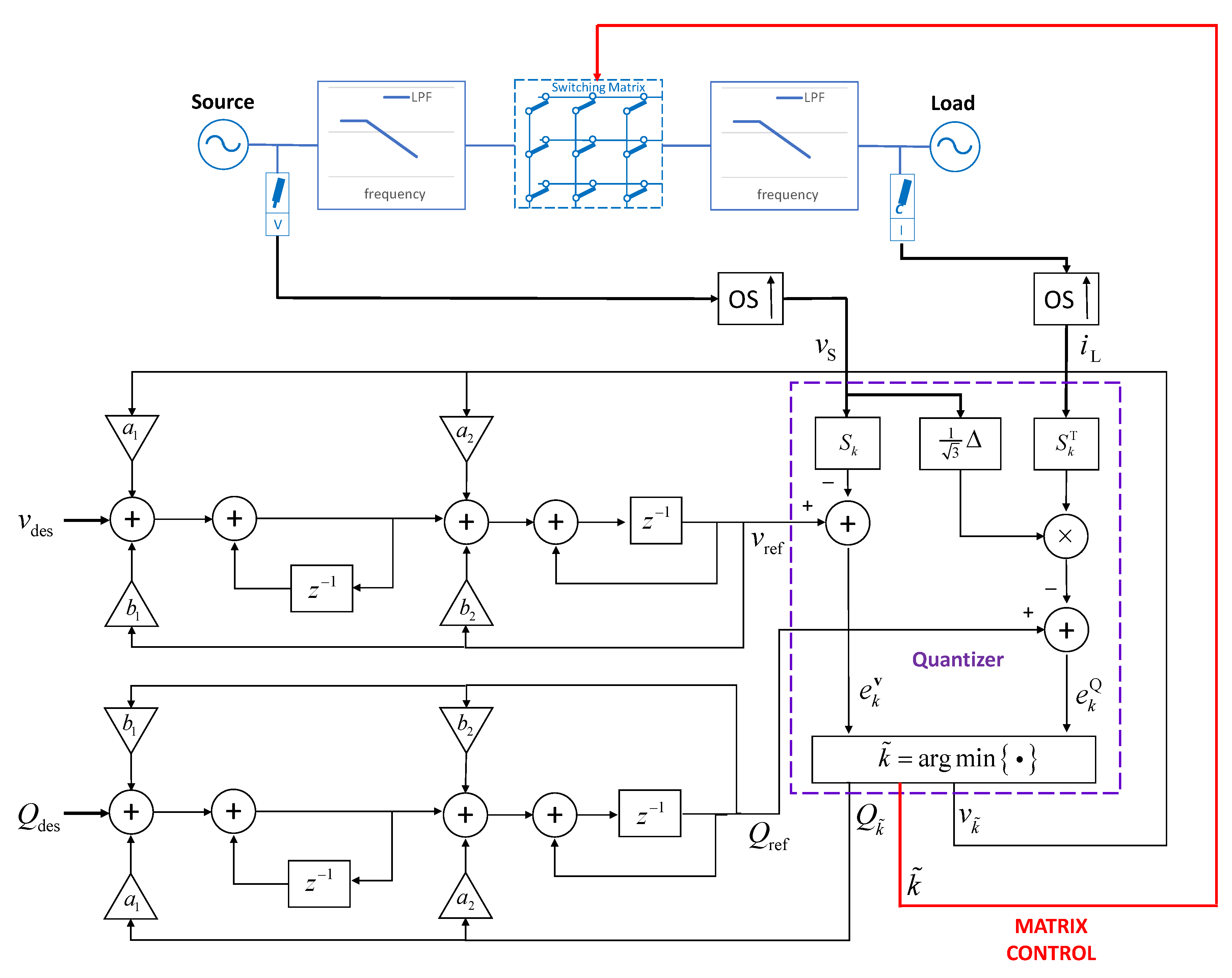
The sigma-delta modulator is a digital circuit, shown in Figure 2 together with a simplified block diagram of the power stages already presented in Figure 1. The two “OS↑” frequency upsampler blocks are needed to adjust sampling rates as the digital portion of the modulator typically uses a higher clock frequency than the AD converters. Its main principle of operation is to use samples of the source voltage and of the load current to compute the best switch configuration to apply to the matrix to achieve the desired result, namely, the desired output voltage and input reactive power .
It is composed of a noise-shaping filter (shown on the left of the figure) that computes the reference signals and from the desired output and the previously occurred quantization errors, and of a quantizer that chooses the best output to approximate said references from the the noise-shaping filter outputs and an oversampled version of the source voltage, , and load current .
It operates as follows. Let us call , with , the output voltages the quantizer can produce. Usually, a conventional sigma-delta modulator employs a quantizer with fixed quantization levels. In our case, these levels are determined by the different configurations of the switch matrix, and are hence time varying as the input voltage and output current evolve in time. The quantizer thus needs to update its knowledge of the available levels by multiplying the sampled input and output quantities by all the 27 possible matrices , so that .
Nevertheless, since these quantities are relatively slowly time varying, with respect to the clock frequency , a low sampling frequency can be employed and the signals interpolated when needed.
The noise-shaping filter then ensures that the time average of the output voltage be equal to the desired voltage , by taking into consideration past quantization errors and computing the required correction that need to be applied next to compensate for them, as
where STF is the modulator linearized signal transfer function, and NTF is the quantization noise transfer function. These functions must be designed so that the STF does not distort the input signal, while the NTF should place most of the noise at high frequencies where it can easily be attenuated by the line and load filters.
The quantizer must then find the most appropriate output level to simultaneously achieve both objectives. This can be done by minimizing an objective function that is a linear combination of two functionals, one proportional to the errors on the output voltage, and one proportional to the error in the input reactive power.
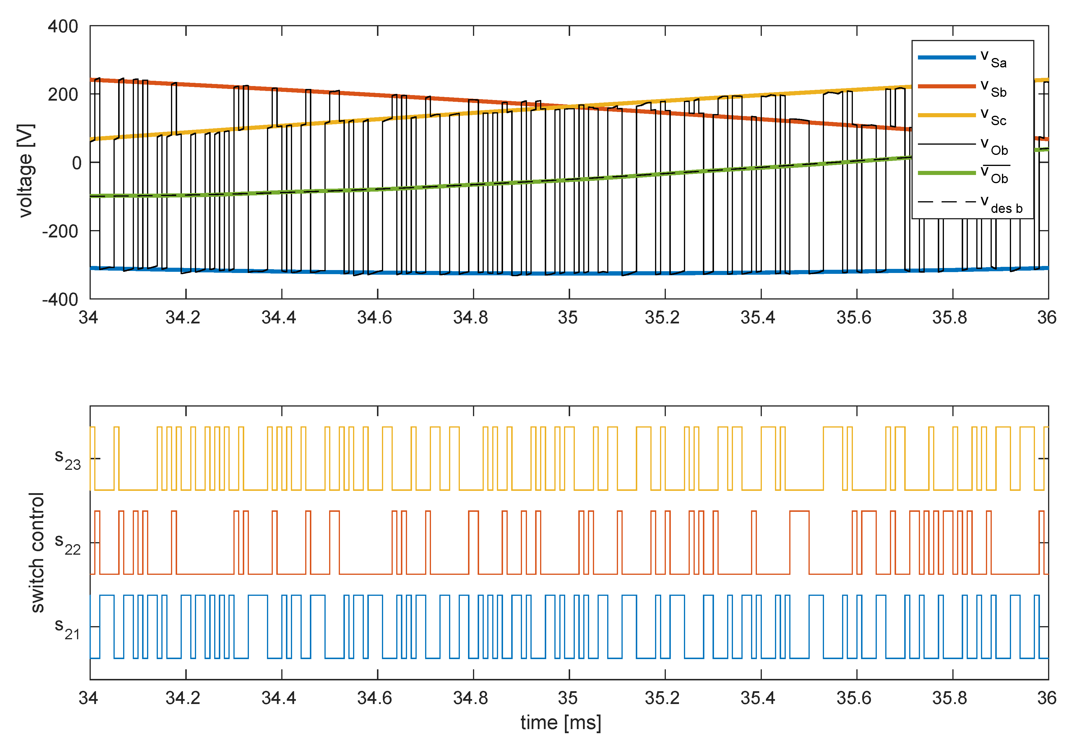
Before detailing its operation in the following, Figure 3 shows an example of the switching sequence produced by such modulator for one output phase for a short time frame. Due to the constraint (3), each output phase must be connected to one and only one input phase at any given time. Hence, the available voltage levels are those of the input phases , which in the time span considered are quite slowly time varying. The modulator needs to approximate by switching between the three available levels (, thin black line) so that the averaged output matches the desired output.
Since the modulator operates in the discrete time domain, in the following we will assume sampled signals with , and derive expressions for the errors as functions of the index k that describes the configuration of the switches.
2.1.1. Noise Shaping Filter
The structure of the noise-shaping filter used in the modulator is shown in Figure 2.
The linearized signal transfer function and quantization noise transfer function of the modulator are
where the and coefficients are those shown in Figure 2.
The poles of both transfer functions, that share the same denominator, can be placed at infinite so that the STF becomes simply a delay. This can be achieved by ensuring that
so that the signal is not influenced by the filter. The NTF zeros can be placed either in DC or within the signal band to minimize the in-band noise. We chose to put them at to minimize the amount of noise near the filter resonances. They will thus be placed in the unitary circle at
where is the zero’s frequency normalized with respect to the Nyquist frequency. To ensure this it must be
which, together with the constraints on the poles, yields
which can be used to implement the digital filter.
2.1.2. Output Voltage Error
Since is a low-pass filtered version of , the aim of the modulator is to make on average equal to , so that . The noise-shaping filter provides the best estimate of the voltage needed to achieve this objective. At each time n the quantizer must then choose the configuration , to be applied at the next step, that minimizes
where .
By rewriting (1) in the discrete time domain, we have
Furthermore, since the aim of the input filter is to suppress high-frequency current components, and not to alter the line voltages, can be approximated as , and the difference between the values at time and n can be neglected since , so that . We can thus write
The above approximation lets us write
so that the error can be computed from the measured voltage .
2.1.3. Input Reactive Power Error
The instantaneous reactive power [21] at the input of the switch matrix can be written as , where “” denotes the scalar product. Under the hypothesis , it is thus
where can be computed from the measured output current, transformed by the matrix function (2), so that
where we have used the fact that both and are slowly varying with respect to , and that the output filter should ensure , to make computable from the measured quantities.
Let us then define the error on matrix input reactive power as
where is the needed reactive power to obtain the desired , as computed by the noise-shaping filter.
In order for the reactive power to be null at the source, the reactive power at the matrix input should be the opposite of that created by the input filter, which manifest a strong capacitive load at line frequency as the filter main capacitors experiment the entire three-phase supply voltage. We can thus assume
2.1.4. Multi-Objective Optimization
To find the best quantization level that simultaneously minimizes both errors, it is useful to normalize them so that they can be combined. The error (23) can be normalized with respect to the input and output voltages to get the adimensional error
while the error (26) can then be normalized as
The normalized errors (28) and (29) are combined to find the solution to this multi-objective optimization problem. This can be achieved by choosing the point of the Pareto frontier, lying in the space of the two normalized errors, that happen to be closer to the origin, such as
so that the matrix configuration that minimizes the functional in (30) is chosen as the next step.
2.2. Input and Output Filters
Generally, to reduce the effect of voltage and current switching, an LC filter is used at the input and output of the matrix converter. For the sake of simplicity, we will focus on a single-phase filter, like the one shown in Figure 4.
For our purposes it can usefully be represented with the inverse hybrid representation
The problem with this filter is that, although losses are generally required to avoid producing strong harmonics at the resonance frequency, these losses are present across a very large portion of the frequency spectrum, thus causing serious efficiency degradation if the switching noise is spread over a large bandwidth, as is the case with sigma-delta modulation.
In fact, the power lost in the filter can be computed as , which, using (31), becomes for the three-phase case
where it is worth noticing that, if voltage and current are in phase, the term equals 0.
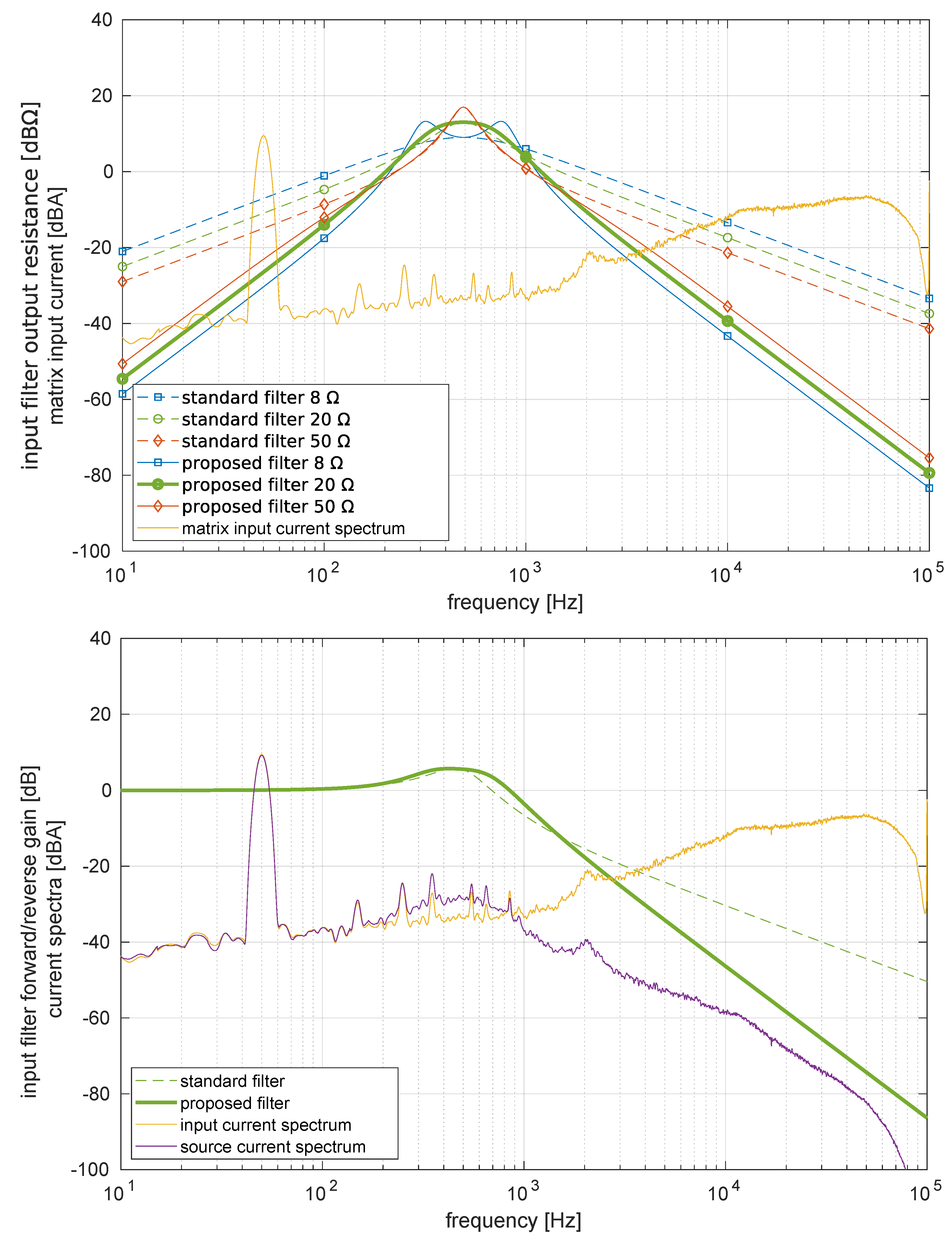
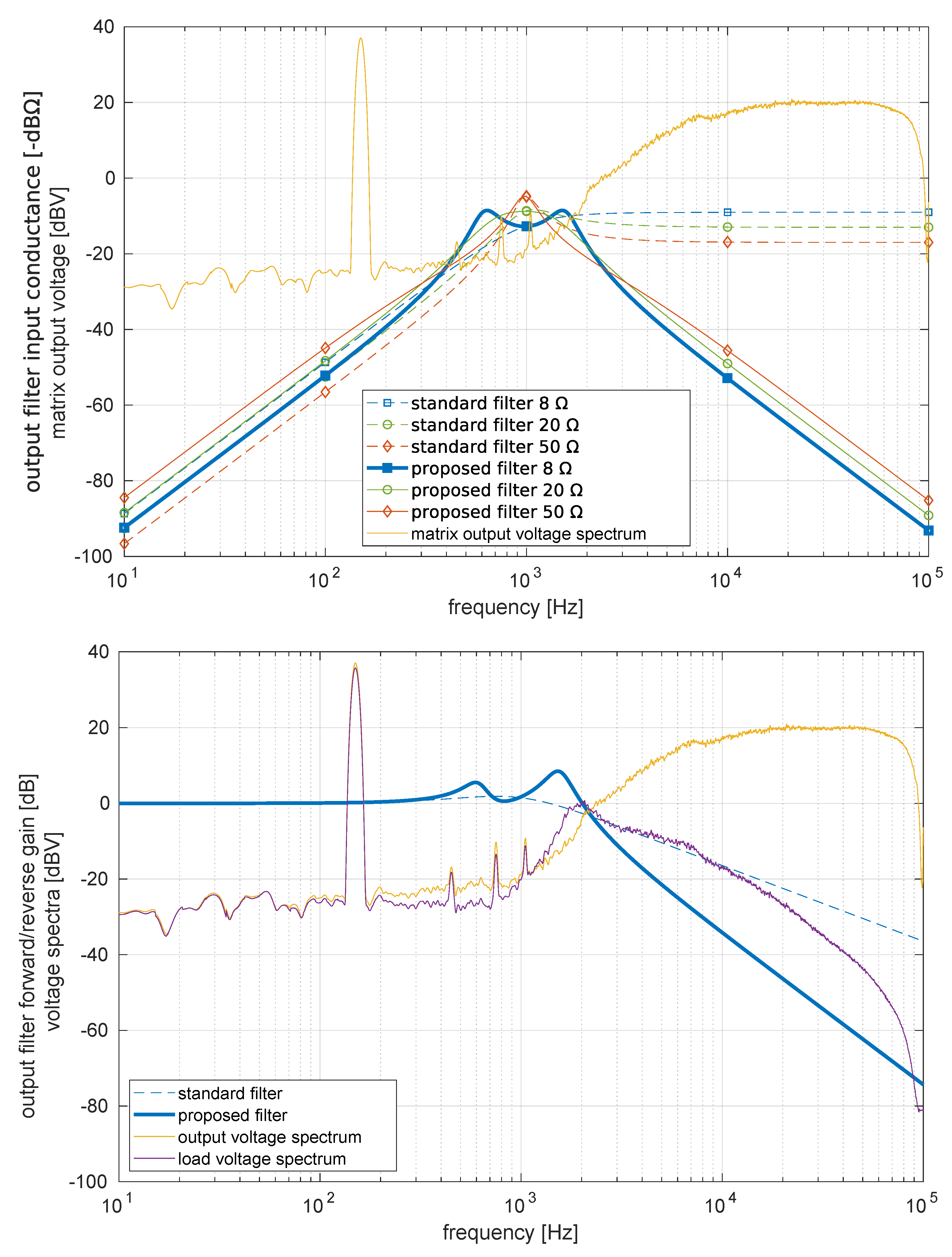
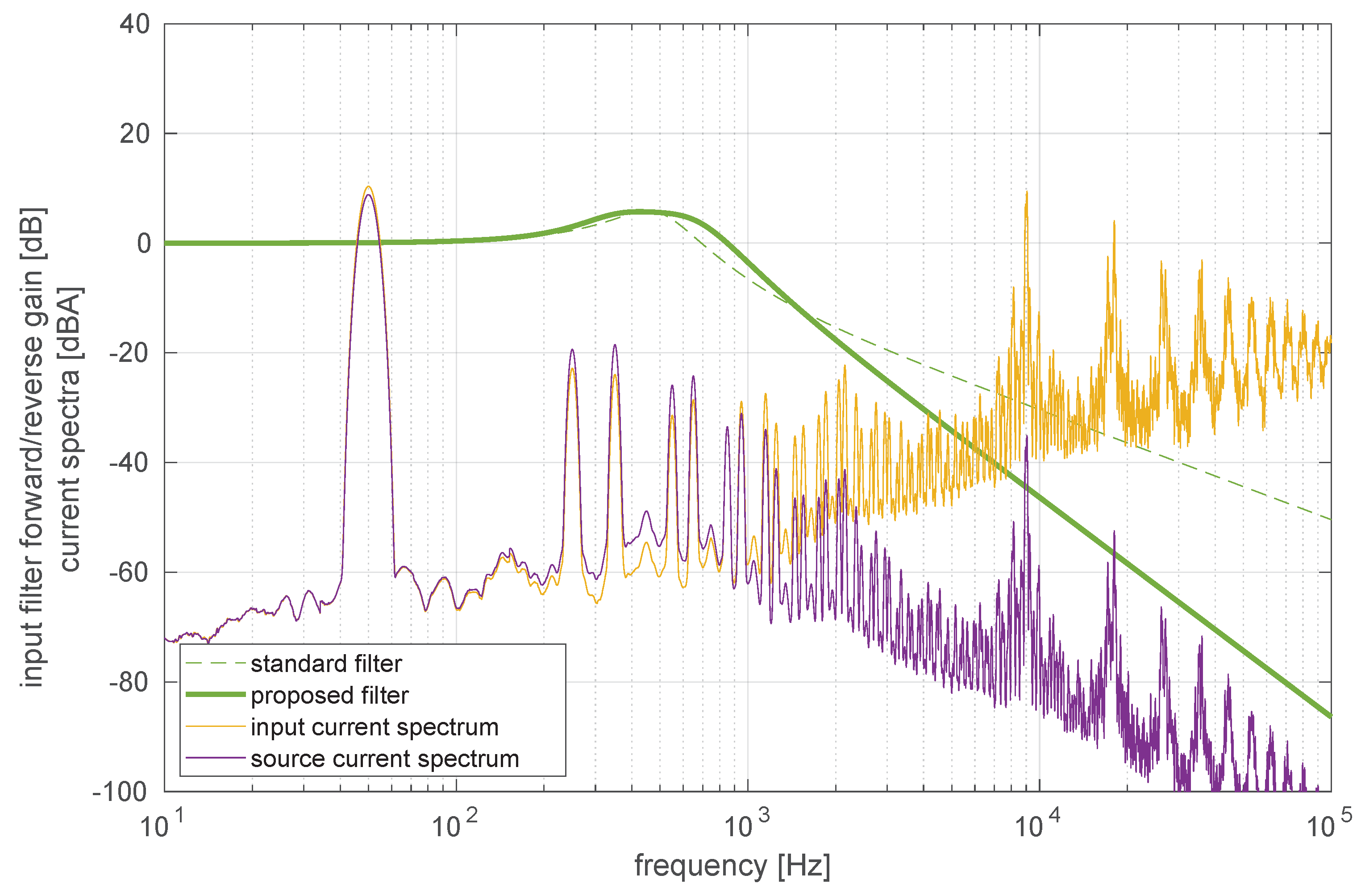
Let us focus on the input filter first. The first term of (36) is the effect of the interaction of the single-frequency line voltage on the filter input conductance . It means that to minimize losses, at line frequency should be as small as possible, but its behavior at other frequencies does not influence losses. The effect of the interaction of the matrix input current with the filter output resistance is instead more complicated. Figure 5 can help explain the behavior.
In the top panel, the thin yellow line represents the spectrum of the matrix input current , while the thin dashed lines represent the filter output resistance for various values of R. Larger values of R actually correspond to lower values of the output resistance at both low and high frequencies. This is important because the sigma-delta modulator puts most of the quantization noise above . Of course, the larger Rs produce sharper resonances, which cannot be accepted. A better solution is needed.
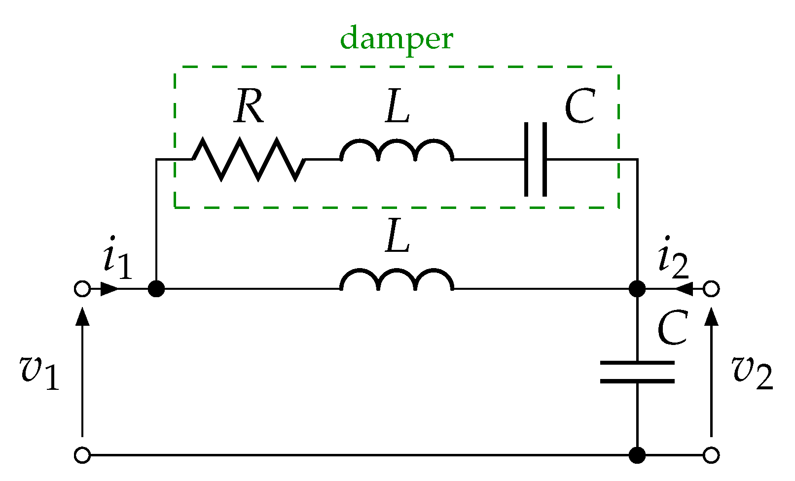
A simple modification can be done so that the losses act only at the resonance frequency, increasing the efficiency of the converter, using the circuit shown in Figure 6.
In it the series LC circuit connected to the resistor in the damper effectively enables the resistor only in proximity of the resonance frequency, where it is needed, and not elsewhere. The additional reactive components also have other positive effects on the filter transfer function that will be discussed in detail later. The main disadvantage of the filters is the higher cost, due to doubling the number of reactive components, but it must be noted that these additional components do not store a significant amount of power nor are subject to high voltages or currents, as can be seen from the specifications (obtained by simulation) reported in Table 1, so they can be much smaller and cheaper than the main ones, though must be of the same value.
The inverse hybrid representation of the filter in Figure 6 is equal to
which can also be seen in Figure 5, in solid lines. As can be seen, the behavior outside the resonance region is greatly improved, enabling the choice of a resistance to simultaneously dampen the resonance and achieve small losses. The bottom panel of the same figure shows the filters transfer functions (or , it’s the same) together with the resulting source current spectrum. Again, the proposed filter manifest a better behavior.
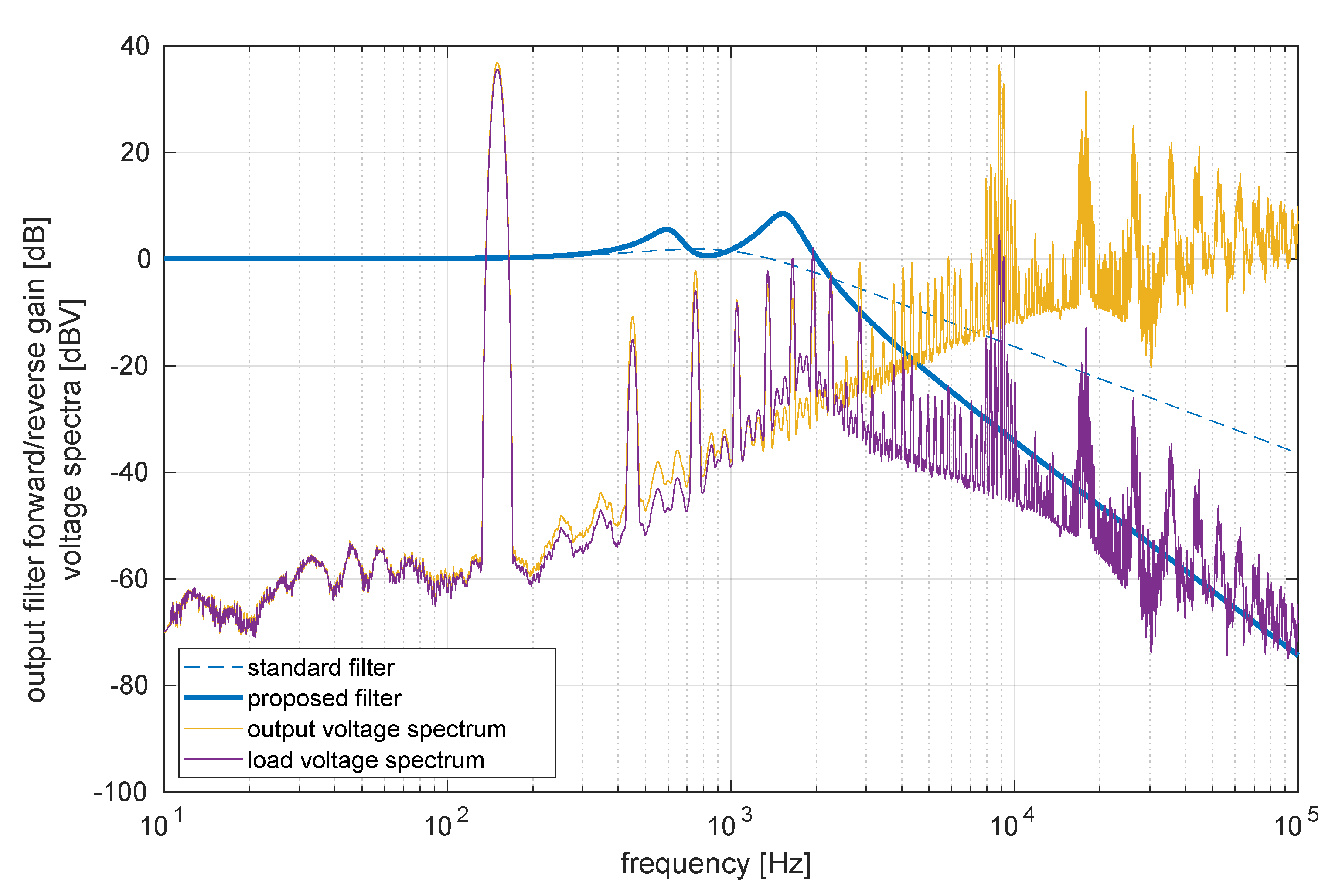
Similar considerations can be done for the output filter. Figure 7 shows its behavior.
This time the filter purpose is to filter the switched voltage present at the output of the matrix, and hence we are interested in its input conductance since in (36) it multiplies , while the output resistance multiplies the load current which is nearly sinusoidal. The improvement of the proposed filter in high-frequency behavior is even more apparent. Unfortunately, with the new filter architecture, the input conductance increases for increasing values of R, the opposite behavior than the traditional filter, and so a low resistor value had to be chosen to limit losses. Although it causes some peak splitting near resonance, the overall behavior is still satisfactory. Due to the higher frequency of the output voltage, a higher resonant frequency was also needed. The full specifications are reported in Table 2.
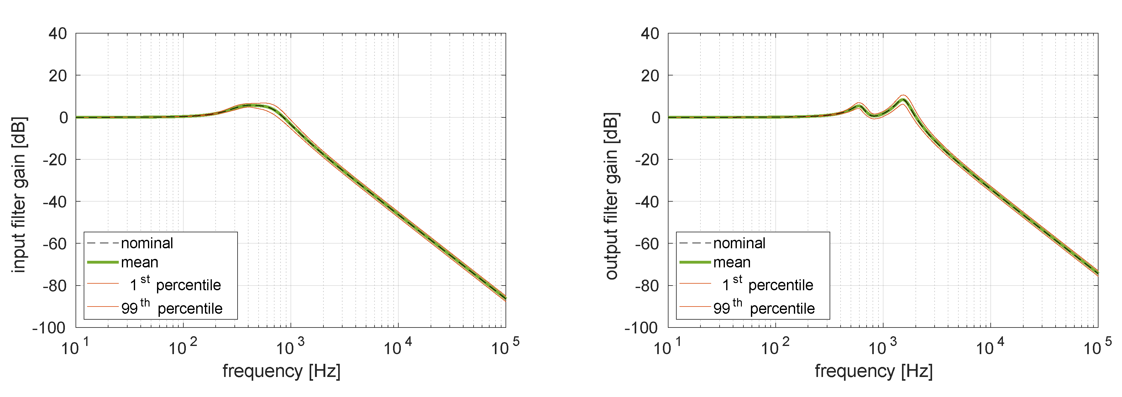
As previously stated, these filters need components that share the same value, though not the same rating, between the main, energy-passing filter, and the secondary, damper path. Actually, since the damping resistor causes a significant reduction of the resonance peak, as it is intended to do, it turns out that it is not strictly necessary to have an exact match of the component values between the main filter and the damper. Usual component tolerances can be accommodated for without affecting the intended behavior of the filter. This was confirmed by a Monte Carlo simulation, performed using 10% tolerance components. The results are reported in Figure 8. It shows the frequency responses of the two filters for the nominal case (thin dashed line), and the mean of 1000 Monte Carlo runs (thick solid line). The two are perfectly superimposed. The 1st and 99th percentiles are also shown (thin red lines) to highlight the expected range of variability of the frequency response: in 98% of the cases, the actual frequency response will lie within these lines. As can be seen, this variability is indeed quite small, and, most importantly, no artifacts ensue near resonance.
3. Simulation Results
The whole system was simulated using MATLAB SimScape using the component values reported in the tables above. To test it, we used a resistive-inductive load with and , driven at and , which results in an ideal output power of .
For comparison, the same system was also simulated with the sigma-delta modulator replaced by a conventional SVM controller. As a reference implementation, we chose the structure described in [22] with the input current displacement angle fixed at
where P is the active power and can be estimated at the load side, neglecting the effect of the output filter capacitor, by posing (load resistance), and (sum of load inductance and output filter inductance). Similarly, is estimated from the input side by neglecting the effects of the input filter inductor and using (input filter capacitance). To achieve comparable results, SVM employed the same modulation frequency, but the digital pulse-width modulation was performed using a 55× clock, i.e., , which is much higher than the sigma-delta clock. This was necessary as otherwise SVM would not have had enough modulation resolution to obtain the desired results, but it must be noted that a practical application of this SVM might require switching devices able to produce pulses, while the proposed sigma-delta modulator only uses pulses at worst.
Even from a computational complexity point of view, it must be stated that though SVM uses a much lower clock frequency to trigger computations (), these computations involve trigonometric functions [22], which are either time consuming or involve large look-up tables. On the other hand, the sigma-delta modulator needs a higher clock frequency (), but it only needs to advance four scalar second-order infinite impulse response (IIR) filters and perform some linear algebra computations per clock cycle. And all the matrices have only zeros or ones as coefficients so no multiplications are actually involved in most calculations.
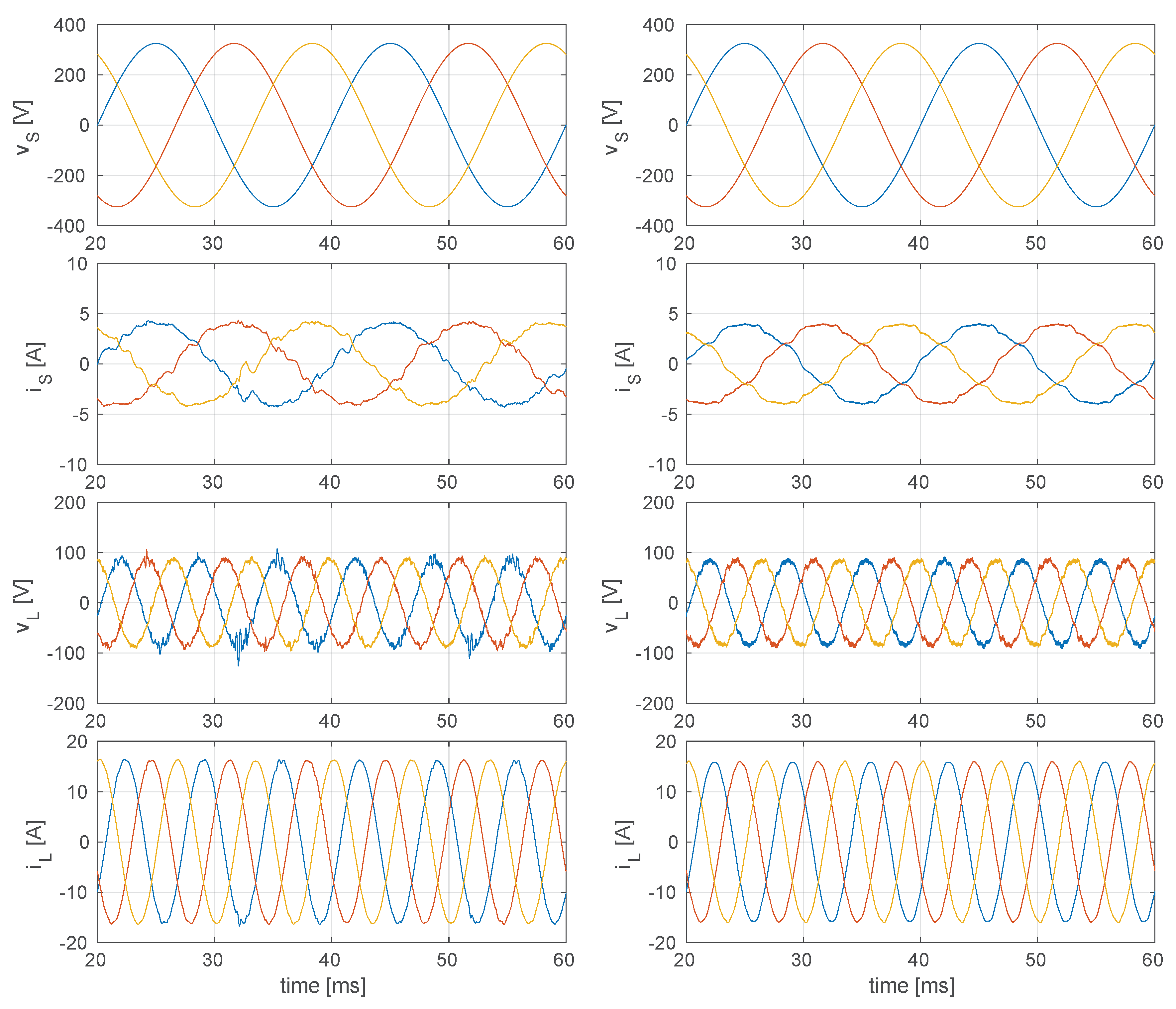
Figure 9 shows the load and source voltages and currents, the left panel is for the sigma-delta modulator, the right panel for the SVM algorithm. It is immediately apparent that the shape of the load current generated by the sigma-delta modulator is quite good, though some low frequency harmonics are still present in the source current. Their frequency content has already been reported in the bottom panels of Figure 5, for the source current, and Figure 7, for the load voltage, from which the harmonic content can be evaluated, as reported in Table 3. The SVM-produced waveforms have some residual high-frequency harmonics even after the strong filtering employed in this systems, as can be seen in their spectra reported in Figure 10.
Indeed, it is apparent from both Figure 10 and Table 3 that the proposed sigma-delta modulation is able to achieve a much lower harmonic distortion, as could be expected because the principle of operation of such modulator is to spread quantization noise over a large bandwidth, whose shape is determined by the noise-shaping filter. Of course, if the noise is also added to the harmonic distortion (THD + N column of the table), the results become much more similar to SVM. It should nevertheless be noted that in many applications a wide-bandwidth noise can be more tolerated by the load, as a high harmonic content might cause, e.g., a motor to vibrate and produce audible tones.
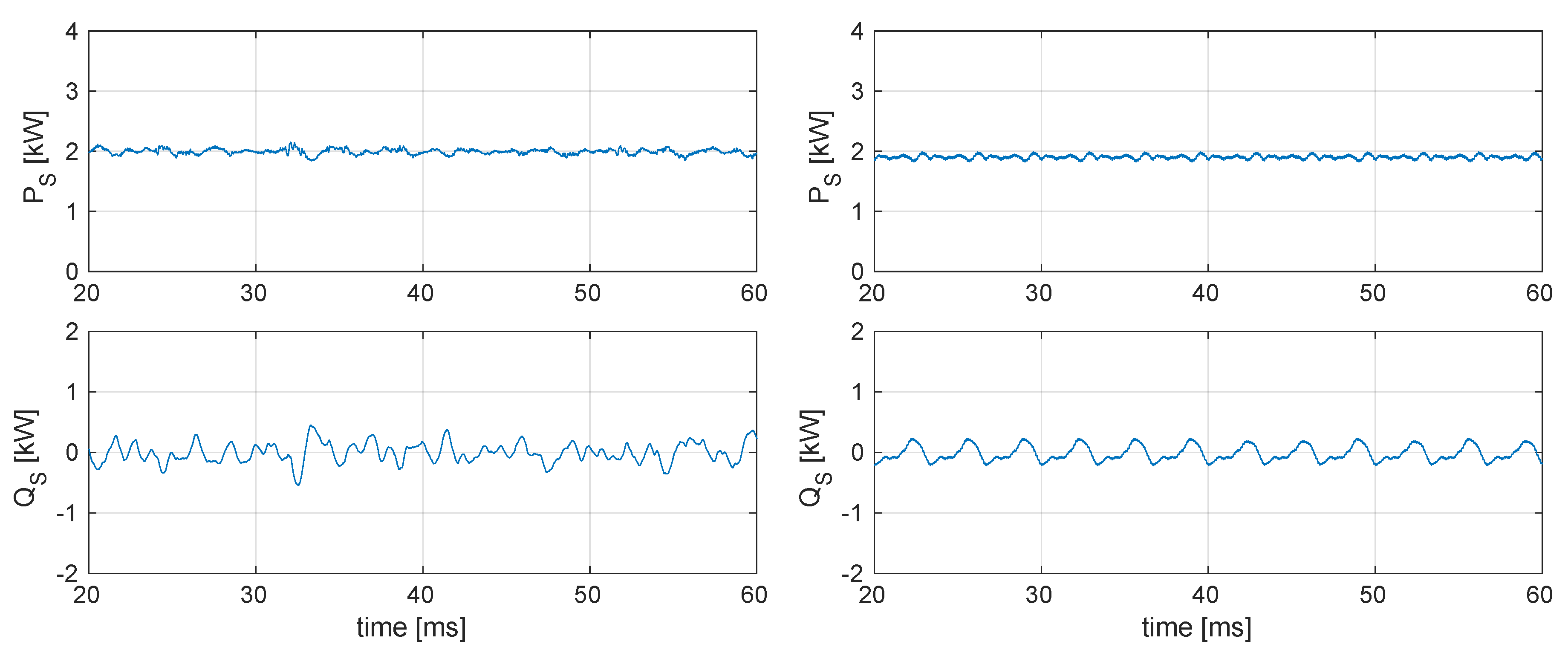
For what concerns instead the reactive power compensation, from the above figures it could already be seen that the source current is in phase with the source voltage, as required by the nulling of the input reactive power. This is also confirmed by Figure 11, that shows source active and reactive power, the latter being almost null on average. Again, the non-periodic nature of the artifacts produced by sigma-delta modulation is apparent compared to the periodic distortion of SVM.
The instantaneous three-phase power factor can finally be calculated as
where is the three-phase instantaneous active power and is the three-phase instantaneous reactive power at the source. It resulted on average equal to 0.997, a very good result.
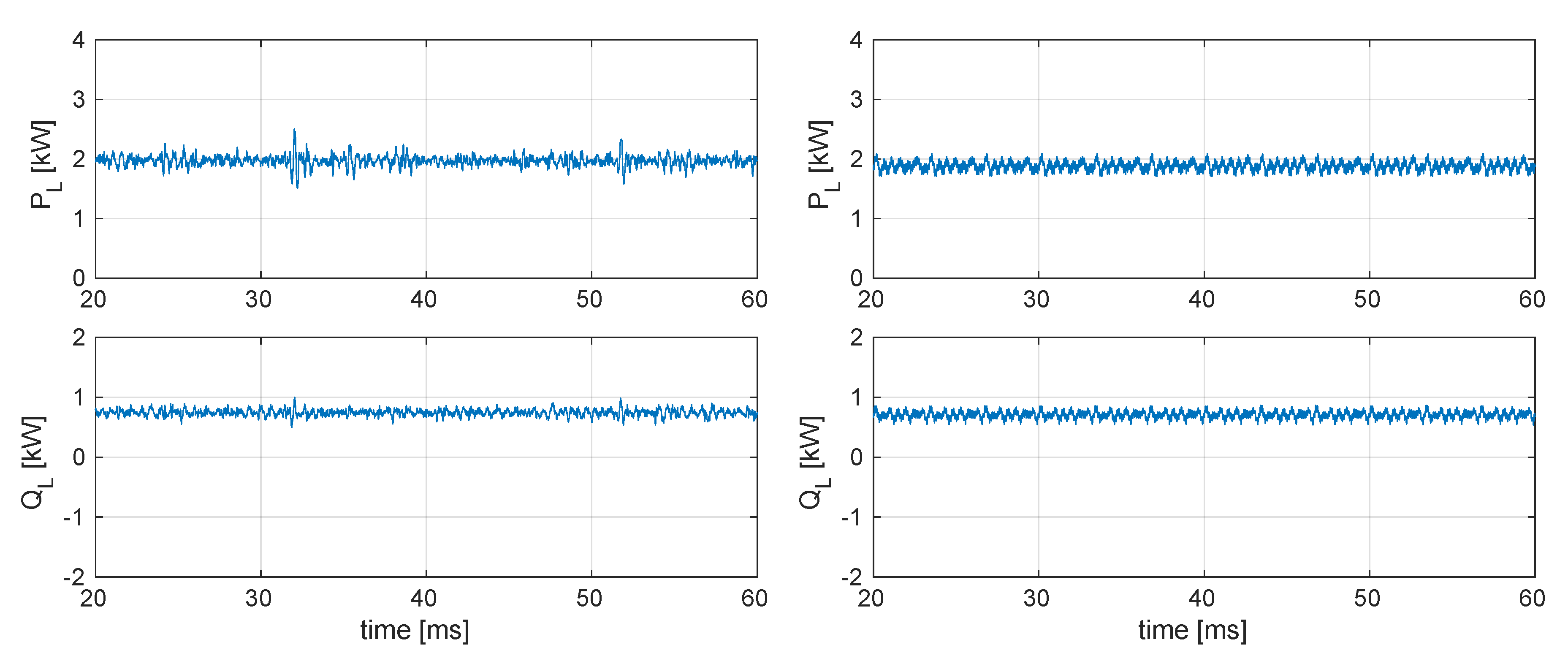
Similar results are reported in Figure 12 for the load.
The average powers obtained by simulation are summarized in Table 4, from where it is apparent that this converter can achieve a very high theoretical efficiency, since the filter losses amount to just over 1%, and that the load reactive power is nearly completely compensated by the converter.
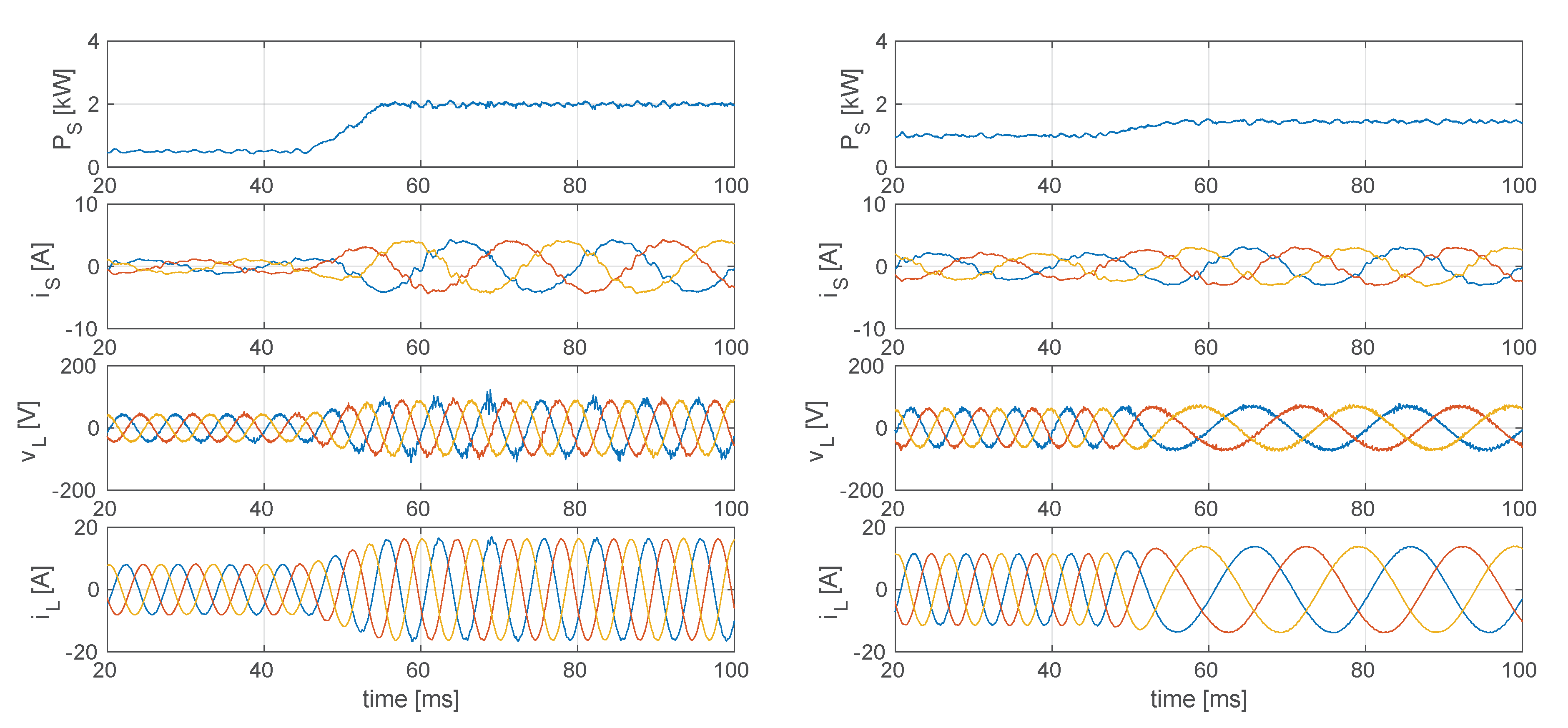
Finally, to test the performance of the proposed system under non-stationary conditions, a couple more simulations were performed imposing a change in desired voltage amplitude and frequency. Results are shown in Figure 13. On the left, output voltage was quickly increased from to during a interval, provoking a fourfold increase in output power. No significant artifacts can be seen in either the outputs or input current. On the right, the desired output frequency was lowered from to , causing a decrease in output reactive power, which is then accompanied by an increase in output active power having held constant the load voltage. It can easily be seen that this transition did not cause any change in the input current phase, showing that the reactive power compensation algorithm works as expected.
4. Conclusions
This work presents a new type of controlling algorithm for AC-AC matrix converters, based on modulation. It allows to compensate both source and load variations, as well as differences between an actual implementation and the ideal model, because the modulator measures critical electrical quantities and integrates and corrects for the past quantization errors occurred on the desired performance. It also allows to obtain arbitrary output waveforms with a null homopolar component.
Simulation results show that excellent performance can be obtained in terms of control accuracy and quality of load and source currents. Crucial in the achievement of these performances are the proposed line filters, suitable for the noise spectrum produced by the controller.
Author Contributions
Conceptualization, S.O., G.B. and P.C.; Formal analysis, S.O. and G.B.; Investigation, S.O.; Methodology, S.O.; Software, S.O. and G.B.; Validation, S.O. and G.B.; Writing—original draft, S.O., G.B. and P.C.; Writing—review & editing, S.O., G.B. and L.F.
Funding
This research received no external funding. The APC was funded by authors’ institution.
Conflicts of Interest
The authors declare no conflict of interest. The funders had no role in the design of the study; in the collection, analyses, or interpretation of data; in the writing of the manuscript, or in the decision to publish the results.
References
- Rodriguez, J.; Rivera, M.; Kolar, J.W.; Wheeler, P.W. A Review of Control and Modulation Methods for Matrix Converters. IEEE Trans. Ind. Electron. 2012, 59, 58–70. [Google Scholar] [CrossRef]
- Mohamad, A.S. Modeling of a steady-state VSCF aircraft electrical generator based on a matrix converter with high number of input phases. In Proceedings of the 2015 IEEE Student Conference on Research and Development (SCOReD), Kuala Lumpur, Malaysia, 13–14 December 2015; pp. 500–505. [Google Scholar]
- Aten, M.; Towers, G.; Whitley, C.; Wheeler, P.; Clare, J.; Bradley, K. Reliability comparison of matrix and other converter topologies. IEEE Trans. Aerosp. Electron. Syst. 2006, 42, 867–875. [Google Scholar] [CrossRef]
- Ali, S.; Wolfs, P. A matrix converter based voltage regulator for MV rural feeders. In Proceedings of the 2014 IEEE PES General Meeting Conference & Exposition, National Harbor, MD, USA, 27–31 July 2014; pp. 1–5. [Google Scholar]
- Abdel-Rahim, O.; Funato, H.; Abu-Rub, H.; Ellabban, O. Multiphase wind energy generation with direct matrix converter. In Proceedings of the 2014 IEEE International Conference on Industrial Technology (ICIT), Busan, Korea, 26 February–1 March 2014; pp. 519–523. [Google Scholar]
- Raja, K.M.; Vijayakumar, K.; Kannan, S. Matrix converter based solar photo voltaic system for reactive power compensation using sinusoidal pulse width modulation. In Proceedings of the 2014 IEEE International Conference on Computational Intelligence and Computing Research (ICCIC), Coimbatore, India, 18–20 December 2014; pp. 1–5. [Google Scholar]
- Bucknall, R.W.G.; Ciaramella, K.M. On the conceptual design and performance of a matrix converter for marine electric propulsion. IEEE Trans. Power Electron. 2010, 25, 1497–1508. [Google Scholar] [CrossRef]
- Li, G.; Yu, S.; Jia, S.; Wang, Q. Control of three phases—Single phase matrix converter for transient electromagnetic sounding. In Proceedings of the 17th International Conference on Electrical Machines and Systems (ICEMS), Hangzhou, China, 22–25 October 2014; pp. 3074–3077. [Google Scholar]
- Sandoval, J.J.; Essakiappan, S.; Enjeti, P. A bidirectional series resonant matrix converter topology for electric vehicle dc fast charging. In Proceedings of the 2015 IEEE Applied Power Electronics Conference and Exposition (APEC), Charlotte, NC, USA, 15–19 March 2015; pp. 3109–3116. [Google Scholar]
- Venugopal, L.V.; Jayapal, R. Matrix converter based energy saving for street lights. In Proceedings of the 2015 International Conference on Circuit, Power and Computing Technologies (ICCPCT), Nagercoil, India, 19–20 March 2015; pp. 1–6. [Google Scholar]
- Venturini, M.; Alesina, A. The generalised transformer: A new bidirectional, sinusoidal waveform frequency converter with continuously adjustable input power factor. In Proceedings of the 1980 IEEE Power Electronics Specialists Conference, Atlanta, GA, USA, 16–20 June 1980; pp. 242–252. [Google Scholar] [CrossRef]
- Alesina, A.; Venturini, M. Analysis and design of optimum-amplitude nine-switch direct AC-AC converters. IEEE Trans. Power Electron. 1989, 4, 101–112. [Google Scholar] [CrossRef]
- Ziogas, P.D.; Kang, Y.G.; Stefanovic, V.R. Rectifier-Inverter Frequency Changers with Suppressed DC Link Components. IEEE Trans. Ind. Appl. 1986, 22, 1027–1036. [Google Scholar] [CrossRef]
- Casadei, D.; Serra, G.; Tani, A.; Zarri, L. Optimal Use of Zero Vectors for Minimizing the Output Current Distortion in Matrix Converters. IEEE Trans. Ind. Electron. 2009, 56, 326–336. [Google Scholar] [CrossRef]
- Huber, L.; Borojevic, D. Space vector modulator for forced commutated cycloconverters. In Proceedings of the Conference Record of the IEEE Industry Applications Society Annual Meeting, San Diego, CA, USA, 1–5 October 1989; Volume 1, pp. 871–876. [Google Scholar] [CrossRef]
- Huber, L.; Borojevic, D. Space vector modulated three-phase to three-phase matrix converter with input power factor correction. IEEE Trans. Ind. Appl. 1995, 31, 1234–1246. [Google Scholar] [CrossRef]
- Aziz, P.M.; Sorensen, H.V.; Van der Spiegel, J. An Overview of Sigma-Delta Converters. IEEE Signal Process. Mag. 1996, 13, 61–84. [Google Scholar] [CrossRef]
- Orcioni, S.; d’Aparo, R.D.; Conti, M. A Switching Mode Power Supply with Digital Pulse Density Modulation Control. In Proceedings of the 18th European Conference on IEEE European Conference on Circuit Theory and Design (ECCTD-2007), Seville, Spain, 27–30 August 2007; pp. 603–606. [Google Scholar] [CrossRef]
- Orcioni, S.; d’Aparo, R.; Lobascio, A.; Conti, M. Dynamic OSR dithered sigma–delta modulation in solid state light dimming. Int. J. Circuit Theory Appl. 2013, 41, 387–395. [Google Scholar] [CrossRef]
- Orcioni, S.; Biagetti, G.; Crippa, P.; Falaschetti, L.; Turchetti, C. Sigma-Delta Based Modulation Method for Matrix Converters. In Proceedings of the 2018 IEEE International Conference on Environment and Electrical Engineering and 2018 IEEE Industrial and Commercial Power Systems Europe (EEEIC/I&CPS Europe), Palermo, Italy, 12–15 June 2018; pp. 1–5. [Google Scholar]
- Akagi, H.; Kanazawa, Y.; Nabae, A. Instantaneous reactive power compensators comprising switching devices without energy storage components. IEEE Trans. Ind. Appl. 1984, 20, 625–630. [Google Scholar] [CrossRef]
- Nguyen, H.M.; Lee, H.; Chun, T. Input Power Factor Compensation Algorithms Using a New Direct-SVM Method for Matrix Converter. IEEE Trans. Ind. Electron. 2011, 58, 232–243. [Google Scholar] [CrossRef]
Figure 1.
Analog part of the converter, comprising the direct matrix, the input and output filters, and the voltage and current analog-to-digital (AD) converters.
Figure 1.
Analog part of the converter, comprising the direct matrix, the input and output filters, and the voltage and current analog-to-digital (AD) converters.

Figure 2.
The Sigma-Delta digital modulator, acting as controller of the matrix converter.

Figure 3.
Example of the switching sequence obtained by the sigma-delta modulator.

Figure 4.
Standard line/load filter with purely resistive damper.

Figure 5.
Input filter behavior: output resistance and gain on the top and bottom panel, respectively. Input and source current spectrum on the top and bottom panel, respectively.
Figure 5.
Input filter behavior: output resistance and gain on the top and bottom panel, respectively. Input and source current spectrum on the top and bottom panel, respectively.

Figure 6.
Proposed line/load filter with resonant resistive damper.

Figure 7.
Output filter behavior: input conductance and gain on the top and bottom panel, respectively. Output and load voltage spectrum on the top and bottom panel, respectively.
Figure 7.
Output filter behavior: input conductance and gain on the top and bottom panel, respectively. Output and load voltage spectrum on the top and bottom panel, respectively.

Figure 8.
Frequency response of the proposed line/load filter with resonant resistive damper, with variations due to a 10% tolerance in the passive components.
Figure 8.
Frequency response of the proposed line/load filter with resonant resistive damper, with variations due to a 10% tolerance in the passive components.

Figure 9.
Simulation results of the electrical quantities at the source (, ), and at the load (, ). (Left panel) as obtained by the proposed sigma-delta modulator. (Right panel) as produced by a reference implementation of SVM.
Figure 9.
Simulation results of the electrical quantities at the source (, ), and at the load (, ). (Left panel) as obtained by the proposed sigma-delta modulator. (Right panel) as produced by a reference implementation of SVM.

Figure 10.
Spectra of the source current and load voltage obtained by SVM.


Figure 11.
Simulation results of the active and reactive power at the source (, ). (Left): sigma-delta modulator. (Right): SVM.
Figure 11.
Simulation results of the active and reactive power at the source (, ). (Left): sigma-delta modulator. (Right): SVM.

Figure 12.
Simulation results of the active and reactive power at the load (, ). (Left): sigma-delta modulator. (Right): SVM.
Figure 12.
Simulation results of the active and reactive power at the load (, ). (Left): sigma-delta modulator. (Right): SVM.

Figure 13.
Simulation results of the electrical quantities at the source (, ), and at the load (, ), during transients of desired output voltage. In the (left panel) the desired amplitude was ramped from to from time to time , so that the power ramps from about to about . In the (right panel) the desired frequency was swept from to during the same time span, while the voltage was held constant at . Power starts at about and then rises due to lower reactance of load.


Table 1.
Specifications of the input filter. The resulting cut-off frequency is .
| Component | Value | Rating [RMS] | Rating [max] |
|---|---|---|---|
| Main inductor | |||
| Main capacitor | |||
| Damper inductor | |||
| Damper capacitor | |||
| Damper resistor |
Table 2.
Specifications of the output filter. The resulting cut-off frequency is .
| Component | Value | Rating [RMS] | Rating [max] |
|---|---|---|---|
| Main inductor | |||
| Main capacitor | |||
| Damper inductor | |||
| Damper capacitor | |||
| Damper resistor |
Table 3.
Comparison of total harmonic distortion (THD) and total harmonic distortion plus noise (THD + N) for and SVM.
Table 3.
Comparison of total harmonic distortion (THD) and total harmonic distortion plus noise (THD + N) for and SVM.
| THD | THD + N | |||||
|---|---|---|---|---|---|---|
| Quantity | SVM | SVM | ||||
| 0.78% | 5.11% | 6.71% | 5.13% | |||
| 0.27% | 0.98% | 1.27% | 0.99% | |||
| 3.98% | 6.72% | 8.82% | 6.74% | |||
Table 4.
Summary of the average power consumption in the matrix converter. The overall efficiency is 98.7%.
Table 4.
Summary of the average power consumption in the matrix converter. The overall efficiency is 98.7%.
| Entity | Active Power [kW] | Reactive Power [kW] | Power Factor |
|---|---|---|---|
| Source | 0.997 | ||
| Load | — | ||
| Input filter | — | ||
| Output filter | — |
© 2019 by the authors. Licensee MDPI, Basel, Switzerland. This article is an open access article distributed under the terms and conditions of the Creative Commons Attribution (CC BY) license (http://creativecommons.org/licenses/by/4.0/).
Share and Cite
MDPI and ACS Style
Orcioni, S.; Biagetti, G.; Crippa, P.; Falaschetti, L. A Driving Technique for AC-AC Direct Matrix Converters Based on Sigma-Delta Modulation. Energies 2019, 12, 1103. https://doi.org/10.3390/en12061103
AMA Style
Orcioni S, Biagetti G, Crippa P, Falaschetti L. A Driving Technique for AC-AC Direct Matrix Converters Based on Sigma-Delta Modulation. Energies. 2019; 12(6):1103. https://doi.org/10.3390/en12061103
Chicago/Turabian StyleOrcioni, Simone, Giorgio Biagetti, Paolo Crippa, and Laura Falaschetti. 2019. "A Driving Technique for AC-AC Direct Matrix Converters Based on Sigma-Delta Modulation" Energies 12, no. 6: 1103. https://doi.org/10.3390/en12061103
Note that from the first issue of 2016, this journal uses article numbers instead of page numbers. See further details here.