Article

Voltage Jump Suppression and Capacitor Voltage Fluctuation Analysis for a Four-Level Hybrid Flying Capacitor T-Type Converter

1
School of Electrical and Power Engineering, China University of Mining and Technology, Xuzhou 221116, China
2
Department of Electrical and Electronic Engineering, University of Bristol, Bristol BS8 1TH, UK
*
Author to whom correspondence should be addressed.
Energies 2019, 12(4), 698; https://doi.org/10.3390/en12040698
Submission received: 21 January 2019 / Revised: 8 February 2019 / Accepted: 18 February 2019 / Published: 21 February 2019

Abstract

:
In low and medium voltage power conversion systems, multilevel converters are becoming more and more attractive due to improved power density. However, the complexity of topology and control is a big challenge for the application of multilevel converters. In this paper, a four-level (4L) hybrid flying capacitor (FC) T-type converter has been researched in detail. The topological advantage of the converter is displayed in comparison to existing four-level converters. According to the feature of the topology, the operating status has been analyzed and the reason for the voltage jump is researched in detail during the dead-time period. A strategy to reduce voltage jump by adjusting the switching states has be presented. The FC voltages can be balanced by selecting the appropriate switching states. The relationships between the fluctuations of FC voltages and the modulation index and power factor (PF) have been analyzed by simulation results. The performance of the 4L converter has been investigated in MATLAB/Simulink as well as on a down-scaled laboratory prototype.

Graphical Abstract

1. Introduction

Thanks to lower harmonic distortion, switching stress and electromagnetic interference (EMI), multilevel converters are widely used in medium-voltage high-power applications, such as motor drives, renewable power generations and microgrids, etc. [1,2,3]. Meanwhile, due to lower switching losses and reduced cooling and filter requirements, multilevel converters are also becoming more and more popular in low voltage application (e.g., 380 V) where high-density design is required, such as aerospace, electric vehicles and renewable energy [4,5].
The three classic converters are neutral-point-clamped (NPC) converters, flying capacitor (FC) converters and cascaded H-bridge (CHB) converters. They each have their own advantages and disadvantages. For NPC converters, the voltage stress across each switch is the same, so it can be suitable for medium/high voltage high power applications. However, with a higher number of voltage levels, it needs plenty of clamping diodes and the dc-link capacitor voltages are difficult to control. The FC converter does not have a dc-link neutral points balance issue as in the NPC converter, but the converter requires more flying capacitors when the voltage levels increase. Lots of capacitors may lead to increase the system volume and potentially degrade reliability. The CHB converter has a modular structure, and is easier to expand to higher voltage levels. However, a phase-shifted transformer is required to provide multiple separated power sources, which increases the system volume and cost [1,2,3,4].
Apart from the above three multilevel topologies, a variety of other multilevel converters have been proposed [6,7,8,9,10,11,12,13,14,15,16,17,18,19,20,21,22]. For instance, a 3L T-type converter was proposed which is suitable for low-voltage applications [6,7,8,9]. The T-type converter can have the same output voltage quality as the NPC converter, without the need for clamping diodes, but the two main switches need to block the full dc-link voltage. The active neutral-point clamped (ANPC) converter was proposed to solve an unbalanced loss distributions issue as in the NPC topologies [10,11,12,13,14,15,16]. The 3L ANPC has improved the 3L NPC by replacing the clamping diodes with clamping switches. By providing a controllable path for the neutral currents, this converter solves the uneven power loss distributions in the switching devices and improves the cooling system design [10,11,12,13]. However, the 3L ANPC converter need more switching devices than the 3L NPC. A 5L ANPC converter is a combination of a 3L ANPC converter and a 3L FC converter [14,15,16]. Its dc-link needs two capacitors and each leg has a flying capacitor and a total of 12 switching devices for a three-phase system. The converter can achieve higher voltage levels without adding series-connected diodes. However, the main drawback is the unequal voltage rating of the switching device. In each phase, the voltage ratings of the outer switches are half of the dc-link voltage and have twice the voltage ratings of the inner switches. References [17,18,19] have proposed a 4L hybrid-clamped (HC) converter. Although this converter has fewer passive components, it does add two more switches in each phase. A 4L nested neutral-point clamped (NNPC) converter was proposed in References [20,21,22] and is a combination of a 4L FC converter and a 3L NPC converter. In comparison with the classical four-level converters, the 4L NNPC converter has fewer clamping diodes and flying capacitors and all switches have the same voltage stress.
The 4L hybrid flying capacitor T-type converter was first derived in Figure 12 in Reference [5], and the basic principle of the converter was analyzed in Reference [23]. Then, the basic experimental validation of the converter was published in References [24,25]. However, the operating status of the converter, especially during the dead-time, has not been analyzed in detail. In this paper, this converter is researched in more detail. The advantages and disadvantages of the topology have been displayed in comparison to existing four-level converters. The operations of this converter are analyzed and the reason for the voltage jump has been illustrated in detail during the dead-time period. Then, a strategy for avoiding/reducing the voltage jump during the dead-time period by adjusting the switching states has been presented. The effect on the flying capacitor (FC) voltages under all switching states has been analyzed and the FC voltages can be balanced by selecting the appropriate switching states. Meanwhile, the relationship between the fluctuations of the FC voltages and the modulation index and PF is revealed in depth.
The rest of this paper is organized as follows: Section 2 shows the advantages and disadvantages of the topology and analyzes the operations; Section 3 analyzes the flying capacitor voltages control method; Section 4 shows simulation results to investigate the performance of the converter. FC voltage fluctuations are analyzed in detail; Section 5 shows the experimental results, which validates the topology and corresponding control strategy; Section 6 concludes the paper.

2. Analysis of the Converter Topology

2.1. Comparison of Four-Level Topologies

The 4L hybrid converter is shown in Figure 1. Table 1 shows a comparison of various 4L converters. From this table, the advantages and disadvantages of the converter can be summarized as follows:
Advantages: Compared with existing 4L converters, the 4L hybrid converter has no clamping diodes, fewer switches and FCs, and only one dc-link capacitor. Therefore, the topology is simpler and does not need to control the dc-link capacitor voltages, which reduces the control complexity.
Disadvantages: For the four-level converter, the voltage stress of each switch is unequal. The withstanding voltages of the switches Tx2 and Tx5 are 2Vdc/3 and twice the value of other switches. Therefore, the voltage rating requirements for Tx2 and Tx5 are higher than other switches and these high voltage devices can be expensive for high voltage applications.

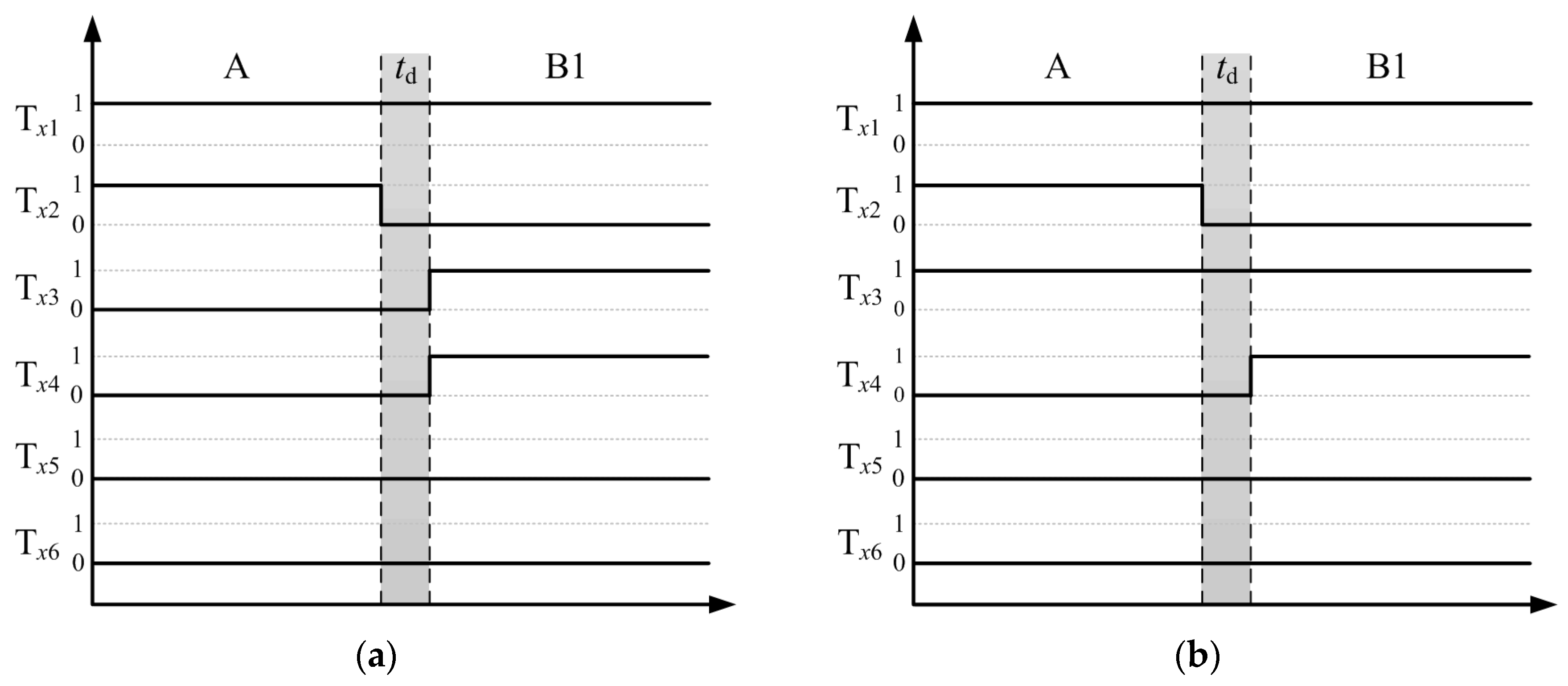
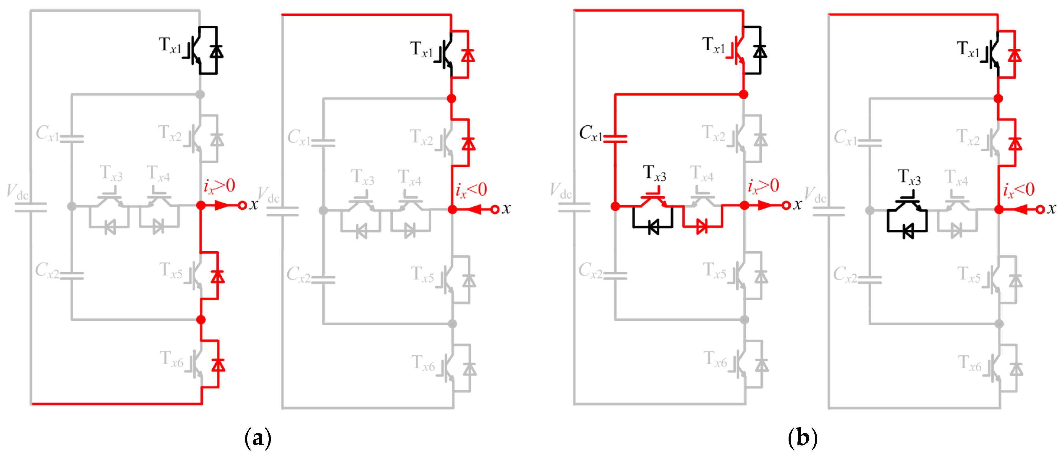
2.2. Operation of the Converter

In order to generate four output voltage steps, the converter needs to control the voltages of the flying capacitors Cx1 and Cx2 (x = a, b, c) to be Vdc/3. Hence, the four output voltages, Vxo, are Vdc, 2Vdc/3, Vdc/3, and 0, and the voltage levels are 3, 2, 1, and 0.
When the converter generates four output voltage levels, there are six phase current paths as shown in Figure 2, where the corresponding switches need to be turned on. Hence, all the six basic switching states according to six current paths in each phase leg are given in Table 2.
When the converter commutes between the switching states, it is necessary to avoid the short-circuit of capacitors. Therefore, a dead-time is added at the rising edge of the gating pulses to avoid a short-circuit. In order to investigate the operations of the converter during the dead-time, the switching states from A to B1 are analyzed in one phase leg as an example. When the basic switching states commute from A to B1, the switching patterns are shown in Figure 3a, while the current paths are shown in Figure 4a during the dead-time period. From Figure 3a, during the dead-time, only switch Tx1 is turned on and the other switches are OFF. Therefore, the freewheeling diodes of Tx5 and Tx6 are conducting when ix > 0, and the output voltage is 0, as shown in Figure 4a. When ix < 0, the freewheeling diodes of Tx1 and Tx2 are conducting, and the output voltage is Vdc at this time. In this case, the converter output voltage is jumping three levels from Vdc to 0 when ix > 0. It will cause higher switching voltage stress (higher dv/dt). In order to eliminate this voltage jump, the basic switching states are adjusted as shown in Table 3, where the states of switches Tx1 and Tx6, Tx2 and Tx4, and Tx3 and Tx5 are complementary. For example, if the state of Tx1 is ON, the state of Tx6 must be OFF. After adjustments, for the same transition from A to B1, the switching patterns are shown in Figure 3b, and the current paths are shown in Figure 4b. During the dead-time, the switches Tx1 and Tx3 are ON, and other switches are OFF. The freewheeling diode of Tx4 and the switches Tx1 and Tx3 are conducting when ix > 0, and the output voltage is 2Vdc/3. When ix < 0, the freewheeling diodes of Tx1 and Tx2 are conducting, and the output voltage is Vdc at this time. The converter output voltage is only jumping one level from Vdc to 2Vdc/3 when ix > 0. Therefore, the switching voltage stress can be effectively reduced after adjusting the switching states. Similar adjustments can be made for transitions between other switching states as shown in Table 3 during the dead-time.
However, in one case, it is inevitable that the output voltage of the converter will jump two levels. When the adjusted switching states commute from B2 to C1, no switch is ON during the dead-time. At this instant, the freewheeling diodes of Tx5 and Tx6 are conducting and the output voltage is 0 when ix is positive. The freewheeling diodes of Tx1 and Tx2 are conducting and the output voltage is Vdc when ix is negative. The converter output voltage will jump two levels from 2Vdc/3 to 0 when ix > 0. Therefore, this voltage jump is inevitable. However, the adjusted switching states shown in Table 3 can still reduce the switching voltage stress in all other cases.

3. Flying Capacitor Voltage Control Method

3.1. Analysis of the Flying Capacitor Voltages

In order to control the FC voltages at Vdc/3, the condition of the FCs must be analyzed under all switching states. The voltages of Cx1 and Cx2 are denoted by VCx1 and VCx2.
From Figure 2a,f, it can be seen that there are no currents flowing through the FCs when output levels are 3 and 0. Thus, the FC voltages do not change. When output levels are 2 and 1, there are two redundant switching states respectively as shown in Table 3. Different switching states have different effects on the FC voltages. For the switching state B1, the current only flows through the Cx1 as shown in Figure 2b. When ix > 0, the Cx1 is charged, and when ix < 0, the Cx1 is discharged, while there is no effect on the Cx2. For the switching state B2, the current flows through both FCs as shown in Figure 2c. When ix > 0, the Cx1 and Cx2 are discharged, and when ix < 0, the Cx1 and Cx2 are charged. For output level 1, the effects on the FC voltages can also be analyzed in a similar way. The conditions of the FC voltages are summarized in Table 4. Based on the conditions of the FC voltages under all switching states, the FC voltages can be controlled at the desired value Vdc/3 by selecting the appropriate switching states.

3.2. Control of the Flying Capacitor Voltages

The deviations which are defined as the difference between the actual FC voltages and the desired value can be expressed as:
Δ V C x k = V C x k V C x k . ref
where VCxk are the actual FC voltages, VCxk.ref are the desired values which are Vdc/3, and ΔVCxk are the deviations of the FC voltages, x = a, b, c and k = 1, 2.
In order to control the FC voltages to be Vdc/3, the deviations of the FC voltages ΔVCxk should be controlled to be close to zero. If ΔVCxk > 0, the FCs should be discharged, whereas if ΔVCxk < 0, the FCs should be charged. According to the effects on the FC voltages under different switching states and directions of load currents as shown in Table 4, the FC voltages can be controlled at the desired value by selecting the appropriate switching states. Hence, the determination is shown in Figure 5.

4. Simulation Results

In order to investigate the performance of the 4L converter, a three-phase inverter has been simulated in MATLAB/Simulink (MATLAB 2017b, The MathWorks, Natick, MA, USA). The simulation parameters are shown in Table 5. The converter is modulated by using level shifted PWM in carrier-based PWM (CBPWM), which is the same as the phase disposition modulation as shown in Figure 2a in Reference [26]. The modulation index m is defined as:
m = 2 V ref V dc
where Vref is the amplitude of the phase voltage reference. The performance of the converter has been simulated.

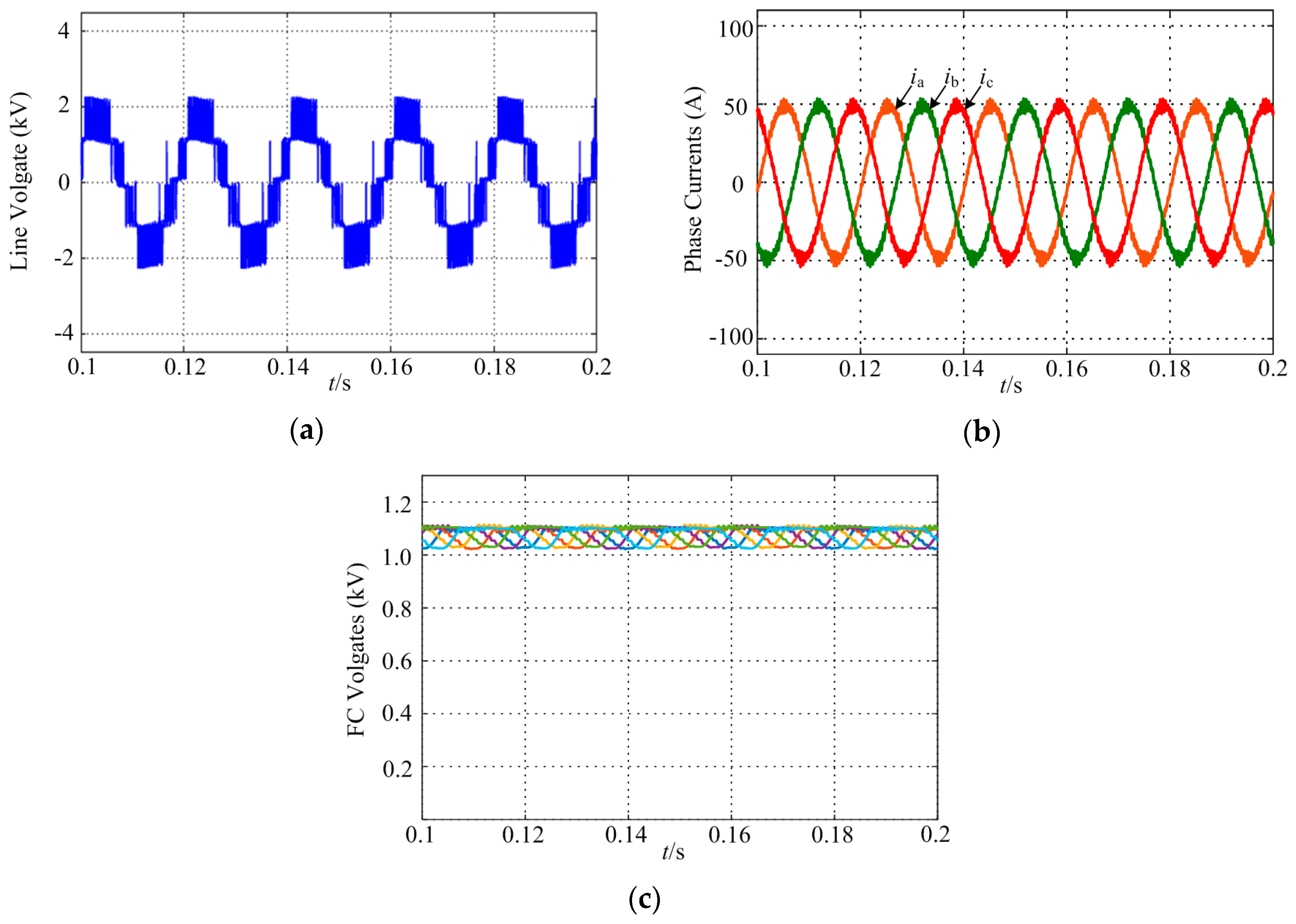
4.1. Steady State Simulation Recults

Figure 6 and Figure 7 show the steady state simulation results. Figure 6a shows the line voltage with m = 0.9 when the basic switching states in Table 2 are used, and Figure 6b shows the line voltage when the adjusted switching states in Table 3 are used. As shown in Figure 6a, the waveform of line voltage is seven voltage levels as expected, but there are large voltage jumps clearly in line voltage when the basic switching states are used. At this moment, the converter has higher switching voltage stress (dv/dt). In addition, the THD of line voltage is 30.37% as shown in Figure 6c. However, when the adjusted switching states are used, the voltage jumps are significantly decreased as shown in Figure 6b. Only some small voltage jumps remain which is inevitable as analyzed previously. The THD is reduced to 25.01% as shown in Figure 6d. The harmonics in the red area are significantly decreased. Therefore, the adjusted switching states can availably decrease the voltage jumps, and the switching voltage stress dv/dt can be effectively reduced, which is favored from the load perspective. The performance of the line voltage has been improved. Then, Figure 6e,f are the three phase currents waveforms and the FC voltages when m = 0.9. The three phase currents are highly sinusoidal, and FC voltages can be regulated at Vdc/3 = 1100 V. Figure 7 shows the line voltage, the three phase currents and the FC voltages when m = 0.6. From this figure, the waveform of line voltage is five voltage levels; the phase currents and FC voltages are also expected.

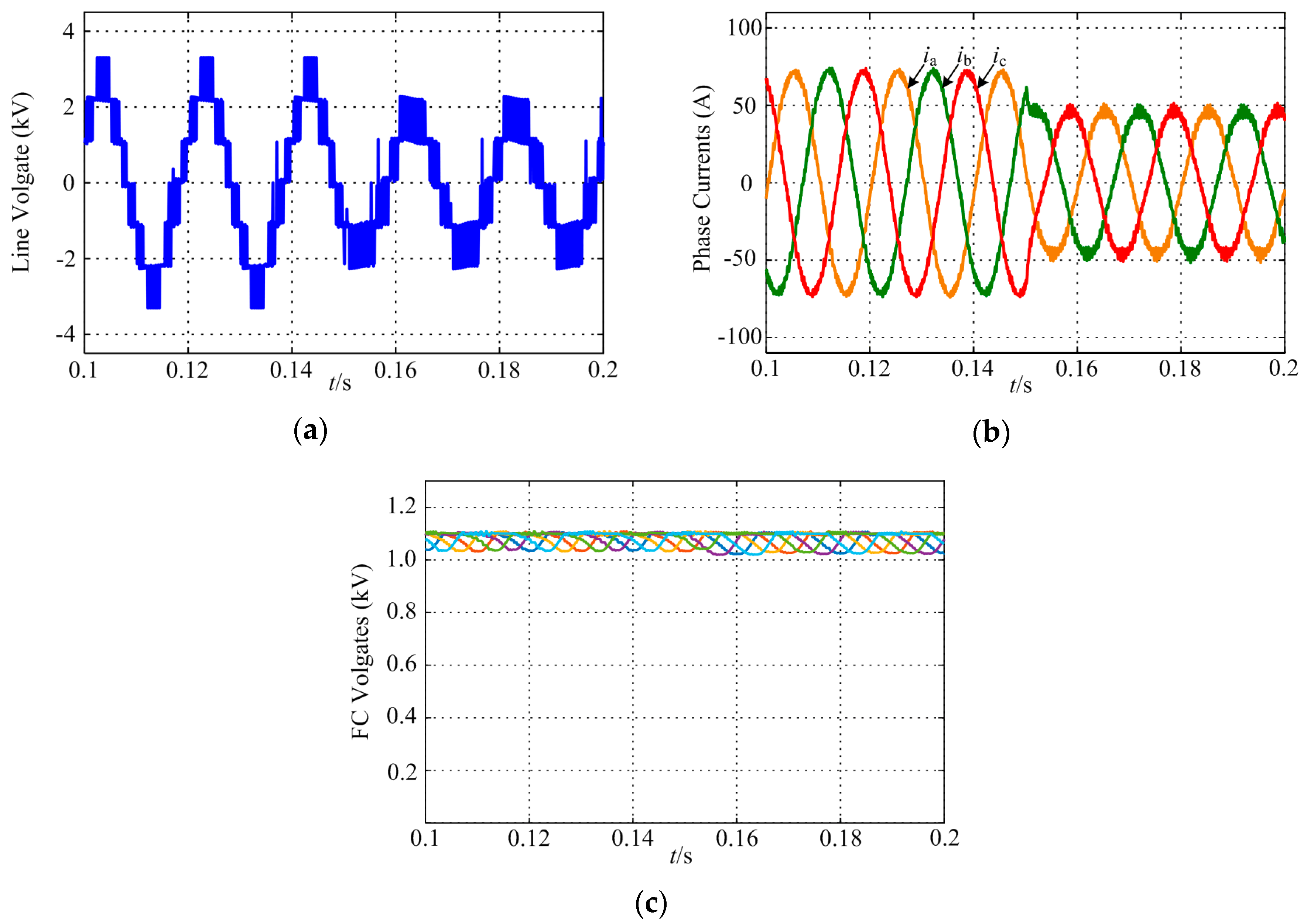
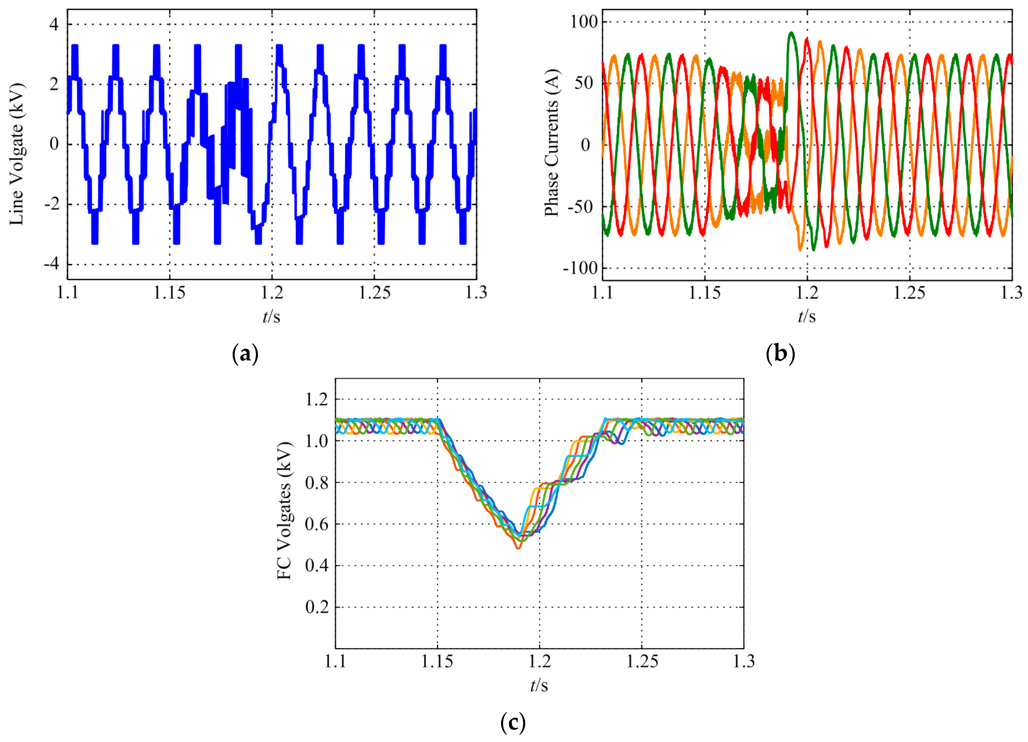
4.2. Transient State Simulation Results

Figure 8 and Figure 9 show the converter transient performance. Figure 8 shows the line voltage, the three phase currents and the FC voltages when m dynamically changes. As shown in Figure 8, the waveforms of line voltage are as expected, the three phase currents are also highly sinusoidal, and the FC voltages can always be regulated at the desired value of Vdc/3 = 1100 V, when m is changed from 0.9 to 0.6 at 0.15 s. Figure 9 shows the line voltage, the three phase currents and the FC voltages when the capacitor voltage control method is deactivated. When the capacitor voltage control method is deactivated at 1.15 s, all the FC voltages deviate from Vdc/3, and the line voltage and three phase currents are all distorted. When the capacitor voltage control method is reactivated at 1.19 s, the FC voltages can be again controlled at Vdc/3 = 1100 V, and the line voltage and the three phase currents return to normal.
Figure 10 shows the performance comparison of the 4L hybrid converter and 4L NNPC under different m and PF. The THDs of the two converters’ currents are almost the same as they both output voltages with four levels.
From simulation results under the steady and transient state, the converter can work properly. The FC voltages can be effectively controlled at Vdc/3 by using the capacitor voltage control method. Meanwhile, the phenomena of the undesired voltage jumps can be significantly decreased by using the adjusted switching states, which can effectively reduce the switching voltage stress (dv/dt). The performance of the 4L hybrid converter is almost the same as the 4L NNPC. The simulation results proved that the topology is feasible and voltage jump can be effectively reduced, and the performance of the line voltage has been improved.

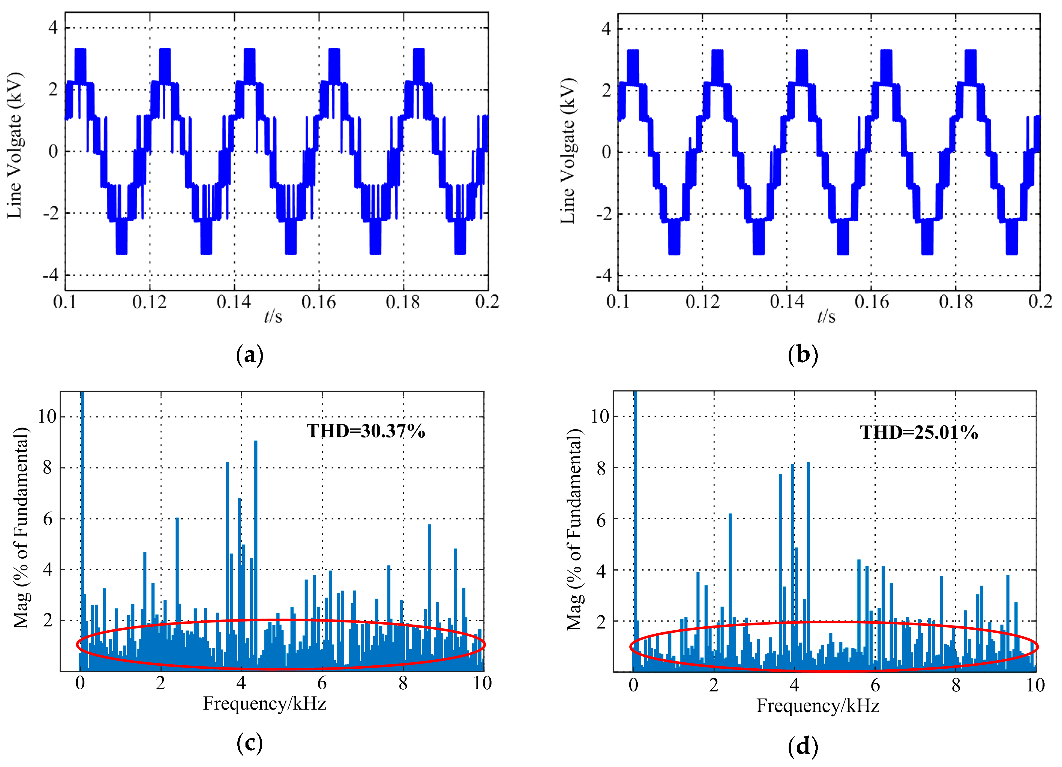
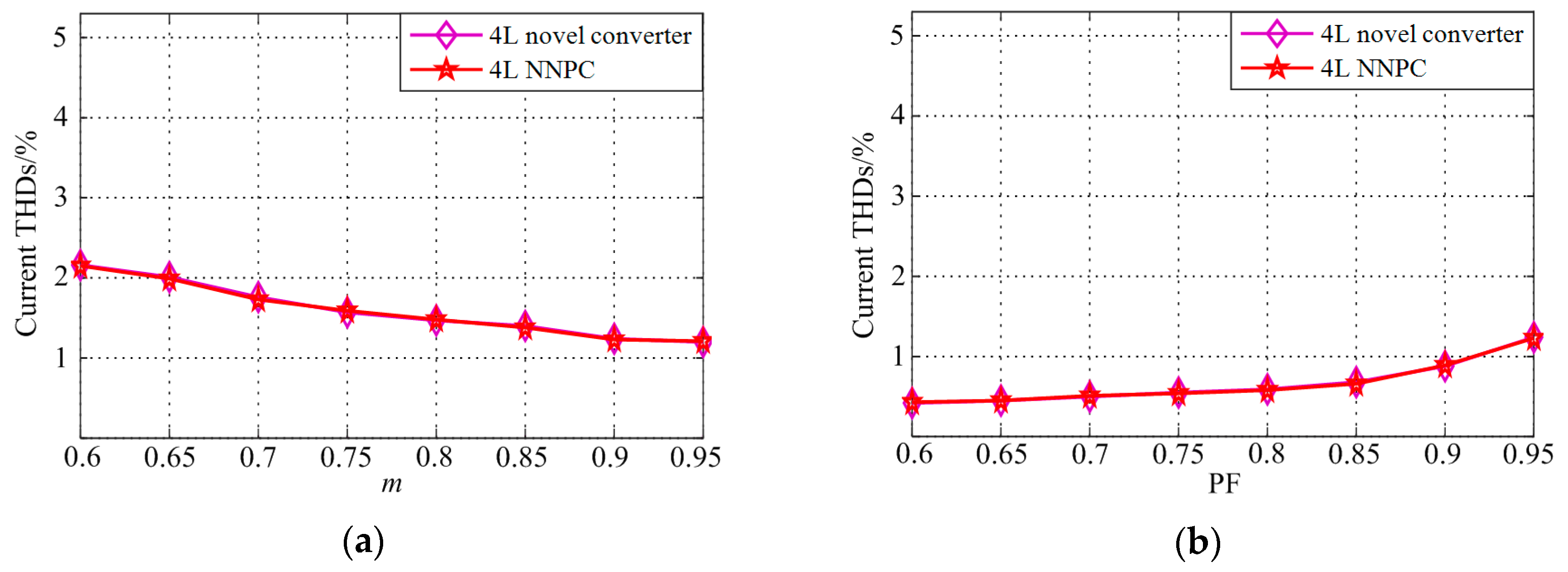
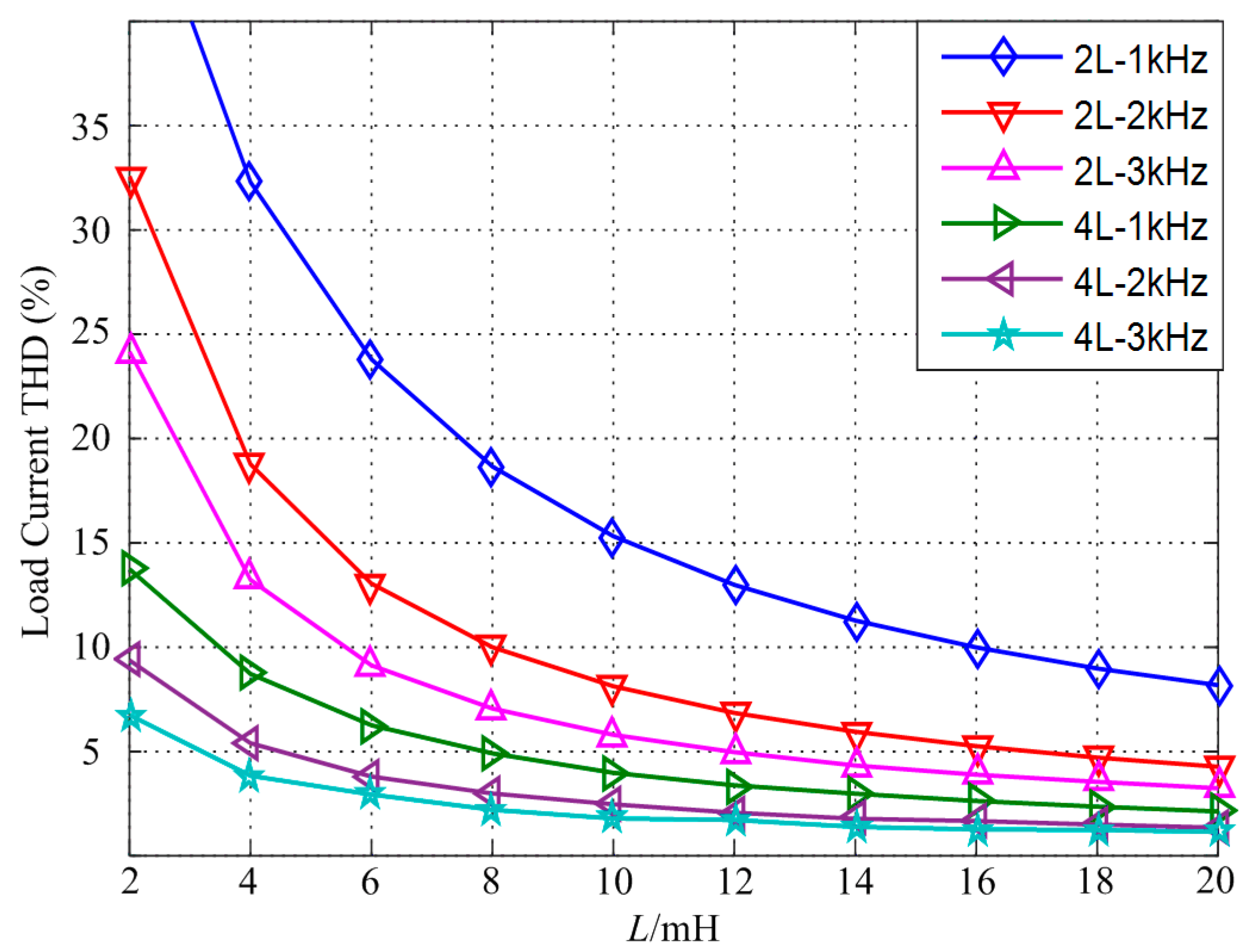
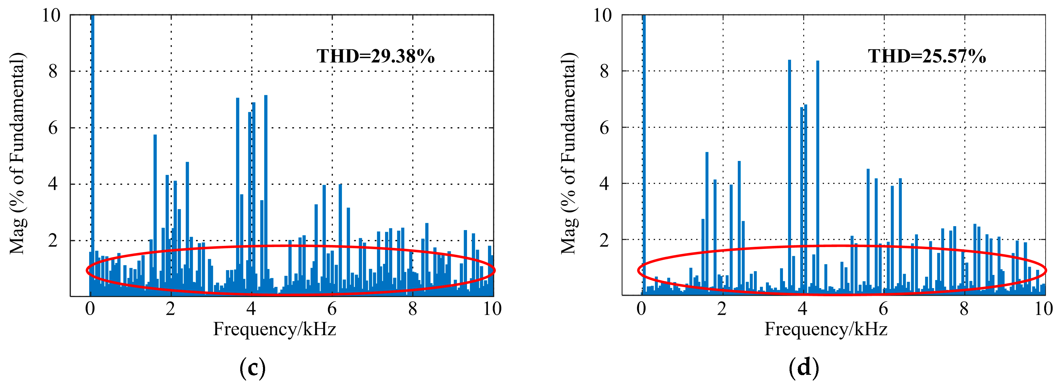
4.3. Comparison with Two-Level Converter

Compared with a 2L converter, the 4L converter can reduce filter requirements and the switching frequencies for the same harmonics. Figure 11 shows the simulated load current total harmonic distortion (THD) of the 4L hybrid converter and the 2L converter with various output inductances and switching frequencies. The current THD of the 4L hybrid converter is much smaller than the 2L converter with the same output inductance and switching frequency. Therefore, the 4L converter can have smaller filter requirements and lower switching frequencies.

4.4. Analysis of the Capacitor Voltage Fluctuations

Figure 12 shows the fluctuations of the FC voltages under different conditions. It can be seen that the FC voltage fluctuations do not change much when m is changing, and the FC voltage fluctuations are almost constant when PF is changing. The reason is that the FC voltages fluctuations are related to both the output levels of the converter and the phase currents. As shown in Table 4, it can be seen that there are effects on the FC voltages when the output levels are only 2 and 1. When m is reduced, the chances of using output level 2 and 1 will increase, so the FC voltages fluctuations may become bigger. However, the phase currents also become smaller when m is reduced, and the FC voltages fluctuations will become smaller as the phase currents become smaller. Therefore, the fluctuation increases with a smaller modulation index but decreases with smaller phase currents. This is also the reason for the FC voltages fluctuations in Figure 8c when the modulation index m is changing. However, when PF is changing, the load impedance is constant, so the phase currents are almost constant. Therefore, there is no effect on the FC voltages fluctuations when PF is changing.
By summarizing the above analysis, it can be concluded that the fluctuations of the FC voltages are actually related to both the output levels of the converter and the magnitude of the phase currents.

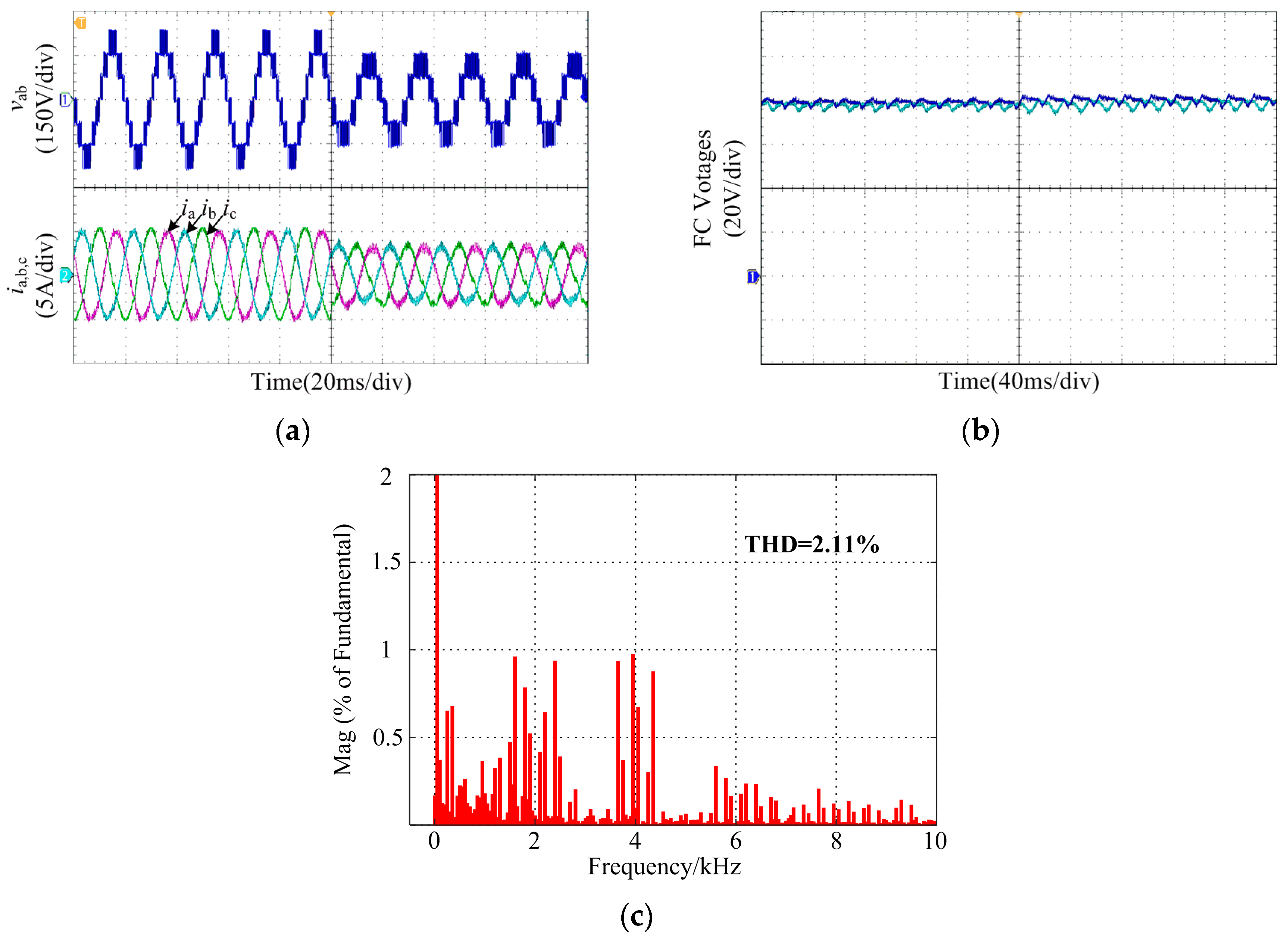
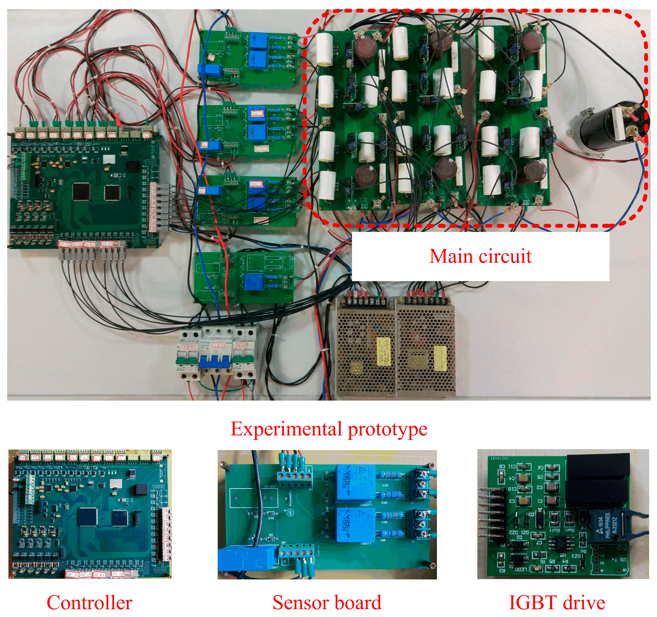
5. Experimental Results

In order to verify the feasibility of the 4L hybrid converter, a down-scaled experimental prototype is built to validate the topology and FC voltage control method. The laboratory prototype is shown in Figure 13. The controller is based on a TMS320F28335 DSP (Texas Instruments, Dallas, TX, USA) and a XC3S400 FPGA (Xilinx, San Jose, CA, USA). The phase currents and the FC voltages are measured by sensors LA 55-P and LV 25-P (LEM, Geneva, Switzerland). The power switches are IGBTs (IKW40N120T2, 1200V/40A, Infineon, Munich, Germany). The parameters are shown in Table 6.
The experimental results are shown in Figure 14, Figure 15 and Figure 16. Figure 14 shows the line voltage under different switching states when the modulation index m = 0.9. Figure 14a is the line voltage when the basic switching states are used. We can see that there are some unreasonable voltage jumps in line voltage. At this moment, the converter has higher switching voltage stress (dv/dt), and the THD of line voltage is 29.38%, as shown in Figure 14c. However, when the adjusted switching states are used, the unreasonable voltage jumps in line voltage almost disappears, as shown in Figure 14b, and the THD of line voltage is reduced to 25.57% as shown in Figure 14d. The harmonics in the red area are significantly decreased, which is the same as the simulation results. Therefore, the experiment results prove that the adjusted switching states can availably decrease the voltage jumps, the switching voltage stress can be effectively reduced, and the performance of line voltage has been improved.
Figure 15 shows the line voltage, the three phase currents, the FC voltages, and the THD of the phase current when m is changed from 0.9 to 0.6. Figure 16 shows the line voltage, the three phase currents and the FC voltages with and without controlling the FC voltages. As shown in the experimental results, the output voltages and currents are as expected, and the FC voltages can always be regulated at the desired value of Vdc/3 = 80 V under different conditions—the same as the simulation results. In addition, the THD of the phase current is 2.11%, as shown in Figure 15a. It shows that the phase current is highly sinusoidal and the harmonics are low. The experimental results can verify the feasibility of the 4L hybrid converter and the effectiveness of the control method, and the phenomena of the undesired voltage jumps can be significantly decreased by using the adjusted switching states, which can effectively reduce the switching voltage stress (dv/dt) and improve the performance of the line voltage. Regarding efficiency, the 4L converter can have a higher efficiency than 2L and 3L converters at high switching frequencies due to a lower switching loss, as proved by Reference [27]. In future, the component parameters of the 4L hybrid converter will be optimized to provide the optimal efficiency.

6. Conclusions

The paper has researched a 4L hybrid converter in detail which combines the FC and T-type topologies. Compared with other four-level converters, the topology is simpler and does not need to control the dc-link capacitor voltages, which reduces the control complexity. However, due to the unequal voltage stress of each switch, it requires high voltage devices for high voltage applications, which may increase the cost of the system. Then, the operations of the converter when the switching states commute are analyzed and the reason for the undesired voltage jumps during the dead-time period is researched in detail. The adjusted switching states which are presented can availably decrease the unreasonable voltage jumps. The switching voltage stress can be effectively reduced and the performance of the converter can be improved by using the adjusted switching states. According to the different effects on the FC voltages with different switching states, the FC voltages can be controlled by selecting the appropriate switching states. Through analyzing the relationship between the FC voltage fluctuations and modulation index and PF, it is revealed that the fluctuations of the FC voltages are actually related to both the output voltage level of the converter and the magnitude of the phase currents. Finally, the simulation and experimental results under the steady state and transient state prove that the topology is feasible, the voltage jumps can be significantly decreased and the voltage stress dv/dt is reduced by using the adjusted switching states. The performance of line voltage has been improved. Meanwhile, the FC voltages can be effectively controlled at the desired value by using the control method.

Author Contributions

C.W. wrote the paper, analyzed the principle and designed the experiments; X.Y. shared his experience and knowledge in advanced multilevel converter; J.Z. shared her experience and knowledge in power electronics; K.W. assisted in completing the experiments; Y.Z. analyzed the simulation data; X.W. helped to perform the analysis with constructive discussions.

Acknowledgments

This work was supported by joint Ph.D. program of “double first rate” construction disciplines of CUMT.

Conflicts of Interest

The authors declare no conflict of interest.

References

  1. Kouro, S.; Malinowski, M.; Gopakunmar, K.; Pou, J.; Franquelo, L.G.; Wu, B.; Rodriguez, J.; Pérez, M.A.; Leon, J.I. Recent advances and industrial applications of multilevel converters. IEEE Trans. Ind. Electron. 2010, 57, 2553–2580. [Google Scholar] [CrossRef]
  2. Gong, Z.; Cui, Q.; Zheng, X.; Dai, P.; Cao, D. An improved inperialist competitive algorithm to solve the selected harmonic elimination pulse-width modulation in multilevel converters. Energies 2018, 11, 3080. [Google Scholar] [CrossRef]
  3. Yang, D.; Yin, L.; Xu, S.; Wu, N. Power and voltage control for single-phase cascaded H-bridge multilevel converters under unbalanced loads. Energies 2018, 11, 2435. [Google Scholar] [CrossRef]
  4. Yuan, X. A new nine-switch non-regenerative four-level rectifier. In Proceedings of the 16th European Conference on Power Electronics and Applications (EPE’ 14-ECCE Europe), Lappeenranta, Finland, 26–28 August 2014. [Google Scholar]
  5. Yuan, X. Derivation of multilevel voltage source converter topologies. In Proceedings of the IECON 2016 42nd Annual Conference on IEEE Industrial Electronics, Florence, Italy, 23–26 October 2016. [Google Scholar]
  6. Holtz, J. Self-communtated inverters with staircase output voltage for large power and high frequency. Siemens Res. Dev. Rep. 1977, 6, 164–171. [Google Scholar]
  7. Schweizer, M.; Kolar, J.W. Design and implementation of a highly efficient three-level T-type converter for low-voltage applications. IEEE Trans. Power Electron. 2013, 28, 899–907. [Google Scholar] [CrossRef]
  8. Aghdam, G.H. Optimised active harmonic elimination technique for three-level T-type inverters. IET Power Electron. 2013, 6, 425–433. [Google Scholar] [CrossRef]
  9. Xu, S.; Zhang, J.; Hang, J. Investigation of a fault-tolerant three-level T-type inverter system. IEEE Trans. Ind. Appl. 2017, 53, 4613–4623. [Google Scholar] [CrossRef]
  10. Li, J.; Englebretson, S.; Huang, A.Q. Reliability comparison for 3L-NPC and 3L-ANPC converters for drives application. In Proceedings of the 2011 IEEE International Electric Machines & Drives Conference (IEMDC), Niagara Falls, ON, Canada, 15–18 May 2011; pp. 271–276. [Google Scholar]
  11. Jiao, Y.; Lee, F.C. New modulation scheme for three-level active neutral-point-clamped converter with loss and stress reduction. IEEE Trans. Ind. Electron. 2015, 62, 5468–5479. [Google Scholar] [CrossRef]
  12. Hu, C.; Holmes, G.; Shen, W.; Yu, X.; Wang, Q.; Luo, F. Neutral-point potential balancing control strategy of three-level active NPC inverter based on SHEPWM. IET Power Electron. 2017, 10, 1943–1950. [Google Scholar] [CrossRef]
  13. Li, J.; Huang, A.Q.; Liang, Z.; Bhattacharya, S. Analysis and design of active NPC (ANPC) inverters for fault-tolerant operation of high-power electrical drives. IEEE Trans. Power Electron. 2012, 27, 519–533. [Google Scholar] [CrossRef]
  14. Burguete, E.; López, J.; Zabaleta, M. New five-level active neutral-point-clamped converter. IEEE Trans. Ind. Appl. 2015, 51, 440–447. [Google Scholar] [CrossRef]
  15. Taallah, A.; Mekhilef, S. Active neutral point clamped converter for equal loss distribution. IET Power Electron. 2014, 7, 1859–1867. [Google Scholar] [CrossRef]
  16. Burguet, E.; López, J.; Zabaleta, M. A new five-level active neutral-point-clamped converter with reduced overvoltages. IEEE Trans. Ind. Electron. 2016, 63, 7175–7183. [Google Scholar] [CrossRef]
  17. Wang, K.; Li, Y.; Zheng, Z.; Xu, L. A novel hybrid-clamped four-level converter. In Proceedings of the 27th Annual Applied Power Electronics Conference and Exposition (APEC), Orlando, FL, USA, 5–9 February 2012; pp. 2442–2447. [Google Scholar]
  18. Wang, K.; Zheng, Z.; Xu, L.; Li, Y. A four-level hybrid-clamped converter with natural capacitor voltage balancing ability. IEEE Trans. Power Electron. 2014, 29, 1152–1162. [Google Scholar] [CrossRef]
  19. Wang, K.; Xu, L.; Zheng, Z.; Li, Y. Voltage balancing control of a four-level hybrid-clamped converter based on zero-sequence voltage injection using phase-shifted PWM. IEEE Trans. Power Electron. 2016, 31, 5389–5399. [Google Scholar] [CrossRef]
  20. Narimani, M.; Wu, B.; Cheng, Z.; Zargari, N.R. A new nested neutral point-clamped (NNPC) converter for medium-voltage (MV) power conversion. IEEE Trans. Power Electron. 2014, 29, 6375–6382. [Google Scholar] [CrossRef]
  21. Narimani, M.; Wu, B.; Cheng, Z.; Zargari, N.R. A novel and simple single-phase modular for the nested neutral-point clamped (NNPC) converter. IEEE Trans. Power Electron. 2015, 30, 4069–4078. [Google Scholar] [CrossRef]
  22. Tian, K.; Wu, B.; Narimani, M.; Xu, D.; Cheng, Z.; Zargari, N.R. A capacitor voltage-balancing method for nested neutral point clamped (NNPC) inverter. IEEE Trans. Power Electron. 2016, 31, 2575–2583. [Google Scholar] [CrossRef]
  23. Hajirayat, A.; Faraji, F.; Birjandi, A.A.M. A novel nested T-type four-level inverter for medium voltage applications. In Proceedings of the 31st International Power System Conference (PSC), Tehran, Iran, 24–26 October 2016. [Google Scholar]
  24. Wei, C.; Yuan, X.; Wu, X.; Zhou, J.; Yuan, Y.; Zhu, Y. A new four-level converter for low and medium voltage applications. In Proceedings of the IECON 2017 43rd Annual Conference on IEEE Industrial Electronics, Beijing, China, 29 October–1 November 2017; pp. 6351–6356. [Google Scholar]
  25. Bahrami, A.; Narimani, M. A sinusoidal pulse width modulation (SPWM) technique for capacitor voltage balancing of nested T-type four-level inverter. IEEE Tran. Power Electron. 2019, 34, 1008–1012. [Google Scholar] [CrossRef]
  26. Mcgrath, B.P.; Holmes, D.G. Multicarrier PWM strategies for multilevel inverters. IEEE Tran. Ind. Electron. 2002, 49, 858–867. [Google Scholar] [CrossRef]
  27. Jin, B.; Yuan, X. Topology, efficiency analysis and control of a four-level π-type converter. IEEE J. Energy Sel. Top. Power Electron. 2018. [Google Scholar] [CrossRef]
Figure 1. The 4L hybrid converter topology.
Energies 12 00698 g001
Figure 2. Six operation states corresponding to six switching states: (a) A; (b) B1; (c) B2; (d) C1; (e) C2; and (f) D.
Energies 12 00698 g002aEnergies 12 00698 g002b
Figure 3. Switching patterns when the switching states commute from A to B1: (a) the basic switching states; (b) the adjusted switching states.
Energies 12 00698 g003
Figure 4. Current paths during dead-time period when the switching states commute from A to B1: (a) the basic switching states; (b) the adjusted switching states.
Energies 12 00698 g004
Figure 5. Procedure of selecting the appropriate switching states for phase x.
Energies 12 00698 g005
Figure 6. Simulation results when m = 0.9: (a) line voltage when the basic switching states are used; (b) line voltage when the adjusted switching states are used; (c) the THD of line voltage when the basic switching states are used; (d) the THD of line voltage when the adjusted switching states are used; (e) phase currents; (f) FC voltages.
Energies 12 00698 g006aEnergies 12 00698 g006b
Figure 7. Simulation results when m = 0.6: (a) line voltage; (b) phase currents; (c) FC voltages.
Energies 12 00698 g007
Figure 8. Simulation results under different m: (a) line voltage; (b) phase currents; (c) FC voltages.
Energies 12 00698 g008
Figure 9. Simulation results with and without controlling FC voltages: (a) line voltage; (b) phase currents; (c) FC voltages.
Energies 12 00698 g009
Figure 10. The performance comparison of the hybrid 4L converter and 4L NNPC: (a) the THDs of the currents under different m when PF = 0.95 and (b) the THDs of the currents under PF when m = 0.9.
Energies 12 00698 g010
Figure 11. Load current THD of the 4L hybrid converter and a 2L converter with various output inductances and switching frequencies.
Energies 12 00698 g011
Figure 12. The FC voltages fluctuations under different conditions.
Energies 12 00698 g012
Figure 13. Experimental prototype.
Energies 12 00698 g013
Figure 14. The line voltage under different switching states: (a) the basic switching states; (b) the adjusted switching states; (c) the THD of line voltage when the basic switching states are used; (d) the THD of line voltage when the adjusted switching states are used.
Energies 12 00698 g014aEnergies 12 00698 g014b
Figure 15. Experimental results under different m: (a) line voltage and phase currents; (b) FC voltages; (c) the THD of phase current.
Energies 12 00698 g015
Figure 16. Experimental results with and without controlling FC voltages: (a) line voltage and phase currents; (b) FC voltages.
Energies 12 00698 g016
Table 1. Comparison of 4L converter topologies.
TopologySwitchesClamping DiodesFlying CapacitorsDC-Link Capacitors
4L-NPC1812-3
4L-FC18-91
4L-HC24-33
4L-NNPC18661
4L hybrid converter18-61
Table 2. Six basic switching states of the converter.
Output LevelVxoTx1Tx2Tx3Tx4Tx5Tx6Switching State
3Vdc110000A
22Vdc/3101100B1
010001B2
1Vdc/3100010C1
001101C2
00000011D
Table 3. Six adjusted switching states of the converter.
Output LevelVxoTx1Tx2Tx3Tx4Tx5Tx6Switching State
3Vdc111000A
22Vdc/3101100B1
011001B2
1Vdc/3100110C1
001101C2
00000111D
Table 4. Conditions of the FCs under various switching states and phase currents.
Output LevelPhase Current, ixCx1Cx2Switching State
3-No effectNo effectA
2>0ChargingNo effectB1
<0DischargingNo effect
>0DischargingDischargingB2
<0ChargingCharging
1>0ChargingChargingC1
<0DischargingDischarging
>0No effectDischargingC2
<0No effectCharging
0-No effectNo effectD
Table 5. Simulation parameters.
ParametersValues
DC Voltage3300 V
Flying Capacitor1000 μF
Output Frequency50 Hz
Load Inductance7.5 mH
Load Resistance20 Ω
Switching Frequency2 kHz
Dead-time4 μs
Table 6. Experimental parameters.
ParametersValues
DC Voltage240 V
Flying Capacitor1000 μF
Output Frequency50 Hz
Load Inductance7.5 mH
Load Resistance20 Ω
Switching Frequency2 kHz
Dead-time4 μs

