Article

A New Hybrid Inductor-Based Boost DC-DC Converter Suitable for Applications in Photovoltaic Systems

Applied Electronics Department, Politehnica University Timişoara, 300006 Timișoara, Romania
*
Author to whom correspondence should be addressed.
Energies 2019, 12(2), 252; https://doi.org/10.3390/en12020252
Submission received: 18 December 2018 / Revised: 9 January 2019 / Accepted: 10 January 2019 / Published: 15 January 2019

Abstract

:
A new hybrid step-up converter suitable in applications where large conversion ratios are needed is presented. The topology is still simple, containing only one transistor and three diodes. A detailed dc and ac analysis is performed and all design equations are provided. Compared to other topologies of the same type, the proposed converter exhibits lower or equal current and voltage stresses. A state space model is provided including the conduction losses and based on it the audio susceptibility and the control to output function are derived. As the converter is still of second order with the control to output transfer function exhibiting a right half plane zero, controller design is practically the same like in a Boost topology. It is shown how the proposed converter can be used in a photovoltaic system for performing the maximum power point tracking algorithm using the perturb and observe method. All theoretical considerations are verified through simulation and finally validated by practical experiments.

1. Introduction

In the context of today’s energy and pollution crisis [1,2], renewable energy sources have gained increasingly more interest [2,3,4,5]. As defined, these sources are naturally available on a practical infinite timescale, are easily accessible in most geographic locations and climate conditions and have no impact on the environment during the energy harvesting and its distribution [5]. There are several types of renewable energies, out of which the “green production” of electrical energy particularly stands out because it is the most used in many applications. Researchers have granted it a special interest due to the several advantages that it offers [1,2,3,4,5]. Firstly, after the electrical energy is produced, it can be easily transported over long distances thus making the production and consumption positions geographically independent. Secondly, electrical energy has a wide variety of applications from powering home appliances to heating/cooling, industrial transportation and recently personal transportation [4,5,6,7,8,9]. Additionally, another advantage of electrical renewable energy is the multitude of available production methods, out of which the following can be enumerated: photovoltaic (PV) panels, wind-turbines, hydro-turbines and fuel cells [2,3,4,5]. These provide the possibility to exploit specific local advantages and still be able to unify the principally different sources into a single green electrical smart grid [9,10,11]. The interest for PV energy has grown exponentially in the recent years as a result of the improving technology which now offers better efficiency, lower cost and reliability. Other advantages are the scalability and the ability to connect PV matrices to the public power grids with the option of selling any available energy excess, because the electromagnetic energy is hard to be efficiently stored. The challenge in the case of a home standalone or on-grid connected PV system is the low voltages obtained from the PV modules [12,13,14,15,16,17]. To increase the voltage, the PV modules should be either connected in series to meet these application requirements, or, more conveniently, to use a step-up DC-DC converter. In our days, a large number of power conversion systems are based on DC-DC converters with high voltage boost capability. Traditionally, when a high step-up in voltage is needed two classical Boost converters are cascaded. A review of non-isolated high step-up DC-DC converters used in renewable energy systems, together with the advantages and disadvantages of these converters, are presented in [18,19,20,21,22,23,24,25]. For increasing the voltage gain the authors in [26,27,28,29], are using a transformer. Other solutions that are found in the literature consist of different families of multi-input converters [30], multiphase converters [31,32,33,34,35], quadratic converters [36,37,38,39], stacked step-up converters [40,41] or switched-capacitor/switched-inductor structures for getting transformerless hybrid DC-DC pulse width modulated (PWM) converters [42,43]. Also, in [44,45,46] a high step-up DC-DC converter that uses at least one pair of coupled inductors is presented.
In this paper, inspired by the topology presented in [42], the authors, developed a new hybrid converter structure with coupled inductor that exhibits a higher step-up conversion ratio than the topology presented in [42]. The steps for developing the structure of the new topology, together with the operation principle in Continuous Conduction Mode (CCM), the corresponding dc analysis, the main equations and the theoretical waveforms are presented in Section 2. In Section 3 an ac analysis is performed regarding the inductor currents and capacitor voltage ripples and the CCM operation condition is derived. Taking into account the conduction losses, the converter static conversion ratio, the small-signal control to output transfer function and the input to output transfer function using the state space analysis are derived in Section 4. A design example is provided in Section 5, while in Section 6 the theoretical considerations are verified through simulation. In order to practically validate all the concepts, Section 7 is devoted to the experimental results. For proving the suitability of the new structure in PV applications, a PV system based on the proposed converter is presented in Section 8, with emphasis on its behavior to variations of irradiance and temperature. A maximum power point tracking (MPPT) algorithm is implemented using the Perturb and Observe (P&O) method and the whole system is finally validated both by simulations and experiments. Some conclusions and comments are drawn in the Section 9.

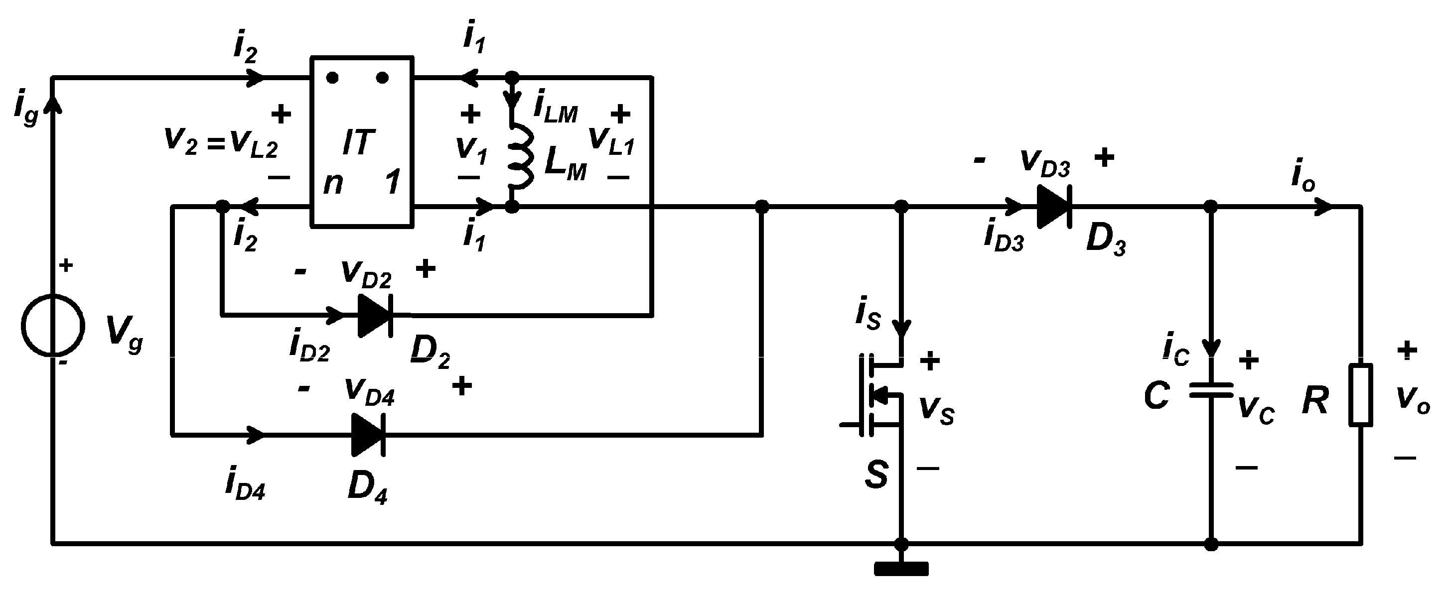
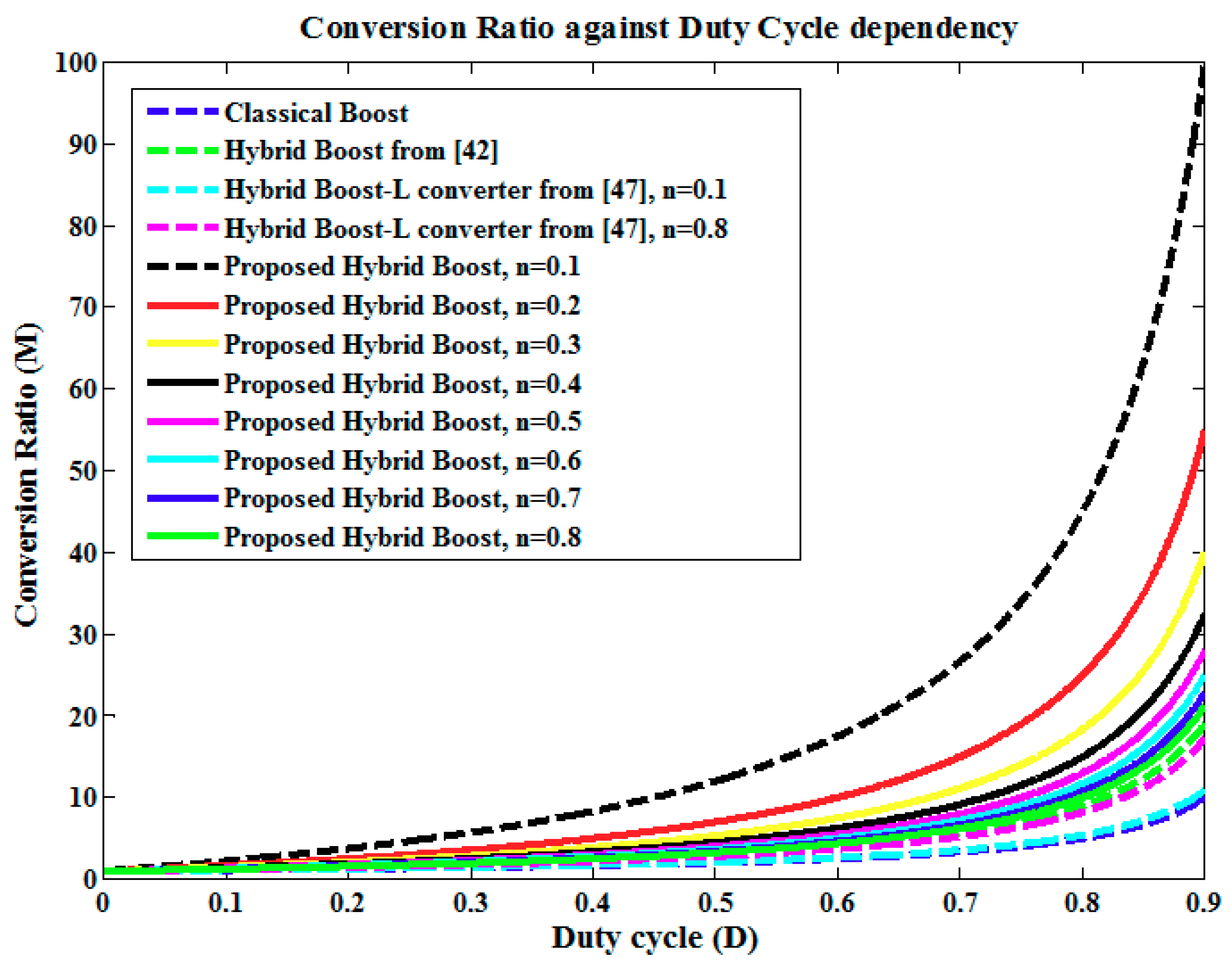
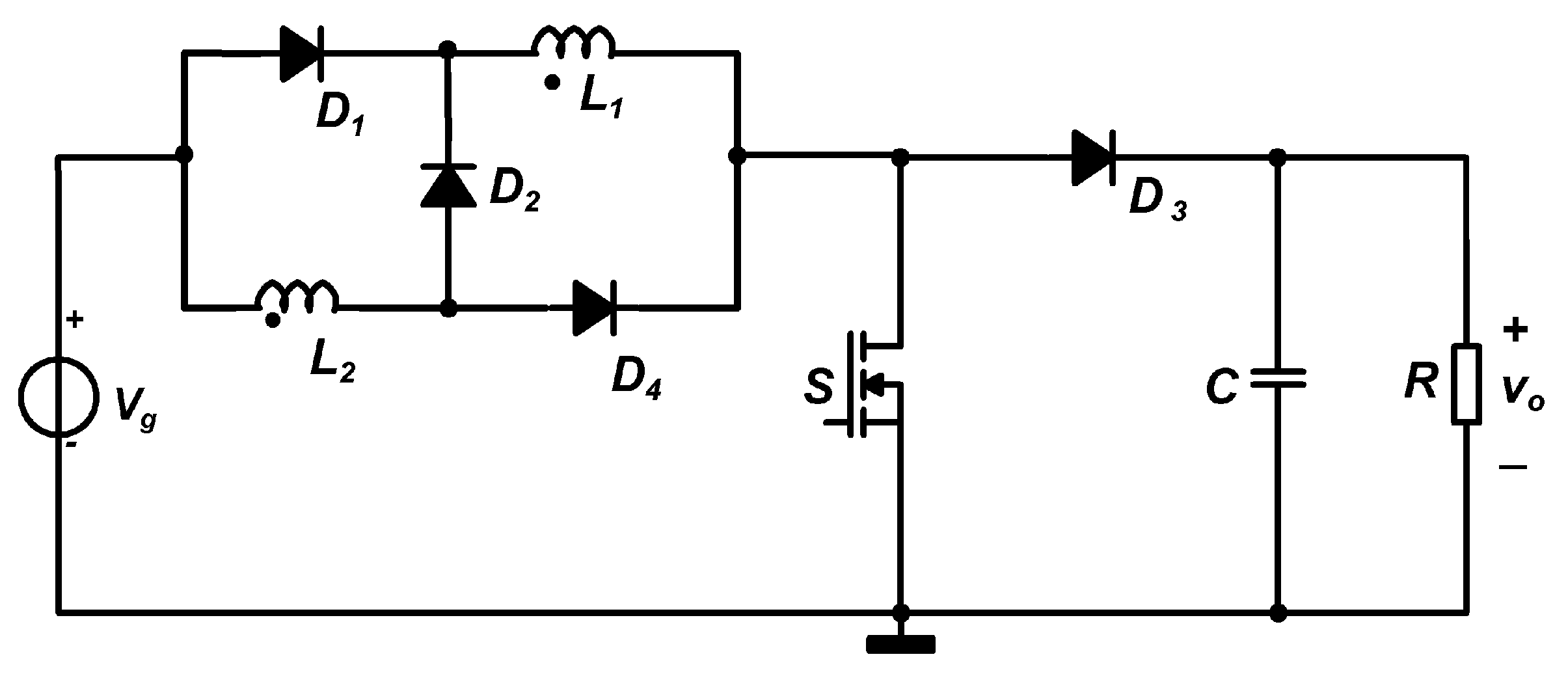
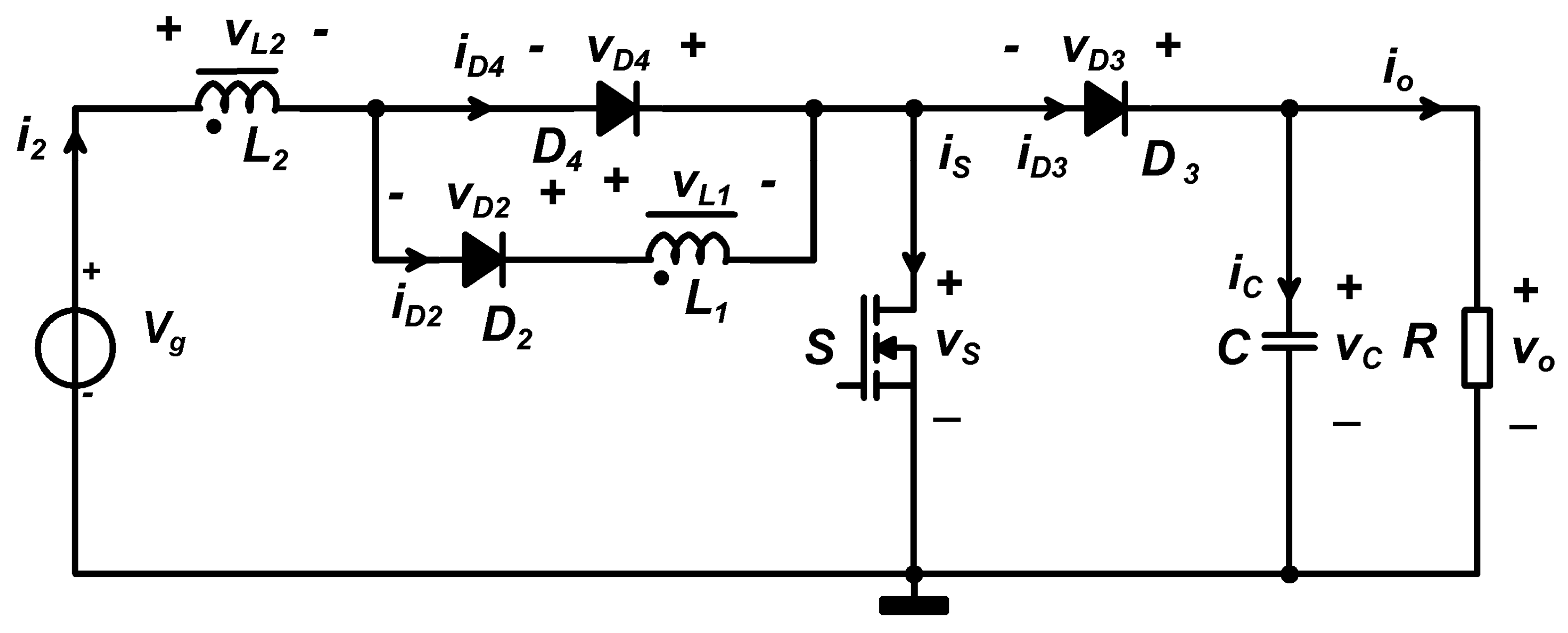
2. DC Analysis of the Proposed Hybrid Inductor-Based Boost Converter

In developing the new proposed converter the authors were inspired by the step-up hybrid Boost-L converter with switching structure Up3 [42], reproduced in Figure 1. The first step was to couple the inductors, resulting in an interesting topology. The second remark is that if the transformer ratio is less than unity, diode D1 is always off. Consequently, it was removed from the circuit. With one diode less, and also one core less due to the coupling of the inductors, the circuit becomes simpler and cheaper than the topologies presented in [42,43]. The resulted new proposed converter is presented in Figure 2 and it consists of one active switch, three passive switches, two coupled inductors and one capacitor at the output. The dc analysis is performed for CCM operation with respect to diodes D2, D3, and D4. In deriving the static conversion ratio an ideal converter is presumed, that is all devices are lossless and perfect coupling of the inductors is assumed. Typically, the assumption of small ripple state variables is considered for CCM operation [47,48,49,50]. When not explicitly specified, capitals will denote dc values. The switching frequency and the corresponding switching period will be denoted by fs and Ts respectively. A PWM signal is used to drive the transistor and the transistor duty cycle will be denoted by D.
Because the inductors are perfectly coupled, in order to perform the dc analysis a simplified schematic is drawn in Figure 3, where the coupled inductors are modeled by an ideal transformer (IT) together with a magnetizing inductor, LM. Let the ideal transformer ratio be denoted by n. In our approach the magnetizing inductor is connected between the drain of the transistor and the cathode of D2. Therefore the value for LM equals L1.
In Figure 4a,b the two circuits corresponding to the two topological states are depicted, according to the conduction state of the power transistor and diodes. In the first topological state, from 0 to D∙Ts, transistor S and diode D4 are on. The other two diodes, D2 and D3, are off because they are reversely biased. In the second topological state, from D∙Ts to Ts, transistor S and diode D4 are off and diodes D2 and D3 are on, as they perform the freewheel operation. The main waveforms related to the active and passive components are depicted in Figure 5 and Figure 6. The transistor switching function denoted by q is taken as reference in each figure. Using the notations from Figure 3, the ideal transformer equations are:
v 2 = n · v 1
i 1 + n · i 2 = 0
The static conversion ratio of the converter can be determined by applying the voltage-second balance on the magnetizing inductor. In the first topological state the voltage across the magnetizing inductor can be written as follows:
v L M _ O N = V g n
While in the second topological state the same voltage is:
v L M _ O F F = V g V C 1 + n
Hence volt-second balance equation is:
D · ( V g n ) + ( 1 D ) · V g V C 1 + n = 0
The voltage across the magnetizing inductor is positive in the on state and negative in the off state as results from Equations (3) and (4) and can be seen in Figure 5.
The dc voltage across the output capacitor is equal to the output voltage and results from Equation (5):
V C = V o = D + n n · ( 1 D ) · V g
Therefore, the ideal static conversion ratio M of the new hybrid inductor-based Boost converter can be obtained from Equation (6):
M = D + n n · ( 1 D )
Examining the static conversion ratio it can be observed the output voltage is higher than the input voltage, the converter being of step-up type. The dependency of the static conversion ratio on the duty cycle, when n is a parameter and n < 1, is presented in Figure 7. From Figure 7 and according to Equation (7), it is obvious that the output voltage of the proposed hybrid Boost converter with coupled inductors is suitable especially for applications where the difference between the input voltage and the output voltage is high as it still requires moderate duty cycles. This static conversion ratio is even higher than that of the hybrid Boost converter proposed in [42] or the hybrid Boost converter with coupled inductors in [47], at the same duty cycle, provided if the transformer ratio is less than unity. If n = 1, the static conversion ratio is (1 + D)/(1 − D), the same as for the converter proposed in [42,47].
The charge balance principle for the output capacitor is used in order to calculate the dc magnetizing inductor current:
D · ( V C R ) + ( 1 D ) · ( I L M · 1 n + 1 V C R ) = 0
By solving Equation (8) the dc magnetizing inductor current, ILM, is:
I L M = n + 1 1 D · V C R
The right hand side of Equation (9) can be written only in terms of static conversion ratio, output voltage and output power by expressing the duty cycle from Equation (7), taking into account that VC = Vo and R = Vo2/Po. The same approach will be used for the other stresses. For the dc magnetizing current, the final result is:
I L M = P o · ( M · n + 1 ) V o

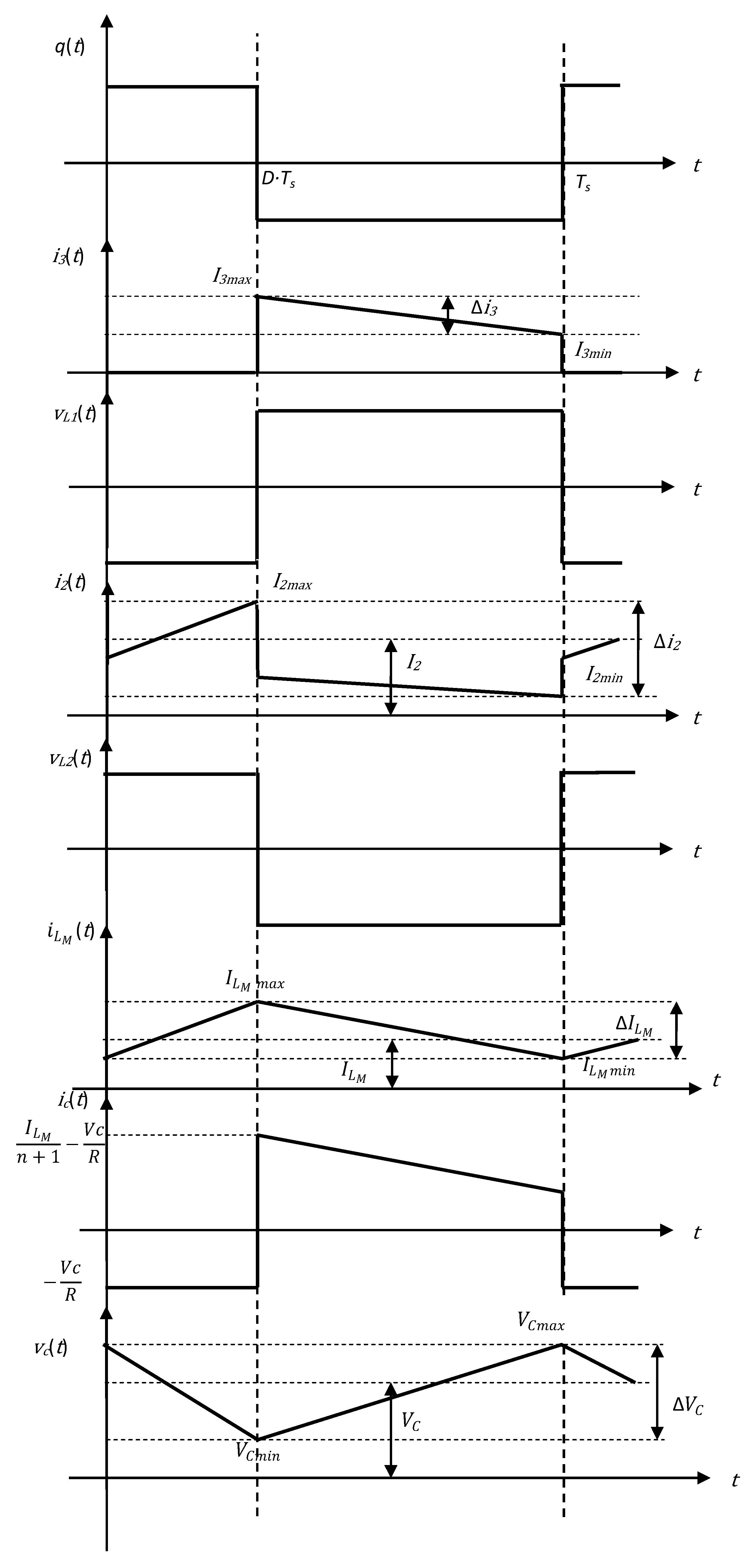
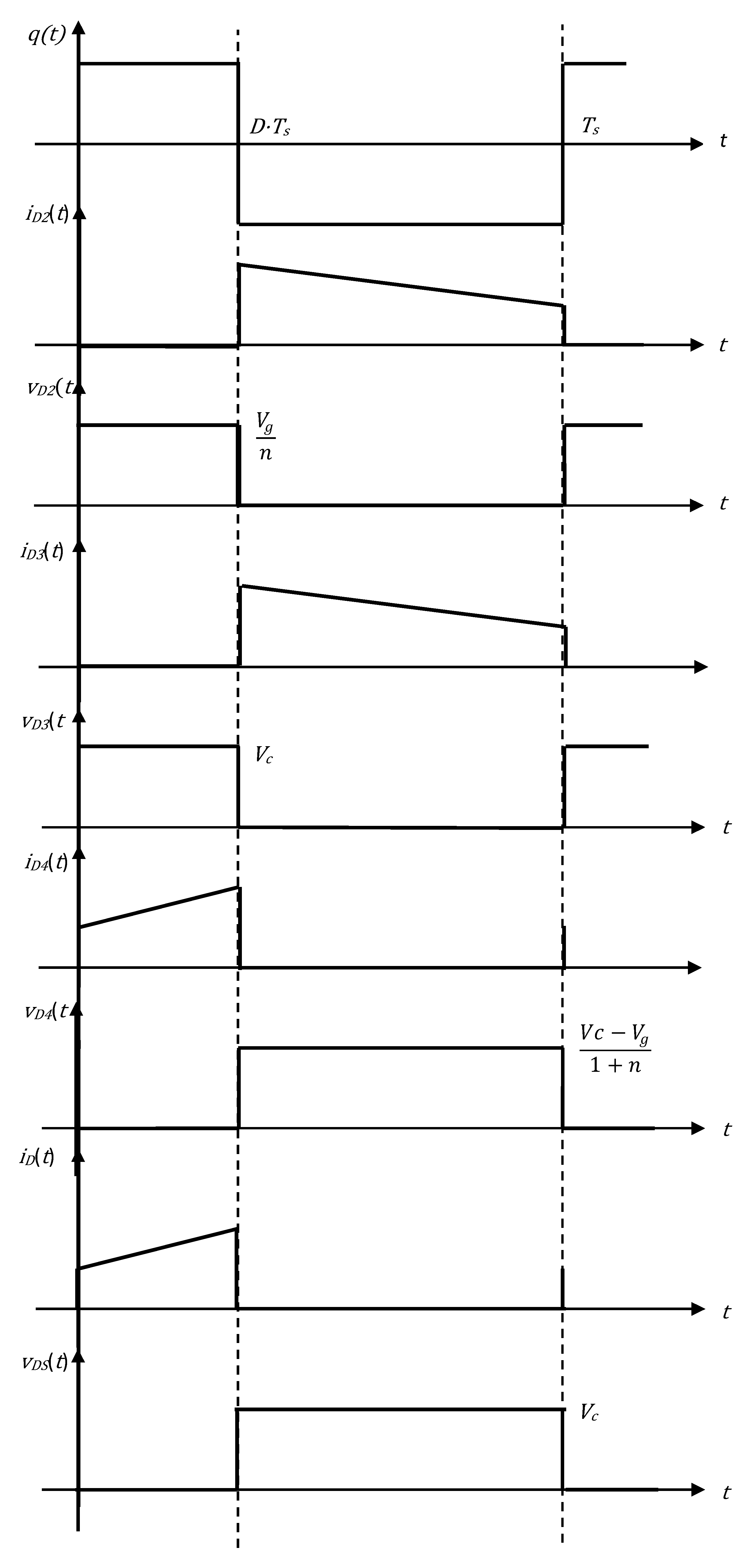
3. Device Stresses and Ripples Calculation

The current and voltage stresses related to the semiconductors are required in the design process. From the second topological state, the maximum transistor voltage stress across switch S is calculated. In this state the diodes D2 and D3 conduct and the transistor is placed across the output voltage source:
V S = V C = D + n n · ( 1 D ) · V g
This also can be rewritten only in terms of static conversion ratio and input voltage as:
V S = V C = M · V g
The dc transistor current stress is calculated from the first topological state taking into account that current ILM/n flows through it:
I S = D · I L M n = D · ( n + 1 ) · ( D + n ) n 2 · ( 1 D ) 2 · V g R
or, if ILM is substituted from Equation (10) and the duty cycle is expressed from Equation (7), the result is:
I S = P o · ( M 1 ) V o
The voltage stress across diode D4 is calculated from the second topological state:
V D 4 = V C V g 1 + n
Equation (15) can be rewritten in terms of input voltage and static conversion ratio, with the help of Equation (6):
V D 4 = V g · ( M 1 ) ( 1 + n )
The dc current through diode D4 is equal to the dc current flowing through switch S:
I D 4 = D · I L M n = D · ( n + 1 ) · ( D + n ) n 2 · ( 1 D ) 2 · V g R
or, in terms of output power, static conversion ratio and output voltage can be written as:
I D 4 = P o · ( M 1 ) V o
From the first topological state the voltage stress across diode D2 is equal to:
V D 2 = V g n
The dc current through diode D2 can be found from the second topological state and by replacing ILM with the formula from Equation (9), yielding:
I D 2 = ( 1 D ) · I L M n + 1 = ( D + n ) n · ( 1 D ) · V g R
or, if ILM is replaced from Equation (10) and the duty cycle is expressed from Equation (7), it can be rewritten as:
I D 2 = P o V o
For diode D3 the voltage stress can be obtained from the first topological state:
V D 3 = V C = D + n n · ( 1 D ) · V g
that can also be written as:
V D 3 = V C = M · V g
The dc current through diode D3 is equal to the dc current through the diode D2:
I D 3 = ( 1 D ) · I L M n + 1 = ( D + n ) n · ( 1 D ) · V g R
or, using Equation (21):
I D 3 = P o V o
The peak to peak magnetizing current ripple can be written as:
Δ i L M = D · V g L M · f s · n
When the diodes D2 and D3 are on, the current flowing through them equals iLM/(n + 1).When the diode D4 is on the current flowing through it is equal to iLM/n. This means that CCM operation condition is the same for all diodes and it requires that the minimum magnetizing inductor current to be positive. From Equations (9) and (26) the CCM operation condition for diodes D2, D3 and D4 is the same:
2 · L M · f s R D · ( 1 D ) 2 ( n + D ) · ( n + 1 )
If the duty cycle is expressed from Equation (7) and taking into account that R = Vo2/Po, the condition becomes:
2 · L M · f s · P o V o 2 M 1 M · ( M · n + 1 ) 2
The peak-to-peak output voltage ripple is:
Δ V o = Δ V C = V C · D R · C · f s = V g R · C · f S · D · ( n + D ) n · ( 1 D )
The right hand side of Equation (29) can be also written only in terms of static conversion ratio, output voltage, output power, transformer ratio, switching frequency and capacitor value:
Δ V o = Δ V C = P o V o · C · f S · n · ( M 1 ) M · n + 1
Equations (28) and (30) can be used for designing the magnetizing inductor and the output capacitor, imposing the ripples to be lower than a specific threshold. From Equation (28) the minimum necessary magnetizing inductor is:
L M min = ( M 1 ) · V o 2 2 · M · ( M · n + 1 ) 2 · f s · P o
From Equation (30) the minimum output capacitor results in:
C min = P o V o · Δ V o · f S · n · ( M 1 ) M · n + 1
The main voltage and current stresses of the proposed hybrid inductor-based Boost converter are presented in the sixth column of Table 1. As with given input voltage, output voltage and load, these stresses are duty cycle independent, there is one degree of freedom in the design. Usually the duty cycle is chosen to a reasonable value and from the static conversion ratio the transformer turn ratio n is calculated. With LM and n known, the values of the two coupled inductors are immediately available as: L1 = LM, and L2 = n2LM.
To have a comprehensive comparison between different step-up converters supplied by the same input voltage Vg and delivering the same output voltage Vo, that is providing the same conversion ratio M, at the same output power Po to the same load R are analyzed and the results are presented in Table 1. The converters included in the comparison are the following: the first one is the classical Boost converter [50], the second one is the hybrid Up1 from [42], that is a converter with a switching structure formed by two diodes and two capacitors, the third one is hybrid Up3, the converter that the new structure was developed from, proposed in [42] and that can also be found in [43]. The fourth one is another hybrid Boost structure with coupled inductors from [47,51], and the last one is the hybrid inductor-based Boost converter proposed by the authors in this paper. The latter uses only one transistor, three diodes, a capacitor at the output and one magnetic core for the coupled inductors, being a second order converter that is easy to control, like the classical Boost and hybrid Boost-L from [47]. The other two converters, Hybrid Up1 and Hybrid Up3, are third order converters.
For a transformer ratio less than 1, the static conversion ratio of the proposed topology, at the same duty cycle D, is higher than that of all the compared converters, without being quadratic and having the same voltage stress across the switch and diode like the classical, Hybrid Up3 [42] and Hybrid Boost-L [47]. When 1 < M < 2, the switch current stress in the proposed converter is lower than that of a classical Boost, while for M > 2 it becomes higher. The diodes current stresses are the same for all compared topologies.

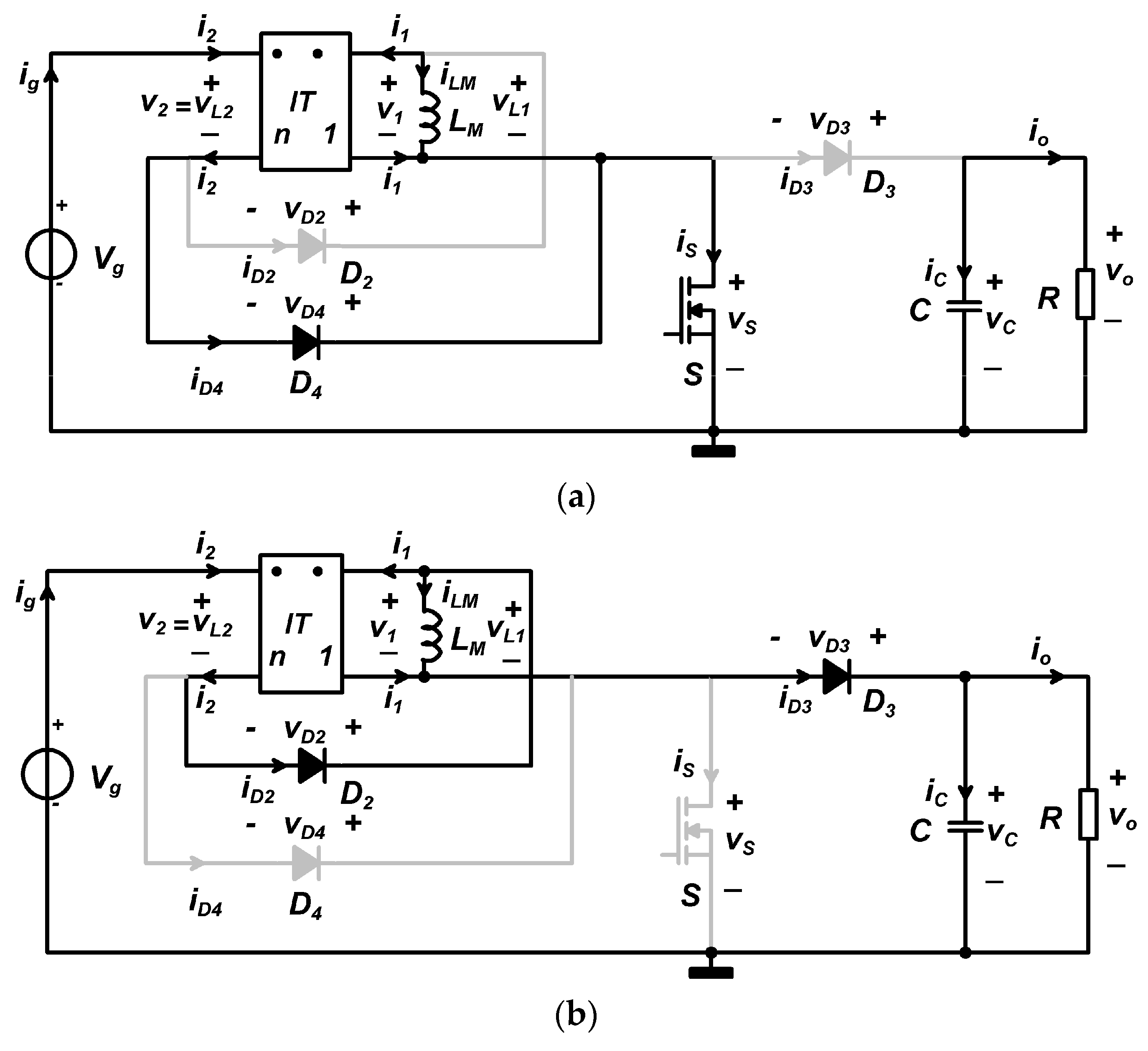
4. State Space Analysis and Model with Lossy Elements

4.1. State Space Analysis

To study the converter dynamics the state space approach is used for the proposed ideal inductor-based Boost converter. Defining the state vector x = [ i L M v C ] , the input vector u = [ v g ] , and output vector y = [ v o ] , the state matrices for the first topological state are:
A 1 = [ 0 0 0 1 R · C ] ;
B 1 = [ 1 n · L M 0 ] ;
E 1 = [ 0 1 ] ;
F 1 = [ 0 ] ;
For the second topological state the state matrices are:
A 2 = [ 0 1 ( n + 1 ) · L M 1 ( n + 1 ) · C 1 R · C ] ;
B 2 = [ 1 ( n + 1 ) · L M 0 ] ;
E 2 = [ 0 1 ] ;
F 2 = [ 0 ] ;
The static conversion ratio was symbolically computed in MATLAB (R2011a, MathWorks, Natick, MA, USA) [52], to check the validity of the previous calculations. The formula used to find the static conversion ratio is [53]:
M = F D E D · A D 1 · B D
where:
{ A D = D · A 1 + ( 1 D ) · A 2 B D = D · B 1 + ( 1 D ) · B 2 E D = D · E 1 + ( 1 D ) · E 2 F D = D · F 1 + ( 1 D ) · F 2
After computing in MATLAB, the resulted static conversion ratio is:
M = D + n n · ( 1 D )
the same with that in Equation (7).
The small signal transfer functions can be obtained after averaging and linearization of the switched equations [53]. The control to output transfer function G c ( s ) = V o ( s ) ^ d ( s ) ^ is:
G c ( s ) = V g · n + 1 n · 1 ( 1 D ) 2 · 1 L M R · ( D + n ) · ( n + 1 ) ( 1 D ) 2 · s 1 + L M R · ( n + 1 ) 2 ( 1 D ) 2 · s + L M · C · ( n + 1 ) 2 ( 1 D ) 2 · s 2
and the audiosusceptibility, G g ( s ) = V o ( s ) ^ V g ( s ) ^ , has the formula:
G g ( s ) = D + n n · ( 1 D ) 1 + L M R · ( n + 1 ) 2 ( 1 D ) 2 · s + L M · C · ( n + 1 ) 2 ( 1 D ) 2 · s 2
This dynamic model can be used for designing the feedback loop. It can be remarked that both transfer functions are of second order and the control to output transfer function exhibits a zero in the right half plane. From this point of view the behavior is similar to that of a classical Boost converter and therefore the controller will be designed exactly with the same procedure, for example using a third order error amplifier [54].

4.2. Model with Lossy Elements

This model is based on more accurate modeling of converter components, considering the effect of conduction losses. The equivalent circuit of the converter with parasitic elements is presented in Figure 8 and the lossy elements that are considered are the transistor on resistance RON and the forward voltage drops for the diodes VD2, VD3 and VD4.
According to the operating principle of the converter, the voltages across the magnetizing inductor in the ON and OFF states are:
v L M _ O N = n · V g R O N · I L M n · V D 4 n 2
v L M _ O F F = V D 2 V D 3 + V g V C n + 1
and applying volt-second balance principle it results that:
D · n · V g R O N · I L M n · V D 4 n 2 + ( 1 D ) · ( V D 2 V D 3 + V g V C n + 1 ) = 0
Solving for VC in MATLAB using symbolic calculation, the output voltage of the converter with conduction losses is:
V c = n + D n · ( 1 D ) · V g V D 2 V D 3 ( n + 1 ) · D n · ( 1 D ) · V D 4 1 + ( n + 1 n ) 2 · D ( 1 D ) 2 · R O N R

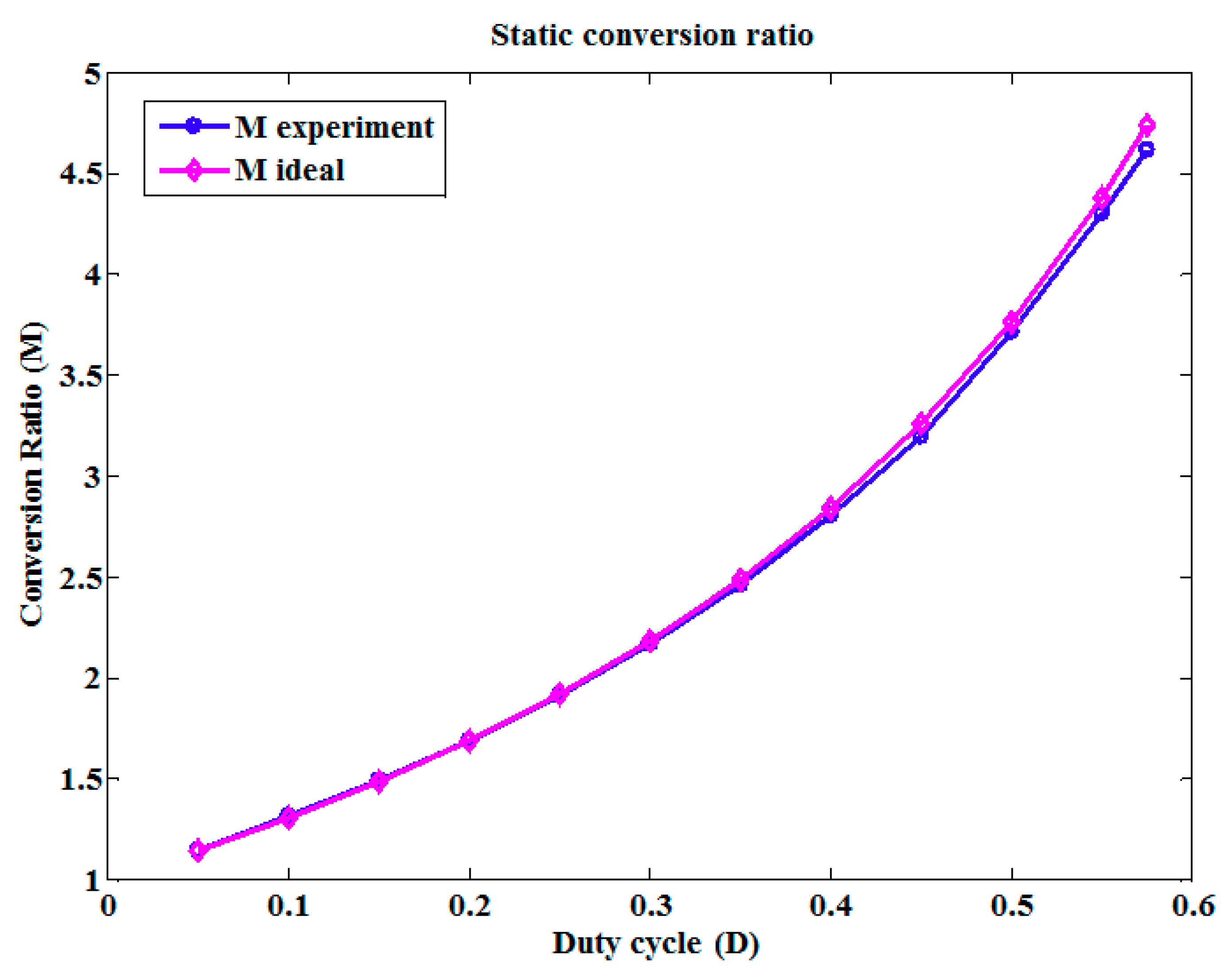
5. Design Example of the Proposed Converter

The proposed converter is used in a PV panel system to perform the MPPT. Therefore the design specifications will be determined by the specifications of the PV module. The equations used for designing the magnetizing inductor and output capacitance are Equations (31) and (32), respectively. To calculate the voltage and current stresses across the semiconductors, Equations (11)–(25) will be used. For experiments the authors used two PV modules connected in series in order to increase the input voltage. The PV module type was MWG-20 from the company MW GREEN POWER, with the following parameters for a PV module:
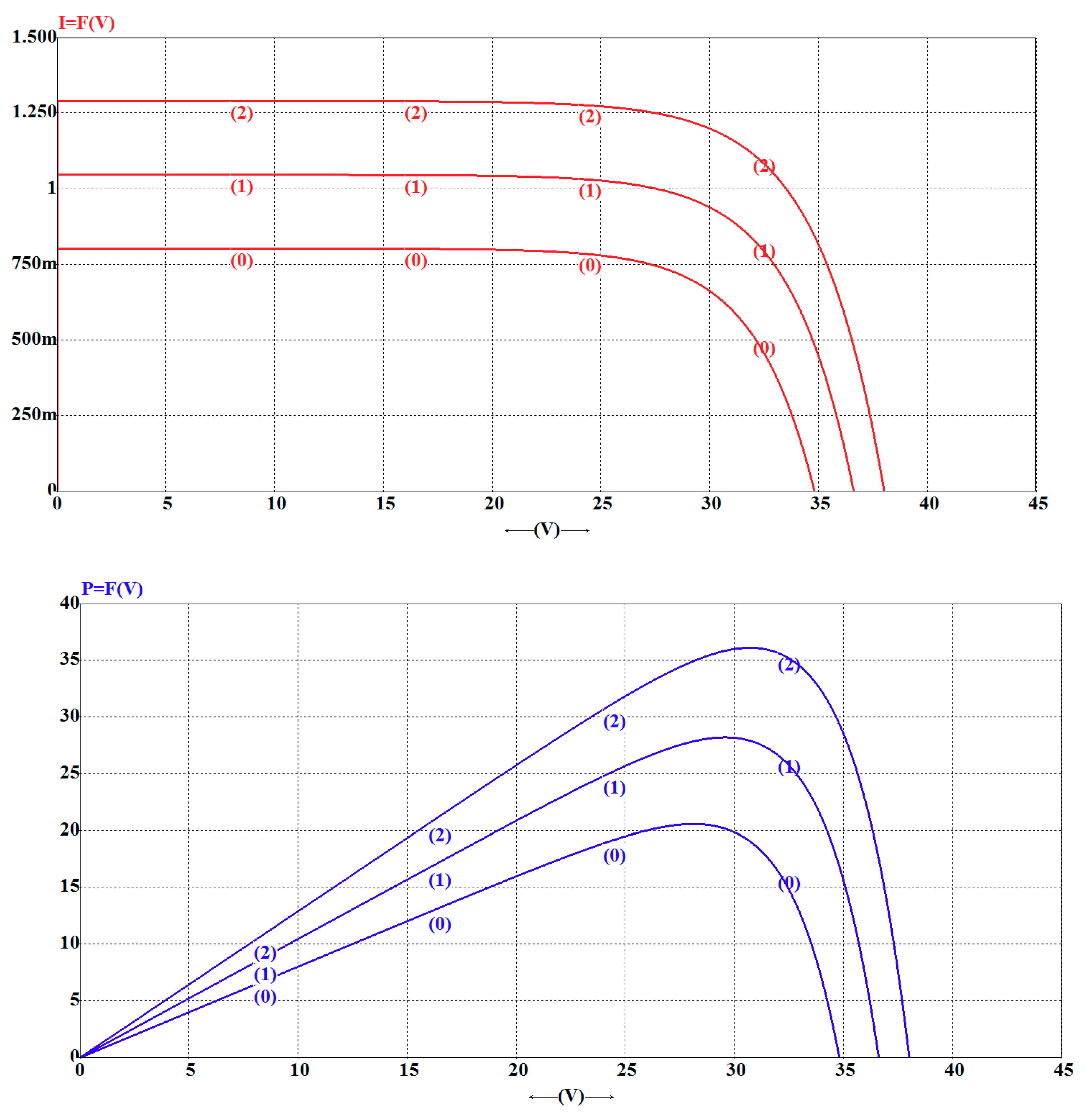
  • Peak power: Pmax = 20 W
  • Maximum power point current: Imp = 1.14 A
  • Maximum power point voltage: Vmp = 17.49 V
  • Short circuit current: Isc = 1.22 A
  • Open circuit voltage: Voc = 21.67 V
These values are obtained in standard test conditions of solar irradiance and temperature: G = 1000 W/m2 and T = 25 °C. As a result of connecting two PV modules in series the following requirements were obtains:
  • The input voltage range was between: Vg = 30 ÷ 35 V
  • Maximum output power: Po = 40 W
  • Switching frequency: fs = 100 kHz
  • Output voltage: Vo = 120 V
Consequently, the static conversion ratio M = Vo/Vg will be between [3.42, 4]. Choosing a duty cycle of 0.5 for the middle of the static converter range, using Equation (7), the necessary transformer turns ratio is found:
n = D M · ( 1 D ) 1
Using Equation (50) the transformer turn ratio resulted to be 0.567 and the calculated duty cycle range resulted between 0.46 and 0.52, which is a very convenient one. For the practical prototype a resistive load of 432 Ω was used. Imposing the inductor current ripples given by Equation (26), the calculated inductor value was LM = 2 mH. The value of LM will be equal to the value of L1, so LM = L1 = 2 mH, and L2 = n2LM = 644 μH. The output capacitor was designed based on Equation (30), imposing the voltage ripple to be 1% of its dc value. A value of C = 10 μF is chosen. According to Equations (12) and (13), the transistor voltage stress is Vs = 120 V and its dc current is IS ~ 1 A. The highest stresses for diodes are a reverse voltage of VD = 120 V calculated with Equation (23) and the dc current ID ~ 1 A, given by Equation (18).

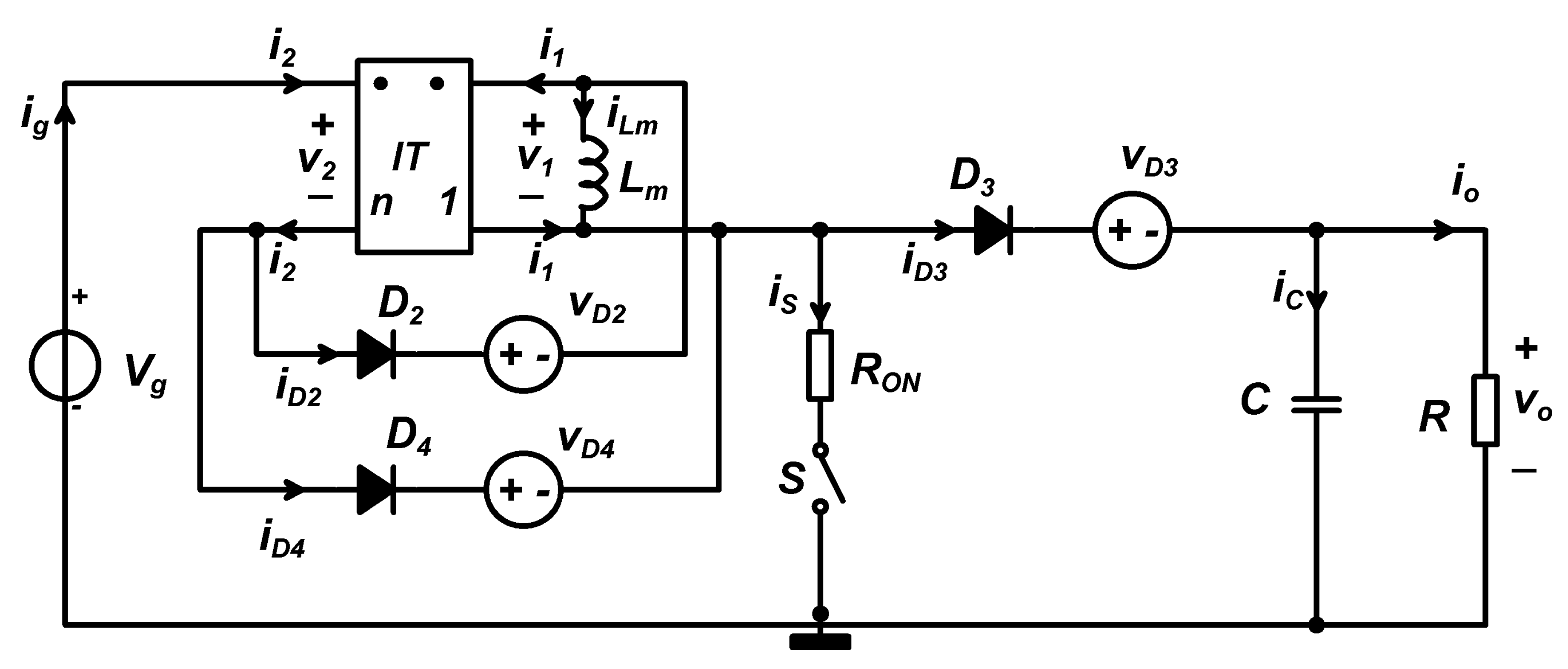
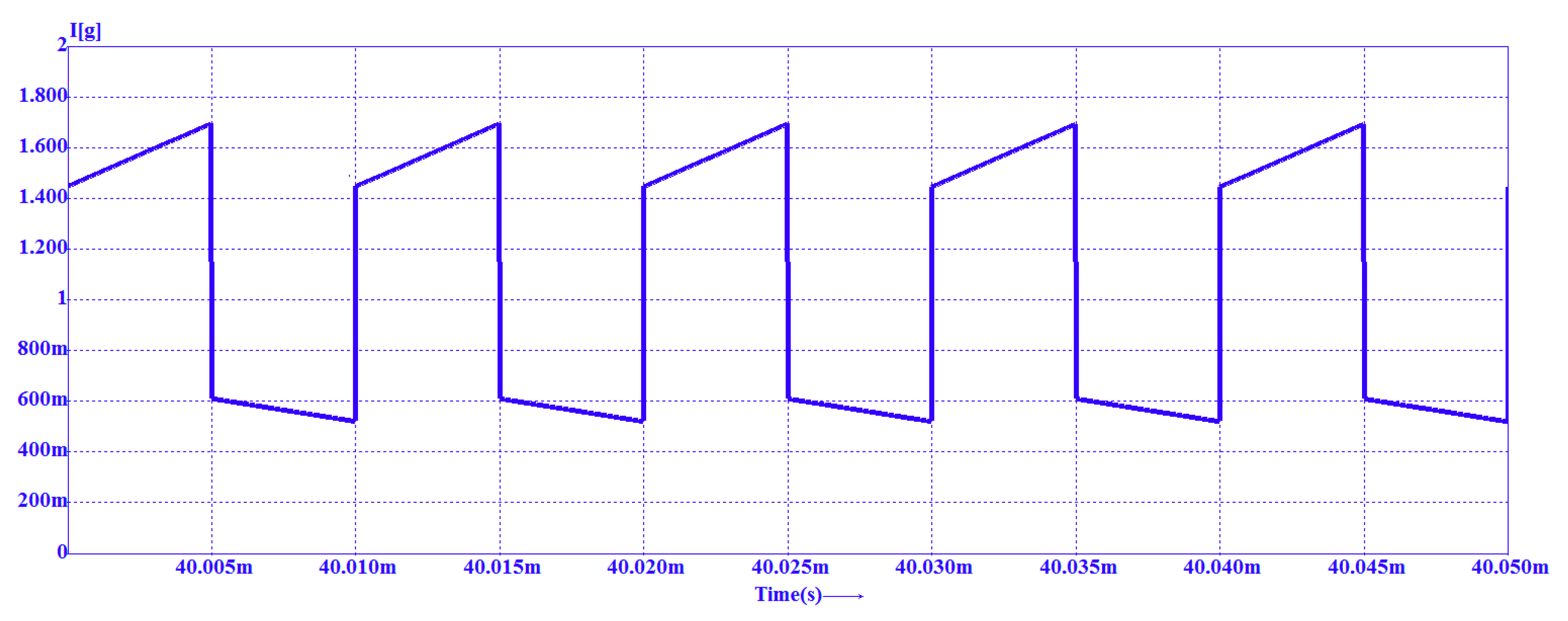
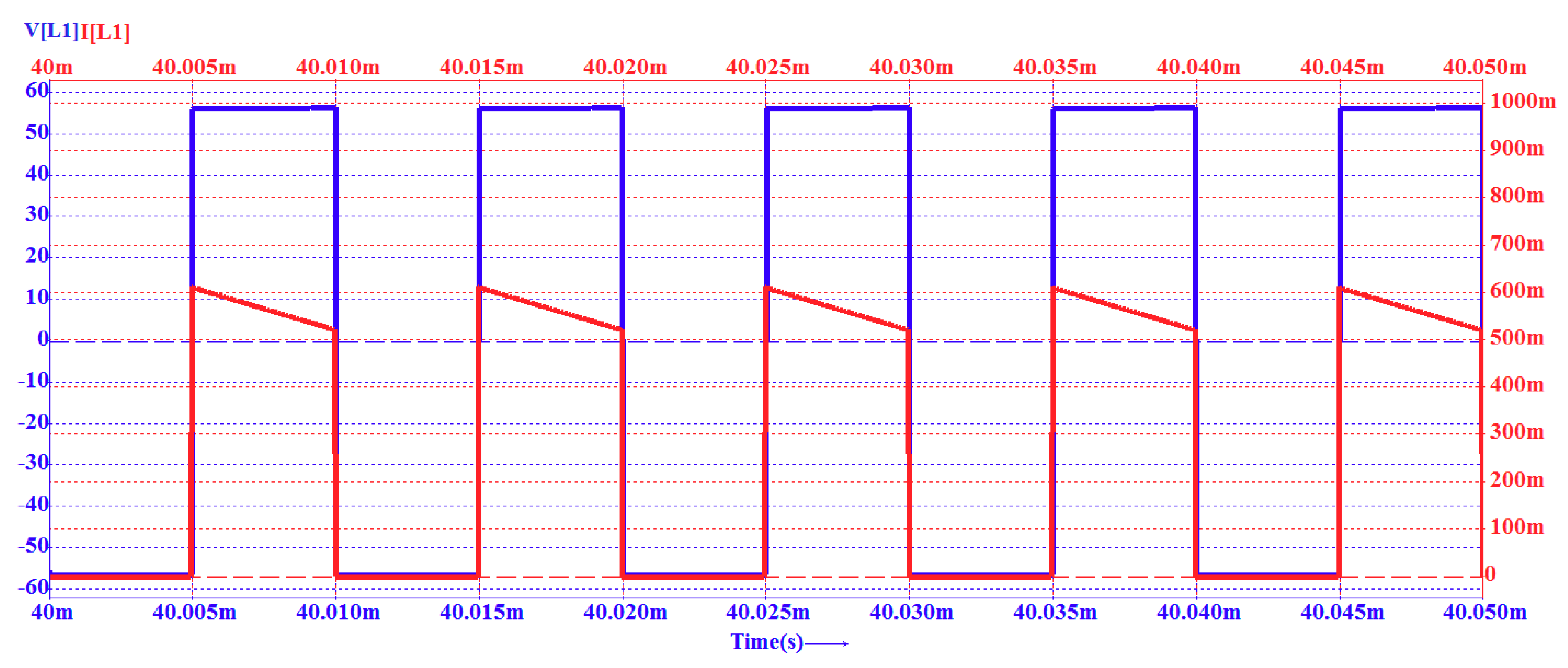
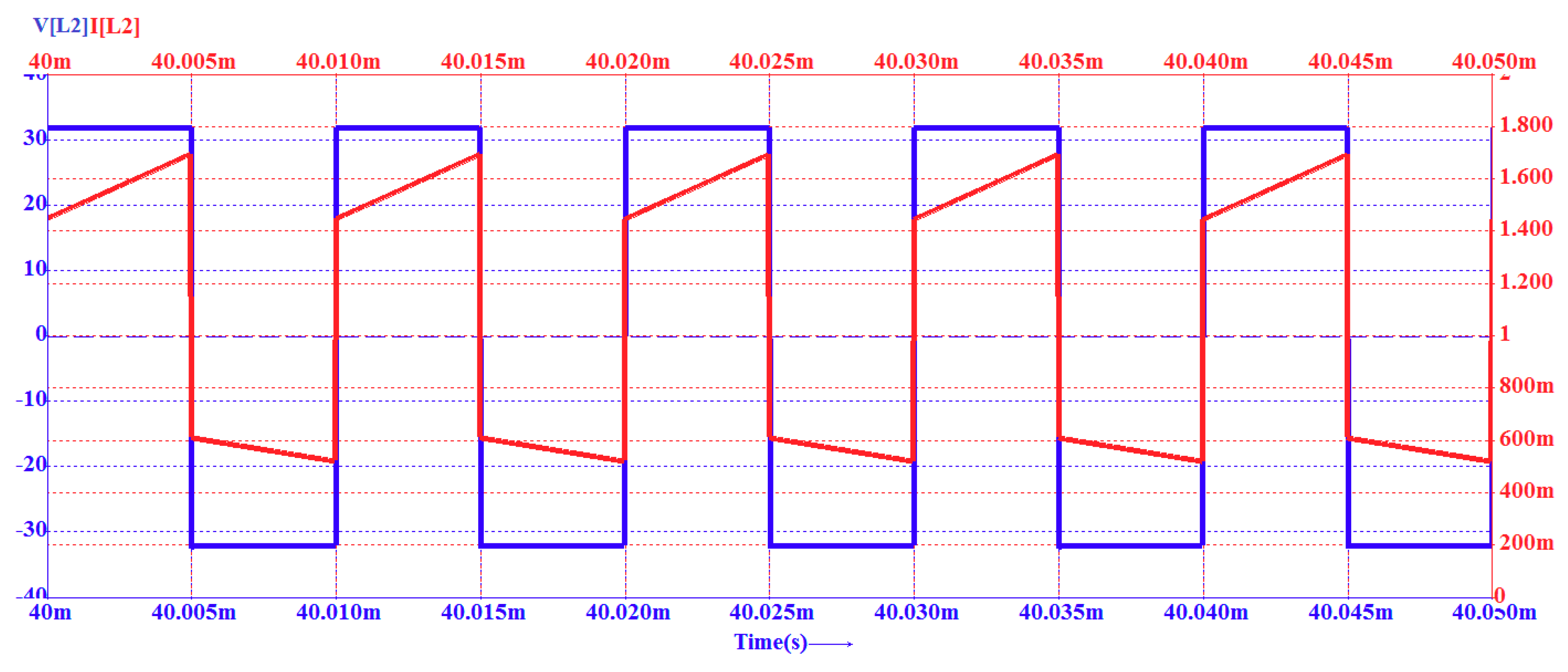
6. Simulation Results

To validate the theoretical considerations and correct operation in CCM for the ideal hybrid inductor-based Boost converter, a simulation in Caspoc software [55], was performed. All the devices were chosen ideal. The values of the components used in simulation were those resulted from the design:
Vg = 32 V, L1 = 2 mH, L2 = 644 μH, C = 12 µF, R = 432 Ω.
The PWM signal used for driving the gate of the transistor had the following parameters: fs = 100 kHz, D = 0.5. This results in a 120 V theoretical output voltage according to Equation (6). The dc output voltage—resulted from the simulation was 120 V indeed. In Figure 9, the input current ig can be seen. The voltage and current in the transformer primary winding are shown in Figure 10. Because of the coupled inductors, only a part of the triangular shape of the magnetizing current can be seen in the first inductor, while the other part of the triangular shape of the magnetizing inductor is located in the secondary, Figure 11. In Figure 12, the magnetizing current iLM can be seen being a triangular shape. The shape of the current together with the rectangular inductor voltage with two levels indicate that the converter operates correctly in CCM. Thus the correctness of the theoretical analysis is validated by the above CASPOC simulations.

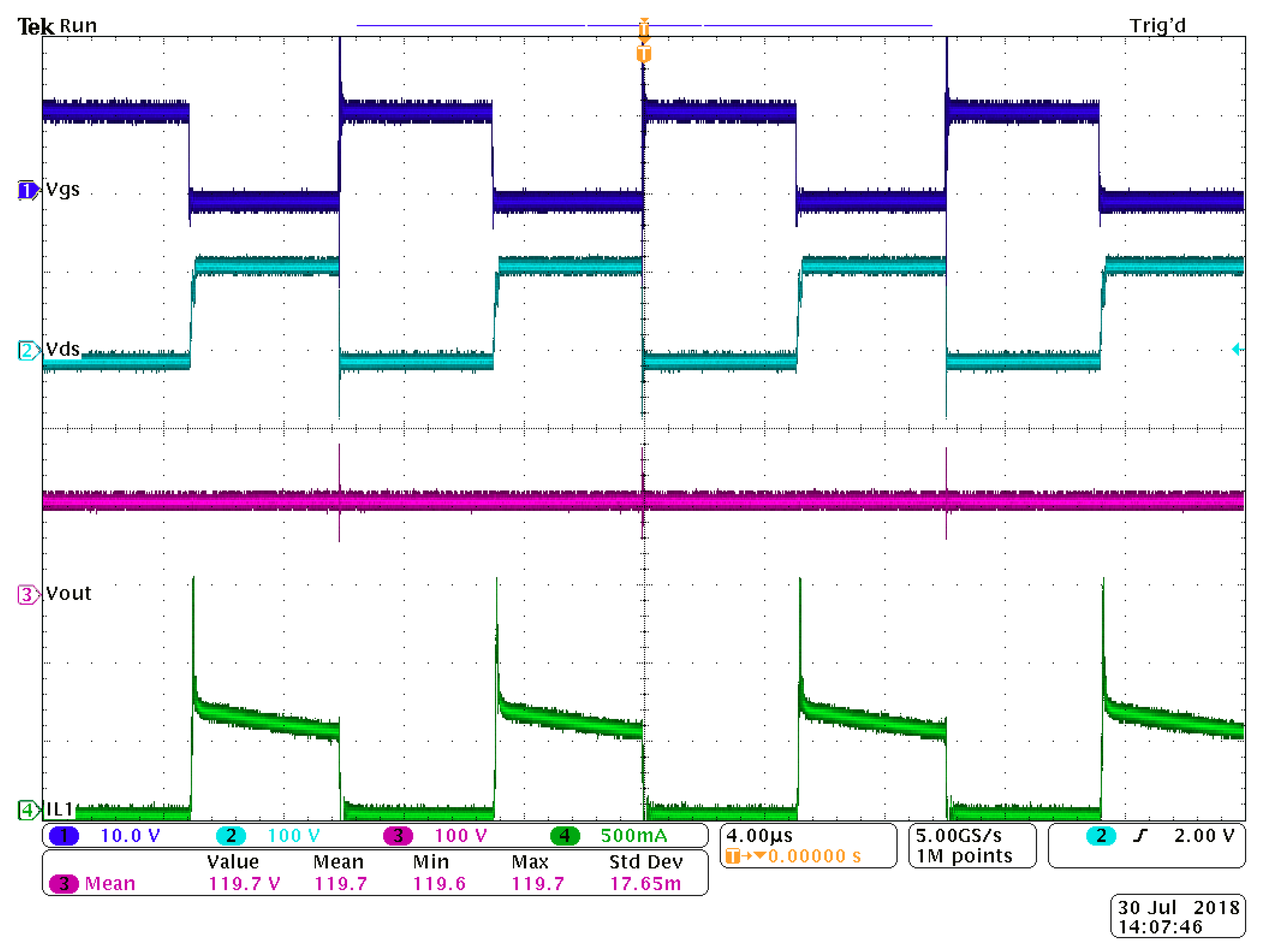
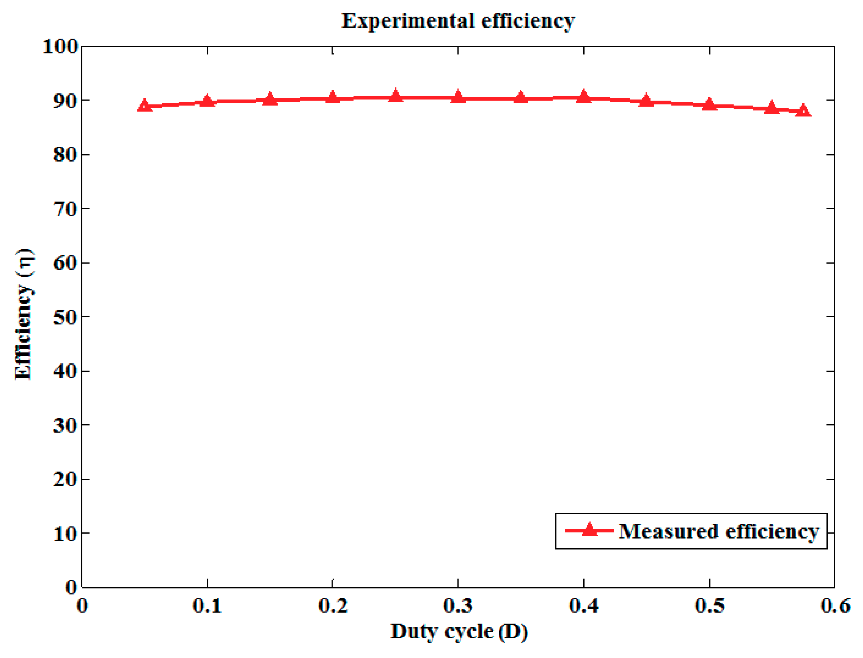
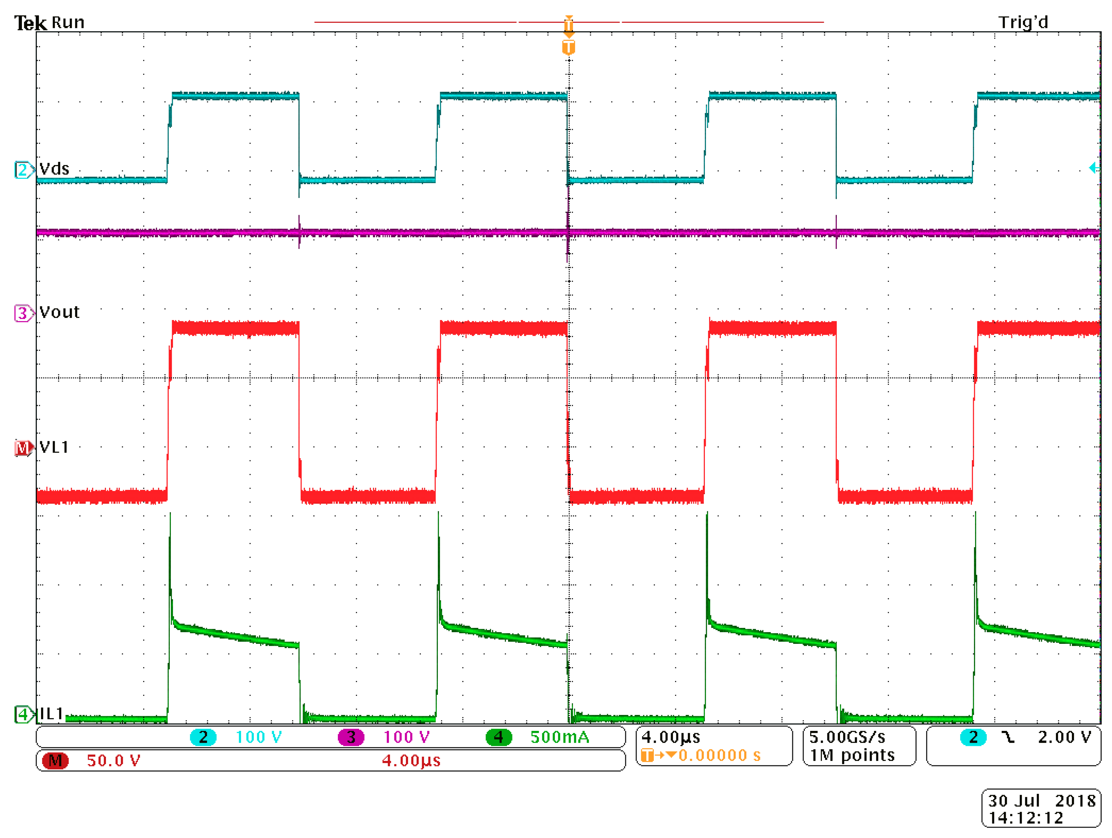
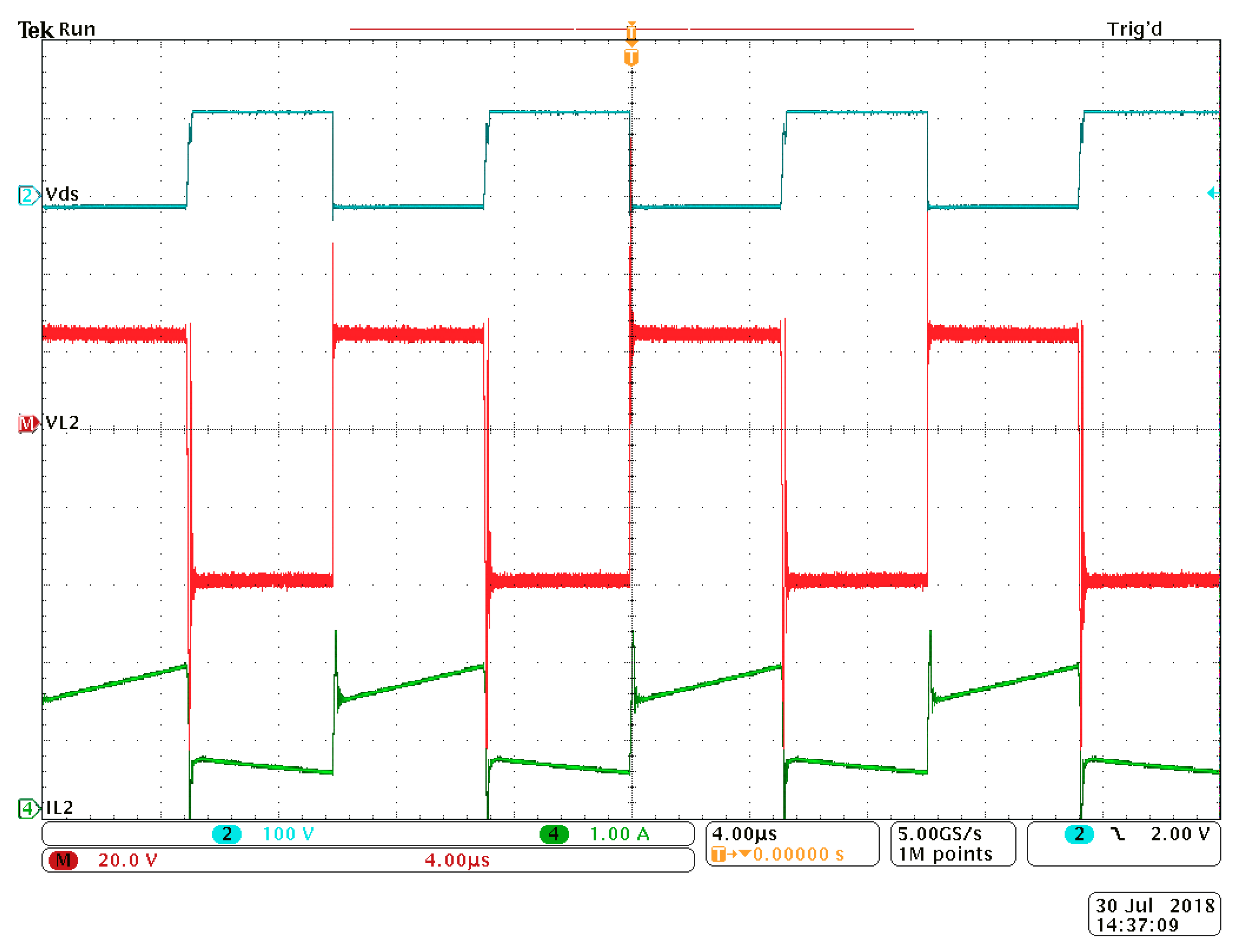
7. Experimental Results

In order to validate the functionality of the converter the measurements were performed first using a dc source instead of a PV panel. A test setup was configured, with a fixed input dc supply voltage Vg = 32 V and a fixed switching frequency fs = 100 kHz. The values for the inductors and capacitor are similar to the ones from the simulation. The semiconductors were: transistor S = Mosfet IPB073N15N5 (Infineon, El Segundo, CA, USA) and D2,3,4 = ROHM RFN10NS6SFH super fast recovery diodes. The MOSFET driver was the 1EDN7512BXTSA1 from Infineon. The acquired waveforms are depicted in Figure 13, Figure 14 and Figure 15.
In Figure 13 the following signals can be observed: the gate to source voltage with dark blue, the transistor drain to source voltage with cyan which is chosen as a reference signal and will be shown in all acquired waveforms, output voltage with magenta and the last one the current through L1 with green.
In Figure 14 the first waveform is the reference signal with cyan and the second waveform is the output voltage with magenta. The third signal depicted is the voltage across transformer primary winding (in red), exhibiting typical positive and negative constant levels and the last waveform is the current in the primary winding (shown in green).
The first waveform in Figure 15 is the transistor drain to source voltage that serves as a reference. The second and the third waveforms are the voltage measured on the secondary (with red), and the current in the secondary (drawn with green) respectively.
It may be observed that the waveforms are similar to the theoretical ones and the ones from simulation, both in qualitative and quantitative aspects. To draw the experimental static conversion ratio curve and calculate the efficiency of the converter the duty cycle of the transistor was modified. The input and output currents together with the output voltage were measured using the digital multimeter (DMM). The comparison for the dc conversion ratio between the experimental curve and the theoretical ideal curve is depicted in Figure 16, while in Figure 17 the computed results for the efficiency are synthetically presented. It can be remarked that the measured conversion ratio characteristic closely follows the ideal one and good efficiency, around 90%, is achieved.

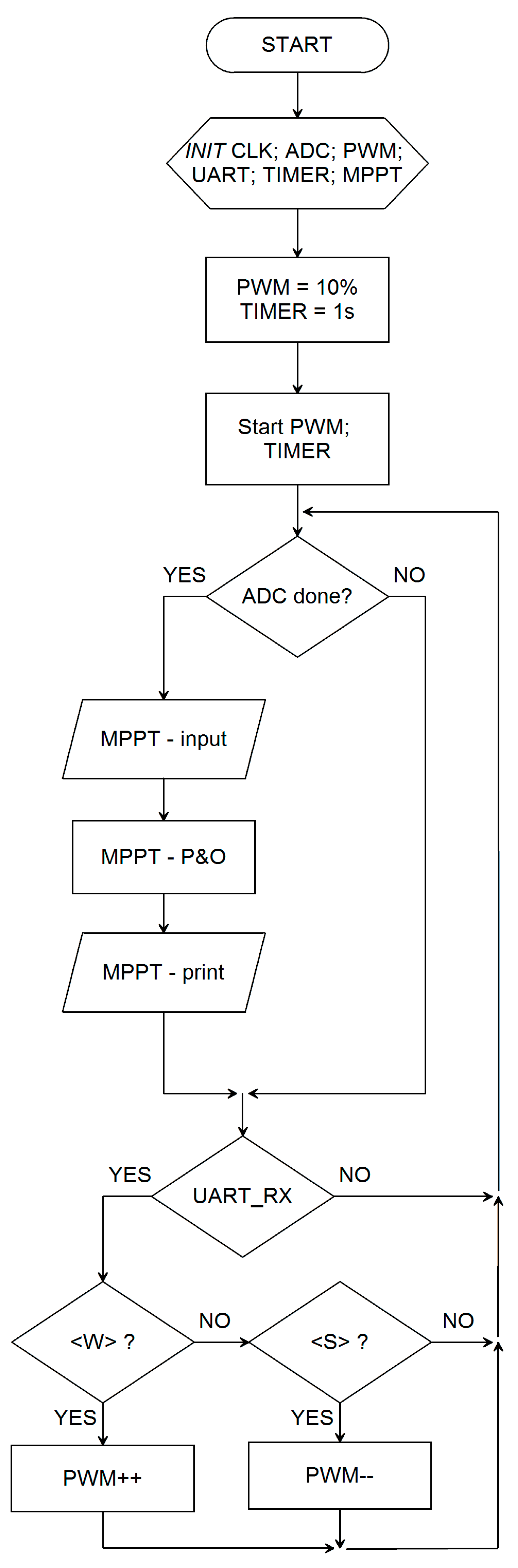
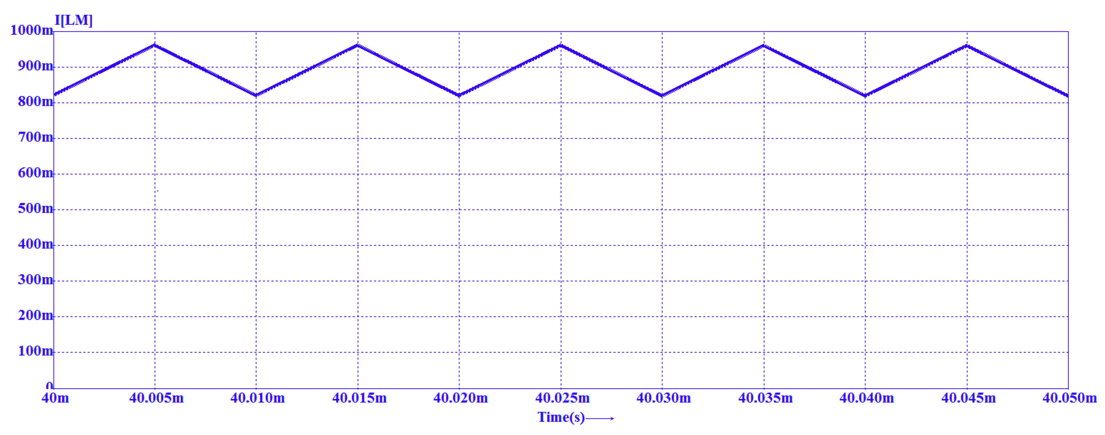
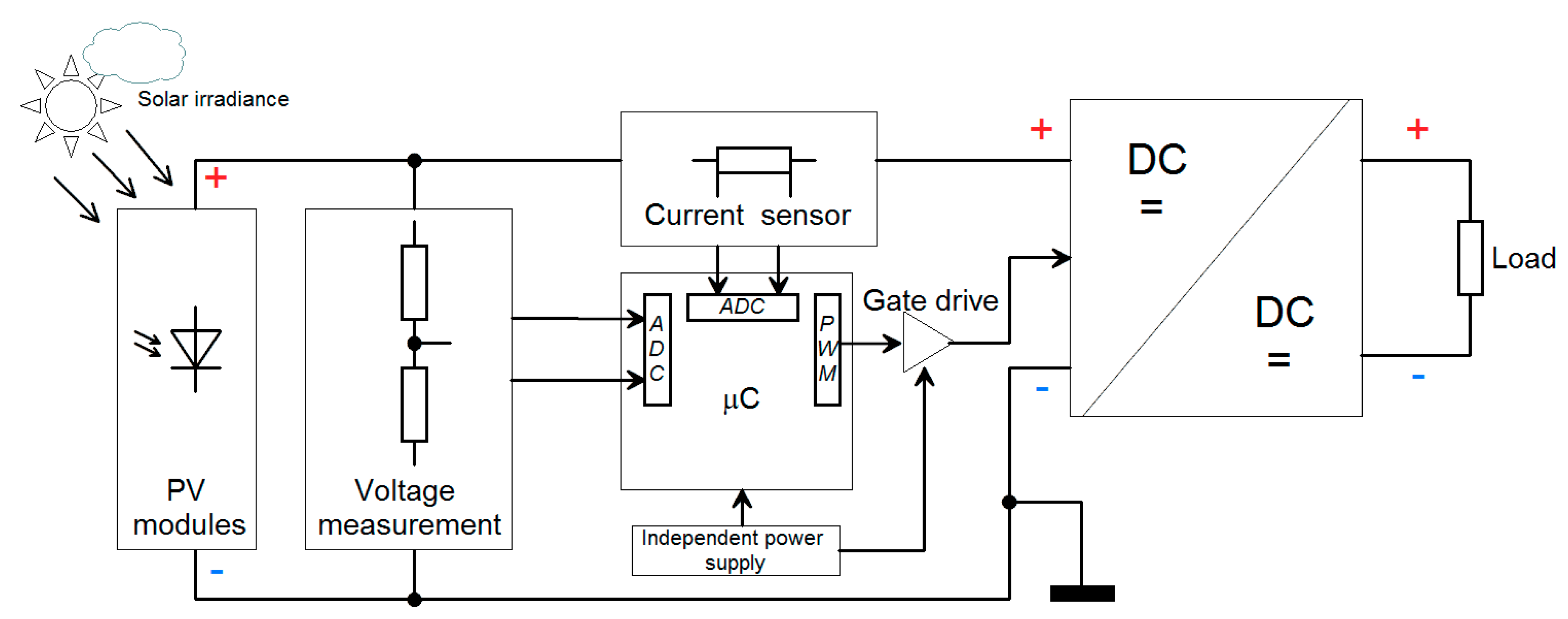
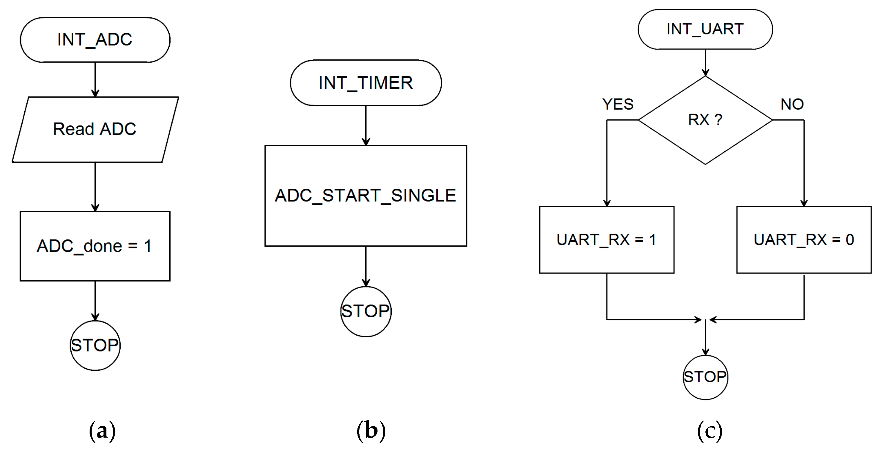
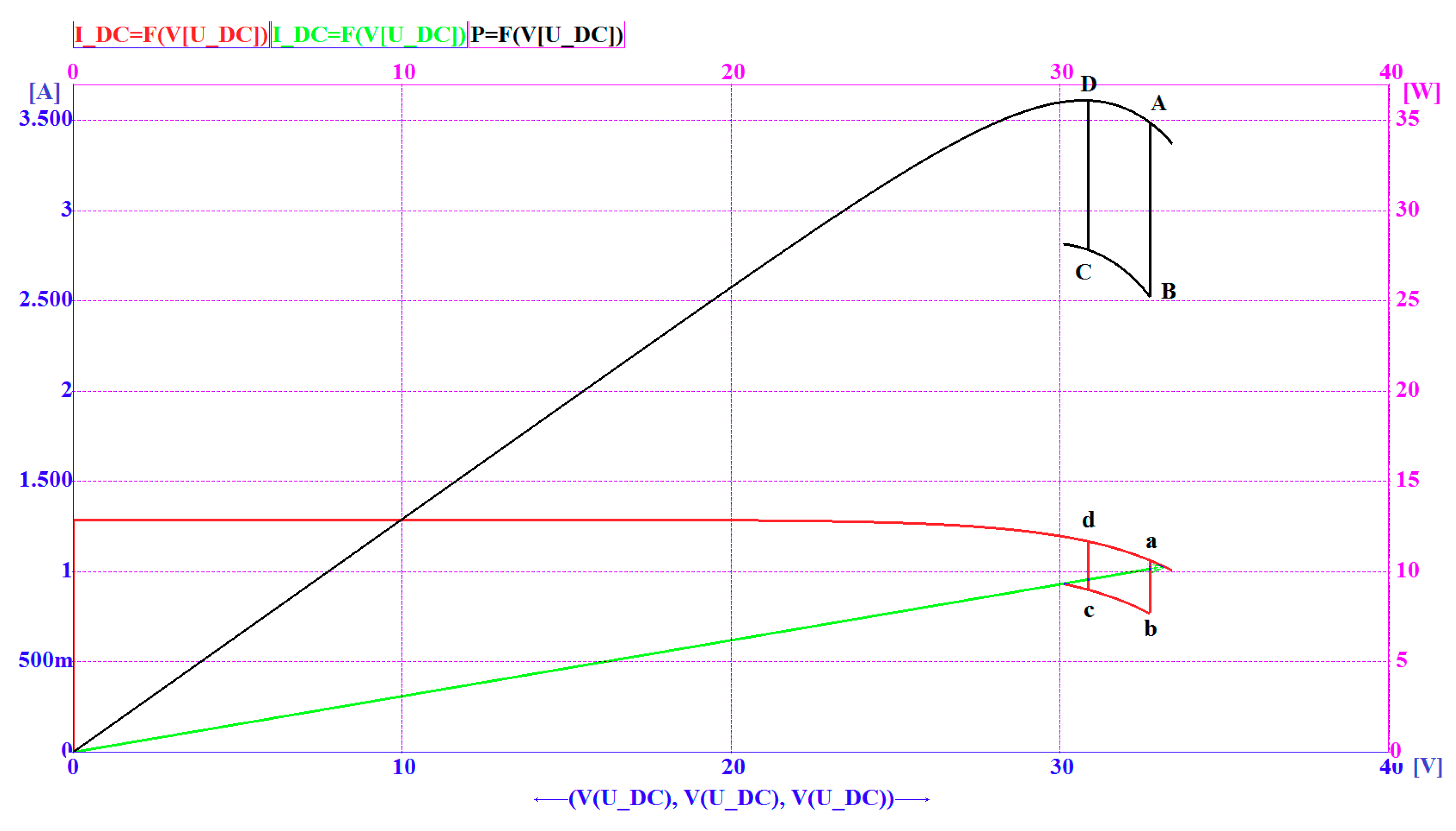
8. Application of the Proposed Converter in a PV System for Performing the MPPT

The block diagram of the PV system is presented in Figure 18.
For practically implementing the maximum power point (MPP) algorithm an ADuCino development board was chosen, equipped with the ADuCM360 ARM microcontroller (Analog Devices, Greater Boston, MA, USA) [56]. This features two independent analog to digital converter (ADC) delta-sigma channels, with 24 bits resolution. It can simultaneously sample and then it may perform multiple digital filtering. It also contains a programmable gain amplifier (PGA). This microcontroller was chosen to sample in the same time the current and the voltage provided by the PV modules. The current transducer was a LEM HO-8-NSM/SP33 with the three turns, having a nominal measurement current of 8/3 A [56]. The ADC was connected in a differential mode. The difference between the output voltage of the transducer Vout and the internal reference voltage Vref is acquired. The voltage across the PV modules is measured using a resistive divider that is also differentially connected to the ADC. Precision resistors with 0.1% tolerance were used.
The Cortex M3 core allows for calculations on 32 bits. The sensors and the gate-driver that were used are compatible with the 3V3 supply voltage of the microcontroller, thus avoiding the use of level-shifters. The flow chart of the software (Figure 19) starts with the initialization of the clock system alongside with the necessary modules: ADC, PWM, Universal Asynchronous Receiver Transmitter (UART), TIMER and of the MPPT algorithm.
The PWM is stated at an initial duty cycle of 10% and the TIMER is set to interrupt at a rate of 1 s, waiting for the result of the ADC conversion. The MPPT algorithm implements the P&O strategy [57,58,59,60,61,62,63,64,65] according to subroutine flowchart revealed in Figure 20. For laboratory testing it was overseen the feature to interact with the software through the UART port in order to manually modify the increase or decrease of the duty cycle through two commands. When character <W> is received then the duty cycle will be increased while when character <S> is received it will be decreased. If nothing is received the MPPT algorithm runs freely. The TIMER interrupt, Figure 20b, is triggered each 1 s and starts a single simultaneous ADC conversion for both channels. In Figure 20c it is depicted the UART interrupt at receiving. This sets the UART_RX flag if a character was received. The decision based on the received character is implemented in the main loop.
The MPPT algorithm with P&O is detailed in Figure 21.
Initially the increment (INC) direction is declared. Then the power Pk is calculated based on the actual voltage and current values acquired. Then the algorithm will compare this value to the power Pk−1 calculated at the previous step. If Pk > Pk−1 then the duty cycle of the PWM signal will be incremented. Then the power Pk−1 will be retested at the next pass through the algorithm branch. While the power increases, the duty cycle will be increased step by step. In the moment when the maximum power point has been overtaken, Pk < Pk−1, and the direction will be changed to decrement (DEC), while the duty cycle will be diminished. When the MPP is overtaken in the opposite direction and Pk < Pk−1 again the direction will be changed from DEC to INC and the algorithm continues this way. The minimum and maximum values of the duty cycle than cannot be exceeded are set as constants during the software initialization.

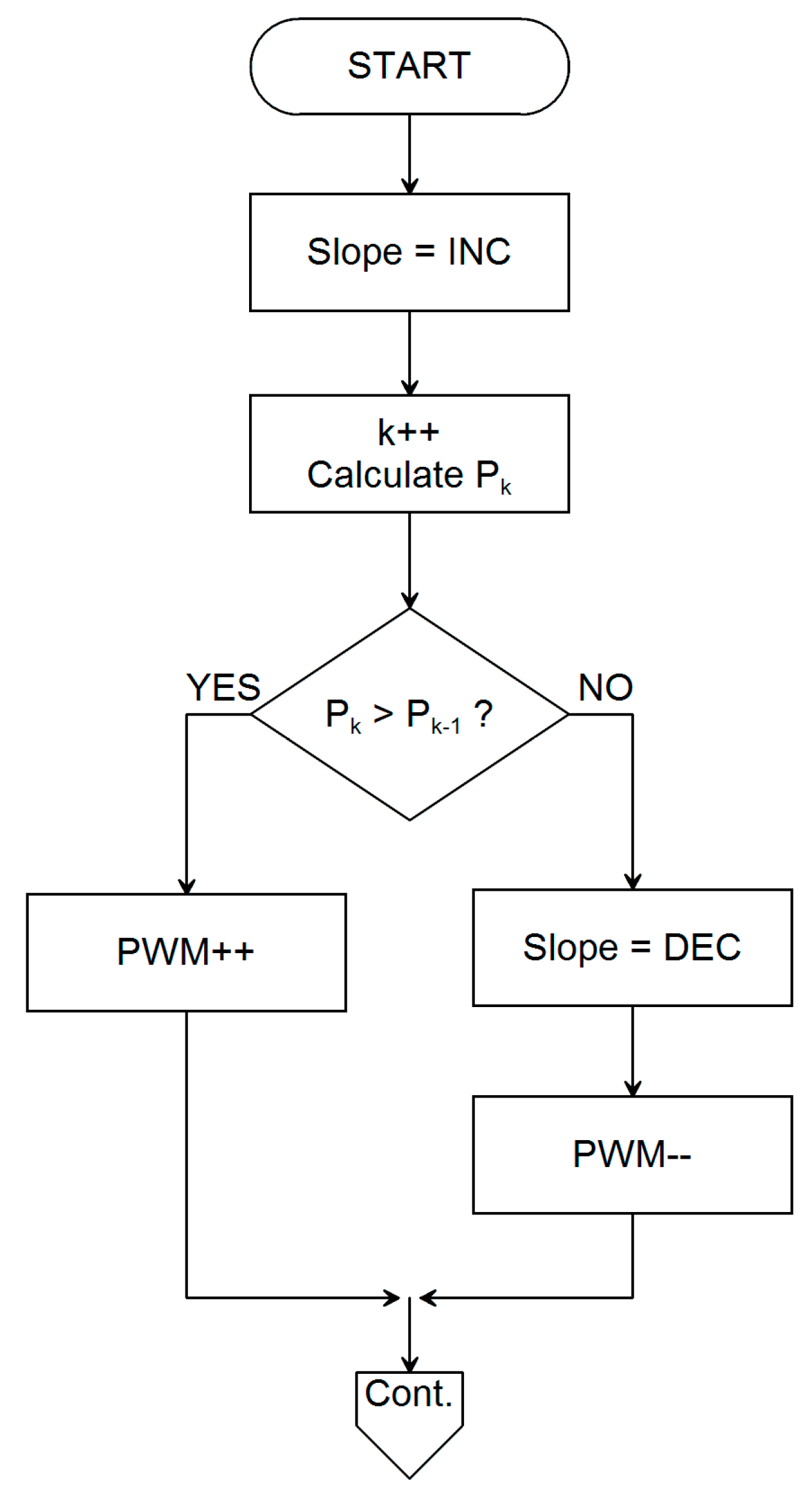
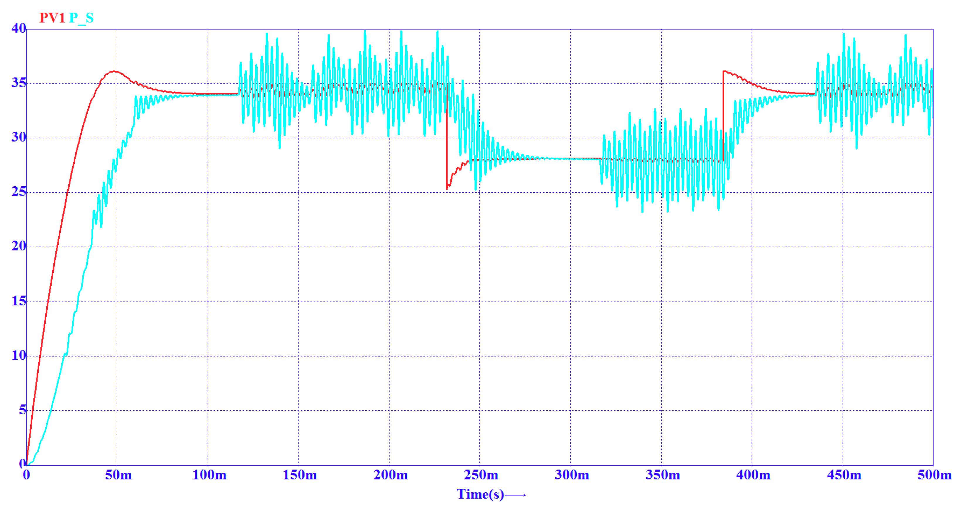
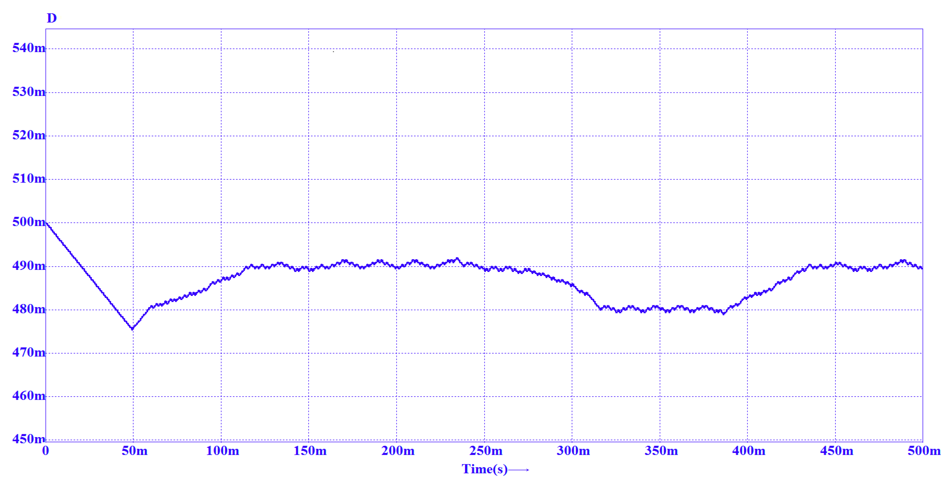
8.1. Simulation of the MPPT Algorithm Using the Proposed Hybrid Inductor-Based Boost Converter in a PV System

Simulations using CASPOC were performed for tracing the PV modules characteristic curves and the results are depicted in Figure 22. The obtained results are for a temperature of Ta = 60 °C and an incident irradiance G1,2,3 equaling 600, 800 and 1000 W/m2. With (0) are marked the results for an irradiance of 600 W/m2, with (1) for an irradiance of 800 W/m2 and with (2) for an irradiance of 1000 W/m2.
At an irradiance of 1000 W/m2 the maximum power obtained was 36.16 W, at a voltage of V = 30.73 V and a current I = 1.17 A. The short circuit current was Isc = 1.292 A and open circuit voltage was Voc = 38.02 V. For an irradiance of 800 W/m2, the maximum power obtained was 28.25 W, corresponding to a voltage of 29.60 V and a current I = 0.95 A, short circuit current Isc = 1.048 A and an open circuit voltage Voc = 36.62 V. From the last measurement, at an irradiance of 600 W/m2, the maximum power is 20.61 W at a voltage of V = 28.15 V and a current of I = 0.73 A. The short circuit current was Isc = 0.804 A and the open circuit voltage was Voc = 34.82 V.
A simulation using the proposed hybrid step-up converter with the same values for the components as the ones from the previous chapter and using PV panels with the same characteristics like the ones used in the practical circuit were performed. In Figure 23, on the input-output power characteristic until about 100 ms there is a transient start-up mode, after which, at time T1 = 233 ms, a step change from G3 = 1000 W/m2 to G2 = 800 W/m2 in solar irradiance occurs. After reaching the new steady state, at time T2 = 385 ms, a new step increase in the irradiance from G2 = 800 W/m2 back to G3 = 1000 W/m2 takes place. The MPPT control loop regulates the absorbed power from the panel to about 34.5 W at an irradiance equals to 1000 W/m2.
On the characteristic in Figure 24 it can be seen that at the end of simulation the arrow is beyond the maximum power point due to the P&O control strategy. The green arrow shows the instantaneous position of the operating point on the current-voltage characteristic during the simulation, being able to follow the transition on the characteristic before and after the maximum point. The duty cycle that results from the P&O algorithm is depicted in Figure 25. As before, the steady state operation is achieved after 100 ms. The duty cycle is slightly modified around the value of 49%. Figure 26 shows that the desired average voltage of 120 V can be achieved. The simulation time was 500 ms, out of which the first 100 ms is a transient mode. The simulation step was 100 ns and then the results were displayed every five samples.
At the start of the simulation all voltages and currents are considered to be zero. Initially, the input capacitor is placed across the terminals of the PV module at the input of the hybrid Boost converter, is uncharged. As a result, this input capacitor will force the PV module to operate at short-circuit current for a short period of time. As simulation time passes, the capacitor will accumulate charge and the voltage across the PV module will consequently increase. The operation point will move towards the MPP and in approximatively 80 ms the operating point will achieve VPV = 34 V. Then the new hybrid inductor-based Boost converter becomes operational and the MPPT algorithm searches to adjust the operating point of the PV module to the maximum power harvested. The voltage at the output of the converter starts to be quasi-stable if the irradiance or the load do not modify. Practically, the system has come to equilibrium being in steady-state after approximately 100 ms from start. At the time T1 = 233 ms a step transition from G3 = 1000 W/m2 to G2 = 800 W/m2 in solar irradiance was simulated. On the power characteristic, an instantaneous displacement is produced from points A to B and on the current-voltage curve and the operating point moves from a to b. Because the load resistance is unmodified, the controller will move the operating point from B to C and from b to c, respectively. This adaptation is due the decrease of the input power. At time T2 = 385 ms a step increase in the irradiance from G2 = 800 W/m2 to G3 = 1000 W/m2 was simulated. As a result, the transitions on characteristics will be from C to D and from c to d respectively. Again, the algorithm will search for the MPP and will act in order to maximize the power. At the final of the simulation, at T3 = 500 ms, the operating point will be placed on the current characteristic with the green arrow, which also indicates the instantaneous operating point on current-voltage characteristic curve during the simulation. The output voltage is constant and equal to 120 V until irradiance is decreasing, when the output voltage is regulated to a voltage equal to 110 V, and is equal again to 120 V if the irradiance is increasing. Figure 25 shows the variation of the duty cycle represented in the time domain, but only one from five measurements is shown. From these figures it can be seen the correlation between power characteristic, voltage characteristic and duty cycle.

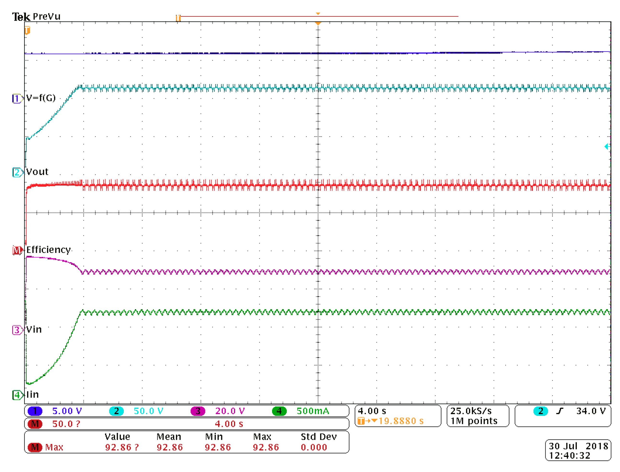
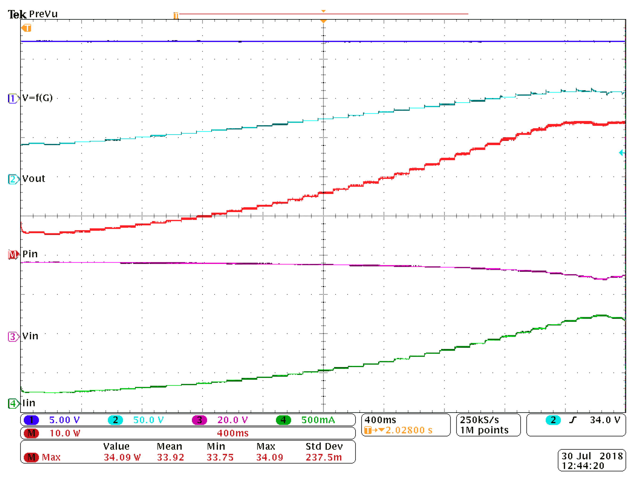
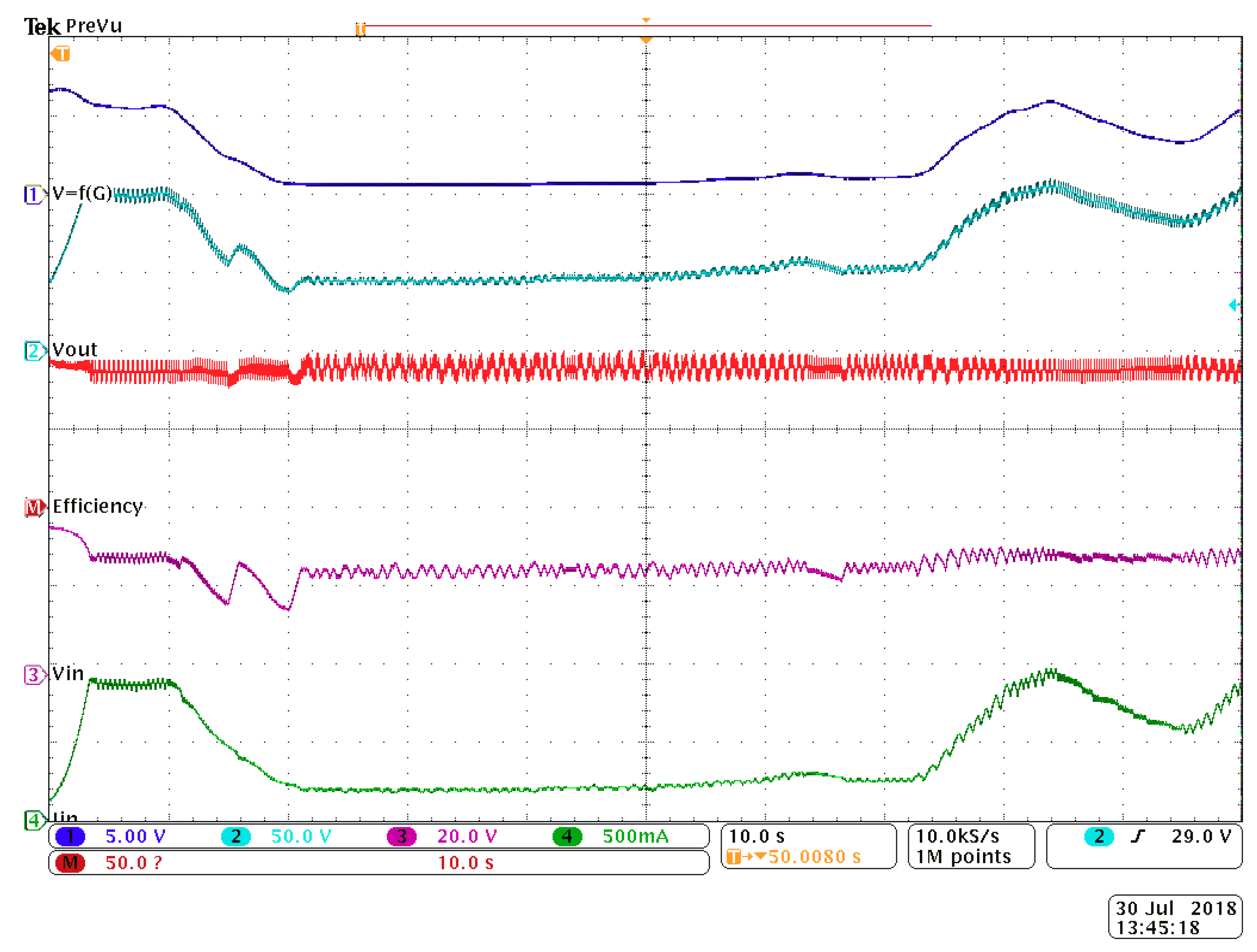
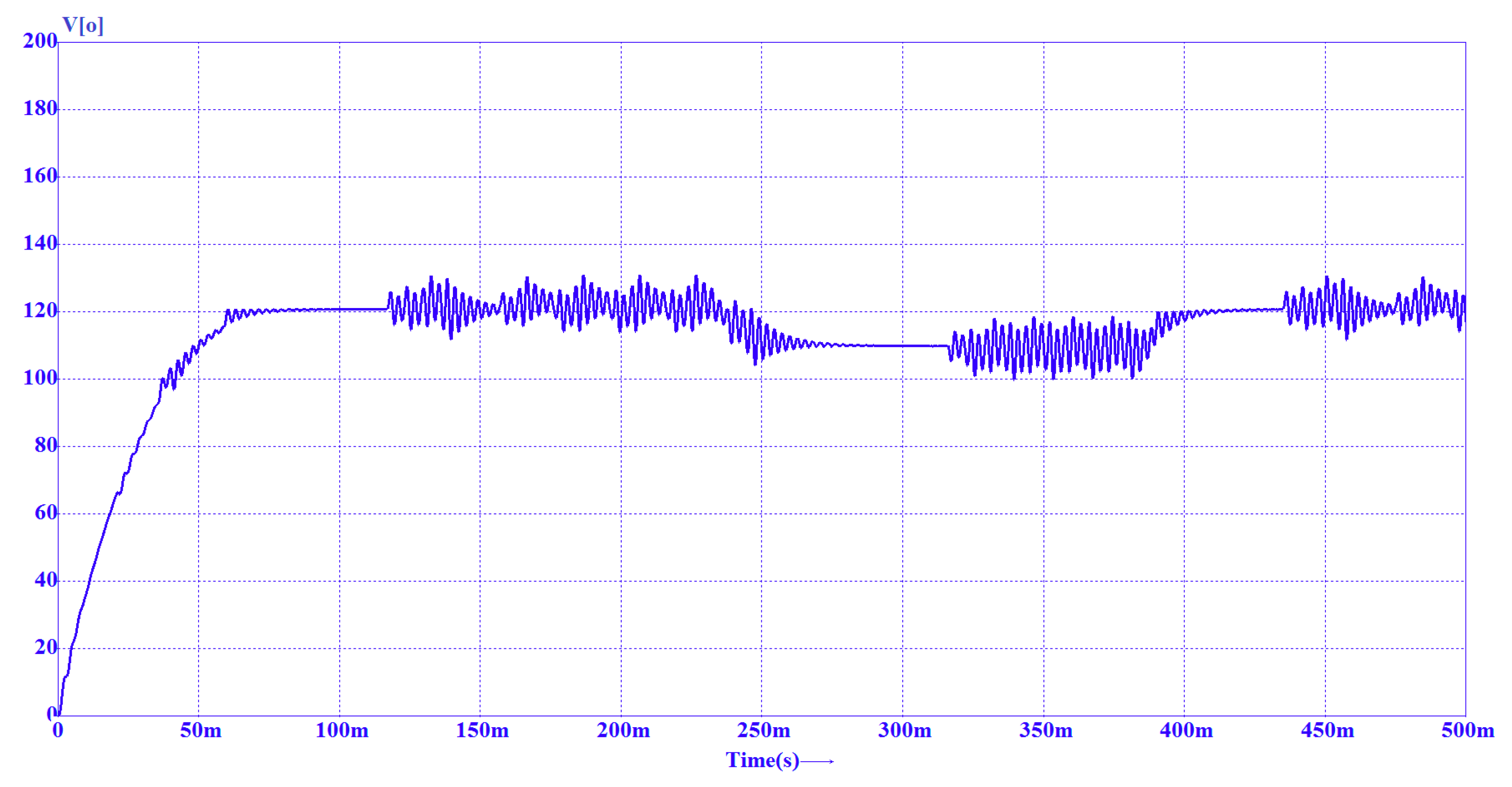
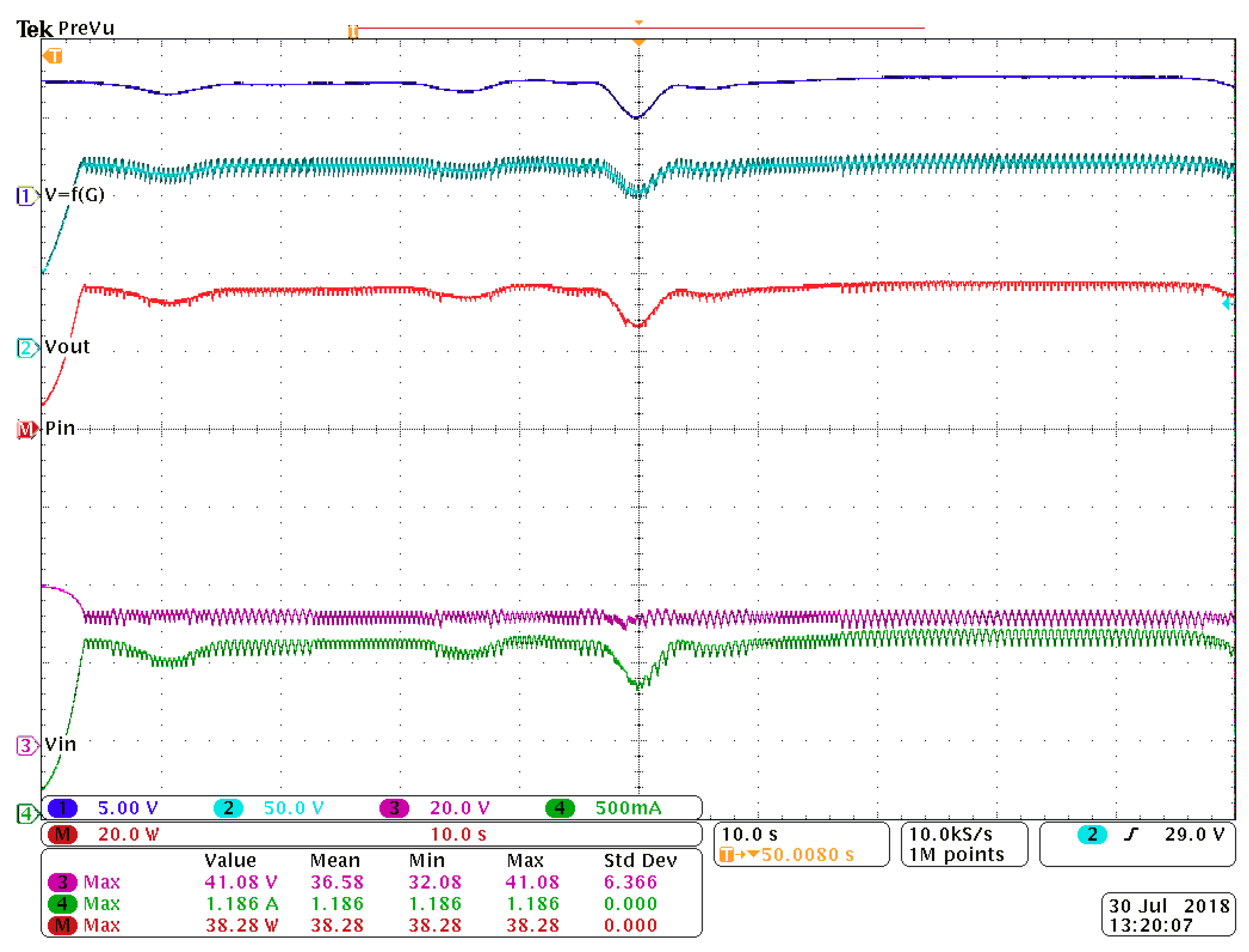
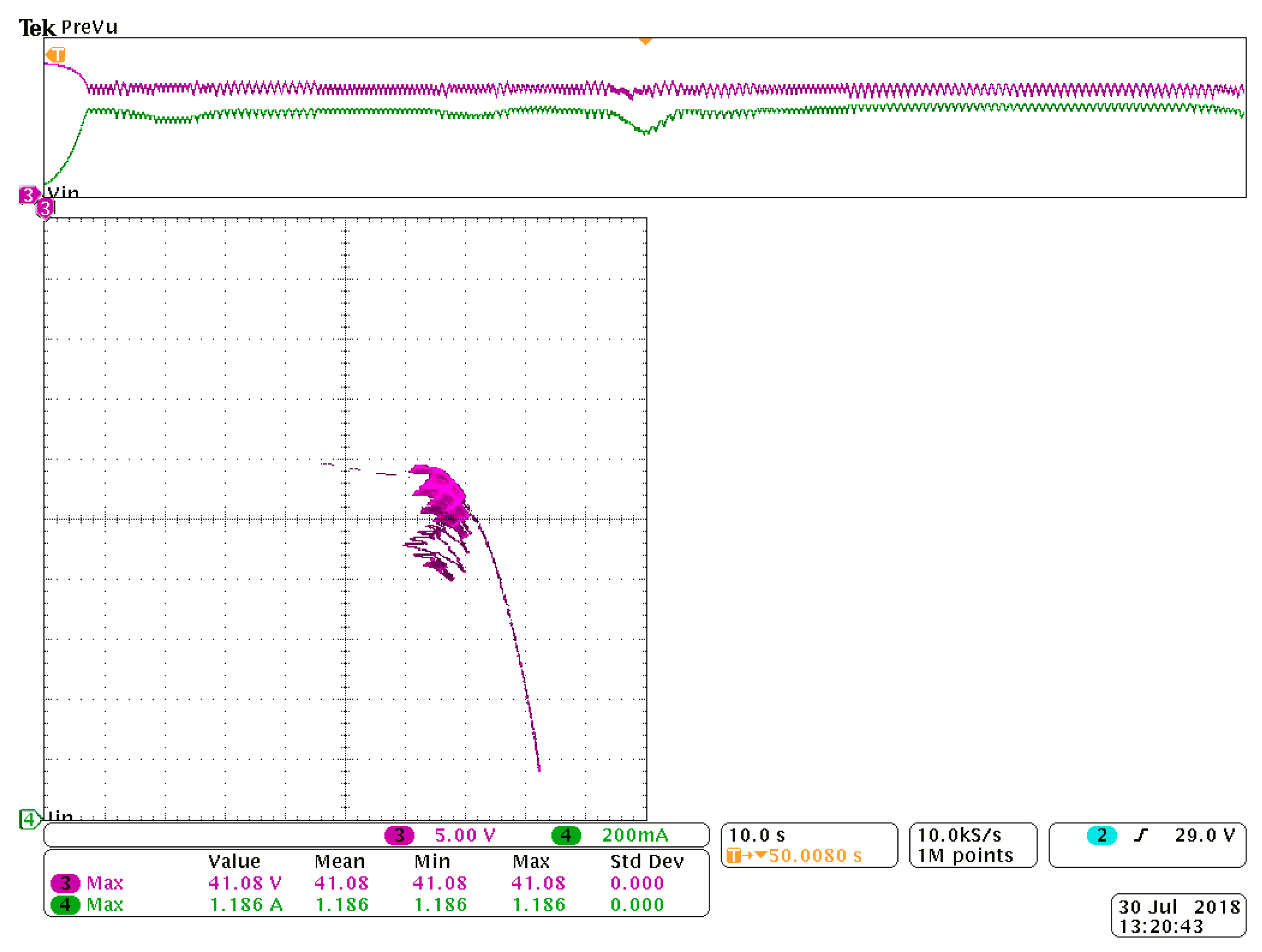
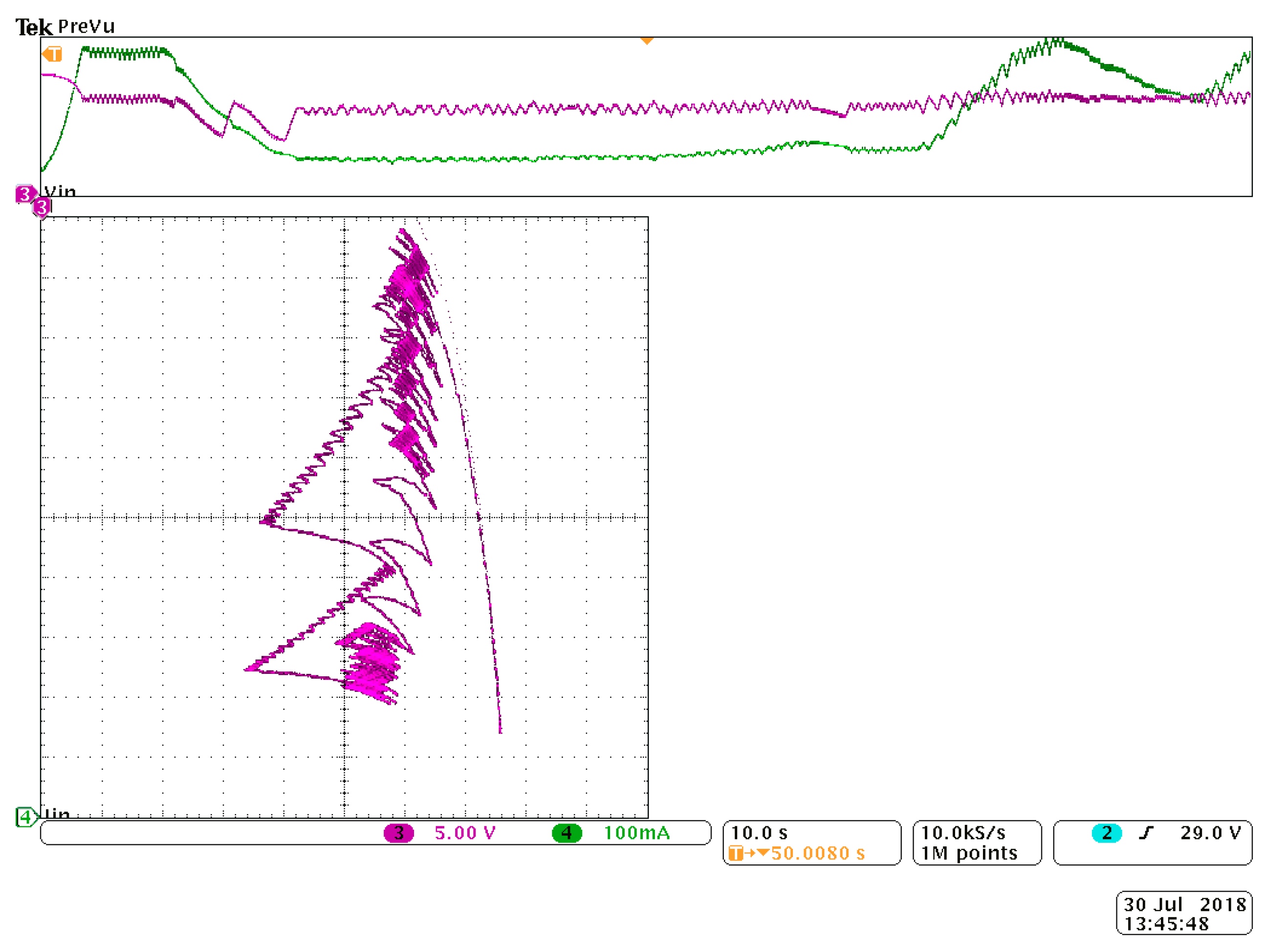
8.2. Practical Results of the MPPT Algorithm Using the Proposed Hybrid Inductor-Based Boost Converter

For functional testing of the new proposed converter supplied by PV panels and employing a MPPT controller, some measurements under constant irradiance coming from the Sun and clear sky conditions were acquired. A pyranometer that produces a voltage proportional to the incident solar irradiance was used. In the experiment in Figure 27 the voltage provided by the solar sensor, depicted with dark blue and labeled “V = f(G)”, was constant and approximately 6 V, corresponding to an irradiance of 720 W/m2. The oscilloscope capture shows the start-up, which lasts approximately 4 s and then the steady state is achieved. This is clearly visible in the waveforms which are explained below. In the second waveform depicted with cyan and labeled “Vout” it is remarked that when the MPP is reached, the voltage stays at a constant value. The P&O algorithm continuously modifies the duty cycle by incrementing and decrementing it with one step, and in our case, when the irradiance is constant, it maintains the converter around the same operating point. The third waveform, depicted with red and labeled “Efficiency”, is the instantaneous efficiency of the converter. It was computed based on the assumption that a constant load resistance was used. It may be remarked that the converter achieves good and steady efficiency even during startup. Small steps are also remarked because of the P&O MPPT. The fourth waveform is the input voltage, drawn with magenta and labeled “Vin”. It may be seen that Vin starts from the open-circuit voltage of about 36 V and decreases according to the characteristic curve of a PV cell until the MPP is reached.
The fifth signal, labeled “Iin, green colored, is the input current absorbed by the converter from the PV modules. It increases until the steady state of about 1.1 A is achieved. Also the steps of the control algorithm are visible. The last-mentioned input measurements are used by the microcontroller to drive the converter such that the product of them, the harvested power, to be maintained maximal.
Figure 28 shows another oscilloscope capture with the start of the system assuming constant solar irradiance conditions in order to see much clearer the steps performed by the MPPT algorithm and observe if it operates correctly, without any overshoot. It can be obviously remarked that the duty cycle is updated each 100 ms, modifying the operating point of the converter. The first waveform, drawn with dark blue and labeled “V = f(G)”, is the voltage from the pyranometric sensor. It is constant at about 7.1 V, corresponding to a solar incident irradiance of 852 W/m2. The second signal, with cyan and with the label “Vout”, is the output voltage of the converter, which will rise to more than 100 V. The third signal, represented with red and labeled “Pin”, is the instantaneous power at the input, provided by the PV cell and that needs to be maximized by the control algorithm. It is computed by performing the product of the voltage and current at the input.
The maximum harvested power in the stated conditions was about 34 W. The third waveform is drawn with magenta and labeled “Vin”. At the beginning it is equal to the open-circuit voltage of the PV panels, of about 34 V and then decreases according to characteristic to about 28 V. The fifth signal is the input current, with the label “Iin” and depicted with green. It increases to 1.1 A as MPP is reached. As current increases and input voltage slightly decreases, the input power provided by solar conversion increases. This proves the correct behavior of the control algorithm.
In Figure 29 the same waveforms as in Figure 28 are depicted, but in this case a small and transparent cloud passes through, causing some small decreases in the irradiance. The signals are the same as the previous ones. The steps of the P&O implementation are visible and it is remarked that the power is related to the irradiance. At about 50 s the biggest decrease can be observed, because that time the densest part of the cloud occurs.
The converter input measurements from Figure 29 are represented using the XoY chart in Figure 30. The thickened part of the characteristic is the zone of MPP on the average irradiance characteristic. The small decrease is caused by the dense part of the cloud. Then, when the irradiance changes, the algorithm maintains the operating point around the line that contains the MPPs for different irradiance values. Practically it goes from a characteristic curve to another, being known that these curves depend on the incident irradiance. The conclusion is that the implemented controller is capable to maintain the operation around the MPP as the atmospheric conditions change.
Figure 31 shows the behavior when a small but dense cloud crosses in front of the Sun. The acquired waveforms are the same to those in Figure 27. The decrease of the global irradiance depicted by the first blue signal is abrupt, reaching about 100 W/m2 at the minimum. In the third red waveform the instantaneous efficiency is represented. It is remarked that there is no change in the efficiency when the atmospheric conditions modify. It is important to have a high efficiency when there is less sunlight and the harvested power is reduced.
The input signals from Figure 31 are represented in XoY axes in Figure 32. Because of the long standing at different incident irradiances there are many characteristic curves on which the controller must search the MPP. That is why there are many thickened regions. But, most important, it may be remarked that the operating point is maintained on the line of MPPs, proving the correct operation of the implemented controller again. Hence the switching frequency, the sampling rate, the computation speed and the update rate were correctly chosen for the digital controller, proving the right design. The proposed system based on the proposed converter is thus a good solution for solar energy harvesting.

9. Conclusions

A new hybrid inductor-based Boost topology for DC-DC conversion is presented. In spite of its simplicity, the converter has several desirable features: it is still a second order converter that makes controller design similar to that of a classical Boost topology. Moreover, compared to other topologies with a step-up characteristic it exhibits lower current and voltage stresses for the same conversion conditions. All the relationships needed for the design are provided and the converter operation was verified through simulation and experiments. The measurements performed showed an excellent efficiency and they all confirmed and validated the theoretical considerations. Finally, it was demonstrated how this converter can be integrated in a PV system in order to perform the MPP operation. The experimental results proved the suitability of the new topology in solar energy systems.

Author Contributions

All authors contributed to this research. I.-M.P.-C. and S.L. conceived and designed the study. I.L. and R.M. developed the MATLAB programs for analyzing the lossy converter and the corresponding data from experiments. S.P. and D.L. performed the Caspoc simulations for the new proposed inductor-based Boost converter. S.P. and R.M. performed the Caspoc simulations for the MPPT algorithm. S.P., D.L. and I.L. wrote the software algorithm for the MPPT. S.L., S.P. and I.-M.P.-C. handled the experiments. I.-M.P.-C. wrote the paper and managed all the correspondence with the editor. D.L. reviewed the manuscript. All authors read and approved the final manuscript.

Funding

This work was partially supported by research grant PCD-TC-2017 and Politehnica University Timisoara.

Conflicts of Interest

The authors declare no conflict of interest.

References

  1. Coyle, E.D.; Simmons, R.A. Understanding the Global Energy Crisis; Purdue University Press: West Lafayette, IN, USA, 2014; pp. 1–301. [Google Scholar]
  2. Abolhosseini, S.; Heshmati, A.; Altmann, J. A review of renewable energy supply and energy efficiency technologies. IZA Discuss. Pap. Ser. 2014, 8145, 1–35. [Google Scholar]
  3. Report of REN21 Renewable Energy Policy Network for the 21st Century—10 Years of Renewable Energy Progress; Renewable Energy Policy Network for the 21st Century, REN21 Secretariat: Paris, France, 2014; pp. 1–48. Available online: http://www.ren21.net/spotlight/10-years-report/ (accessed on 16 December 2018).
  4. Pali, B.S.; Vadhera, S. Renewable Energy Systems for Generating Electric Power: A Review. In Proceedings of the 2016 IEEE 1st International Conference on Power Electronics, Intelligent Control and Energy Systems (ICPEICES), Delhi, India, 4–6 July 2016; pp. 1–6. [Google Scholar]
  5. Nehrir, M.H.; Wang, C.; Strunz, K.; Aki, H.; Ramakumar, R.; Bing, J.; Miao, Z.; Salameh, Z. A review of hybrid renewable/alternative energy systems for electric power generation: Configurations, control, and applications. IEEE Trans. Sustain. Energy 2011, 2, 392–403. [Google Scholar] [CrossRef]
  6. Jin, C.; Sheng, X.; Ghosh, P. Optimized electric vehicle charging with intermittent renewable energy sources. IEEE J. Sel. Top. Signal Process. 2014, 8, 1063–1072. [Google Scholar] [CrossRef]
  7. Sun, J.; Li, M.; Zhang, Z.; Xu, T.; He, J.; Wang, H.; Li, G. Renewable energy transmission by HVDC across the continent: System challenges and opportunities. CSEE J. Power Energy Syst. 2017, 3, 353–364. [Google Scholar] [CrossRef]
  8. Zhang, T.; Chen, W.; Han, Z.; Cao, Z. Charging scheduling of electric vehicles with local renewable energy under uncertain electric vehicle arrival and grid power price. IEEE Trans. Veh. Technol. 2014, 63, 2600–2612. [Google Scholar] [CrossRef]
  9. Dai, J.; Dong, M.; Ye, R.; Ma, A.; Yang, W. A Review on Electric Vehicles and Renewable Energy Synergies in Smart Grid. In Proceedings of the 2016 China International Conference on Electricity Distribution (CICED), Xi’an, China, 10–13 August 2016; pp. 1–4. [Google Scholar]
  10. Umuhoza, J.; Zhang, Y.; Zhao, S.; Mantooth, H.A. An Adaptive Control Strategy for Power Balance and the Intermittency Mitigation in Battery-PV Energy System at Residential DC Microgrid Level. In Proceedings of the 2017 IEEE Applied Power Electronics Conference and Exposition (APEC), Tampa, FL, USA, 26–30 March 2017; pp. 1341–1345. [Google Scholar]
  11. Basaran, K.; Cetin, N.S.; Borekci, S. Energy management for on-grid and off-grid wind/PV and battery hybrid systems. IET Renew. Power Gener. 2017, 11, 642–649. [Google Scholar] [CrossRef]
  12. Paredes-Parra, J.M.; Mateo-Aroca, A.; Silvente-Niñirola, G.; Bueso, M.C.; Molina-García, Á. PV module monitoring system based on low-cost solutions: Wireless Raspberry application and assessment. Energies 2018, 11, 3051. [Google Scholar] [CrossRef]
  13. Caruso, M.; Di Tommaso, A.O.; Imburgia, A.; Longo, M.; Miceli, R.; Romano, P.; Salvo, G.; Schettino, G.; Spataro, C.; Viola, F. Economic Evaluation of PV System for EV Charging Stations: Comparison between matching Maximum Orientation and Storage System Employment. In Proceedings of the 5th International Conference on Renewable Energy Research and Applications (ICRERA), Birmingham, UK, 20–23 November 2016; pp. 1179–1184. [Google Scholar]
  14. Chaudhari, K.; Ukil, A.; Kumar, K.N.; Manandhar, U.; Kollimalla, S.K. Hybrid optimization for economic deployment of ESS in PV-integrated EV charging stations. IEEE Trans. Ind. Inf. 2018, 14, 106–116. [Google Scholar] [CrossRef]
  15. Sreedevi, J.; Ashwin, N.; Raju, M.N. A Study on Grid Connected PV System. In Proceedings of the 2016 National Power Systems Conference (NPSC), Bhubaneswar, India, 19–21 December 2016; pp. 1–6. [Google Scholar]
  16. Li, D.H.W.; Cheung, K.L.; Lam, T.N.T.; Chan, W.W.H. A study of grid-connected photovoltaic (PV) system in Hong Kong. Appl. Energy 2012, 90, 122–127. [Google Scholar] [CrossRef]
  17. Kumar, N.M.; Subathra, M.S.P.; Moses, J.E. On-Grid Solar Photovoltaic System: Components, Design Considerations, and Case Study. In Proceedings of the 2018 4th International Conference on Electrical Energy Systems (ICEES), Chennai, India, 7–9 February 2018; pp. 616–619. [Google Scholar]
  18. Li, W.; Lv, X.; Deng, Y.; Liu, J.; He, X. A Review of Non-Isolated High Step-Up DC/DC Converters in Renewable Energy Applications. In Proceedings of the 2009 Twenty-Fourth Annual IEEE Applied Power Electronics Conference and Exposition, Washington, DC, USA, 15–19 February 2009; pp. 364–369. [Google Scholar]
  19. Li, W.; He, X. Review of nonisolated high-step-up DC/DC converters in photovoltaic grid-connected applications. IEEE Trans. Ind. Electron. 2011, 58, 1239–1250. [Google Scholar] [CrossRef]
  20. Arun, S.; Imthias, A.T.P.; Lakaparampil, Z.V. Review and Performance Analysis of High Step-Up DC/DC Converters for Photovoltaic Application. In Proceedings of the 2017 IEEE International Conference on Electrical, Instrumentation and Communication Engineering (ICEICE), Karur, India, 27–28 April 2017; pp. 1–5. [Google Scholar]
  21. Tomaszuk, A.; Krupa, A. Step-up DC/DC converters for photovoltaic applications—Theory and performance. Przegląd Elektrotechniczny 2013, 89, 51–57. [Google Scholar]
  22. Tomaszuk, A.; Krupa, A. High efficiency high step-up DC/DC converters—A review. Bull. Pol. Acad. Sci. Tech. Sci. 2011, 59, 475–483. [Google Scholar] [CrossRef]
  23. Saravanan, S.; Babu, N.R. A modified high step-up non-isolated DC-DC converter for PV application. J. Appl. Res. Technol. 2017, 15, 242–249. [Google Scholar] [CrossRef]
  24. Cornea, O.; Andreescu, G.; Muntean, N.; Hulea, D. Bidirectional power flow control in a DC microgrid through a switched-capacitor cell hybrid DC–DC converter. IEEE Trans. Ind. Electron. 2017, 64, 3012–3022. [Google Scholar] [CrossRef]
  25. Wu, Y.-E.; Wu, Y.-L. Design and implementation of a high efficiency, low component voltage stress, single-switch high step-up voltage converter for vehicular green energy systems. Energies 2016, 9, 772. [Google Scholar] [CrossRef]
  26. Oliveira, S.V.G.; Barbi, I. A Three-Phase Step-Up DC-DC Converter with a Three-Phase High Frequency Transformer. In Proceedings of the IEEE International Symposium on Industrial Electronics 2005 (ISIE ’05), Dubrovnik, Croatia, 20–23 June 2005; Volume 2, pp. 571–576. [Google Scholar]
  27. Gopi, A.; Saravanakumar, R. High step-up isolated efficient single switch DC-DC converter for renewable energy source. Ain Shams Eng. J. 2014, 5, 1115–1127. [Google Scholar] [CrossRef] [Green Version]
  28. Padmanaban, S.; Bhaskar, M.S.; Maroti, P.K.; Blaabjerg, F.; Fedák, V. An Original Transformer and Switched-Capacitor (T & SC)-Based Extension for DC-DC Boost Converter for High-Voltage/Low-Current Renewable Energy Applications: Hardware Implementation of a New T & SC Boost Converter. Energies 2018, 11, 783. [Google Scholar] [CrossRef]
  29. Dawidziuk, J. Review and comparison of high efficiency high power boost DC/DC converters for photovoltaic applications. Bull. Pol. Acad. Sci. Tech. Sci. 2011, 59, 499–506. [Google Scholar] [CrossRef] [Green Version]
  30. Gavriş, M.; Cornea, O.; Muntean, N. Multiple Input DC-DC Topologies in Renewable Energy Systems—a General Review. In Proceedings of the 2011 IEEE 3rd International Symposium on Exploitation of Renewable Energy Sources (EXPRES ’11), Subotica, Serbia, 11–12 March 2011; pp. 123–128. [Google Scholar]
  31. Thounthong, P.; Davat, B. Study of a multiphase interleaved step-up converter for fuel cell high power applications. Energy Convers. Manag. 2010, 51, 826–832. [Google Scholar] [CrossRef]
  32. Shin, H.B.; Park, J.G.; Chung, S.K.; Lee, H.W.; Lipo, T.A. Generalised steady-state analysis of multiphase interleaved boost converter with coupled inductors. IEE J. Electr. Power Appl. 2005, 152, 584–594. [Google Scholar] [CrossRef]
  33. Taufik, T.; Gunawan, T.; Dolan, D.; Anwari, M. Design and analysis of two-phase boost DC-DC converter. Int. J. Electr. Comput. Eng. 2010, 4, 912–916. [Google Scholar]
  34. Pop-Calimanu, I.M.; Renken, F. New multiphase hybrid boost converter with wide conversion ratio for PV system. Int. J. Photoenergy 2014, 2014, 637468. [Google Scholar] [CrossRef]
  35. Renken, F.; Pop-Calimanu, I.M.; Schurmann, U. Novel Multiphase Hybrid Boost Converter with Wide Conversion Ratio. In Proceedings of the 2014 16th European Conference on Power Electronics and Applications (EPE-ECCE), Lappeenranta, Finland, 26–28 August 2014; pp. 1–10. [Google Scholar]
  36. Saadat, P.; Abbaszadeh, K. A single-switch high step-up dc–dc converter based on quadratic boost. IEEE Trans. Ind. Electron. 2016, 63, 7733–7742. [Google Scholar] [CrossRef]
  37. Palomo, R.L.; Morales-Saldana, J.A.; Hernandez, E.P. Quadratic step-down DC-DC converters based on reduced redundant power processing approach. IET Power Electron. 2013, 6, 136–145. [Google Scholar] [CrossRef]
  38. Langarica-Córdoba, D.; Diaz-Saldierna, L.H.; Leyva-Ramos, J. Fuel-Cell Energy Processing Using a Quadratic Boost Converter for High Conversion Ratios. In Proceedings of the IEEE 6th International Symposium on Power Electronics for Distributed Generation Systems (PEDG), Aachen, Germany, 22–25 June 2015; pp. 1–7. [Google Scholar]
  39. Lica, S.; Gurbină, M.; Drăghici, D.; Iancu, D.; Lascu, D. A New Quadratic Buck Converter. In Proceedings of the 2014 11th International Symposium on Electronics and Telecommunications (ISETC 2014), Timișoara, Romania, 14–15 November 2014; pp. 37–40. [Google Scholar]
  40. Tanca, V.M.; Barbi, I. Nonisolated High Step-Up Stacked DC-DC Converter Based on Boost Converter Elements for High Power Application. In Proceedings of the 2011 IEEE International Symposium of Circuits and Systems (ISCAS), Rio de Janeiro, Brazil, 15–18 May 2011; pp. 249–252. [Google Scholar]
  41. Lica, S.; Pop-Călimanu, I.M.; Lascu, D.; Cireşan, A.; Gurbină, M. A New Stacked Step-Up Converter. In Proceedings of the 2017 40th International Conference on Telecommunications and Signal Processing (TSP 2017), Barcelona, Spain, 5–7 July 2017; pp. 315–319. [Google Scholar]
  42. Axelrod, B.; Berkovich, Y.; Ioinovici, A. Switched capacitor/switched inductor structures for getting transformerless hybrid dc-dc PWM converters. IEEE Trans. Circuits Syst. I Regul. Pap. 2008, 55, 687–696. [Google Scholar] [CrossRef]
  43. Abdel-Rahim, O.; Orabi, M.; Abdelkarim, E.; Ahmed, M.; Zoussef, M. Switched Inductor Boost Converter for PV Applications. In Proceedings of the 2012 27th Annual IEEE Applied Power Electronics Conference and Exposition (APEC), Orlando, FL, USA, 5–9 February 2012; pp. 2100–2106. [Google Scholar]
  44. Wai, R.J.; Wang, W.H.; Lin, C.Y. High-performance stand-alone photovoltaic generation system. IEEE Trans. Ind. Electron. 2008, 55, 240–250. [Google Scholar] [CrossRef]
  45. Chen, S.M.; Liang, T.J.; Yang, L.S.; Chen, J.F. A safety enhanced, high step-up DC-DC converter for AC photovoltaic module application. IEEE Trans. Power Electron. 2012, 27, 1809–1817. [Google Scholar] [CrossRef]
  46. Tseng, S.Y.; Wang, H.Y. A photovoltaic power system using a high step-up converter for DC load applications. Energies 2013, 6, 1068–1100. [Google Scholar] [CrossRef]
  47. Pop-Călimanu, I.M.; Lascu, D.; Lica, S.; Gurbină, M.; Renken, F. A New Hybrid Boost-L Converter. In Proceedings of the 2017 International Symposium on Power Electronics (Ee), Novi Sad, Serbia, 19–21 October 2017; pp. 1–6. [Google Scholar] [CrossRef]
  48. Ćuk, S. A new zero-ripple switching DC-to-DC converter and integrated magnetics. IEEE Trans. Magn. 1983, 19, 57–75. [Google Scholar] [CrossRef] [Green Version]
  49. Maksimovic, D.; Ćuk, S. Switching converters with wide DC conversion range. IEEE Trans. Power Electron. 1991, 6, 151–157. [Google Scholar] [CrossRef] [Green Version]
  50. Erickson, R.W.; Maksimovic, D. Fundamentals of Power Electronics, 2nd ed.; Kluwer Academic Publishers: New York, NY, USA, 2001. [Google Scholar]
  51. Gurbină, M.; Pop-Călimanu, I.M.; Lascu, D.; Lica, S.; Cireșan, A. Exact Stability Analysis of a Two-Phase Boost Converter. In Proceedings of the 2018 41st International Conference on Telecommunications and Signal Processing (TSP 2018), Athens, Greece, 4–6 July 2018; pp. 1–4. [Google Scholar]
  52. MATLAB. The Language of Technical Computing. Available online: https://www.mathworks.com/help/matlab/ (accessed on 16 August 2018).
  53. Kassakian, J.G.; Schlecht, M.F.; Verghese, G.C. Principles of Power Electronics; Addison-Wesley: Reading, MA, USA, 1991. [Google Scholar]
  54. Sheehan, R.; Diana, L. Switch-Mode Power Converter Compensation Made Easy; Texas Instruments: Dallas, TX, USA, 2016; Available online: https://www.ti.com/seclit/ml/slup340/slup340.pdf (accessed on 5 August 2018).
  55. CASPOC. Online Manuals. Available online: http://www.caspoc.com/support/manuals/ (accessed on 16 December 2018).
  56. ADuCino 360. Datasheet. Available online: https://kamami.com/analog-devices/208971-aducino-360.html (accessed on 16 December 2018).
  57. Tofoli, F.L.; de Castro Pereira, D.; de Paula, W.J. Comparative study of maximum power point tracking techniques for photovoltaic systems. Int. J. Photoenergy 2015, 2015, 812582. [Google Scholar] [CrossRef]
  58. Chen, P.-C.; Chen, P.-Y.; Liu, Y.-H.; Chen, J.-H.; Luo, Y.-F. A comparative study on maximum power point tracking techniques for photovoltaic generation systems operating under fast changing environments. Sol. Energy 2015, 119, 261–276. [Google Scholar] [CrossRef]
  59. Lyden, S.; Haque, M.E. Maximum Power Point Tracking techniques for photovoltaic systems: A comprehensive review and comparative analysis. Renew. Sustain. Energy Rev. 2015, 52, 1504–1518. [Google Scholar] [CrossRef]
  60. Hohm, D.P.; Ropp, M.E. Comparative Study of Maximum Power Point Tracking Algorithms Using an Experimental, Programmable, Maximum Power Point Tracking Test Bed. In Proceedings of the Conference Record of the Twenty-Eighth IEEE Photovoltaic Specialists Conference—2000 (Cat. No.00CH37036), Anchorage, AK, USA, 15–22 September 2000; pp. 1699–1702. [Google Scholar] [CrossRef]
  61. Subudhi, B.; Pradhan, R. A comparative study on maximum power point tracking techniques for photovoltaic power systems. IEEE Trans. Sustain. Energy 2013, 4, 89–98. [Google Scholar] [CrossRef]
  62. Drir, N.; Barazane, L.; Loudini, M. Comparative Study of Maximum Power Point Tracking Methods of Photovoltaic Systems. In Proceedings of the 2014 International Conference on Electrical Sciences and Technologies in Maghreb (CISTEM), Tunis, Tunisia, 3–6 November 2014; pp. 1–5. [Google Scholar]
  63. Kivimäki, J.; Kolesnik, S.; Sitbon, M.; Suntio, T.; Kuperman, A. Design guidelines for multiloop perturbative maximum power point tracking algorithms. IEEE Trans. Power Electron. 2018, 33, 1284–1293. [Google Scholar] [CrossRef]
  64. Sitbon, M.; Lineykin, S.; Schacham, S.; Suntio, T.; Kuperman, A. Online dynamic conductance estimation based maximum power point tracking of photovoltaic generators. Energy Convers. Manag. 2018, 166, 687–696. [Google Scholar] [CrossRef]
  65. Belkaid, A.; Colak, I.; Isik, O. Photovoltaic maximum power point tracking under fast varying of solar radiation. Appl. Energy 2016, 179, 523–530. [Google Scholar] [CrossRef]
Figure 1. The hybrid step-up converter with switching structure Up3 [42].
Energies 12 00252 g001
Figure 2. The new proposed hybrid inductor-based Boost converter.
Energies 12 00252 g002
Figure 3. Simplified schematic of the proposed hybrid inductor-based Boost converter.
Energies 12 00252 g003
Figure 4. Simplified schematic of the proposed hybrid inductor-based Boost converter in Continuous Conduction Mode (CCM): (a) Topological State 1; (b) Topological State 2.
Energies 12 00252 g004
Figure 5. Main waveforms associated to the passive components.
Energies 12 00252 g005
Figure 6. Main semiconductor waveforms.
Energies 12 00252 g006
Figure 7. Static conversion ratio against duty cycle for the proposed converter (where n = 0.1–0.8), classical Boost converter, Hybrid Boost converter from [42] and Hybrid Boost-L converter from [47] when n = 0.1 and n = 0.8.
Energies 12 00252 g007
Figure 8. Simplified schematic of the proposed hybrid inductor-based Boost converter with lossy elements.
Energies 12 00252 g008
Figure 9. Input current.
Energies 12 00252 g009
Figure 10. Voltage and current corresponding to the primary of the transformer.
Energies 12 00252 g010
Figure 11. Voltage and current corresponding to transformer secondary.
Energies 12 00252 g011
Figure 12. Magnetizing inductor current iLM.
Energies 12 00252 g012
Figure 13. Oscilloscope waveforms: Transistor gate to source voltage (dark blue—Vgs); transistor, drain to source voltage (cyan—Vds); output voltage (magenta—Vout); current through L1 (green—iL1).
Energies 12 00252 g013
Figure 14. Oscilloscope waveforms: transistor drain to source voltage (cyan—Vds); output voltage (magenta—Vout); voltage across the primary winding (red—vL1); current in the primary winding (green—iL1).
Energies 12 00252 g014
Figure 15. Oscilloscope waveforms: transistor drain to source voltage (cyan—Vds); voltage across the secondary winding (red—vL2) and current in the secondary (green—iL2).
Energies 12 00252 g015
Figure 16. The experimental conversion ratio against duty cycle in comparison to the ideal one.
Energies 12 00252 g016
Figure 17. The experimental efficiency against the duty cycle.
Energies 12 00252 g017
Figure 18. Block diagram of the PV energy system.
Energies 12 00252 g018
Figure 19. Main flowchart.
Energies 12 00252 g019
Figure 20. Subroutine flowchart: (a) analog to digital converter (ADC) reading subroutine; (b) TIMER subroutine; (c) Universal Asynchronous Receiver Transmitter (UART) message receiving subroutine.
Energies 12 00252 g020
Figure 21. Maximum power point tracking (MPPT) algorithm implementation flowchart.
Energies 12 00252 g021
Figure 22. Current-voltage characteristics and power characteristics of the PV module.
Energies 12 00252 g022
Figure 23. Simulation of input and output power evolution in time.
Energies 12 00252 g023
Figure 24. Simulation of current-voltage and output power characteristics.
Energies 12 00252 g024
Figure 25. Duty cycle evolution.
Energies 12 00252 g025
Figure 26. Output voltage.
Energies 12 00252 g026
Figure 27. Main converter waveforms and efficiency from start-up to steady state in sunny conditions: irradiance, output voltage, efficiency, input voltage and input current, this up to down order.
Energies 12 00252 g027
Figure 28. Waveform acquisition to observe the detail in the start-up region in sunny conditions: irradiance, output voltage, input power, input voltage and input current, this up to down order.
Energies 12 00252 g028
Figure 29. Main converter waveforms during a small and transparent cloud occurrence: irradiance, output voltage, input power, input voltage and input current, this up to down order.
Energies 12 00252 g029
Figure 30. Input characteristic corresponding to Figure 29. Input current is in oX axis and input voltage on the oY axis.
Energies 12 00252 g030
Figure 31. Main converter waveforms during a small but dense cloud occurrence: irradiance, output voltage, input power, input voltage and input current, this up to down order.
Energies 12 00252 g031
Figure 32. Input characteristic corresponding to Figure 31. Input current is on oX axis and input voltage on the oY axis.
Energies 12 00252 g032
Table 1. Comparison between main parameters of different step-up converters.
ParameterType of Boost Converter
Classic [50]Hybrid Up1 [42]Hybrid Up3 [42]Hybrid Boost-L [47]Proposed Hybrid Boost
Switches11111
Diodes12433
Total no. of components48877
System Order23322
Conversion ratio—M 1 1 D 1 + D 1 D 1 + D 1 D 1 + D 1 D 1 + D 1 D 1 + n · D 1 D D + n n · ( 1 D )
Switch voltage stress M · V g V g M · V g M · V g M · V g
Switch current stress M · V g R M · V g R M · V g R M ( M 1 ) · V g R M ( M 1 ) · V g R
Maximum diode voltage stress M · V g ( 1 M ) · V g 2 M · V g M · V g M · V g
Maximum diode dc current stress M · V g R M · V g R M · V g R M · V g R M · V g R

