Feedforward-Double Feedback Control System of Dual-Switch Boost DC/DC Converters for Fuel Cell Vehicles


1
School of Electrical and Electronic Engineering, Harbin University of Science and Technology, Harbin 150080, China
2
State Key Laboratory of Automotive Safety and Energy, Tsinghua University, Beijing 100084, China
*
Author to whom correspondence should be addressed.
Energies 2019, 12(15), 2886; https://doi.org/10.3390/en12152886
Submission received: 3 May 2019
/
Revised: 14 July 2019
/
Accepted: 25 July 2019
/
Published: 26 July 2019
(This article belongs to the Special Issue Recent Power Electronics and Control Systems for (Plug-In) Electric (Hybrid) Vehicles)
Abstract
:DC/DC converters for fuel cell electric vehicles need not only high boost ratio and high efficiency, but also strong anti-jamming capability. Therefore, it is especially important to devise a control method with strong robustness under the premise of an appropriate topology. In this paper, a simple dual-switch boost converter topology is adopted. We use the state space averaging method to build a small signal model, and based on this model, we propose a feedforward-double feedback control system for continuous conduction mode (CCM) mode. Simulation and experimental results show that the proposed feedforward-double feedback control system improves the robustness of the system while ensuring a high boost ratio and efficiency, and solves the problem of weak output characteristics of fuel cells. The control effect is similar to the sliding mode control, which is known for its robustness, while the rise time of step response is only 1/10 of that of the voltage feedback control system. When the output voltage of the DC/DC converter is 55 V, the DC/DC converter using feedforward-double feedback control system is more robust than the voltage feedback control system under sudden change of load.
1. Introduction
With the increasing demand of traditional automobiles for petroleum energy, the impact of automobile exhaust on environmental pollution becomes more and more serious. Electric vehicles have become an inevitable trend in the development of the automotive industry [1,2]. Fuel cell electric vehicles do not cause any form of pollution and have high efficiency and low noise. Because of these advantages, they have become the research hotspot in the field of international new energy vehicles [3,4]. However, because of the soft electrical output characteristics of the fuel cell and insufficient dynamic response capability, DC/DC converters are effective for power conversion, energy transfer, and control [5,6]. DC/DC converters for fuel cell vehicles must ensure a high boost ratio and conversion efficiency, as well as a low output voltage ripple. It must also prevent DC bus voltage fluctuations and low input current ripple to extend battery life. In addition, this type of DC/DC converter should be able to address the voltage mismatch between the fuel cell and the DC bus. Thus, it is challenging to design its topology and develop a control strategy [7,8].
Researchers have performed a series of studies on the topology design and control strategy of DC/DC converters for fuel cell electric vehicles. Reference [9] proposed a boost DC-DC converter based on switched capacitors, which can achieve a wide voltage auth-infogain range by using a simple structure. Reference [10] proposed a wide-range zero-voltage switching (ZVS) active clamp current-fed push-pull converter for fuel cells. Its output can satisfy the range of wide input voltage change from rated load to 10% full load, thus improving the overall efficiency. Reference [11] proposed a novel DC/DC converter topology. The input parallel connection of the converter can reduce the input current ripple, and the output series connection can achieve high voltage gain. Reference [12] proposed a high gain non-isolated soft-switching DC/DC converter. The auxiliary switch at the output terminal can realize the function of the power clamp circuit thus realizing the zero-current switch of the switch and improving the efficiency of the converter. In [13], a current control method was proposed for a single-inductor and multi-output BUCK-BOOST converter, which achieves a high-energy conversion efficiency in the boost and buck modes, and its peak efficiency can exceed 91% at full load. In [14], based on the current-fed Cockcroft-Walton voltage multiplier (CW-VM), a new non-isolated, high-boost DC-DC converter was proposed, that comprised two low-voltage common-emitter switches. The use of the current-fed CW-VM eliminates a few problems associated with conventional voltage feed types, such as voltage ripple and load-related voltage drops. In [15], a novel non-isolated ZVS interleaved DC-DC boost converter was proposed. This topology can effectively recycle and utilize the energy of leakage inductance. In addition, the main switch and clamp switch can realize zero voltage switching. The active clamp circuit solves the voltage spike problem on the main switch. In [16], a model predictive control algorithm based on multi-phase control optimized current stress was designed for an output-parallel multiphase active bridge DC/DC converter, which improved the dynamic performance, balanced transmission efficiency, and optimized current stress. In [17], an expandable single-input three-output high step-up dc-dc boost converter is proposed. The voltage conversion ratio of the output ports of the converter can be increased by inductor-diode-capacitor and dio-decapacitor cells. Furthermore, the converter is capable of stable operation over a wide range, increasing the boost ratio without coupling inductors and transformers. The two switches are turned on or off at the same time, and the control is simple. Reference [18] presented a novel DC/DC converter, which achieves high voltage gain without coupling inductance. Because no auxiliary unit is needed to suppress the voltage spike caused by the coupling inductor, it has the advantages of simple structure and small size. In summary, for the application requirements of DC/DC converters in fuel cell vehicles, in addition to optimizing the design of the converter topology, it is necessary to establish an accurate mathematical model for the converter and develop an optimized control algorithm to improve the dynamic and steady-state characteristics of the converter [19,20].
The dual-switch boost converter has advantages of simple structure, high boost ratio and easy control, therefore, the control method proposed in this paper is relatively easy to implement [21,22]. The dual-switch boost converter is investigated in this study, and small-signal modeling is carried out using the state space averaging method. On this basis, a feedforward-double feedback control system is proposed for the DC/DC converter. The control method not only improves the robustness of the system, but also reduces the difficulty of control largely.
2. Topology and Working Principle of DC/DC Convertor for Fuel Cell Vehicles
2.1. Topology of Converter
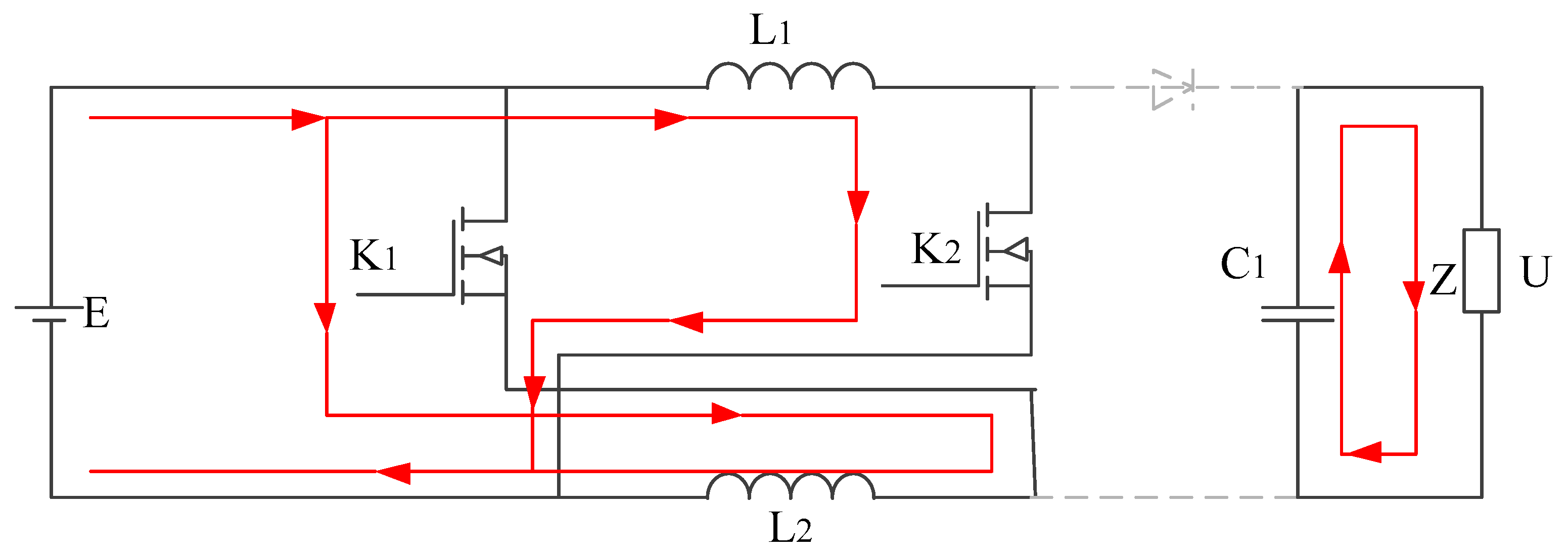
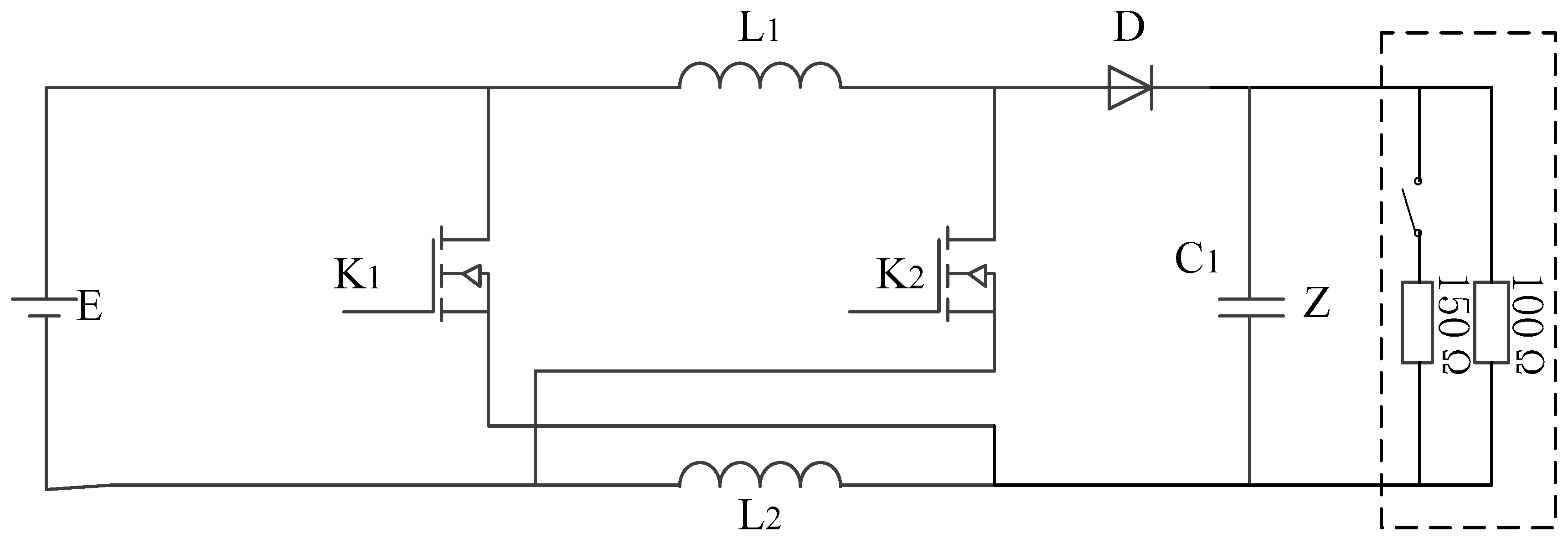
The dual-switch boost converter topology consists of two power switches K1, K2; two energy storage inductors L1, L2; a diode D, and an output filter capacitor C1. The two power switch devices are turned on or off simultaneously. The structure is simple, and the boost voltage is relatively high, which can meet the basic requirements of the DC/DC converter for fuel cell vehicles.
Assume that each component shown in Figure 1 is ideal. The inductance values of L1 and L2 are equal, and the parameters of the two MOSFETs K1 and K2 are equal and simultaneously turned on or off. In addition, the ON and OFF states of the MOSFETs correspond to different states.
When the switch is in the ON state, there are two current loops in the circuit, as shown in Figure 2. The parameters K1 and L2, K2 and L1 are connected in parallel with the input power source E to form the first loop. The filter capacitor C1 and load Z constitute a second loop. The turn-on voltage drop of the MOSFET is ignored. Inductors L1 and L2 are equivalent to two current sources, the voltage of which is the input supply voltage E. The direction of voltage and current is the associated reference direction, at which time the inductor absorbs energy. In one cycle TS, the two switches are turned on for D × TS, where D is the duty cycle of the PWM. If the inductor current is assumed to be constant, then IL1 = IL2 = IL. The energy absorbed by the inductors L1 and L2 is given by:
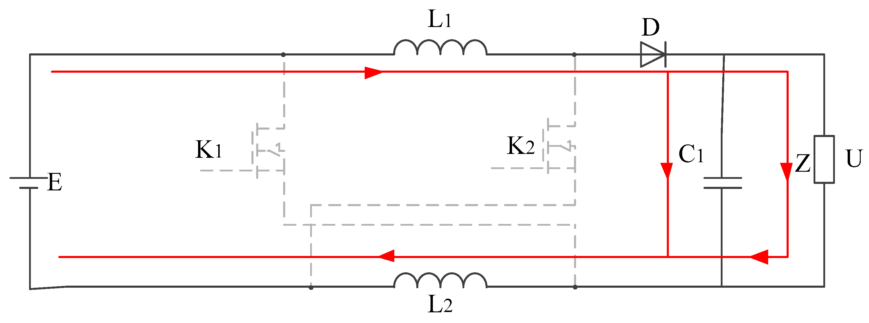
When the switch device is in the OFF state, the input power source E, the inductors L1 and L2 are connected in series. Energy is supplied to the filter capacitor C1 and the load through the diode D, and the capacitor replenishes energy.
The working mode of the dual-switch boost converter when the MOSFET is turned off is shown in Figure 3. At this time, there is a current loop in the circuit, that is, the inductors L1 and L2, the input power source E, the diode D, the filter capacitor C1, and the load constitute a loop. The voltage directions of the inductors L1 and L2 are not correlated with the current direction, at which time energy is released. The energy released by each inductor is given by:
According to the conservation of energy, the energy absorbed and released by the inductor in one PWM cycle is equal:
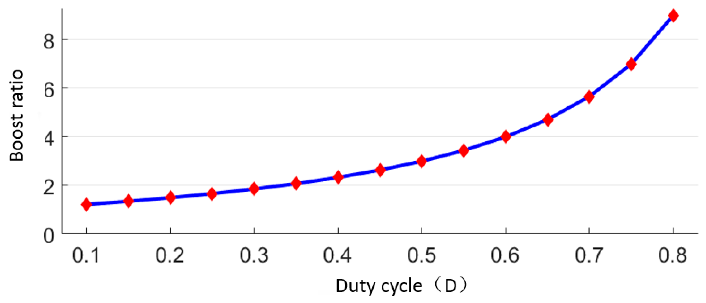
After simplification, the voltage gain of the dual-switch boost DC/DC converter under ideal conditions is:
From Equation (4) of the dual-switch boost converter, the relationship curve between the duty cycle of the switch and the boost ratio of the converter can be obtained, as shown in Figure 4.
2.2. Converter Mode of Operation
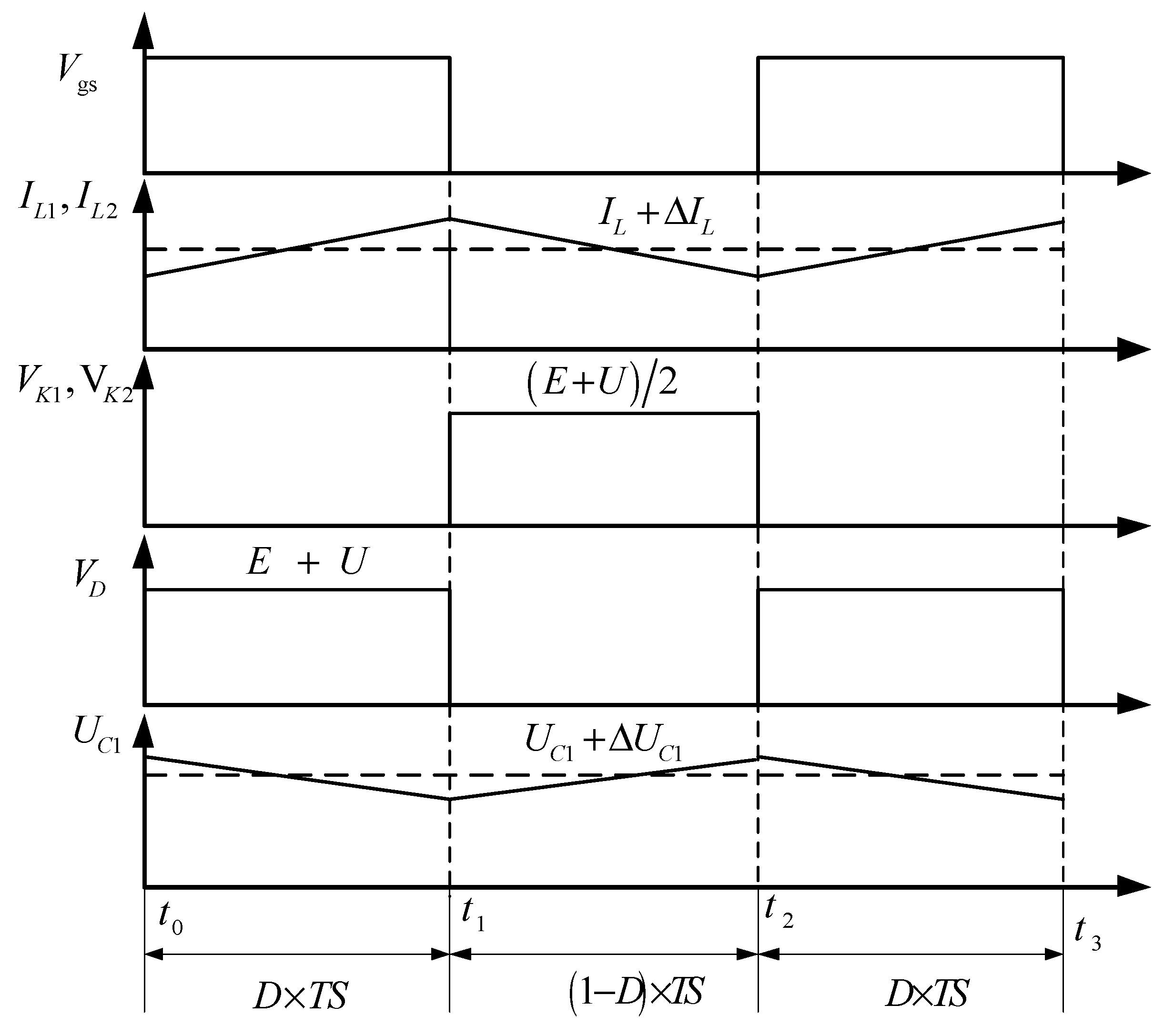
To further analyze the working mode of the dual-switch boost converter, this study establishes a state equation. The influence of inductor current fluctuations and capacitor voltage fluctuations on the circuit should be considered when establishing the equation of state. Figure 5 shows a waveform diagram during the operation of the dual-switch boost converter.
In Figure 5, the t0–t1 stage is the ON stage of the K1 and K2 MOSFETs. At this stage, the diode D is in the cut-off state, and the voltage stress is E + U. The voltage at both ends of inductors L1 and L2 is the input voltage E, and the inductor current increases linearly because the filter capacitor supplies energy to the load separately. Therefore, the capacitor voltage is reduced. Taking inductance L1 as an example, the current changes in this state are expressed as follows:
When t = D × TS, the current of inductors L1 and L2 is the maximum, and the current changes as follows:
The voltage change of capacitor C1 is expressed as follows:
The equation of state can be expressed as follows:
The working waveform of the MOSFET circuit is in the OFF state from t1 to t2. Diode D is turned on, and the inductance and input voltage simultaneously provide energy to the load and filter capacitor. At this stage, the inductance current can be expressed as follows:
At this stage, the inductance current decreases to the lowest value, and the current changes as follows:
The voltage of capacitor C1 will be increased because of the energy supplement. The voltage equation of capacitor C1 is as follows:
This stage is represented by the equation of state as follows:
3. Modeling of DC/DC Converters for Fuel Cell Vehicles
To design the control system of the proposed double-switching device boost DC/DC converter, a small signal model of the DC/DC converter is established in this study [23]. In the PWM cycle, the average state space equation of the DC/DC converter for the fuel cell is obtained using the state space averaging method [24,25]:
In Equation (13), represents the average of the duty ratios in one cycle. represent the average value of the inductor current, input voltage, and output voltage, respectively, in one cycle. When establishing the small-signal model, each average quantity is a superposition of the DC steady-state quantity and the AC small-signal. It can be expressed as follows:
where D, U, E, and IL1 are DC steady-state quantities, and , , , and denote the amount of AC small signal disturbance. Substituting Equation (14) into Equation (13) gives:
Ignoring the second-order infinitesimal, the DC steady-state model of the dual-switch boost converter is expressed as:
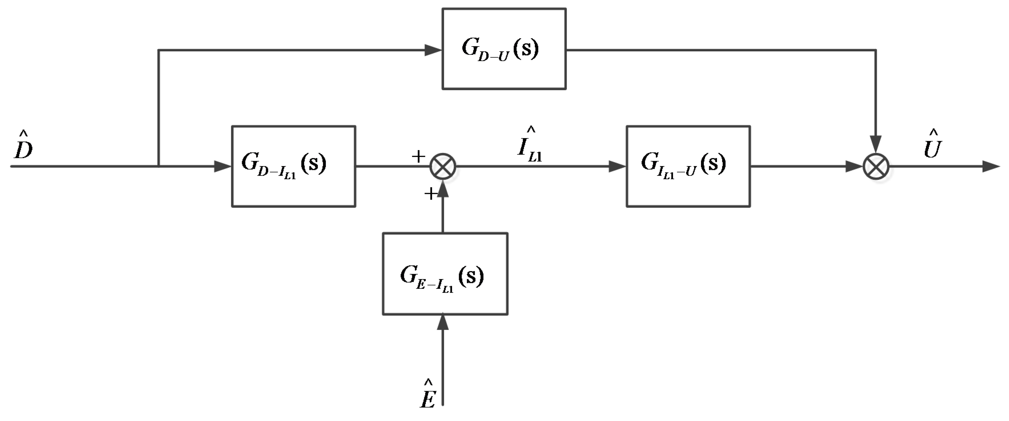
It can be seen from Equation (16) that the small signal of output voltage U and inductor current IL1 is not only affected by self-fluctuation but also by input voltage fluctuation and duty cycle fluctuation.
The AC small-signal model of the dual-switch boost converter can be established as follows:
Taking the Laplace transform for Equation (17), we obtain:
It can be seen from Equations (18) and (19) that the transfer function of duty cycle D to inductor current IL1 is:
The transfer function of input voltage E to output inductor current IL1 is:
The transfer function of inductor current IL1 to output voltage U is:
The transfer function from duty cycle D to output voltage U is:
The small signal model of the dual-switch boost converter is shown in Figure 6.
4. Feedforward Compensation of DC/DC Converter-Double Feedback Controller Design
To improve the robustness of the fuel cell DC/DC converter, based on the small signal model of the DC/DC converter, a double closed-loop control system based on output voltage and current is designed, and the output voltage closed-loop control system is compared with static characteristics, dynamic characteristics (stability time, overshoot) and anti-interference ability.
The process of designing the controller is as follows:
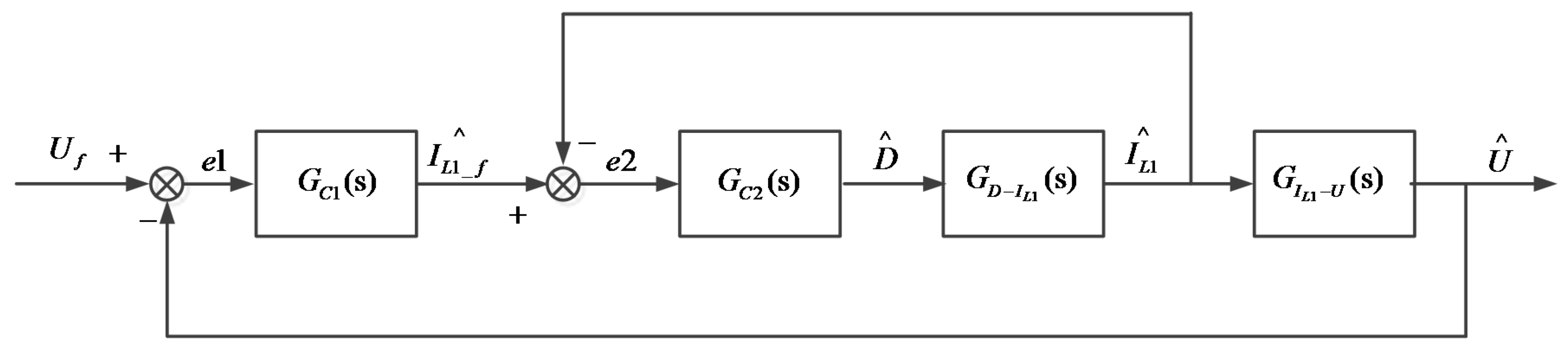
Setting the output reference voltage and comparing with the converter output voltage collected by the voltage sensor to obtain a voltage error signal. The voltage error signal is sent to the voltage loop PI controller for processing to obtain the desired inductor current . Then compare it with the converter inductor current collected by the current sensor to obtain a current error signal. The current error signal is sent to the current loop PI controller to obtain the adjusted duty ratio D. The duty ratio D after setting is fed into the transfer function to get the adjusted inductor current. Then, the adjusted inductor current is sent to the transfer function to obtain the adjusted output voltage.
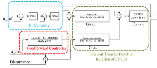
The block diagram of the designed double closed-loop control system is shown in Figure 7.
It can be seen from Figure 7 that the error e1 of the output voltage with respect to the reference voltage passes through the controller GC1 to obtain the reference amount of the inductor current. The error e2 of the inductor current with respect to its reference amount passes through the controller GC2 to obtain the control amount .
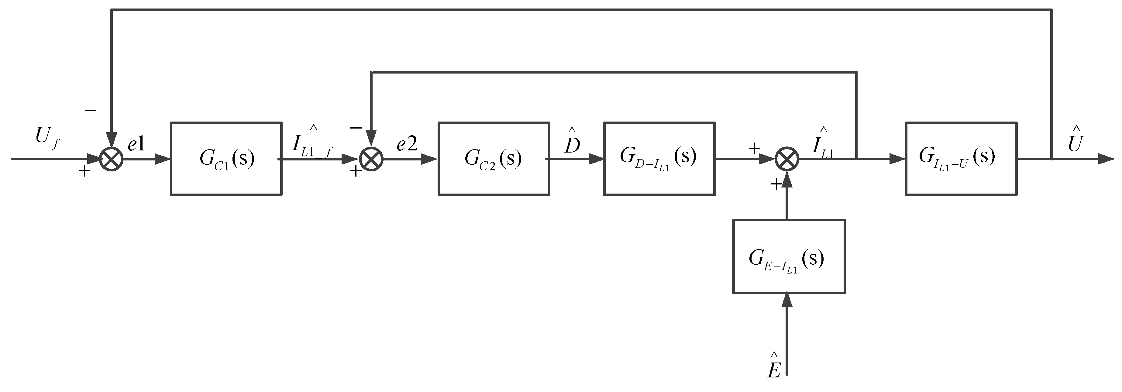
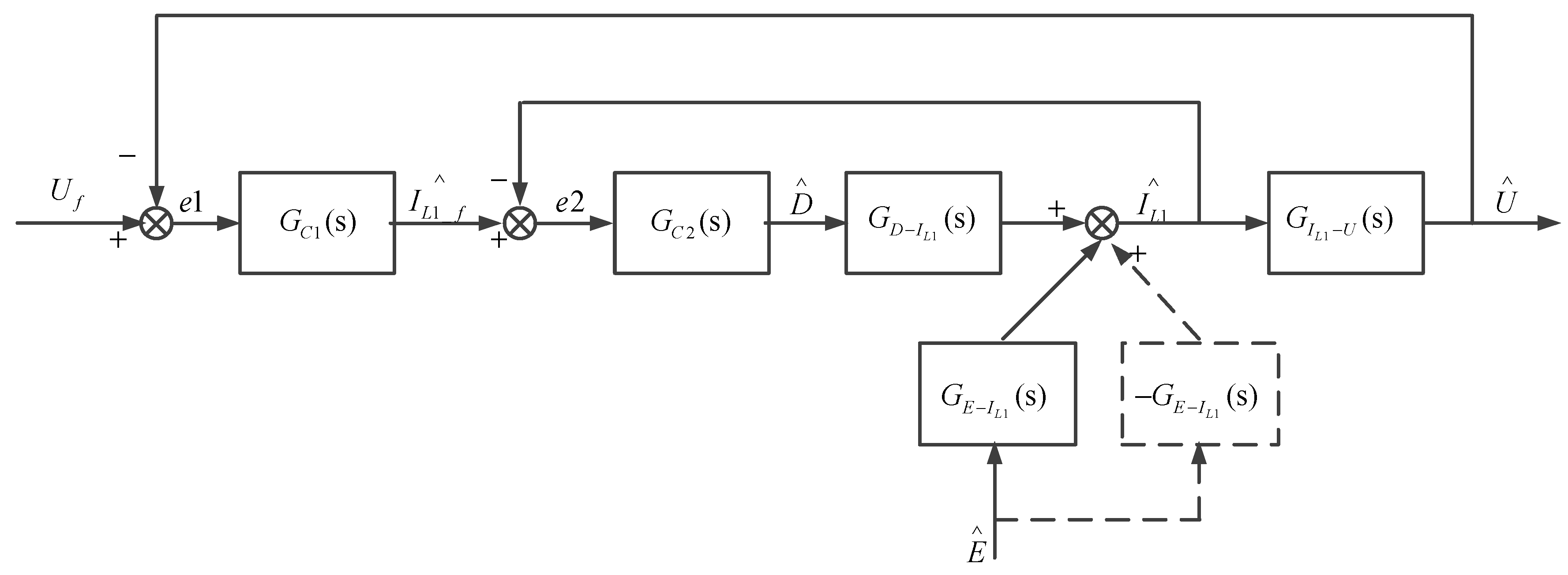
It can be seen from the small signal model shown in Figure 6 that not only the duty cycle D has an effect on the system output but also the input voltage E is equally disturbing to the system. If the influence of input voltage on system disturbance is considered, the structure of the double closed-loop control system can be further represented as shown in Figure 8.
It can be seen from Figure 8 that when the system reaches steady state, if the input voltage fluctuates, it will directly act on the system until the output change of the system is fed back to the control terminal, then the duty cycle D is adjusted and the output voltage tends to be stable. Because the output characteristics of the fuel cell are soft, that is, the fluctuation of the input power source E of the DC/DC converter is relatively frequent, it is necessary to increase the feedforward control for the input voltage variation to offset its influence on system disturbance.
To this end, this study proposes a compensation from the input voltage E in parallel to eliminate the influence of the fluctuation of the input voltage on the system. The corresponding control block diagram is shown in Figure 9.
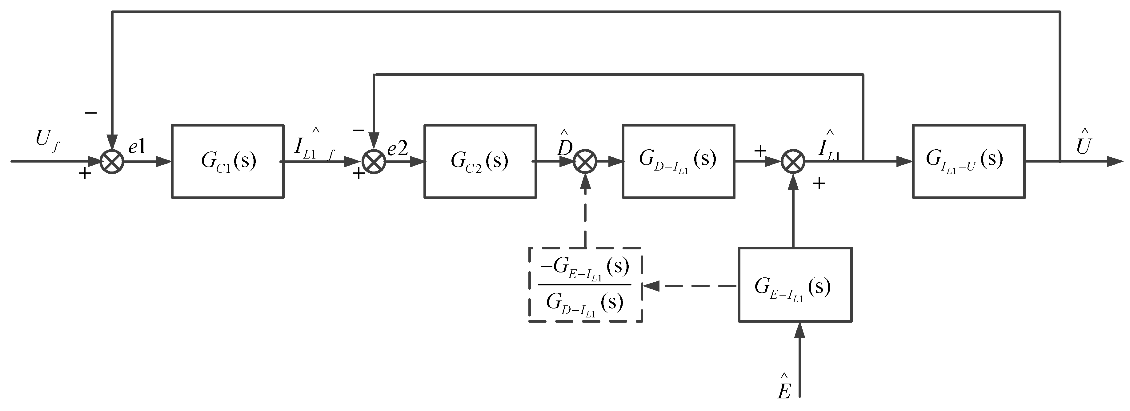
In actual control, the output voltage and current can only be controlled by adjusting the duty cycle of the PWM. Therefore, in the control block diagram shown in Figure 7, the compensation method has certain difficulty for introduction in engineering applications. To this end, this study transforms the control system with compensation shown in Figure 9, and its control system block diagram is shown in Figure 10.
Bring in Equations (20) and (21), deduce:
In Equation (24), inductance L is 3.5 mH, capacitance C is 47 µF, and resistance Z is 100 Ω.
5. Simulation and Experimental Results Analysis
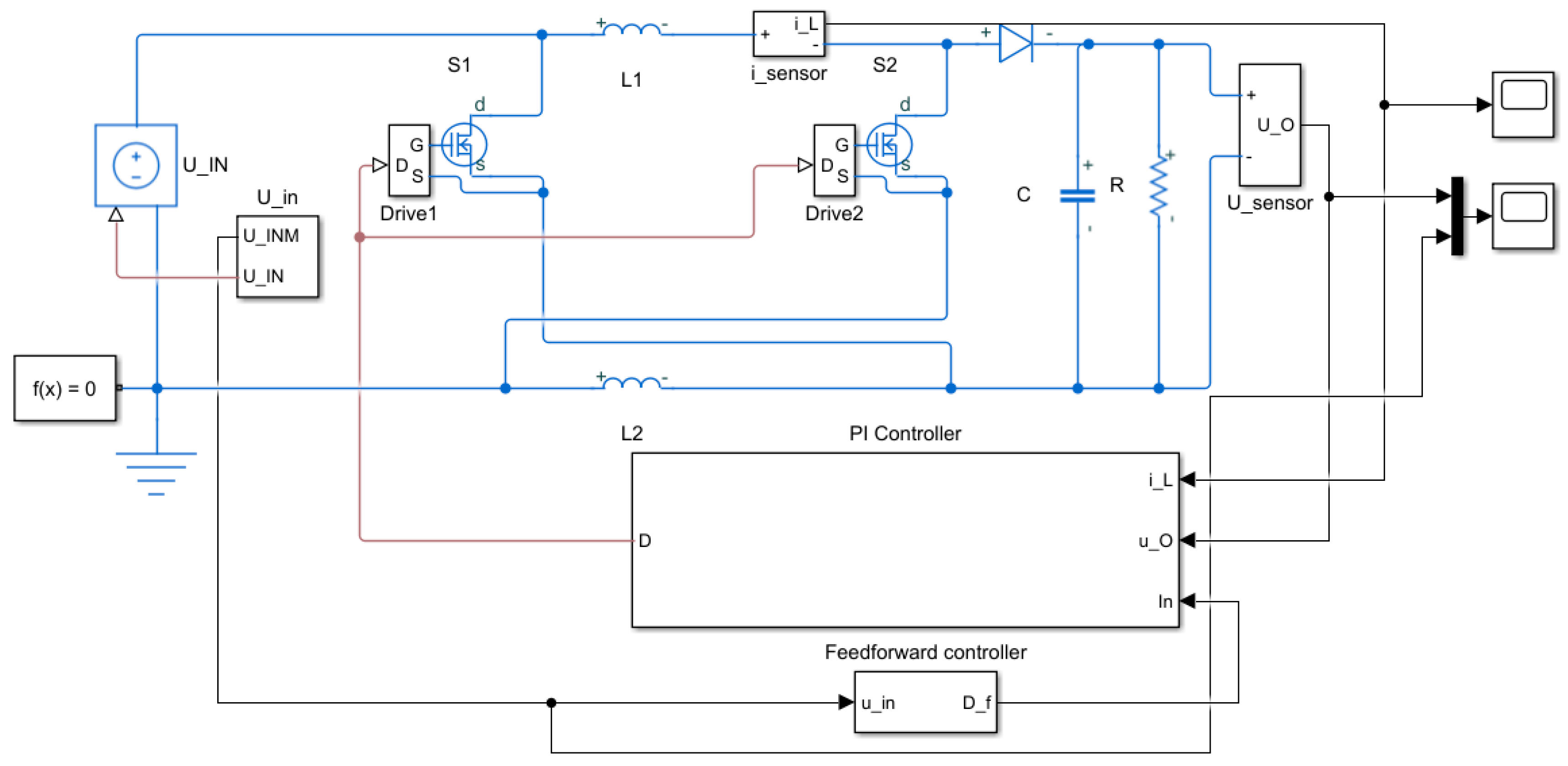
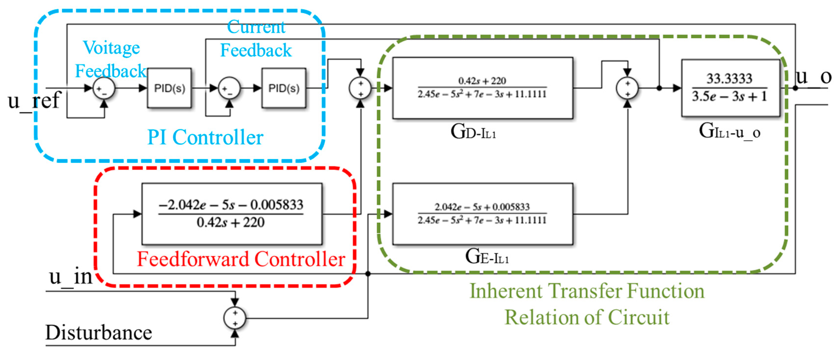
To verify the effectiveness of the proposed feedforward-double feedback control strategy, the PI parameters are adjusted using MATOTOOL, a toolbox provided by Matlab. Equation (24) is obtained using Equations (20) and (21), and the transfer function required for feedforward control is determined. The specific process capacities are shown in Figure 8, Figure 9 and Figure 10. A simulation model is built in Simscape, as shown in Figure 11. The details of the PI controller and feed-forward controller modules are shown in Figure 12, and the corresponding device parameters are listed in Table 1.
In this paper, the extended response curve method is used to tune PI parameters. Firstly, the system is in manual state. When the system reaches equilibrium near a given value, a step input signal is added to the system to obtain the response curve of the system to the step function. Obtain the equivalent pure lag time Tm, time constant of the controlled object τ according to the response curve at the maximum slope. Then expand the corresponding curve table by query to get the corresponding PI parameters, and finally test to make the system in the best state.
The voltage loop transfer function and current loop transfer function of double closed-loop PI controller are considered as a whole. The input and output of the double closed-loop controller are R(S) and D(S), the overall transfer function of the double closed-loop PI controller obtained is shown in Equation (25):
where is the output voltage, is the inductor current, and are the voltage loop PI parameters, and are the current loop PI parameters.
According to the obtained PI parameter value, the S domain transfer function of the double closed loop PI controller is pushed and Z-transformed. The resulting Z-domain transfer function of the double closed-loop PI controller is as shown in Equation (26):
where R(Z) is the input of the double closed loop PI controller, D(Z) is the output of the double closed loop PI controller.
The inverse transformation of Z for Equation (26) yields the expression of the discrete double closed-loop PI controller as follows:
The Z domain transfer function of the feedforward controller is shown in Equation (28):
where E(Z) is the input of the Feedforward controller, D(Z) is the output of the Feedforward controller.
Perform the inverse transformation of Z on Equation (3) to obtain the expression of the discrete feedforward controller as follows:
On this basis, real-time control of the controller is realized.
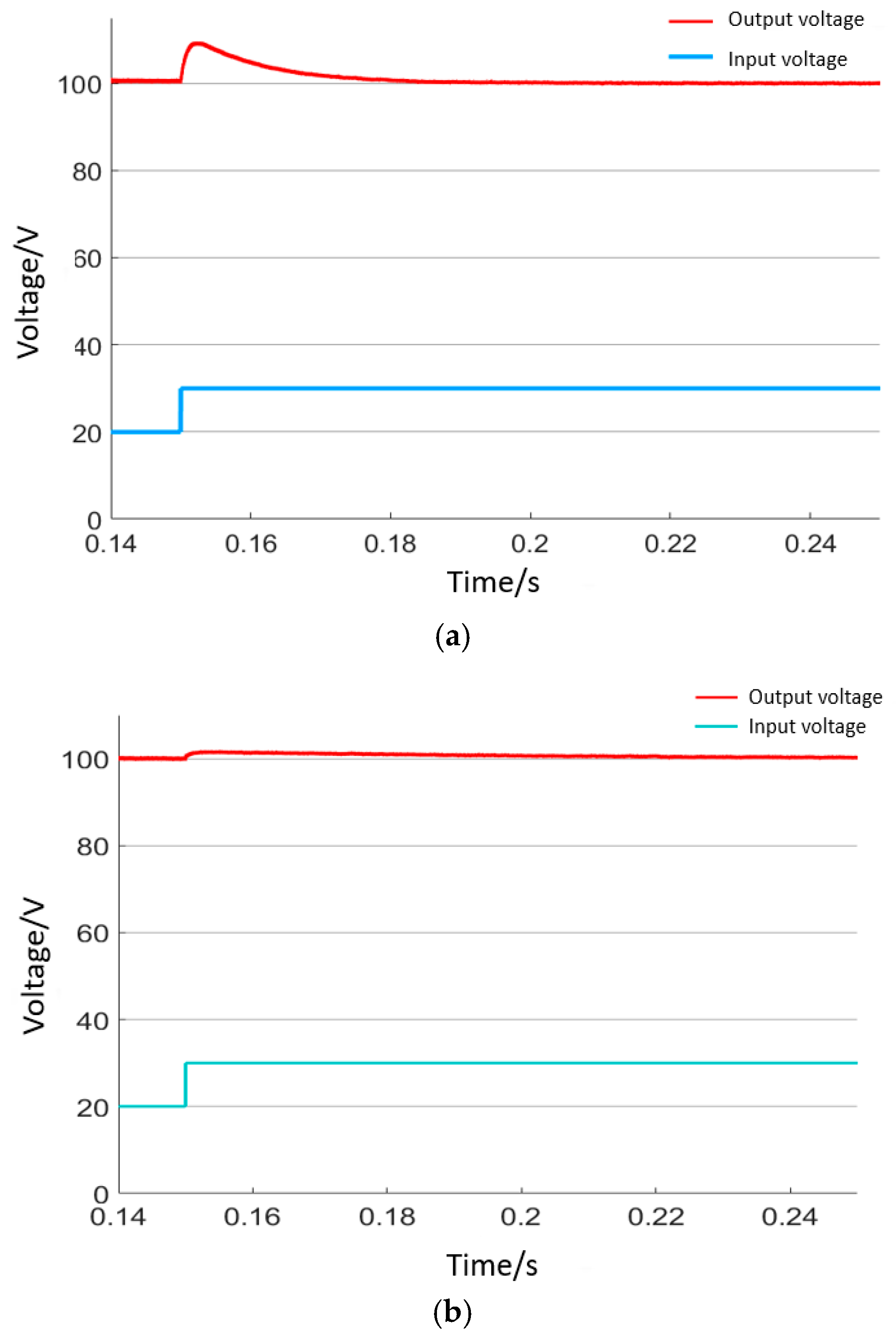
The input voltage is 20 V, the output voltage is 100 V, the load resistance is 100 Ω and the switching frequency is 20 kHz. The input voltage of the fuel cell can suddenly change to 30 V at 0.15 s after the operation of the system to simulate the output of the fuel cell. Furthermore, the DC/DC converter topology and the proposed feed-forward-double feedback control are verified to be suitable for fuel cell vehicles. On this premise, the output voltage waveforms of feedforward-double feedback control and voltage feedback control are studied and compared respectively, as shown in Figure 13.
As can be seen from Figure 13, when the input voltage is suddenly disturbed, the system output voltage fluctuation using voltage feedback control strategy is about 6 V, and the voltage fluctuation time is about 0.03 s. On the other hand, using the feedforward-double feedback control strategy proposed in this paper, the output voltage fluctuation of the system is about 2 V and the regulation time is about 0.01 s. Hence, the output voltage fluctuation of the feedforward-double feedback control proposed in this paper is one third of that of the voltage feedback control, and the time to restore stability after fluctuation is also one third of that of the voltage feedback control.
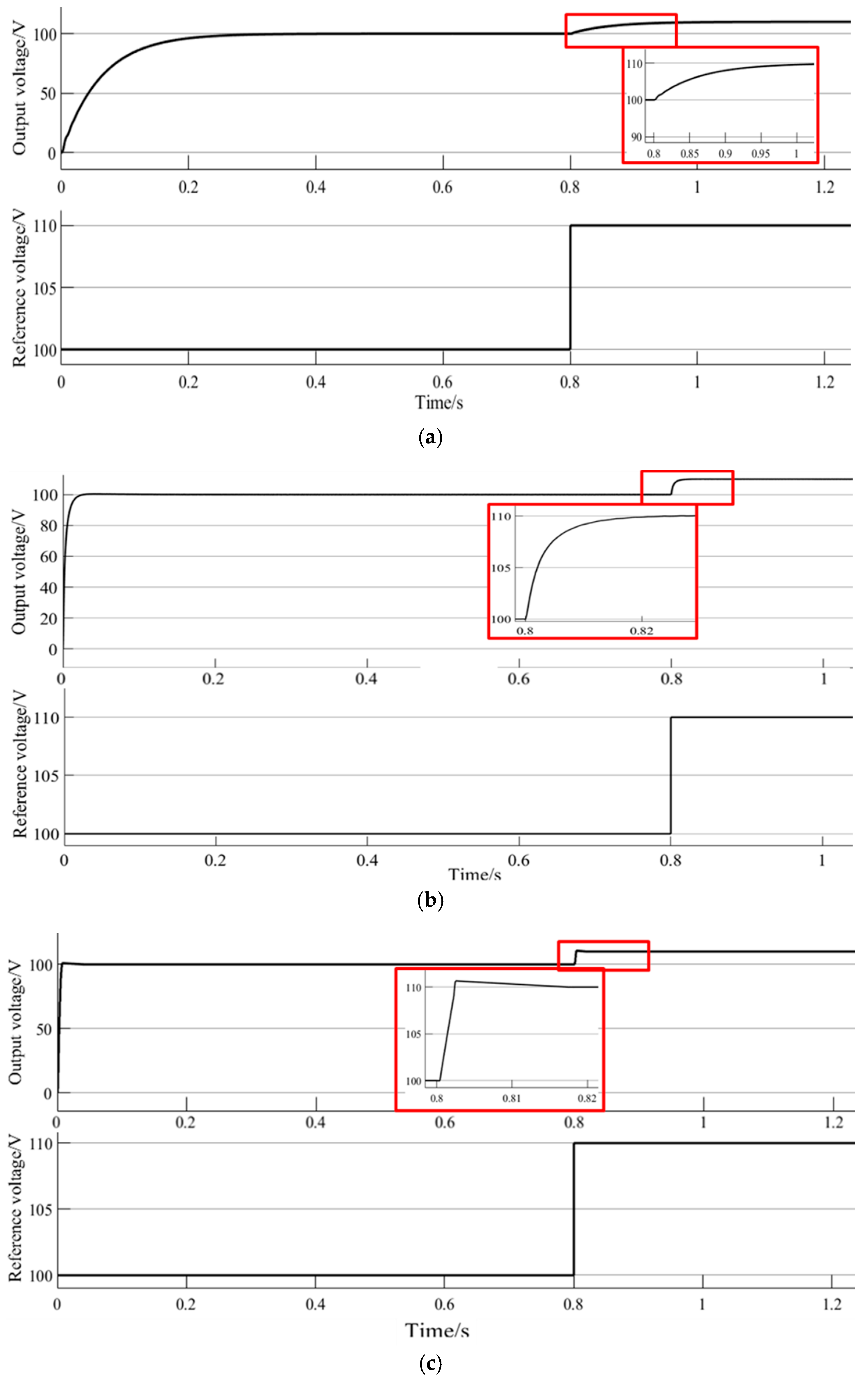
Setting the input voltage to 20 V, the output voltage to 100 V, and the switching frequency to 20 kHz, and considering that the output voltage will abruptly change to 110 V at 0.8 s after the system starts running, the output voltage waveforms of the voltage feedback control, the feedforward-double feedback control and sliding mode control are tested and compared, as shown in Figure 14.
As can be seen from Figure 14, based on the average state space model of the dual-switch boost converter, these control methods can achieve effective control. However, the feedforward-double feedback control system has better control effect than the voltage feedback control system. The voltage feedback control system takes a long time to reach the steady state, and when the reference value suddenly increases, the time for the voltage feedback control system to reach the steady state is about 0.2 s. On the other hand, the time of reaching steady state for the feed-forward-double feedback control system is about 0.02 s, which is one tenth of that of the single closed-loop control system. The sliding mode control system achieves steady state at 0.016 s, and has a certain overshoot. Thus, the stabilization time of the feedforward-double feedback control system is slightly longer than that of the sliding mode control system. However, the feedforward-double feedback control model is simple and easy to operate, so it is more suitable for engineering applications.
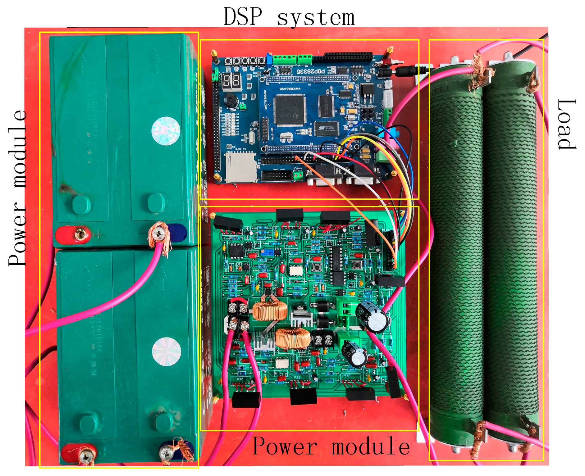
To further verify the effectiveness of the proposed method in engineering applications, a power module prototype based on the dual-switch boost converter topology is developed, as shown in Figure 15. Based on this, a comparative study of different control strategies is further carried out.
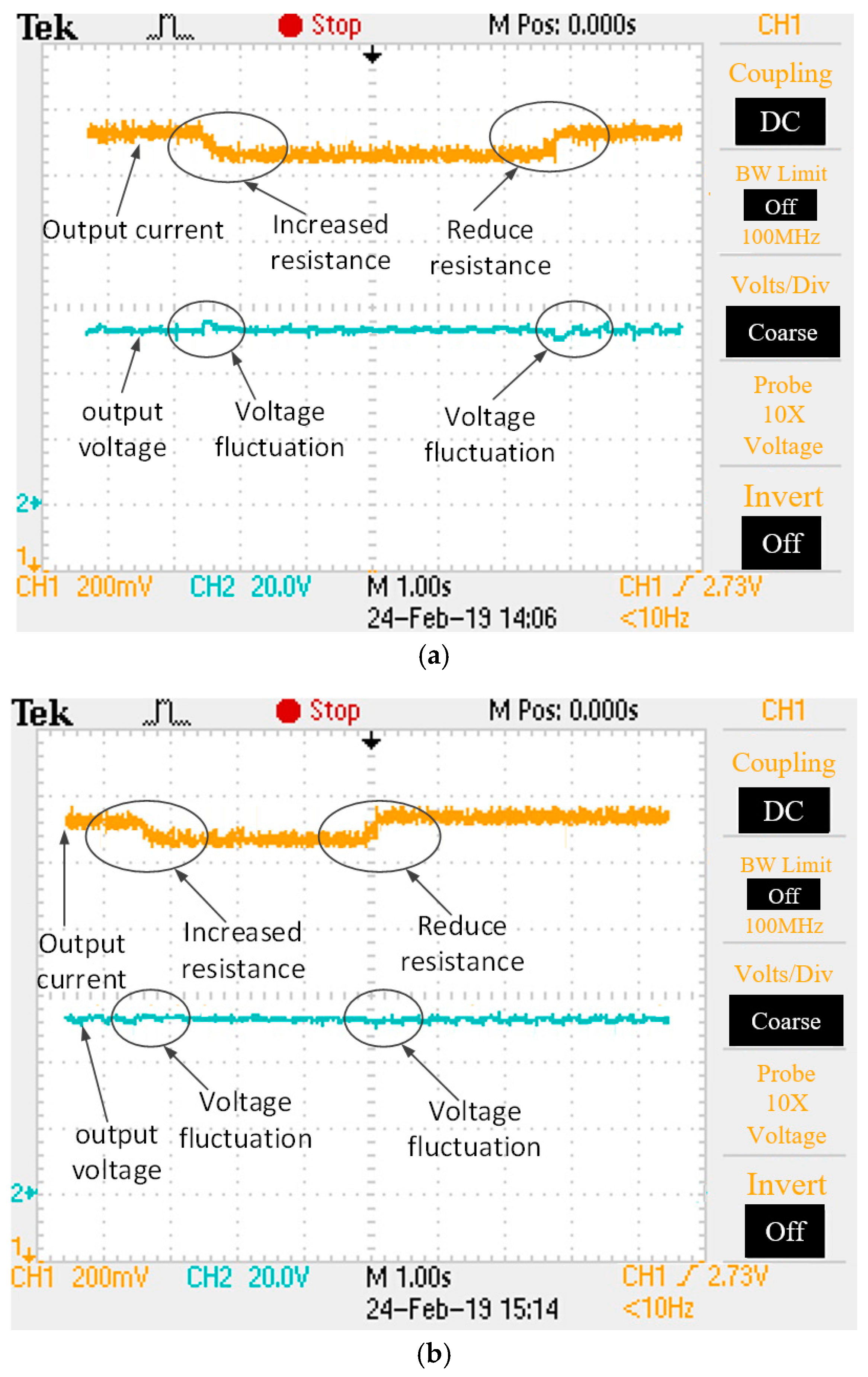
In order to verify the robustness of the proposed feed-forward-double feedback control method, load disturbance experiments are carried out. The schematic diagram of the designed load disturbance experiment is shown in Figure 16.
During the experiment, the input voltage was set to 24 V and the output voltage was 55 V. The feedforward-double feedback control is compared with the voltage feedback control. The result is shown in Figure 17. As can be seen from the experimental results, the actual output voltage of the two control methods is 54 V, the absolute error of the measurement is 1 V, and the relative error is 1.8%. With the feedforward-double feedback controller proposed in this paper, during the load switching process, the current decreases/increases by 0.36 A (after Hall sensor conversion), the increase/decrease of output current can reflect the increase/decrease of inductance current. The voltage fluctuation is almost unchanged. However, the voltage fluctuation of the voltage feedback controller output is 4 V. It can be seen that the proposed feedforward-double feedback controller has better robustness than the single feedback controller.
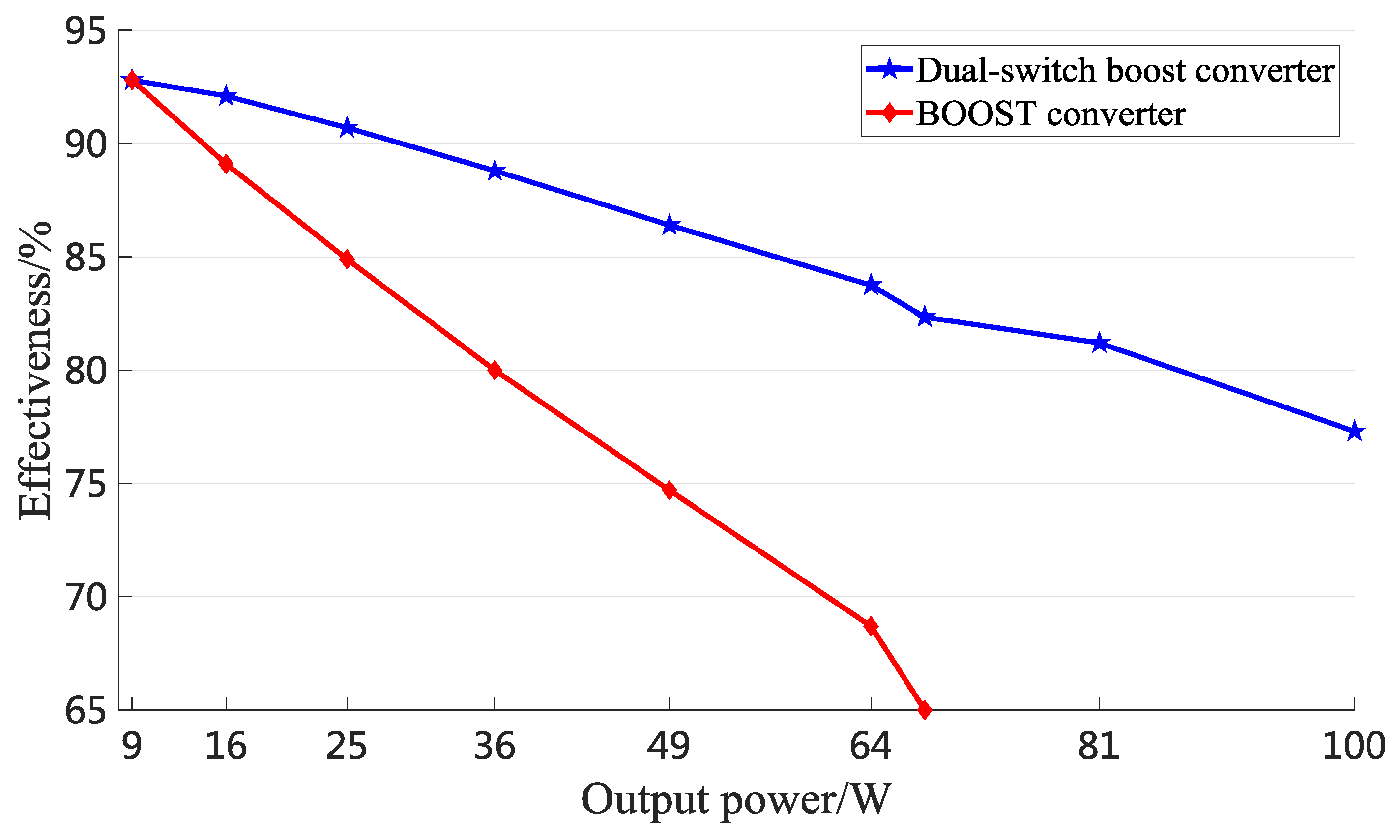
Setting the input voltage to 20 V and the load resistance to 100 Ω, the switching frequency is 20 kHz, and considering that the output voltage changes from 30 V to 100 V, the power of the system varies from 9 W to 100 W by calculation. We set the duty cycle to vary from 0.2 to 0.8. Therefore, the BOOST circuit can raise the voltage to 85 V because of its boost ratio; the maximum power of the BOOST circuit is 68 W. In this process, the efficiencies of the double-switch boost converter and BOOST converter are tested and compared. The main results are as follows:
As can be seen from Figure 18, with the proposed feedforward-double feedback control, the maximum and minimum efficiencies of the dual-switch boost DC/DC converter are 92.8% and 77.3%, respectively. The BOOST converter has a maximum efficiency of 92.5% and a minimum efficiency of 65.1%. When the output voltage increases, the duty cycle and inductance current increase, which leads to the increase of switching loss and inductance loss and hence the decrease of system efficiency. Compared with the BOOST circuit, the dual-switch boost converter has is advantageous in terms of conversion efficiency.
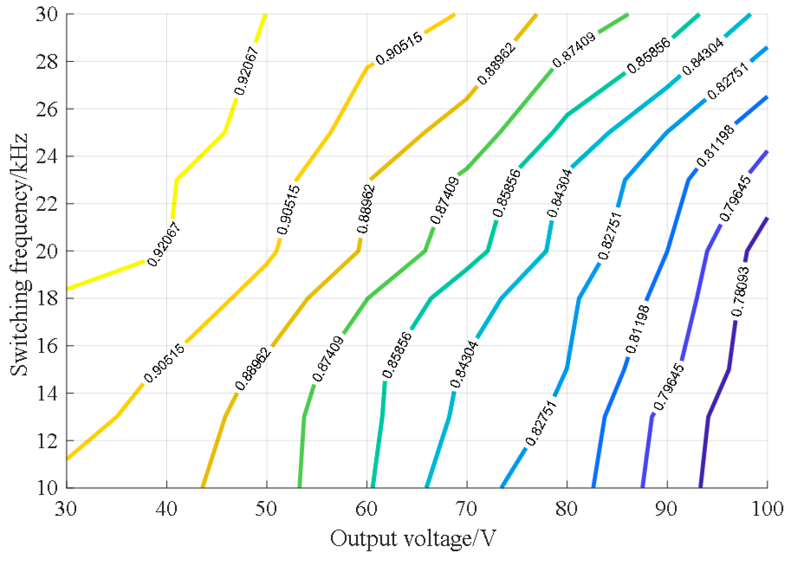
Setting the input voltage to 20 V and the load resistance to 100 Ω, and considering that the output voltage changes from 30 V to 100 V, the switching frequency changes from 10 kHz to 30 kHz, the efficiency of the system is tested under different situations. The efficiency map in terms of output voltage and switching frequency is shown as Figure 19. As can be seen from the figure, within the scope of the test, when the output voltage is fixed, the system efficiency increases as the switching frequency increases; when the switching frequency is fixed, the system efficiency increases as the output voltage decreases.
6. Conclusions
In order to solve the robustness problem of the DC/DC converter for fuel cell vehicles, based on a dual-switch boost DC/DC converter topology suitable for fuel cell automotive applications, a small-signal mathematical model that can reflect the operating characteristics of the converter is built by the state space averaging method. Under the premise of realizing double feedback control of DC/DC converter output voltage and current, by increasing the equivalent feedforward control link based on the disturbance voltage, the influence of the sudden change in voltage on system disturbance is effectively reduced. When the voltage disturbance and load are abrupt, the proposed feedforward-double feedback control system has strong robustness.
Author Contributions
J.D. guided the overall thinking of the paper and the design of the overall circuit. X.W. modeled the circuit and designed the controller. B.Y. built an experimental prototype for experimental verification and wrote the paper. W.S. checked and polished the paper.
Funding
This research received no external funding.
Acknowledgments
This work was sponsored through the National Key Technologies R&D Program of MOST (2018YFB0105403); State Key Laboratory of Automotive Safety and Energy under Project No. KF1826.
Conflicts of Interest
The authors declare no conflict of interest.
References
- Zhang, H.; Wang, J. Active Steering Actuator Fault Detection for an Automatically-Steered Electric Ground Vehicle. IEEE Trans. Veh. Technol. 2017, 66, 3685–3702. [Google Scholar] [CrossRef]
- Kommuri, S.K.; Defoort, M.; Karimi, H.R.; Veluvolu, K.C. A robust observer-based sensor fault-tolerant control for PMSM in electric vehicles. IEEE Trans. Ind. Electron. 2016, 63, 7671–7681. [Google Scholar] [CrossRef]
- Xu, L.; Fang, C.; Li, J.; Ouyang, M.; Lehnert, W. Nonlinear dynamic mechanism modeling of a polymer electrolyte membrane fuel cell with dead-ended anode considering mass transport and actuator properties. Appl. Energy 2018, 230, 106–121. [Google Scholar] [CrossRef]
- Chen, J.; Song, Q. A decentralized dynamic load power allocation strategy for fuel cell/supercapacitor -based APU of large more electric vehicles. IEEE Trans. Ind. Electron. 2019, 66, 865–875. [Google Scholar] [CrossRef]
- Wi, S.M.; Kim, M. Precise control strategy of dual-mode flyback DC/DC converter. IET Power Electron. 2019, 12, 220–227. [Google Scholar] [CrossRef]
- Wu, Y.; Huangfu, Y.; Ma, R.; Ravey, A.; Chrenko, D. A strong robust DC-DC converter of all-digital high-order sliding mode control for fuel cell power applications. J. Power Sources 2019, 413, 222–232. [Google Scholar] [CrossRef]
- Bi, H.K.; Wang, P.; Che, Y. A capacitor clamped H-type boost DC-DC converter with wide voltage-gain range for fuel cell vehicles. IEEE Trans. Veh. Technol. 2019, 68, 276–290. [Google Scholar] [CrossRef]
- Banaei, M.R.; Sani, S.G. Analysis and implementation of a new SEPIC-based single-switch buck-boost DC-DC converter with continuous input current. IEEE Trans. Power Electron. 2018, 33, 10317–10325. [Google Scholar] [CrossRef]
- Zhang, Y.; Zhou, L.; Sumner, M.; Wang, P. Single-Switch, Wide Voltage-Gain Range, Boost DC-DC Converter for Fuel Cell Vehicles. IEEE Trans. Veh. Technol. 2018, 67, 134–145. [Google Scholar] [CrossRef]
- Wu, Q.; Wang, Q.; Xu, J.; Xiao, L. Implementation of an Active-Clamped Current-Fed Push-Pull Converter Employing Parallel-Inductor to Extend ZVS Range for Fuel Cell Application. IEEE Trans. Ind. Electron. 2017, 64, 7919–7929. [Google Scholar] [CrossRef]
- Wang, P.; Zhou, L.; Zhang, Y.; Li, J.; Sumner, M. Input-Parallel Output-Series DC-DC Boost Converter with a Wide Input Voltage Range, For Fuel Cell Vehicles. IEEE Trans. Veh. Technol. 2017, 66, 7771–7781. [Google Scholar] [CrossRef]
- Sathyan, S.; Suryawanshi, H.; Singh, B. ZVS-ZCS High Voltage Gain Integrated Boost Converter for DC Microgrid. IEEE Trans. Ind. Electron. 2016, 63, 6898–6908. [Google Scholar] [CrossRef]
- Zheng, Y.; Ho, M.; Guo, J.; Leung, K.N. A Single-Inductor Multiple-Output Auto-Buck-Boost DC-DC Converter with Tail-Current Control. IEEE Trans. Power Electron. 2016, 31, 7857–7875. [Google Scholar] [CrossRef]
- Rajaei, A.; Khazan, R.; Mahmoudian, M.; Mardaneh, M.; Gitizadeh, M. A dual inductor high step-up DC/DC converter based on the Cockcroft-walton multiplier. IEEE Trans. Power Electron. 2018, 33, 9699–9709. [Google Scholar] [CrossRef]
- Talebi, S.; Adib, E.; Delshad, M. A high gain soft switching interleaved DC-DC converter. IEICE Trans. Electron. 2018, E101-C, 906–915. [Google Scholar] [CrossRef]
- An, F.; Song, W.; Yu, B.; Yang, K. Model Predictive Control with Power Self-Balancing of the Output Parallel DAB DC–DC Converters in Power Electronic Traction Transformer. IEEE J. Emerg. Sel. Top. Power Electron. 2018, 6, 1806–1818. [Google Scholar] [CrossRef]
- Saadatizadeh, Z.; Heris, P.C.; Babaei, E.; Sabahi, M. A new nonisolated single-input three-output high gain converter with low voltage stresses on switches and diodes. IEEE Trans. Ind. Electron. 2019, 66, 4308–4318. [Google Scholar] [CrossRef]
- Farakhor, A.; Abapour, M.; Sabahi, M. Design, Analysis, and implementation of a multiport DC-DC converter for renewable energy applications. IET Power Electron. 2018, 12, 465–475. [Google Scholar] [CrossRef]
- Hebala, O.M.; Aboushady, A.A.; Ahmed, K.H.; Abdelsalam, I. Generic Closed-Loop Controller for Power Regulation in Dual Active Bridge DC-DC Converter with Current Stress Minimization. IEEE Trans. Ind. Electron. 2019, 66, 4468–4478. [Google Scholar] [CrossRef]
- Villarruel-Parra, A.; Forsyth, A.J. Modeling Phase Interactions in the Dual-Interleaved Buck Converter Using Sampler Decomposition. IEEE Trans. Ind. Electron. 2019, 66, 3316–3322. [Google Scholar] [CrossRef]
- Yang, L.S.; Liang, T.J.; Chen, J.F. Transformerless DC–DC Converters with High Step-Up Voltage Gain. IEEE Trans. Ind. Electron. 2009, 56, 3144–3152. [Google Scholar] [CrossRef]
- Dhanalakshmi, S.U.R. A Transformerless Boost Converters with High Voltage Gain and Reduced Voltage Stresses on the Active Switches. Int. J. Sci. Res. Publ. 2014, 3, 1–8. [Google Scholar]
- Li, X.; Ruan, X.; Jin, Q.; Sha, M.; Tse, C.K. Small-Signal Models with Extended Frequency Range for DC–DC Converters with Large Modulation Ripple Amplitude. IEEE Trans. Power Electron. 2017, 33, 8151–8163. [Google Scholar] [CrossRef]
- Zhang, K.; Shan, Z.; Jatskevich, J. Large- and Small-Signal Average Value Modeling of Dual-Active-Bridge DC–DC Converter Considering Power Losses. IEEE Trans. Power Electron. 2016, 32, 1964–1974. [Google Scholar] [CrossRef]
- Villarruel-Parra, A.; Forsyth, A.J. Enhanced Average-Value Modeling of Interleaved DC-DC Converters Using Sampler Decomposition. IEEE Trans. Power Electron. 2016, 32, 2290–2299. [Google Scholar] [CrossRef]
Figure 1.
Dual-switch boost converter topology.

Figure 2.
Operating mode of a dual-switch boost converter when the MOSFET is in the ON state.

Figure 3.
Operating mode of a dual-switch boost converter when the MOSFET is in the OFF state.

Figure 4.
Relationship between the boost ratio of a dual-switch boost converter and duty cycle of MOSFET switch.
Figure 4.
Relationship between the boost ratio of a dual-switch boost converter and duty cycle of MOSFET switch.

Figure 5.
Working waveform of dual-switch boost converter.

Figure 6.
Small signal model of a dual-switch boost converter.

Figure 7.
DC/DC converter voltage-current double closed-loop control system.

Figure 8.
Control block diagram after adding input voltage disturbance.

Figure 9.
Dual feedback control flow chart for input voltage compensation.

Figure 10.
Feedforward-double feedback control flow chart.

Figure 11.
Dual-switch boost converter simulation model.

Figure 12.
Details of PI controller and feedback controller modules.

Figure 13.
Output voltage response when two different control strategies are used to handle input voltage disturbance. (a) Voltage feedback control system; and (b) feedforward-double feedback control system.
Figure 13.
Output voltage response when two different control strategies are used to handle input voltage disturbance. (a) Voltage feedback control system; and (b) feedforward-double feedback control system.

Figure 14.
System output response under different control strategies. (a) Voltage feedback control system output; (b) feedforward-double feedback control system output; and (c) sliding mode control system output.
Figure 14.
System output response under different control strategies. (a) Voltage feedback control system output; (b) feedforward-double feedback control system output; and (c) sliding mode control system output.

Figure 15.
Design power module prototype.

Figure 16.
Schematic diagram of load disturbance experiment.

Figure 17.
System output response under different control strategies. (a) Voltage feedback control system output; and (b) feedforward-double feedback control system output.
Figure 17.
System output response under different control strategies. (a) Voltage feedback control system output; and (b) feedforward-double feedback control system output.

Figure 18.
Efficiency comparison of two kinds of converters.

Figure 19.
The efficiency of the system under different situations.


Table 1.
Device parameters in the simulation model.
| Name | Parameter |
|---|---|
| MOSFET (IFR640N) | Breakdown voltage VDSS 200 V |
| Conducted resistance RDS (on) 0.15 Ω | |
| Source current IS 18 A | |
| Diode (DFE 10 I 600PM) | Maximum reverse voltage VRRM 600 V |
| Forward voltage drop VF 1.5 V | |
| Conduction internal resistance rF 28.7 mΩ | |
| Inductance | 3.5 mH |
| Capacitance | 47 μF |
© 2019 by the authors. Licensee MDPI, Basel, Switzerland. This article is an open access article distributed under the terms and conditions of the Creative Commons Attribution (CC BY) license (http://creativecommons.org/licenses/by/4.0/).
Share and Cite
MDPI and ACS Style
Wu, X.; Yu, B.; Du, J.; Shi, W. Feedforward-Double Feedback Control System of Dual-Switch Boost DC/DC Converters for Fuel Cell Vehicles. Energies 2019, 12, 2886. https://doi.org/10.3390/en12152886
AMA Style
Wu X, Yu B, Du J, Shi W. Feedforward-Double Feedback Control System of Dual-Switch Boost DC/DC Converters for Fuel Cell Vehicles. Energies. 2019; 12(15):2886. https://doi.org/10.3390/en12152886
Chicago/Turabian StyleWu, Xiaogang, Boyang Yu, Jiuyu Du, and Wenwen Shi. 2019. "Feedforward-Double Feedback Control System of Dual-Switch Boost DC/DC Converters for Fuel Cell Vehicles" Energies 12, no. 15: 2886. https://doi.org/10.3390/en12152886
Note that from the first issue of 2016, this journal uses article numbers instead of page numbers. See further details here.