A Hybrid Soft Switching Full Bridge Converter Suitable for the Electric Vehicle Charge Applications


Department of Electrical Engineering, Soongsil University, 369 Sangdo-ro, Seoul 06978, Korea
*
Author to whom correspondence should be addressed.
Energies 2019, 12(14), 2707; https://doi.org/10.3390/en12142707
Submission received: 24 June 2019
/
Revised: 9 July 2019
/
Accepted: 11 July 2019
/
Published: 15 July 2019
(This article belongs to the Special Issue Recent Power Electronics and Control Systems for (Plug-In) Electric (Hybrid) Vehicles)
Abstract
:A hybrid dc–dc converter suitable for the on-board charger applications consisted of a Soft Switching Full Bridge (SSFB) converter and a Half Bridge (HB) LLC resonant converter is proposed. The proposed topology employs an additional switch and a diode at the secondary of the SSFB converter to eliminate the circulating current and to achieve the full soft switching of the primary switches. The output voltage is regulated by adjusting the duty of the secondary side switch. The validity and feasibility of the proposed converter are verified by the experiments with a 10-kW prototype converter. The maximum of 96.8% efficiency is achieved at 5 kW output power.
1. Introduction
Recently, plug-in hybrid electric vehicles (PHEVs) and pure electric vehicles (EVs) have become a promising remedy for global warming and fossil fuel depletion [1,2,3,4]. In these vehicles, the energy storage system contains a high-energy density rechargeable battery pack which normally comprises of about 88 to 150 Li-ion batteries connected in series. This high-voltage battery pack is charged by the battery charger that can be classified into an on-board charger (OBC) mounted inside the vehicle and off-board charger (or fast charger) built in the charging station. The drawback of the OBC is that it takes a long time (5–8 h) to fully charge an EV’s battery while the off-board charger requires an expensive infrastructure of charging stations. There are various kinds of practical OBCs are available in the market [5,6]. Though the power rating of a typical Level 1 or Level 2 Charger does not exceed 6.6 kW, Tesla Motors has introduced their own OBC of which power rating is 11.5 kW [7].
There are several key objectives in the development of battery chargers such as high power density, lower weight, and maximized power conversion efficiency all over the load range of battery charging profile [8]. The most common OBCs are composed of an ac–dc converter and an isolated dc–dc converter [8,9,10,11]. The front end ac–dc converter converts ac to dc to make the dc bus from 360 V to 400 V. The rear-end dc–dc converter charges the EV battery of which output voltage ranges from 250 V to 450 V, typically. This research only focuses on the rear-end dc–dc converter with the 10-kW charging level.
Phase-shifted full bridge (PSFB) converters have been widely used in high power dc–dc application because of its high power capacity and ZVS realization of all switches without auxiliary circuit [12,13,14]. However, when taking into account the battery charger applications, PSFB has two major problems. Firstly, the ZVS range of the lagging-leg switches is limited due to the wide output power range. As the battery pack is nearly fully charged, the OBC circuit works under the constant voltage (CV) mode with a small cut-off charging current. Since the ZVS of the lagging-leg switches is performed by the stored energy of the leakage inductor, the lagging-switches loses ZVS at the light load. The second is the circulating energy issue causing conduction losses and hence the efficiency degradation.
Some solutions have been proposed to address limited ZVS range problem [15,16]. The range of the ZVS can be expanded by increasing the leakage inductance value of the transformer or by adding an external inductor connected in series with the transformer. However, a large leakage inductance or a series inductance prolongs the time required for the primary current to change its polarity from negative to positive, and vice versa. Hence, it causes a loss of effective duty cycle on the secondary side of the transformer and decreases the efficiency of the converter. Other techniques have been developed based on the current-enhancement principle. These techniques utilize the inductive energy stored in the additional auxiliary circuit instead of that in the leakage or the external series inductance to extend the ZVS range [17,18,19,20]. These methods cannot optimally resolve the trade-off between the power loss saved by the wide range of ZVS operation and the power losses caused by the auxiliary circuits for the EV battery charge applications, which requires a very wide load range operation and a wide duty cycle variation at the same time.
To cope with the circulating current issues, a method was introduced to reset the primary current [21]. The basic idea is to realize a blocking voltage source to make the primary current decay to zero in the zero state. In [22], a blocking capacitor is added in series with the primary winding transformer to reset the primary current during freewheeling intervals to ensure zero-current-switching (ZCS) for lagging leg switches. In [23], the blocking capacitor is transferred to secondary winding of transformer. An auxiliary circuit composed of a resonance capacitor and two diodes is added in the output side of PSFB converter. In addition to the ZCS capability, the capacitor can also contribute to clamping the voltage of the rectifiers.
The other topology is an LLC resonant converter which has very high efficiency characteristics at its resonant frequency. The most suitable application for the resonant converter is the bus converter which operates at the optimal point with minimal circulating loss to achieve a high efficiency. However, in case of the battery charger applications, since a wide variation in the input and output voltage is required, the switching frequency range becomes extremely wide, thereby making the resonant operation impractical. To overcome the variable frequency control problem, some research [24,25,26,27,28] has been conducted using the phase-shift control to operate the resonant converter with a fixed frequency.
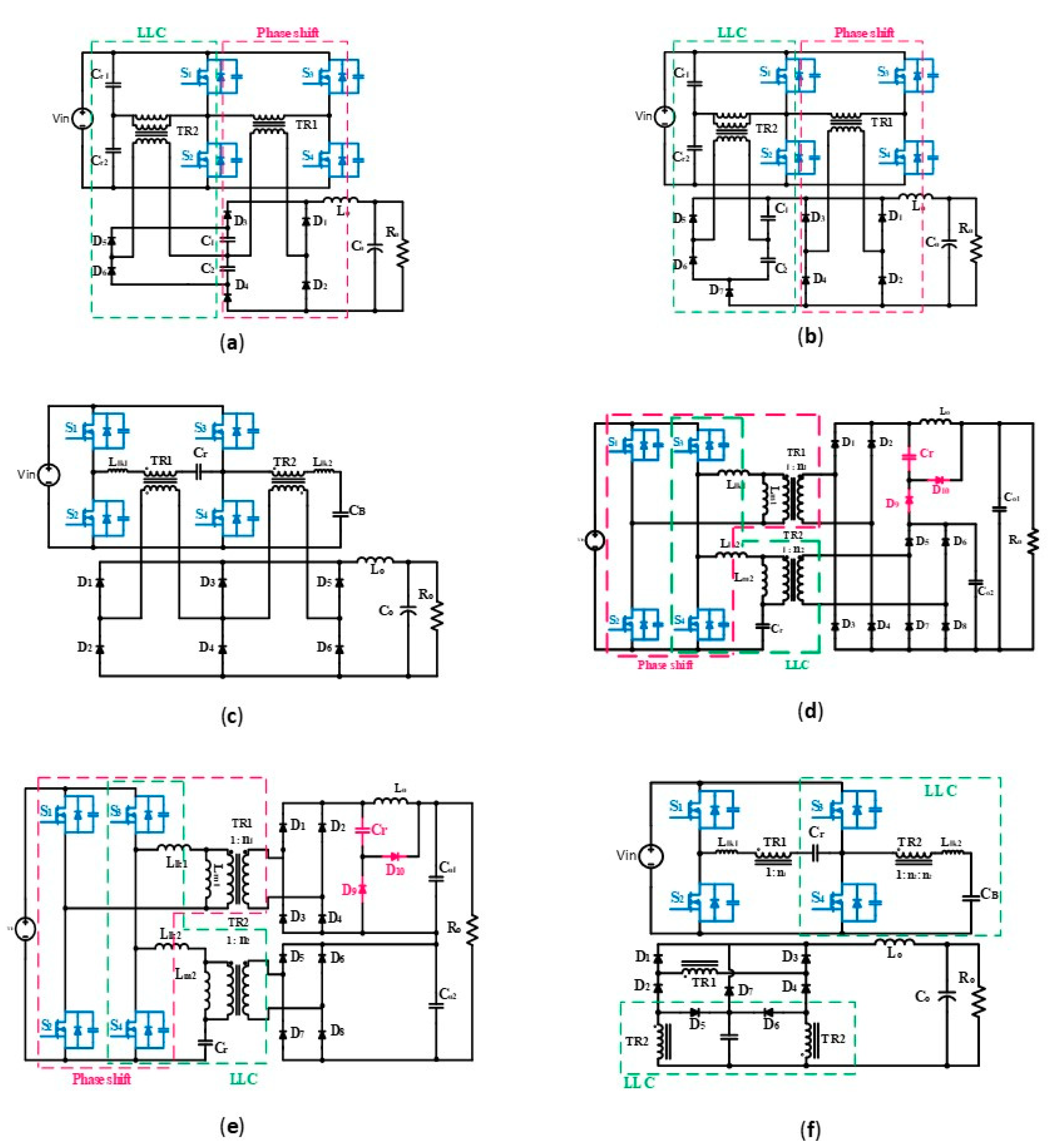
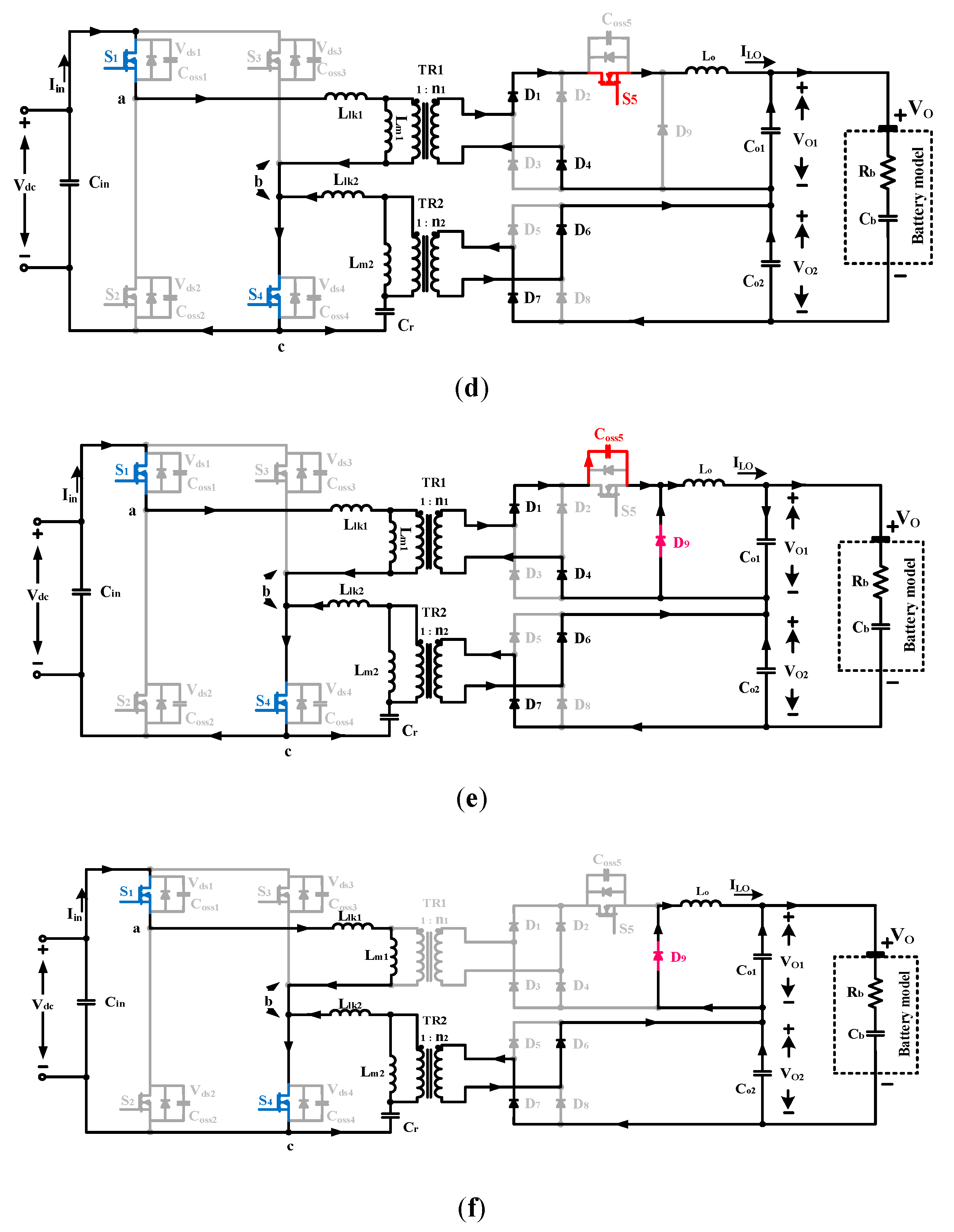
Some hybrid topologies which combine a phase-shift full bridge converter and an LLC resonant converter have been introduced in recent studies. The main concept of hybrid topology is sharing the primary side leg and the secondary side circuits are connected in series or parallel, as shown in Figure 1. The LLC converter operates at resonant frequency with unity voltage gain and transfers the energy to output during whole switching period while the output voltage is regulated by the phase-shift modulation method. By sharing the lagging leg switches, the ZVS range of lagging leg can be obtained from zero to full-load condition as shown in Figure 1a–c. In Figure 1d,e, a clamping circuit including Cr, D9, and D10 is employed to reset the circulating current and to damp the voltage oscillation across the secondary rectifier. Though the circulating current can be reduced as compared to the tradition phase-shift full-bridge converter, the lagging leg switches still suffer from hard switching turn-off.
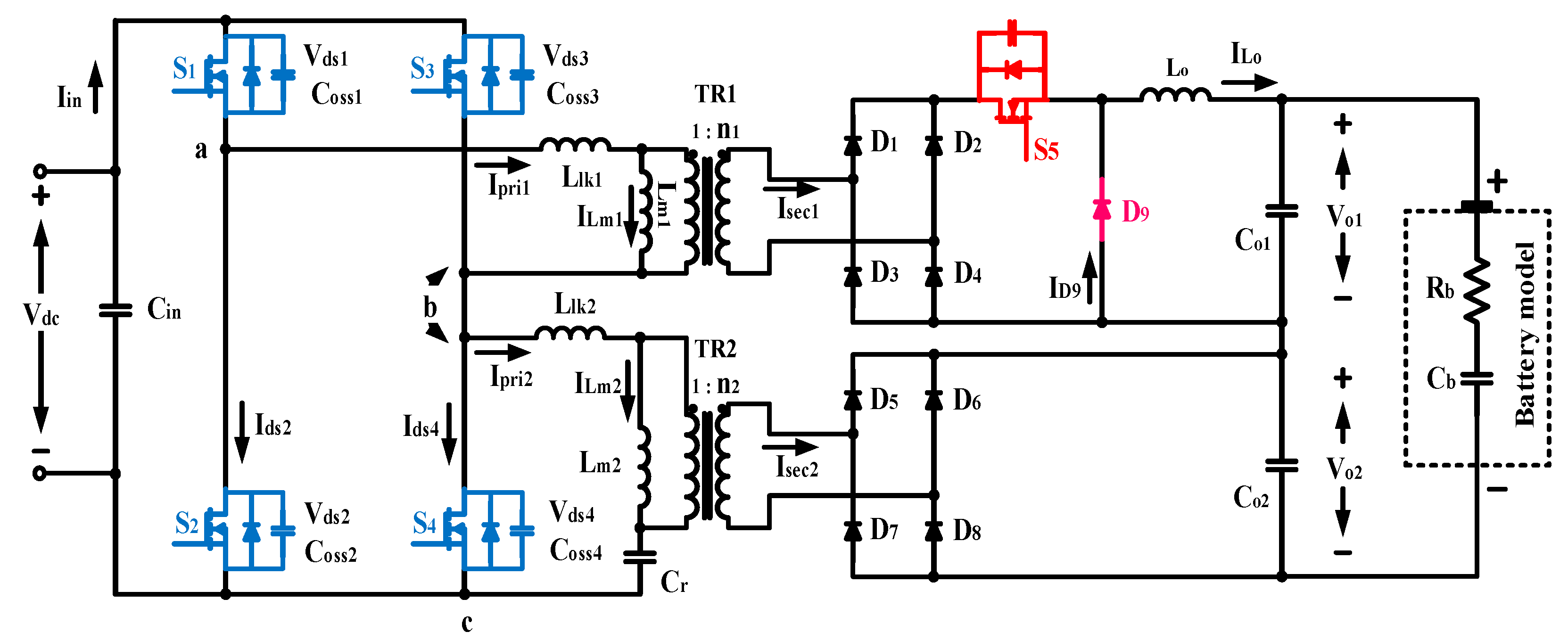
In this paper, a novel hybrid topology which combines a SSFB converter and a HB LLC converter is proposed as shown in Figure 2 [29]. In the SSFB topology, an additional switch and a freewheeling diode are employed on the secondary side to achieve following advantages: ZVS and ZCS of the primary switches, wide ZVS range, no circulating current, small passive components in the secondary and simple switching scheme.
This paper is structured as follow. In Section 2, the circuit description and the basic operation principles are introduced. In Section 3 the analysis of the proposed converter such as DC voltage gain and ZVS condition for the primary switches under full range of load are given. In Section 4, a design example is explained before presenting a 10-kW hardware prototype in Section 5. The experimental results demonstrate that the proposed converter can get high efficiency. Finally, the concluding remarks are given in Section 6.
2. Operation Mode of the Proposed Hybrid Converter
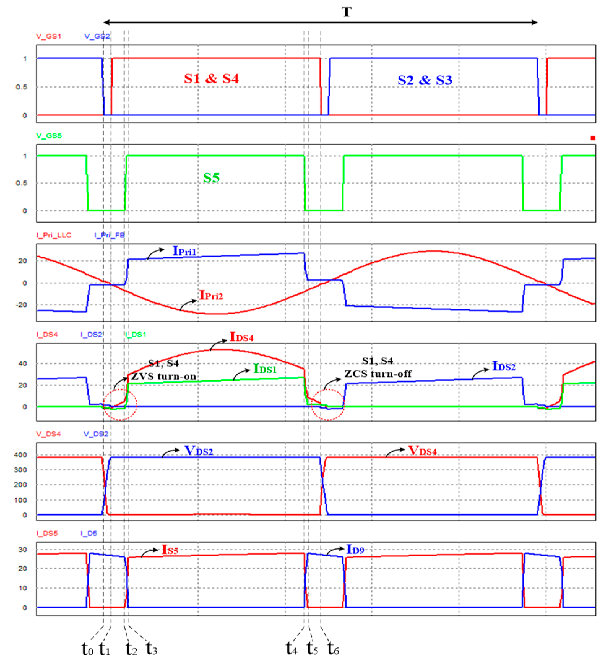
Figure 3 shows the key waveforms of the proposed converter. In the proposed hybrid converter, diagonally opposite switch pair, ( and ) and ( and ), is switched at each time and the secondary side switch is synchronized with the primary switch operation. The primary side switch pair of the proposed circuit operates with a constant duty cycle of 50% at the resonant frequency of the half bridge LLC converter while the secondary switch operates at and its duty cycle is controlled to regulate the output voltage. During the time when the secondary switch is turned off, the primary current is reset, thereby achieving ZVZCS operation for the primary switches.
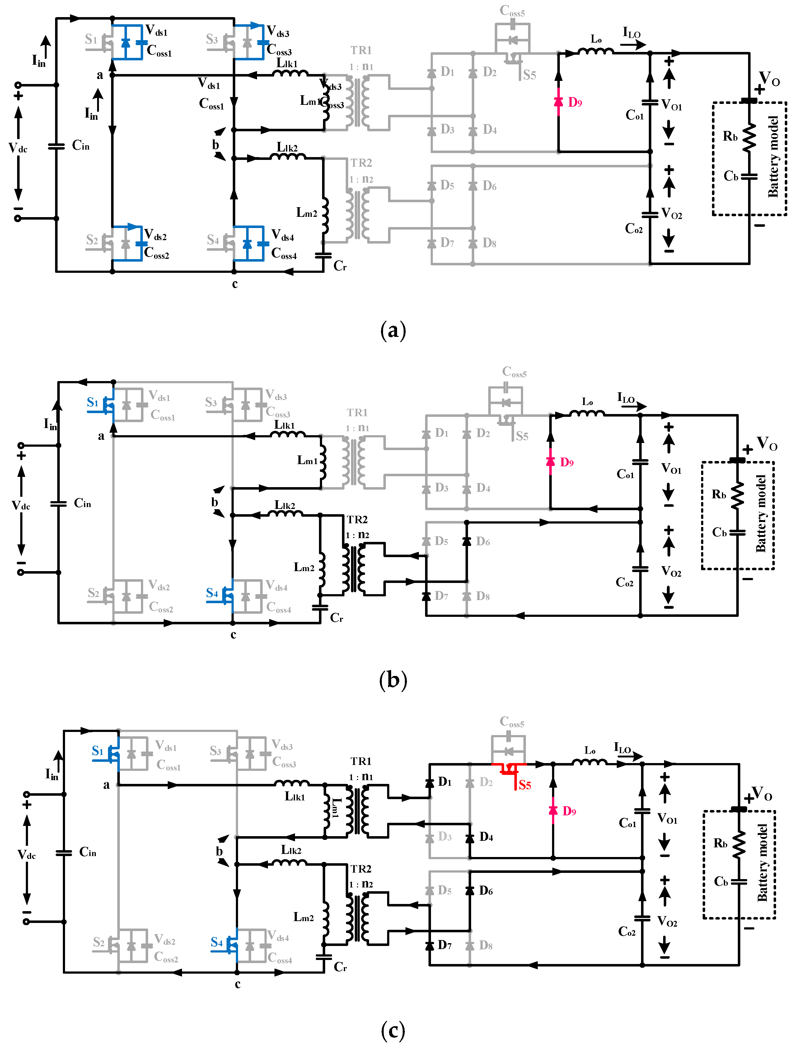
There are six operation modes of the proposed converter in a half switching period as shown in Figure 4. The following assumptions are made for the simplicity of the analysis.
- All of the switching devices are ideal except the output capacitance.
- All of the capacitors, inductors, and transformer are ideal except the leakage inductance of the transformer.
- The output capacitance values of all of the primary switches are the same.
- The leakage inductance values of the transformers are much smaller than the output filter inductances reflected to the primary side. << n2 (where n is the secondary-to-primary-windings-turns ratio).
At , one switch pair ( and is turned off. The primary current of the SSFB transformer charges and , and discharges . At the same time, is discharged by . The primary current of two transformers and the voltages across the four switches are given by:
where ; ; ; .
Since and increase to , and decrease to zero, the intrinsic body diodes of and conduct, thereby achieving ZVS condition for and . In the LLC circuit, is equal to the magnetizing current at and no power is transferred to the secondary side of the LLC converter. During this mode, the output inductor current freewheels.
At , and turn-on with ZVS. However, since is still turned off, only the half bridge LLC converter transfers the power to the load by the resonance between and .
The switch turns on at and the diode is reverse biased. The current at the diode decays to zero and commutes to and , thereby causing a small duty loss. However, it is very small as compared to the conventional PSFB converter.
In this mode, the commutation of the secondary current of the TR1 is completed and the SSFB transfers the power to the load through the switch , , and . The current at the transformer TR1 reaches the reflected current of the output inductor and increases with a slope shown by Equation (7).
The primary current of the LLC converter, , increases with the resonance between the leakage inductor and . It can be represented by the Equation (8).
where and . is the voltage of the resonant capacitor at . Here, the magnetizing current of the transformer TR2, , is a triangular wave with a constant slope represented by the Equation (9).
where is the magnetizing inductance of the transformer TR2. Thus,
where is the initial current flowing through the magnetizing inductance Lm2 at t3.
The LLC converter also transfers the energy to the secondary circuit at the resonant frequency where the voltage gain is unity and independent of the load and the inductance ratio /. Thus, the can be designed large enough, which results in a small magnetizing current of LLC transformer, .
At , is turned off and the voltage across is increased. The diode is forward biased and the current commutation starts to occur from and to . The current resets to almost zero current during this mode. Hence, the circulating current can be eliminated, and hence the loss associated with it. The LLC converter operation remains the same as that in the previous mode.
At , , and are turned off under ZCS condition. The output inductor current freewheels through . The LLC converter operations remains the same as the previous mode.
Since the operation principle of the other half of a switching period is same as the above, it is omitted here.
3. Design Considerations for the Proposed Hybrid Converter
3.1. Voltage Gain
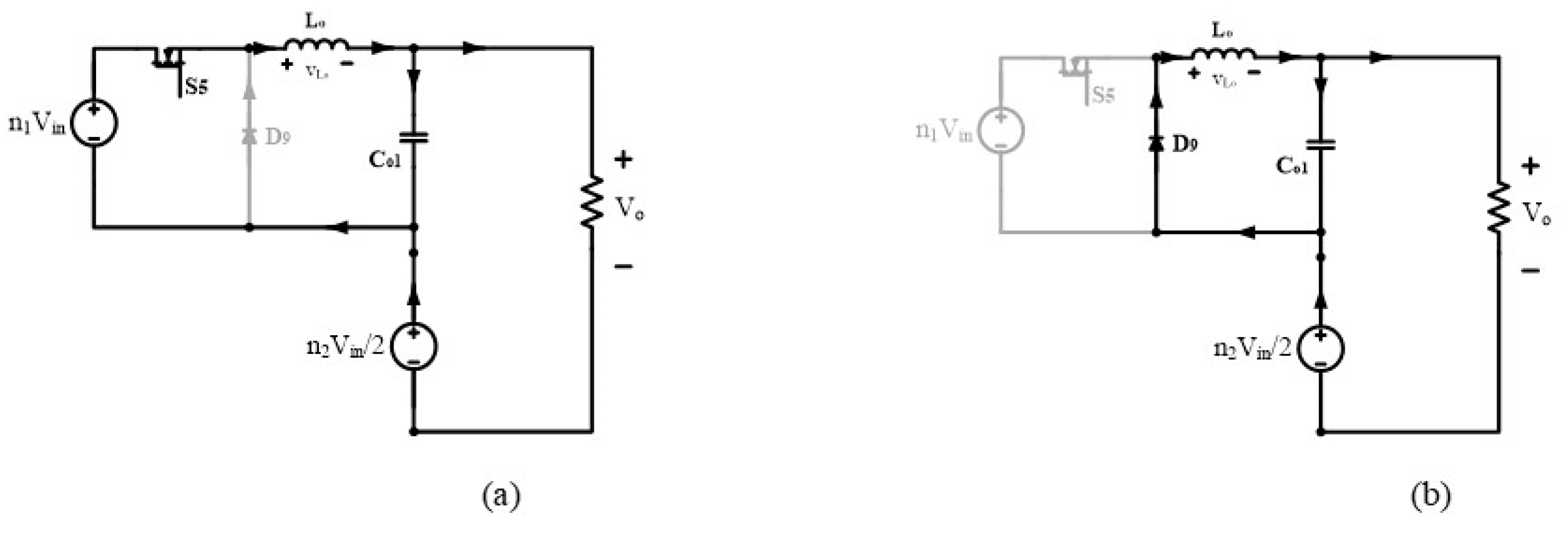
The voltage gain of the proposed converter can be derived based on the equivalent circuit of the proposed SSFB converter at each state as shown in Figure 5. By using the flux balance principle at the output inductor and the closed loop voltage equation at each state the following equation can be obtained.
where is the duty of the switch S5. Therefore, the steady-state voltage gain M of the proposed SSFB converter in the continuous conduction mode can be obtained as follows.
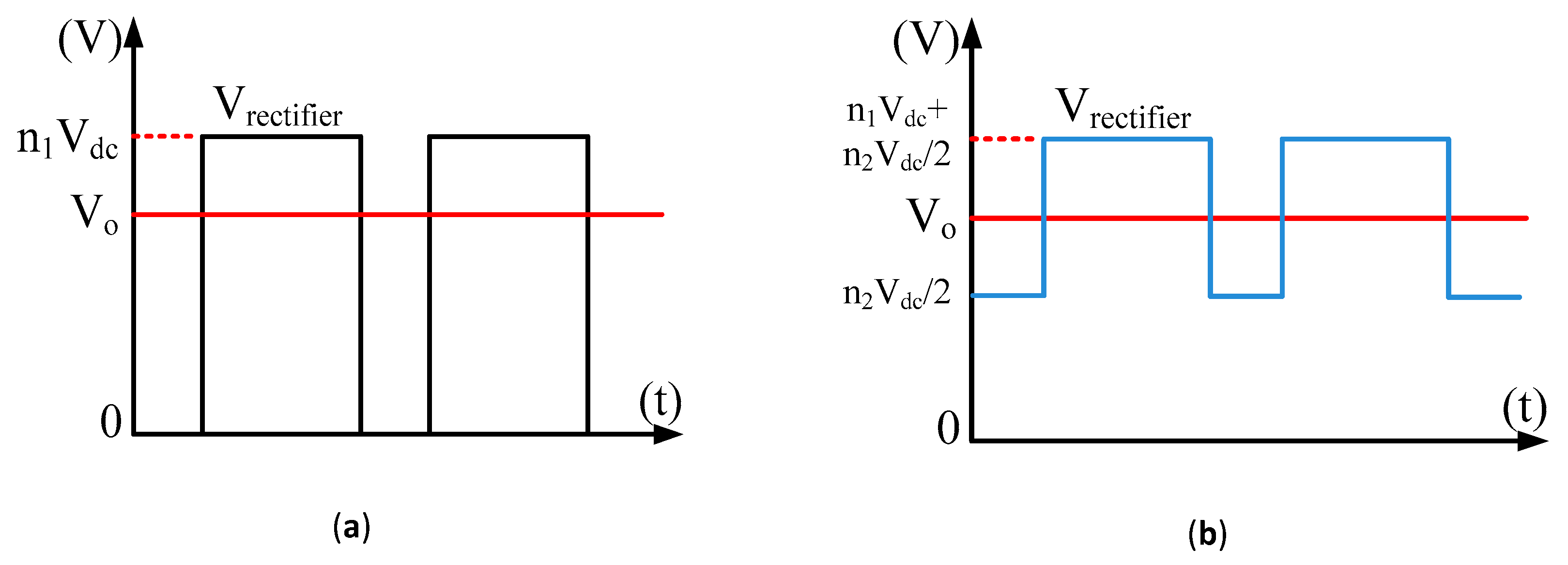
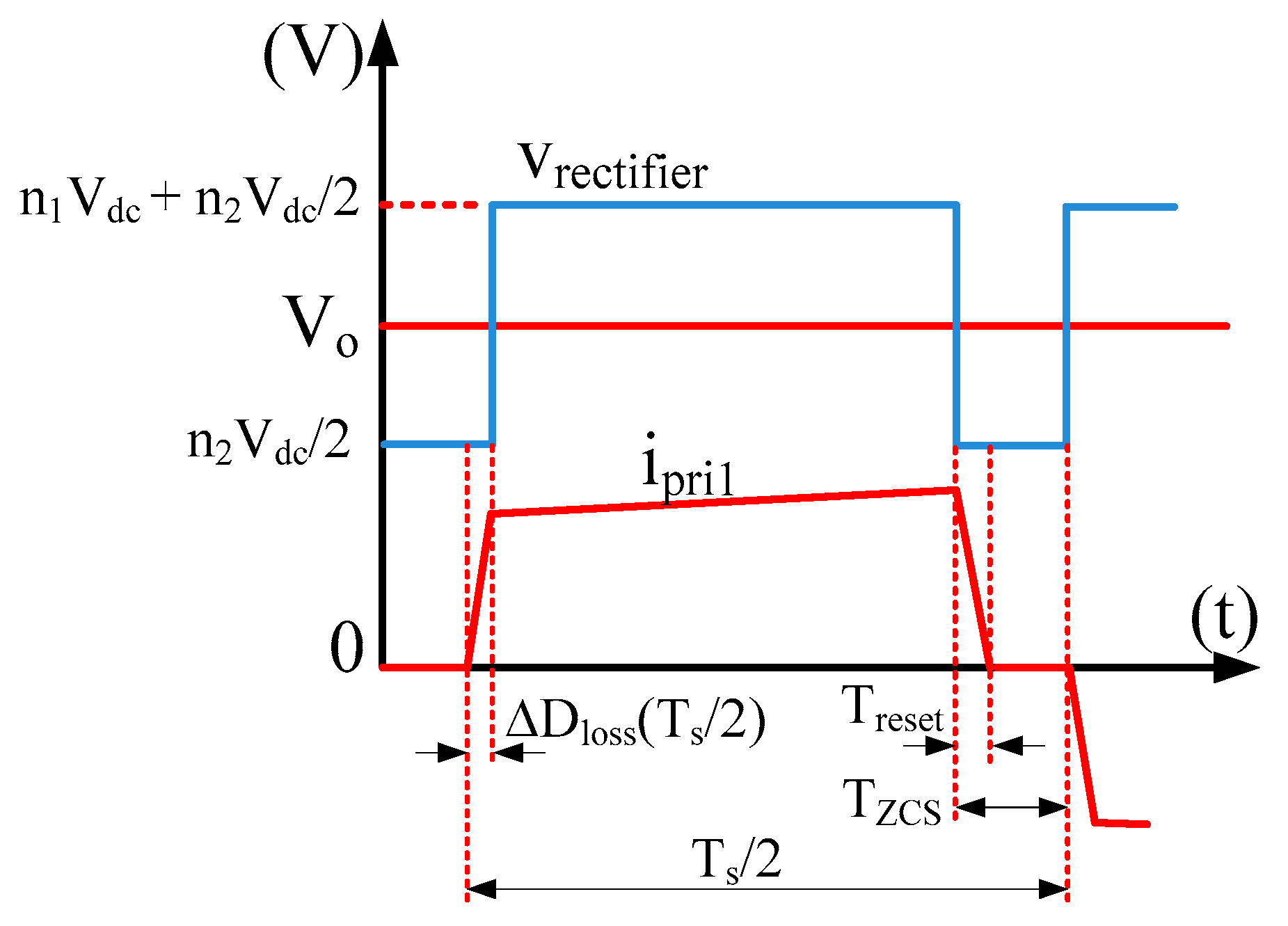
Figure 6 shows the output voltage waveforms of the rectifier in the conventional PSFB converter and the proposed SSFB converter. While the Vrectifier of PSFB becomes zero during the freewheeling time, it is always higher than zero in the proposed SSFB converter. Hence, in the proposed converter it is possible to transfer the power to the output continuously. Since the circulating current does not exist in the proposed SSFB converter there are no power loss and duty loss associated with it.
3.2. Transformer Turns Ratio
The turns-ratio of each transformer can be calculated by the following procedure. As derived earlier in Equation (12) the output voltage of the half bridge LLC converter can be represented by Equation (13).
The output voltage of FB converter can be represented by Equation (14).
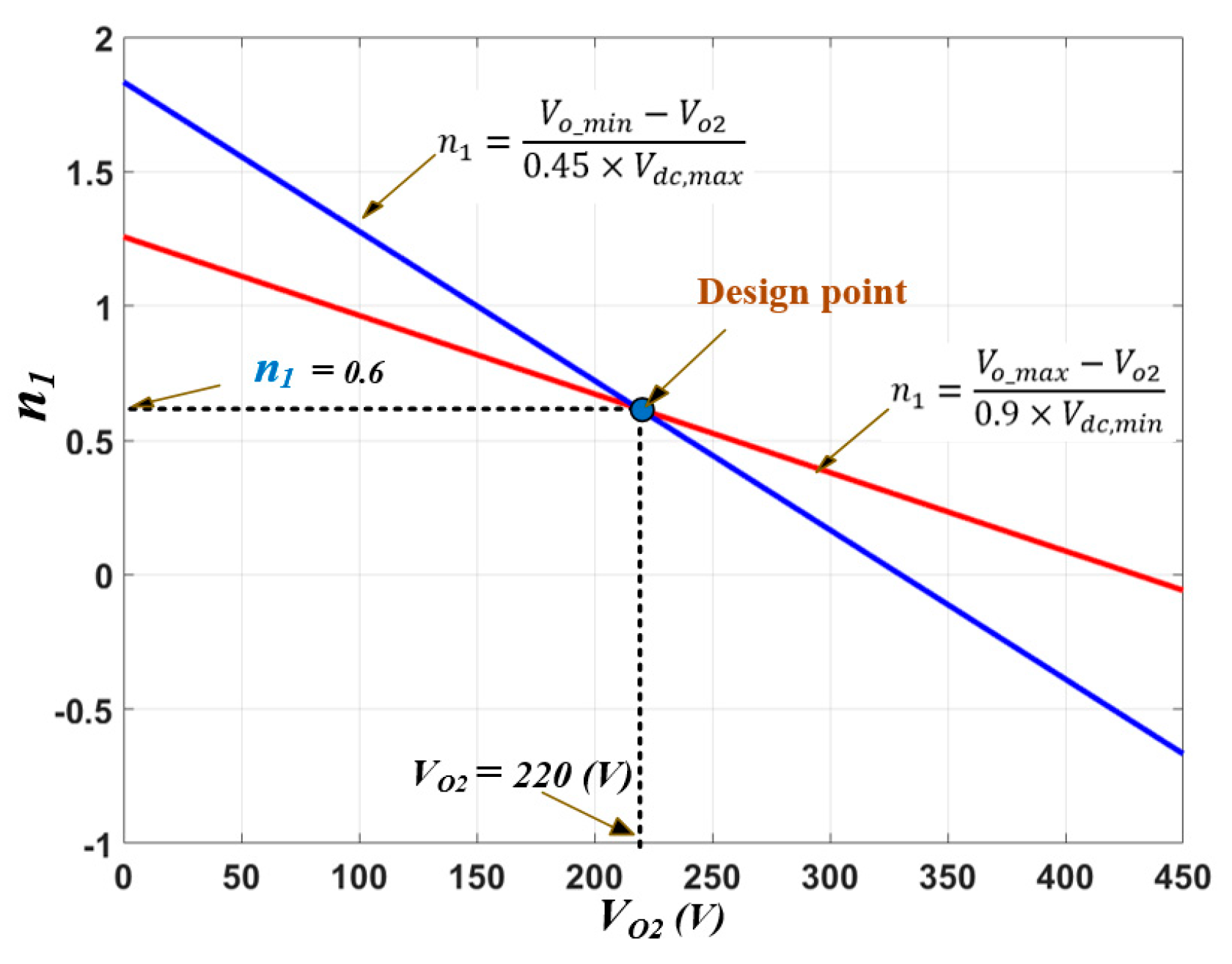
Since the duty of the secondary side switch S5 varies in between , the turns-ratio of the transformer in the full bridge converter can be calculated as follows.
Here, and is the maximum and minimum voltage of the battery pack in the electric vehicle, respectively. The optimal value of can be determined as follows.
From Equation (13), the turns-ratio of the transformer in the half bridge LLC converter can be easily obtained as follows.
3.3. Power Sharing in Between SSFB and LLC Converter
Since the outputs of the proposed hybrid converter are combined in series, the LLC converter transfers the energy to the secondary circuit during the entire switching period. The whole dc output voltage is adjusted by the duty of the secondary side switch of the SSFB converter.
When LLC resonant converter operates at the resonant frequency , the voltage gain is unity and independent of the load condition. The output current of the LLC converter is equal to that of the SSFB converter due to the series connection.
The output voltage based on Equation (12) is:
The ratio of the power assigned for SSFB and LLC converter at a certain output power Po,, can be derived as in Equations (19) and (20).
3.4. ZVS Condition of the Primary Switches
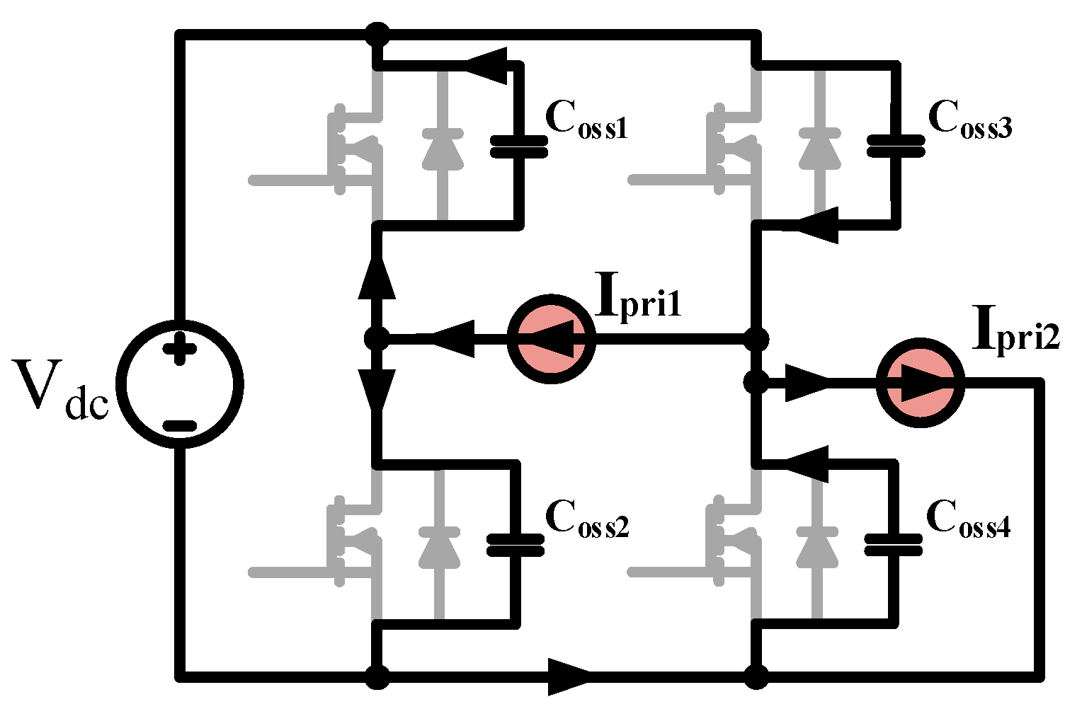
In the proposed hybrid converter, two primary currents in TR1 and TR2 are participating charging and discharging the parasitic output capacitances of the four primary switches. Figure 7 shows the equivalent circuit formed in the mode 1.
In the mode 1 [], is charged and is discharged by ipri1 as shown in Equation (21).
COSS3 is charged and COSS4 is discharged by the sum of ipri1 and ipri2 as shown in Equation (22).
Since Cr >> (Coss3 + Coss4) and Llk + Lm >> Llk, can be treated as a constant current source, respectively.
The peak value of the magnetizing current of TR1 can be represented as follows.
The peak value of the magnetizing current of TR2 can be represented as follows.
In the proposed hybrid SSFB converter the ZVS condition for the primary switches can be achieved all over the load range because the peak values of and are independent of the load as shown in Equations (23) and (24). For the simplicity of the design and need to be designed sufficient to charge three parasitic output capacitors of the primary switches and to discharge one parasitic output capacitor of the primary switch, respectively. Taking it into consideration that is typically less than 5% of a switching period, the magnetizing inductances and should be designed to satisfy the following condition to guarantee ZVS of the primary switches all over the load condition as follows.
3.5. ZCS Condition for the Primary Switches
In the proposed hybrid converter the primary switch pair turns off after the secondary switch turns off. If the primary switch turns off after the secondary switch turns off, the ZCS turn-off condition for the primary switches can be achieved. Hence, the can be reset to zero before the primary switches turn off as shown in Figure 8. The minimum interval to achieve the ZCS condition can be represented by Equation (27).
where is the reflected output current to the primary side of SSFB converter.
3.6. Design of the Output Inductor
The inductor at the output filter can be derived from the rectifier output voltage in Figure 6b.
where is the peak-to-peak value of the current at and is the voltage applied to LO during .
For the proposed converter
For the conventional PSFB converter
In case of EV chargers, the current ripple at LO is worst when the voltage of the battery is lowest, VO = 330 V.
4. Design of the Proposed SSFB Converter for Electric Vehicle Charge Application
In this section the design procedure for the proposed converter is presented. Table 1 shows the specification of the proposed converter for the electric vehicle charge application.
4.1. Turns Ratio of the Transformer
The optimal turns ratio of the transformer in the SSFB converter can be calculated by using Equation (16). Both sides of Equation (16) have been drawn as shown in Figure 9 and the cross point of two lines is the design point. Therefore, the optimal turns ratio of the transformer in the SSFB, , is selected as 0.6 and the output voltage of the LLC converter is 220 V. The turns ratio of the transformer in the HB LLC, , can be easily calculated as 1.12 by using Equation (17).
At nominal output voltage = 400 V, the power of the LLC converter and SSFB converter are calculated simply as follows. , hence
4.2. SSFB Transformer TR1
The magnetizing inductance can be calculated from Equation (25). Given , The core selection for the SSFB transformer can be performed as follows [12]
where is area product of SSFB transformer core (cm4), is core area (cm2), is bobbin winding area (cm2), current density = 400 cir.mils/amp, flux density = 2000 gauss and = 4.5 kW. By using Equation (31), we can calculate = 61.2 cm4.
As mentioned earlier in Section 3.4, zero voltage switching is independent of the value of . Thus, can be designed as small as possible to reduce duty cycle loss and resetting time of the primary current.
The magnetizing inductor has been designed by selecting a gapless high permeability core material. A PQ72/52 is selected and = 64 cm4.
4.3. LLC Transformer TR2
While the parallel type hybrid converter in [25] where TR2 is typically considered as an auxiliary transformer to assist the ZVS of lagging leg switches, the series type hybrid converter requires a large TR2 to handle the current at the lowest output voltage condition. The calculation of LLC transformer can be performed similar to SSFB transformer. However, TR1 and TR2 can be designed with a same size core to enhance the power density [27]. Therefore, the same core PQ72/52 is selected for the transformer TR2.
The magnetizing inductance must meet the Equation (26) to guarantee ZVS at no-load condition. Given , Design of the resonant parameters Llk2 and Cr can be performed based on the ZVS constraint at full-load condition. The reasonable value of the quality factor is selected as 1.3 [28]
The equivalent ac resistance at full load can
At the full load condition of LLC converter = 8.8 Ω. Therefore, = 60.7 μH.
4.4. Resonant Capacitance
Since LLC circuit operates at the resonant frequency , the resonant capacitor can be calculated by using Equation (35).
Therefore, = 0.482 µF
4.5. Output Inductor
From the earlier analysis in Section 3.6, the output inductor value can be obtained by
When = 330 V, = 0.45 and = = is calculated as 679 µH.
5. Experimental Results and Discussions
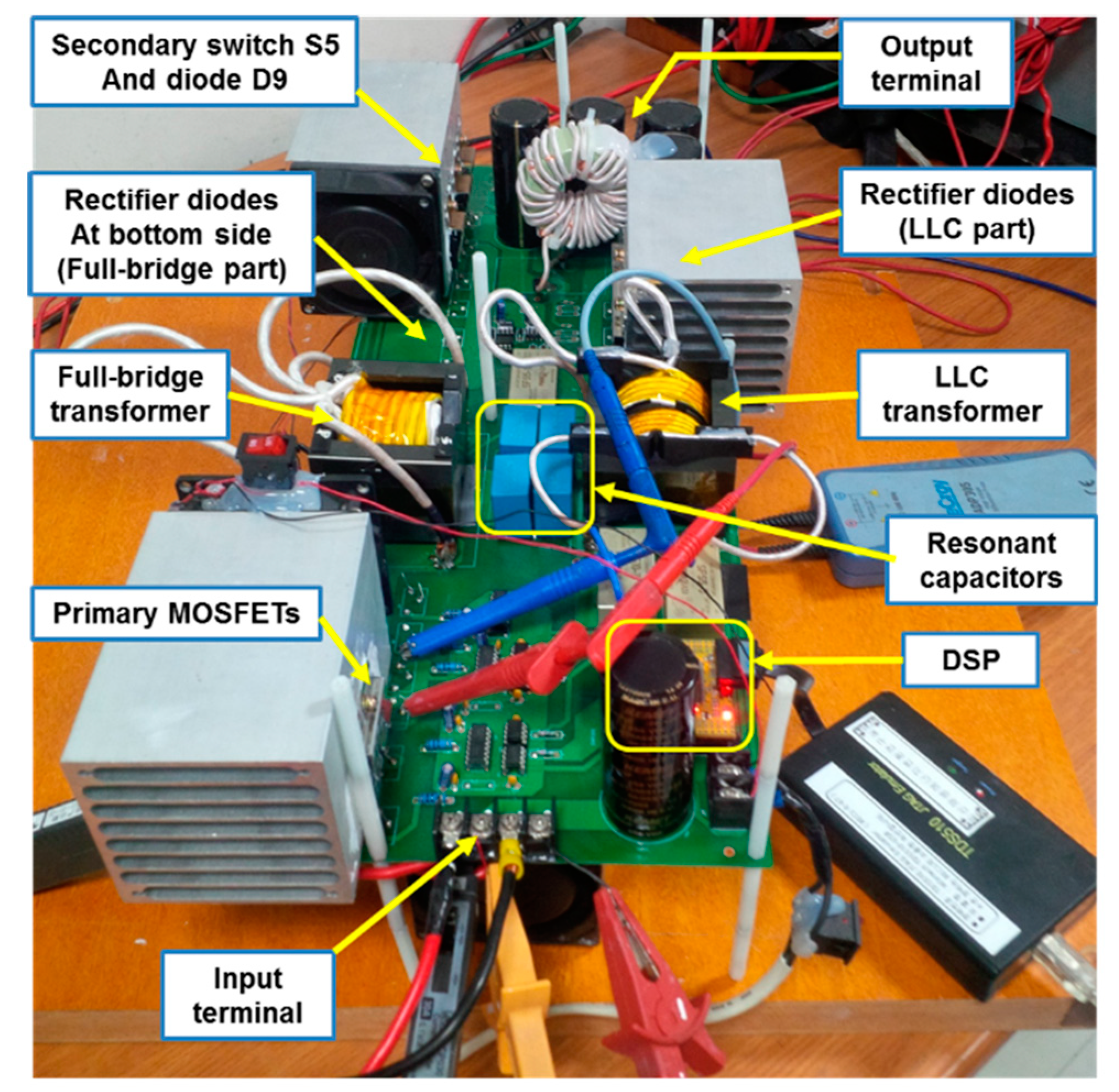
In order to prove the operation principle and the performance of the proposed topology a 10 kW prototype circuit is built as shown in Figure 10. A digital signal processor from Texas Instrument, TMS320F28335, is employed to control the converter and to implement the CC/CV charge algorithm for the EV battery pack.
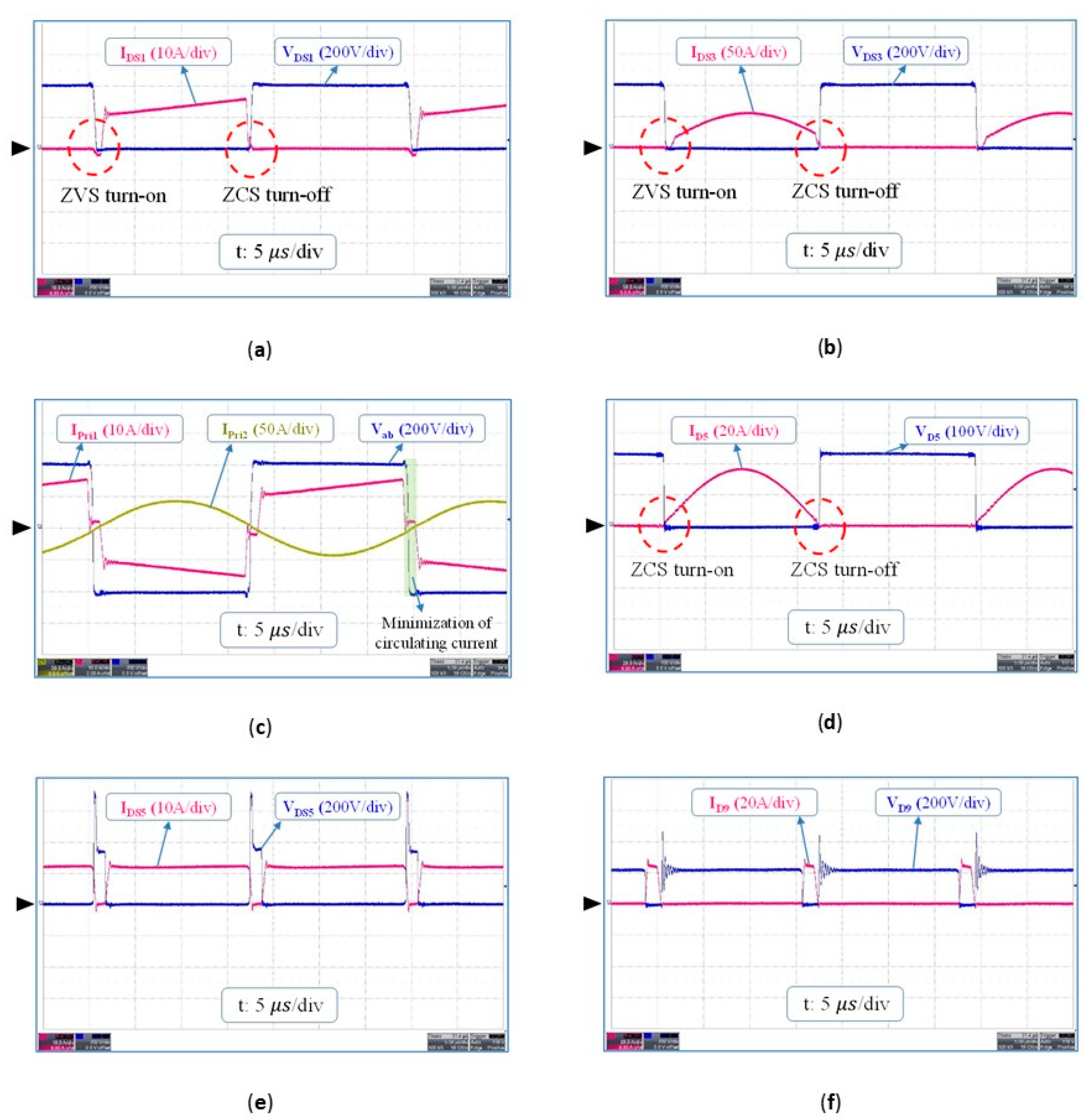
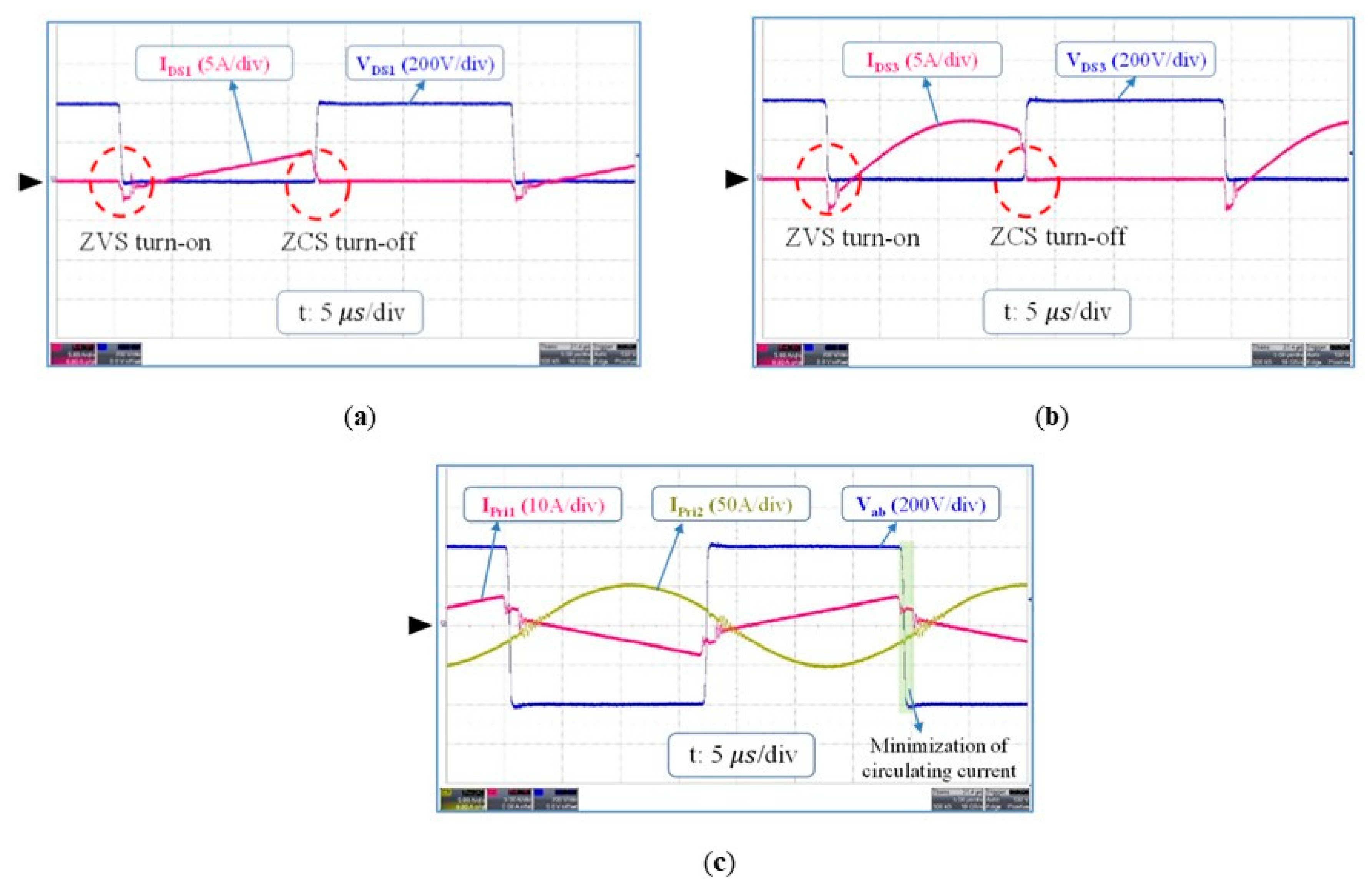
Figure 11a shows the voltage and current waveforms of the leading leg switch of the proposed converter. It is shown that both ZVS turn-on and ZCS turn-off are achieved at this switch. Figure 11b shows the voltage and current of the lagging leg switch . It also shows a complete ZVS turn-on and ZCS turn-off of the lagging leg switch . The current at the switch is the combination of the two converter currents.
Figure 11c shows the primary currents of TR1, , and TR2, . After is turned off, is reset to the magnetizing current, . Therefore, the circulating current in the SSFB converter during the freewheeling period can be minimized, which results in a reduction of the conduction losses. Since the switching frequency is the same as the resonant frequency of the HB LLC converter, waveform is sinusoidal and hence the secondary rectifier diodes of the HB LLC converter in Figure 11d can be turned on and off with ZCS condition. Therefore HB LLC converter transfers the power with minimum losses.
Figure 11e,f show voltage and current of and . Both of them suffer from hard switching. However, since there is no switching loss at the primary side switches and no losses associates with the circulating current in , the saved loss by the proposed converter is much higher than the switching loss at and , resulting in an improvement of overall efficiency.
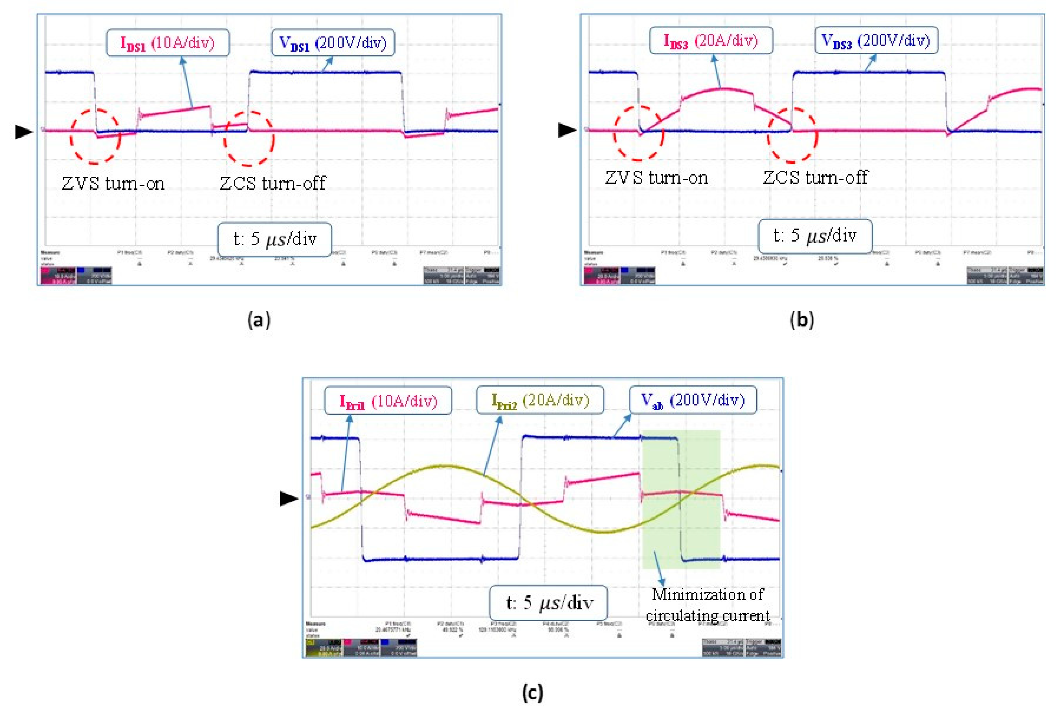
Figure 12 shows the experimental waveforms of the proposed converter at 1 kW. Since the magnetizing current and are sufficient to charge and discharge the output capacitors of the primary switches regardless of the load current, the ZVS turn-on of all the primary switches can be ensured in the light load condition. The ZCS turn-off can be achieved by ensuring the enough delay time as shown in Equation (26).
Figure 13 shows the main waveforms when output voltage is regulated at the minimum value of 330 V. The effective duty of , , is 0.45. It is shown that is maintained at the small magnetizing current which is sufficient to achieve ZVS turn-on condition for the primary side switches during the time between turn-on of a primary switch pair and S5. In addition the circulating current which is a serious problem in the conventional PSFB can be eliminated and the efficiency of the proposed converter can be improved even at low output voltage.
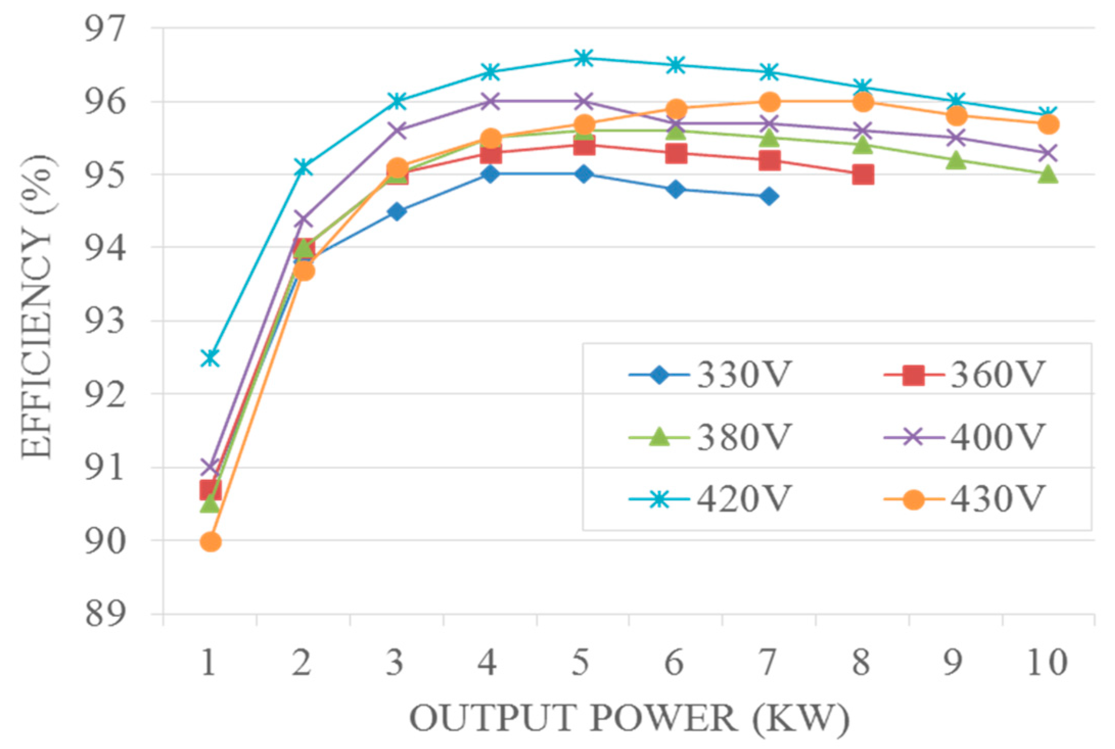
The measured efficiency plots at different load conditions and various output voltages with 400 V nominal input voltage is given in Figure 14. The peak efficiency of the proposed hybrid converter is 96.6% at 5 kW when the output voltage VO is 420 V.
6. Conclusions
In this paper a novel soft-switching hybrid converter combining an SSFB converter and a HB LLC resonant converter is proposed for the On-board charger of EV applications. The experimental results with a 10 kW prototype have been presented to prove the validity and the feasibility of the proposed converter. In the proposed converter since the ZVS operation of the primary switches does not rely on the leakage inductance of the transformer it can be designed as small as possible so that the duty loss can be minimized. With the help of secondary switch the ZCS operation of the primary switches is also possible and there is no circulating current especially at the light load. Therefore it exhibits a high efficiency characteristics over the wide range of load. The smaller size of the passive components in the secondary side and the simple switching scheme can be considered as additional advantages of the proposed converter.
Author Contributions
Author Contributions: D.T. wrote the manuscript and designed the prototype of the proposed converter; M.T. analyzed the proposed converter; W.C. reviewed the manuscript and supervised the research.
Funding
This research was funded by the KEPCO (Korean Electric Power Corporation; Grant number: R17XA05-42).
Acknowledgments
This research was supported by the Korean Electric Power Corporation.
Conflicts of Interest
The authors declare no conflict of interest.
References
- Ehsani, M.; Gao, Y.; Gay, S.E.; Emadi, A. Modern Electric, Hybrid Electric, and Fuel Cell Vehicles, 3rd ed.; CRC Press: Boca Raton, FL, USA, 2018. [Google Scholar]
- Khaligh, A.; Dusmez, S. Comprehensive topological analysis of conductive and inductive charging solutions for plug-in electric vehicles. Trans. Veh. Technol. 2012, 61, 3475–3489. [Google Scholar] [CrossRef]
- Larminie, J.; Lowry, J. Electric Vehicle Technology Explained; Wiley: Hoboken, NJ, USA, 2003. [Google Scholar]
- Saber, A.Y.; Venayagamoorthy, G.K. One million plug-in electric vehicles on the road by 2015. In Proceedings of the 12th International IEEE Conference on Intelligent Transportation Systems, St. Louis, MO, USA, 4–7 October 2009; pp. 1–7. [Google Scholar]
- Level 1 vs Level 2 EV Charging station. Available online: https://www.clippercreek.com/level-1-level-2-charging-station (accessed on 3 July 2019).
- Specifications. Available online: https://www.nissanusa.com/vehicles/electric-cars/leaf/compare-specs (accessed on 3 July 2019).
- On Board Charger. Available online: https://www.tesla.com/support/home-charging-installation/onboard-charger (accessed on 3 July 2019).
- Yilmaz, M.; Krein, P.T. Review of battery charger topologies, charging power levels, and infrastructure for plug-in electric and hybrid vehicles. IEEE Trans. Power Electron. 2013, 28, 2151–2169. [Google Scholar] [CrossRef]
- Pahlevaninezhad, M.; Das, P.; Drobnik, J.; Jain, P.K.; Bakhshai, A.A. Novel ZVZCS full-bridge dc/dc converter used for electric vehicles. IEEE Trans. Ind. Electron. 2012, 27, 2752–2769. [Google Scholar] [CrossRef]
- Gu, B.; Lai, J.; Kees, N.; Zheng, C. Hybrid-Switching Full-Bridge DC–DC Converter with Minimal Voltage Stress of Bridge Rectifier, Reduced Circulating Losses, and Filter Requirement for Electric Vehicle Battery Chargers. IEEE Trans. Power Electron. 2013, 28, 1132–1144. [Google Scholar] [CrossRef]
- Bai, H.; Mi, C.C. Comparison and evaluation of different DC/DC topologies for plug-in hybrid electric vehicle chargers. Int. J. Power Electron. 2012, 4, 119–133. [Google Scholar] [CrossRef]
- Sabate, J.A.; Vlatkovic, V.; Ridley, R.B.; Lee, F.C.; Cho, B.H. Design considerations for high-voltage high-power full-bridge zero-voltage switching PWM converter. In Proceedings of the Applied Power Electronic Electronic Conference, Los Angeles, CA, USA, 11–16 March 1990; pp. 275–284. [Google Scholar]
- Park, K.; Kim, C.; Moon, G.; Youn, M. Voltage Oscillation Reduction Technique for Phase-Shift Full-Bridge Converter. IEEE Trans. Ind. Electron. 2007, 54, 2779–2790. [Google Scholar] [CrossRef]
- Chen, B.; Lai, Y. Switching Control Technique of Phase-Shift-Controlled Full-Bridge Converter to Improve Efficiency Under Light-Load and Standby Conditions Without Additional Auxiliary Components. IEEE Trans. Power Electron. 2010, 25, 1001–1012. [Google Scholar] [CrossRef]
- Koo, G.B.; Moon, G.W.; Youn, M.J. Analysis and design of phase shift full bridge converter with series-connected two transformers. IEEE Trans. Power Electron. 2004, 19, 411–419. [Google Scholar] [CrossRef]
- Gautam, D.; Musavi, F.; Edington, M.; Eberle, W.; Dunford, W.G. An automotive on-board 3.3 kW battery charger for PHEV application. In Proceedings of the IEEE Vehicle Power Propulsion Conference, Chicago, IL, USA, 6–9 September 2011; pp. 1–6. [Google Scholar]
- Jain, P.K.; Kang, W.; Soin, H.; Xi, Y.H. Analysis and design considerations of a load and line independent zero voltage switching full bridge DC/DC converter topology. IEEE Trans. Power Electron. 2002, 17, 649–657. [Google Scholar] [CrossRef]
- Jang, Y.; Jovanovic, M.M.; Chang, Y.M. A new ZVS-PWM full-bridge converter. IEEE Trans. Power Electron. 2003, 18, 1122–1129. [Google Scholar] [CrossRef] [Green Version]
- Wu, X.; Zhang, J.; Xie, X.; Qian, Z. Analysis and Optimal Design Considerations for an Improved Full Bridge ZVS DC–DC Converter with High Efficiency. IEEE Trans. Power Electron. 2006, 21, 1225–1234. [Google Scholar] [CrossRef]
- Chen, W.; Ruan, X.; Zhang, R. A novel zero-voltage-switching PWM full bridge converter. IEEE Trans. Power Electron. 2008, 23, 793–801. [Google Scholar] [CrossRef]
- Koo, G.B.; Moon, G.W.; Youn, M.J. New zero-voltage-switching phase-shift full-bridge converter with low conduction losses. IEEE Trans. Ind. Electron. 2005, 52, 228–235. [Google Scholar] [CrossRef]
- Cho, J.G.; Sabate, J.A.; Hua, G.C.; Lee, F.C. Zero-voltage and zero-current-switching full bridge PWM converter for high-power applications. IEEE Trans. Power Electron. 1996, 11, 622–628. [Google Scholar]
- Lee, I.; Moon, G. Phase-Shifted PWM Converter with a Wide ZVS Range and Reduced Circulating Current. IEEE Trans. Power Electron. 2013, 28, 908–919. [Google Scholar] [CrossRef]
- Lai, J.J.; Miwa, H.; Lai, W.H.; Tseng, N.H.; Lee, C.S.; Lin, C.H.; Shih, Y.W. A high-efficiency on-board charger utilitzing a hybrid LLC and phase-shift DC–DC converter. In Proceedings of the International Conference on Intelligent Green Building and Smart Grid (IGBSG), Taipei, Taiwan, 23–25 April 2014; pp. 1–8. [Google Scholar]
- Lee, I.; Moon, G. Half-Bridge Integrated ZVS Full-Bridge Converter with Reduced Conduction Loss for Electric Vehicle Battery Chargers. IEEE Trans. Ind. Electron. 2014, 61, 3978–3988. [Google Scholar] [CrossRef]
- Gu, B.; Lin, C.; Chen, B.; Dominic, J.; Lai, J. Zero-Voltage-Switching PWM Resonant Full-Bridge Converter with Minimized Circulating Losses and Minimal Voltage Stresses of Bridge Rectifiers for Electric Vehicle Battery Chargers. IEEE Trans. Power Electron. 2013, 28, 4657–4667. [Google Scholar] [CrossRef]
- Liu, C.; Gu, B.; Lai, J.S.; Wang, M.Y.; Ji, Y.C.; Cai, G.W.; Zhao, Z.; Chen, C.L.; Zheng, C.; Sun, P.W. High-Efficiency Hybrid Full-Bridge–Half-Bridge Converter with Shared ZVS Lagging Leg and Dual Outputs in Series. IEEE Trans. Power Electron. 2013, 28, 849–861. [Google Scholar] [CrossRef]
- Lee, I.O. A Hybrid PWM-Resonant DC–DC Converter for Electric Vehicle Battery Charger Applications. J. Power Electron. 2015, 15, 1158–1167. [Google Scholar] [CrossRef]
- Tran, D.D.; Vu, H.N.; Lee, H.H.; Pham, V.L.; Choi, W. A novel 10kW hybrid converter for the electric vehicle charge applications. In Proceedings of the 2016 IEEE Transportation Electrification Conference and Expo, Asia-Pacific (ITEC Asia-Pacific), Busan, Korea, 1–4 June 2016; pp. 220–224. [Google Scholar]
Figure 1.
Different types of hybrid converter. (a) Series type [24]; (b) [24] paralleled type; (c) FB converter integrated with a symmetric half-bridge converter connected in parallel [25]; (d) hybrid PWM and resonant converter with shared lagging-leg switches [26]; (e) hybrid PWM and resonant converter with dual outputs connected in series [27]; (f) half-bridge LLC SRC integrated into a PSFB converter [28].

Figure 2.
Proposed hybrid dc–dc converter for the on-board charger.

Figure 3.
Key waveforms of the proposed converter.

Figure 4.
Operation modes of the proposed converter (a) [t0~t1], (b) [t1~t2], (c) [t2~t3], (d) [t3~t4], (e) [t4~t5], and (f) [t5~t6].
Figure 4.
Operation modes of the proposed converter (a) [t0~t1], (b) [t1~t2], (c) [t2~t3], (d) [t3~t4], (e) [t4~t5], and (f) [t5~t6].


Figure 5.
Equivalent circuit of the proposed soft switching full bridge (SSFB) converter (a) S5 on-time interval (b) S5 off-time interval.
Figure 5.
Equivalent circuit of the proposed soft switching full bridge (SSFB) converter (a) S5 on-time interval (b) S5 off-time interval.

Figure 6.
Voltage waveform of the rectifier. (a) Conventional full-bridge converter, (b) proposed SSFB converter.
Figure 6.
Voltage waveform of the rectifier. (a) Conventional full-bridge converter, (b) proposed SSFB converter.

Figure 7.
Equivalent circuit of the proposed hybrid converter during mode 1.

Figure 8.
Minimum interval to achieve zero current switching (ZCS) condition for the primary switches.
Figure 8.
Minimum interval to achieve zero current switching (ZCS) condition for the primary switches.

Figure 9.
Optimal design point of SSFB transformer turn ratio.

Figure 10.
Prototype of the proposed 10 kW On-board charger.

Figure 11.
Experimental waveforms of the proposed converter at 10 kW. (a,b) Voltage and current waveforms of the primary switch and , respectively (c) primary current waveform of the transformer in the SSFB converter and the HB LLC converter, respectively and the primary side voltage (d–f) voltage and current waveforms of secondary rectifier diode , secondary side switch , and freewheeling diode .

Figure 12.
Experiment waveforms at 1 kW (10% of load). (a,b) Voltage and current of the primary switch and , respectively (c). Primary current of TR1, and primary voltage of TR1, of SSFB transformer and primary current of TR2,
Figure 12.
Experiment waveforms at 1 kW (10% of load). (a,b) Voltage and current of the primary switch and , respectively (c). Primary current of TR1, and primary voltage of TR1, of SSFB transformer and primary current of TR2,

Figure 13.
Experiment waveforms at the minimum output voltage 330 V (a,b) Voltage and current of the primary switch and , respectively. (c) Primary current of TR1, and primary voltage of TR1, of SSFB transformer and primary current of TR2,.
Figure 13.
Experiment waveforms at the minimum output voltage 330 V (a,b) Voltage and current of the primary switch and , respectively. (c) Primary current of TR1, and primary voltage of TR1, of SSFB transformer and primary current of TR2,.

Figure 14.
Measured efficiency plots of the proposed hybrid converter.


Table 1.
Design specification of the proposed converter.
| Parameter | Designator | Value |
|---|---|---|
| Input Voltage Range | 380–400 [V] | |
| Input Voltage Nominal | 390 [V] | |
| Output Voltage Range | 330–430 [V] | |
| Output Voltage Nominal | 400 [V] | |
| Maximum Output Power | 10 [kW] | |
| Switching frequency | 29.4 [kHz] |
Table 2.
Key parameters of the design and implementation.
| Parameter | Calculated Value | Measured Value |
|---|---|---|
| Turn ratio of the TR1 (n11 : n12) | 11 : 7 | 11 : 7 |
| Leakage inductance of the TR1 () | 12.4 [µH] | |
| Magnetizing inductance of the TR1 () | [mH] | 1.5 [mH] |
| Turn ratio of the TR2 (n21 : n22) | 14 : 16 | 14 : 16 |
| Leakage inductance of the TR2 () | 60.7 [µH] | 65 [µH] |
| Magnetizing inductance of the TR2 () | [mH] | 800 [µH] |
| Resonant capacitor () | 0.482 [ | 0.45 [ |
| Output inductor of SSFB converter () | 679 [µH] | 685 [µH] |
Table 3.
Components used in the prototype converter.
| Component | Manufacture | Part# |
|---|---|---|
| Primary side MOSFETs | Fairchild | FCH76N60N |
| Secondary side MOSFETs | IXYZ | IXFB110N60P3 |
| Diode Rectifiers | IR | 60APU06 |
| Resonant Film Capacitors | EPCOS | B32912B3334M |
| Magnetic Ferrite Core of Transformer | Changsung | PQ7252 |
© 2019 by the authors. Licensee MDPI, Basel, Switzerland. This article is an open access article distributed under the terms and conditions of the Creative Commons Attribution (CC BY) license (http://creativecommons.org/licenses/by/4.0/).
Share and Cite
MDPI and ACS Style
Tran, D.-D.; Tran, M.-T.; Choi, W. A Hybrid Soft Switching Full Bridge Converter Suitable for the Electric Vehicle Charge Applications. Energies 2019, 12, 2707. https://doi.org/10.3390/en12142707
AMA Style
Tran D-D, Tran M-T, Choi W. A Hybrid Soft Switching Full Bridge Converter Suitable for the Electric Vehicle Charge Applications. Energies. 2019; 12(14):2707. https://doi.org/10.3390/en12142707
Chicago/Turabian StyleTran, Dai-Duong, Manh-Tuan Tran, and Woojin Choi. 2019. "A Hybrid Soft Switching Full Bridge Converter Suitable for the Electric Vehicle Charge Applications" Energies 12, no. 14: 2707. https://doi.org/10.3390/en12142707
Note that from the first issue of 2016, this journal uses article numbers instead of page numbers. See further details here.