A Feasibility Study of Fabrication of Piezoelectric Energy Harvesters on Commercially Available Aluminum Foil


School of Electrical Engineering, Korea Advanced Institute of Science and Technology, 291 Daehak-ro, Yuseong-gu, Daejeon 34141, Korea
*
Author to whom correspondence should be addressed.
Energies 2019, 12(14), 2797; https://doi.org/10.3390/en12142797
Submission received: 26 June 2019
/
Revised: 14 July 2019
/
Accepted: 17 July 2019
/
Published: 20 July 2019
(This article belongs to the Special Issue Piezoelectric Materials)
Abstract
:In this paper, we present zinc oxide (ZnO)-based flexible harvesting devices employing commercially available, cost-effective thin aluminum (Al) foils as substrates and conductive bottom electrodes. From the device fabrication point of view, Al-foils have a relatively high melting point, allowing for device processing and annealing treatments at elevated temperatures, which flexible plastic substrate materials cannot sustain because of their relatively low melting temperatures. Moreover, Al-foil is a highly cost-effective, commercially available material. In this work, we fabricated and characterized various kinds of multilayered thin-film energy harvesting devices, employing Al-foils in order to verify their device performance. The fabricated devices exhibited peak-to-peak output voltages ranging from 0.025 V to 0.140 V. These results suggest that it is feasible to employ Al-foils to fabricate energy-efficient energy harvesting devices at relatively high temperatures. It is anticipated that with further process optimization and device integration, device performance can be further improved.
1. Introduction
With much progress in a variety of small-scale sensors, various energy harvesting technologies have also been developed. Zinc oxide (ZnO), in particular, having a large piezoelectric constant has drawn much attention, since it can be deposited in the form of high-quality thin films [1]. Further, lead-free ZnO is a nontoxic, environmentally friendly, and biocompatible material [2], thus, it can be used to enable piezoelectric energy harvesters that are implanted into the body or in contact with the body skin. Unlike most ferroelectric materials, it has the advantage that ZnO does not need any poling process after depositing the ZnO thin film [3,4,5,6]. However, lead-free ZnO-based piezoelectric energy harvesters produce lower output voltages than lead zirconate titanate (PZT)-based harvesters, containing toxic piezoelectric materials [7]. Many research results have reported on various piezoelectric energy harvesters using polyethylene naphthalate (PEN), polyethylene terephthalate (PET), various metal wires, various flexible substrates, etc., in order to enhance the output voltages [8,9,10,11,12,13,14,15,16]. Also, various piezoelectric energy harvesters have been fabricated which exploit insulators to inhibit the so-called screening effect of free carriers, compensating for the positively polarized parts of ZnO, thus reducing the piezoelectric effect [7,8,11,13,14]. To suppress the screening effect, wide-band-gap or p-type semiconductor materials have been combined with ZnO [7,8,11,12,15,16,17]. Moreover, mathematical analysis and simulation studies have been theoretically performed to evaluate and interpret the piezoelectric characteristics or phenomenon of piezoelectric materials and devices [18,19].
Some researchers have developed piezoelectric energy harvesters using polyimide (PI) flexible substrates or stainless steel (STS) substrates in an effort to ensure that the substrate will endure any heat processing treatments implemented at temperatures above 400 °C, because plastic substrates become unstable during the annealing process, even below this temperature [20,21]. We have also tried to find a way of annealing devices at relatively high temperatures with the hope of enhancing device performance. Considering candidate substrates, we have chosen to use an aluminum (Al) foil which is highly cost-effective, commercially available, and easy to use. There has been an attempt to make a ZnO/Al stacked structure by depositing a ZnO film on an Al-foil by the sol-gel method, focusing on the photocatalytic effect [22] instead of observing its piezoelectric effect. In this work, we fabricate piezoelectric energy harvesters by depositing ZnO films on Al-foils in order to observe their piezoelectric energy harvesting performance. The Al-foil was cut into a certain size, on which various thin films were deposited, which enabled post-annealing up to ~500 °C (a temperature which PEN substrates cannot withstand), leading to device healing [23,24]. This device annealing treatment may lead to an output voltage improvement and a film durability enhancement, simultaneously.
In this work, to further improve Al-foil-based energy harvesters, we deposited chromium (Cr) as an interlayer to enhance the adhesion between the two adjoined film layers in the device. Other researchers have used chromium (Cr) as a metal electrode [10,25] as well as a thin film layer [26,27] to improve the adhesion quality. Considering these advantages, we deposited a Cr interlayer below the zinc oxide (ZnO) thin film and above the indium tin oxide (ITO) bottom electrode.
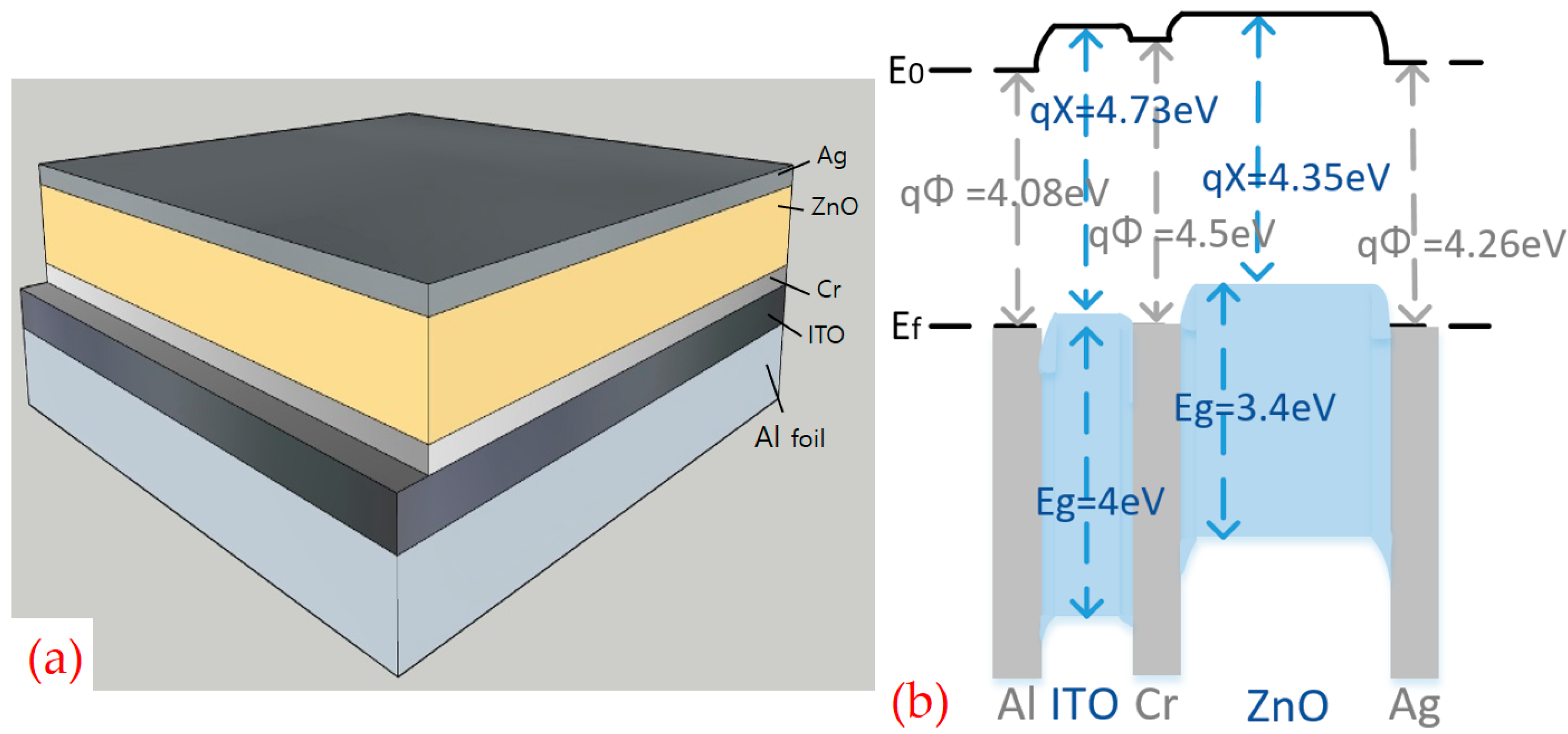
We also fabricated various energy harvesters using an aluminum nitride (AlN), n-type a-Si, and SiO2 layer beneath or on the Cr layer which were used in our earlier studies to form a potential energy barrier. Finally, to simplify the device structure and processing steps, and lower the cost, we fabricated and characterized the energy harvesters (stacked with Ag/ZnO/Cr/Al layers) without the ITO bottom electrode by depositing only the Cr and ZnO films on the Al-foil. These simplified devices have been demonstrated to function well through performance tests, indicating that the newly adopted Al-foils in this work could act as a substrate and bottom electrode, potentially replacing conventional ITO/PEN substrates. Figure 1a shows the device structure of the five-layered films (Al, ITO, Cr, ZnO, Ag) stacked on top of each other and the corresponding energy band diagram (Figure 1b). The work functions (qΦ) of Al, Cr, Ag are, respectively, 4.08 eV, 4.5 eV, 4.26 eV [12,28,29]. And ITO has a bandgap (Eg) of 4 eV and an electron affinity (qΧ) of 4.73 eV [30,31]. On the other hand, ZnO has a bandgap of 3.4 eV and an electron affinity of 4.35 eV [12].
2. Materials and Methods
In this work, 18 μm-thick aluminum foil (Samjin foil, Daegu, Korea) was used as a substrate material to fabricate various energy harvesters. The Al-foil sheet is low-cost, commercially available, and frequently used for cooking, wrapping, crafting, and packaging purposes. A single sheet of Al-foil was cut into pieces each 2.5 × 2 cm2 in size. The Al-foils substrates were dipped in hydrofluoric (HF) acid (H2O:HF = 51:49) (J.T.BakerTM, Center Valley, PA, USA) for 10 min to eliminate native oxide [32], followed by rinsing three times with deionized (DI) water, drying with a nitrogen blow gun and a halogen lamp. All thin films were deposited by a radio frequency (RF) magnetron sputtering system (HVS-340, Hanvac, Daejeon, Korea). The process details of each film deposition are summarized in Table 1. Prior to each film deposition, all targets were presputtered for 20 min under the same conditions (RF power of 150 W, working pressure of 1 × 10⁻² Torr, Ar gas flow rate of 20 sccm), to remove undesirable residues and contaminants. An ITO (4N, iTASCO) target was sputtered with an RF power of 200 W for 30 min to form a Schottky barrier bottom electrode [16]. A ZnO (5N, iTASCO) target was sputtered with an RF power of 200 W for 90 min. A Cr (4N, iTASCO) target was sputtered with an RF power of 160 W for 30 min to improve the adhesion between both ZnO and ITO films.
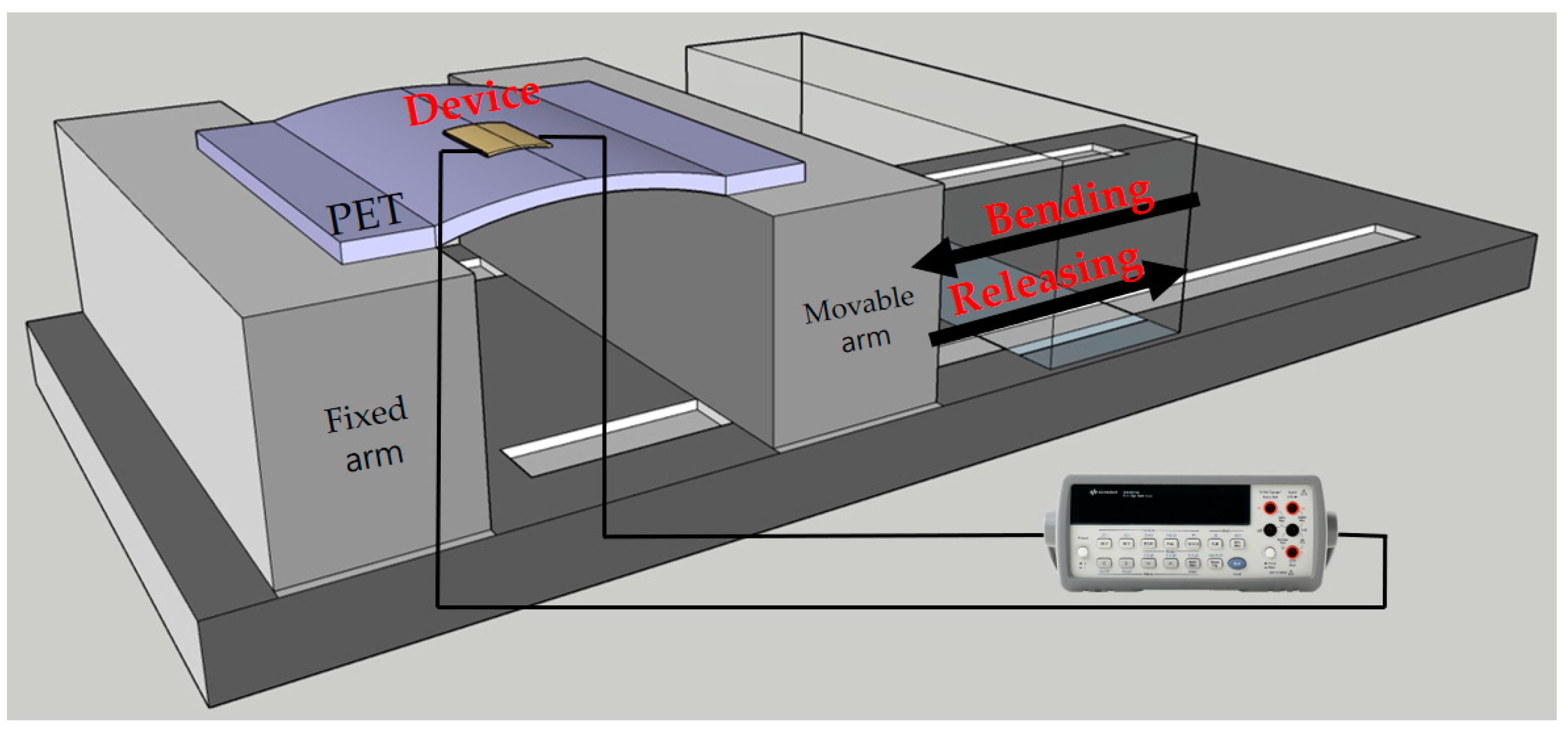
All the fabricated samples were loaded into an electric furnace (Daesung Electric, Pocheon, Korea) and annealed for a fixed length of time in an Ar atmosphere. The formation of the top electrode using Ag paste (CANS, ELCOAT P-100, Jinchemical, Busan, Korea) completed the device fabrication. The measurement of device output voltages was conducted using a bending machine (Labtech Science, Daejeon, Korea), to which a sheet of resilient PET was attached as a bending platform for the device to be measured. All output voltages were measured with a digital multimeter (34401A, Keysight Technologies, Santa Rosa, CA, USA) while bending with 0.2519% strain, at a 0.17%s−1 strain rate, as shown in Figure 2. Many experiments were carried out to attach the Al-foil-based devices to the PET bending platform efficiently by using adhesives, cyanoacrylate, electric iron, and double-sided tape.
The deposition conditions of all the materials used in this work are described in detail, as summarized in Table 1. It is noted that all the films were deposited under the working pressure of 1 × 10⁻² Torr, while the target-to-substrate distance was 12 cm, and the substrate rotation speed was 8 rpm.
For the ZnO deposition in particular, a mixture of 18 sccm Ar and 12 sccm N2O gas was flowing during the sputtering process to reduce the free-carrier concentration in the ZnO film, leading directly to the improvement of device performance [16].
Many previously reported devices fabricated on flexible plastic substrates [10,12,13,14,16,17] have an intrinsic limitation to increasing process temperatures. Thus, in this work, instead of flexible plastic substrates, we have attempted to employ the Al-foil as a substrate to further increase the process temperatures, which helpfully allows for annealing heat treatments at higher temperatures.
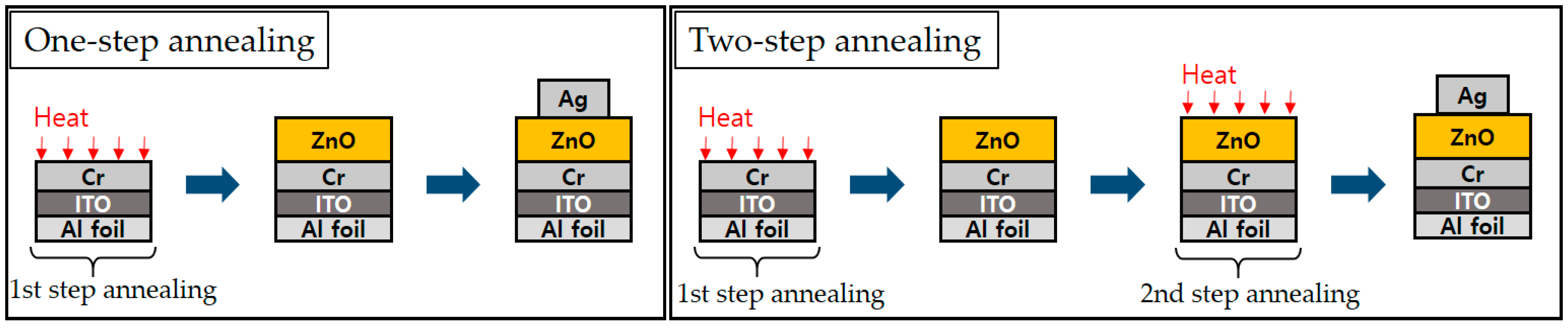
As illustrated in Figure 3, to understand the effect of annealing on device performance, some devices were annealed once before ZnO deposition (one-step annealing) or twice immediately before and after ZnO deposition (two-step annealing), while others were not annealed at all (nonannealing or as-deposited). The formation of the top electrode using Ag paste completed the device fabrication.
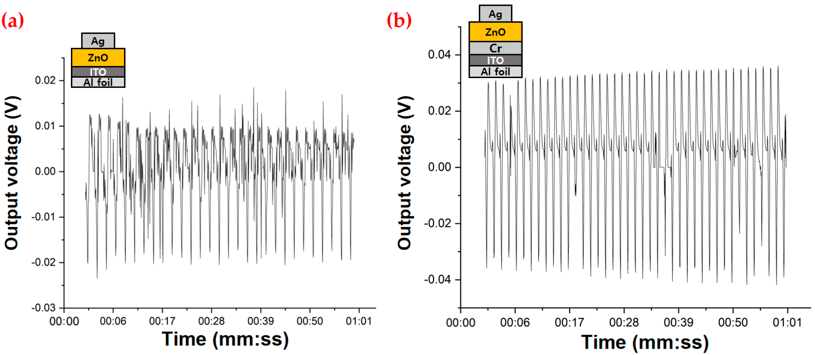
We have confirmed the feasibility of using Al-foil sheet as a substrate on which we fabricated several Ag/ZnO/ITO/Al-foil structured devices by depositing both ZnO and ITO films under various process conditions. However, the output voltages of these devices were not stably generated or as high as expected, possibly because of wrinkling or cracking of the stacked films. To resolve this issue, a thin layer of Cr was deposited to enhance the adhesion between the ZnO and ITO films [26,27], and Ag/ZnO/Cr/ITO/Al-foil structured devices were also fabricated. The surface morphologies of the two different structures, those with and without the Cr layer, after a bending test were investigated using a microscope (S39A, Microscopes Inc., Saint Louis, MO, USA). The devices including the Cr layer showed better output voltages (Figure 4), apparently due to a significant reduction in the wrinkling or cracking phenomenon of the stacked films, as shown in the micrographs of Figure 5.
The output voltages for all devices were measured and compared, as shown in Figure 6, Figure 7, Figure 8 and Figure 9. Interestingly, in this work, it was found that the one-step annealing resulted in better performance than the two-step annealing, however, the reason remains unclear and requires a further study.
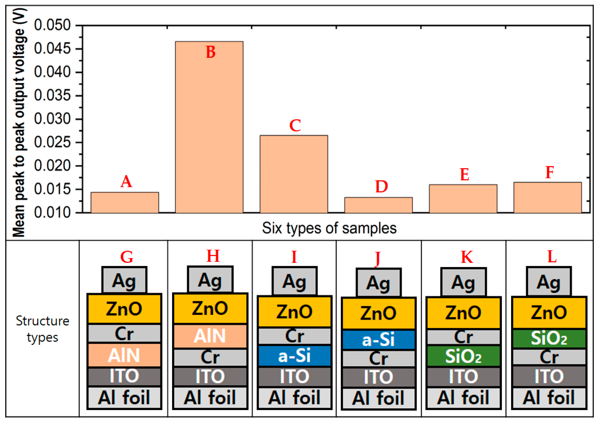
To further verify the feasibility of using the Al-foil as a substrate for the fabrication of energy harvesters, we fabricated modified devices by sputtering AlN (5N, iTASCO), n-type a-Si (5N, iTASCO), or SiO2 (4N, iTASCO) targets and depositing interlayers between the ZnO and Cr films, or Cr and ITO films, to form a total of six different device structures. These devices were measured and compared, as shown in Figure 10. The device with the stacked layers of Ag/ZnO/AlN/Cr/ITO/Al-foil showed higher output voltages than the other devices.
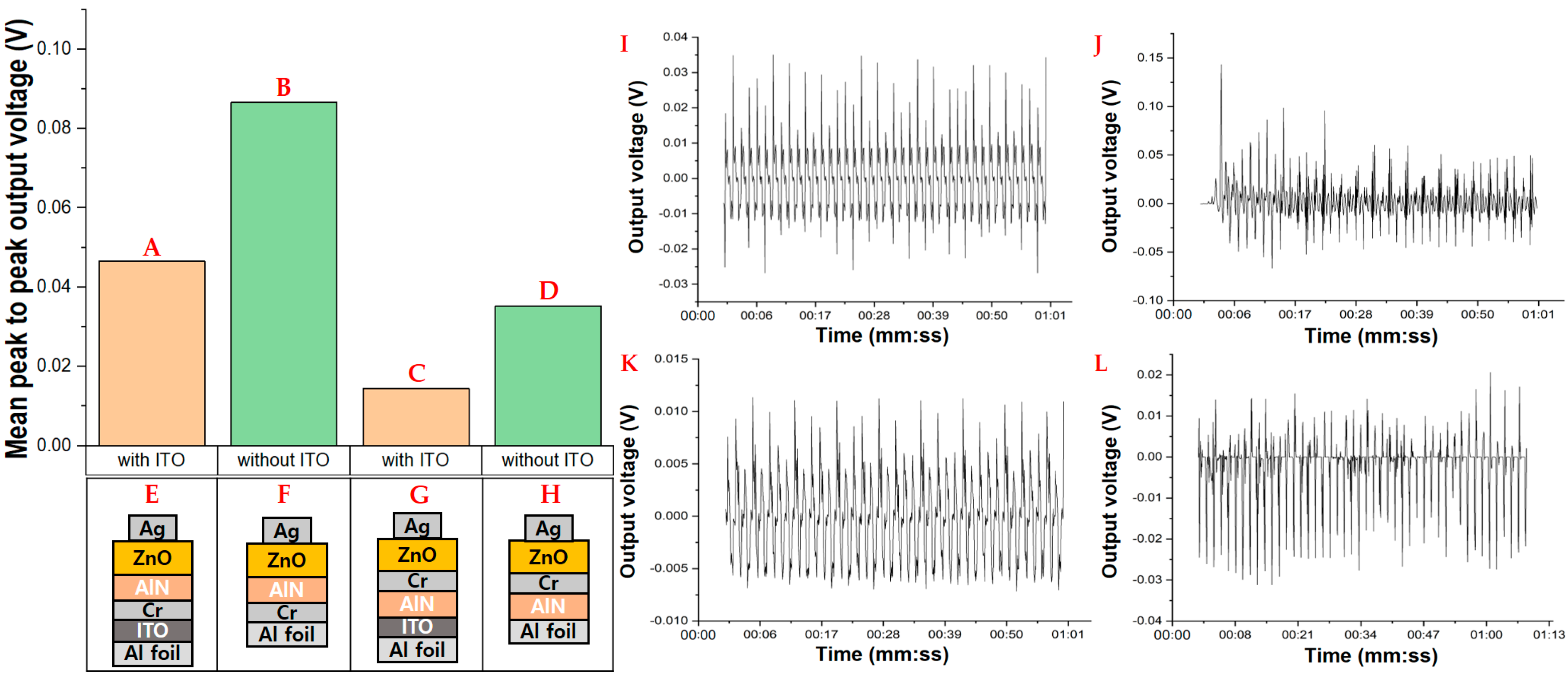
In this work, to fabricate the devices in a more cost-effective way, we replaced the ITO bottom electrode with Al-foil because the Al-foil is a conductive material, acting as a substrate as well as an electrode. From this standpoint, we have fabricated four different device structures on Al-foil by substituting the conventional ITO electrode with the Al-foil electrode. Measurements of their respective output voltages (as mean peak-to-peak output voltage histograms) were conducted for comparison. The fabricated devices and their measured output voltages are shown in Figure 11.
3. Results and Discussion
In this work, the piezoelectric devices fabricated on Al-foil substrates generate substantial output voltages. As shown in Figure 4, we fabricated and measured two sample devices, with and without a Cr layer. The output voltages of (a) Ag/ZnO/ITO/Al-foil and (b) Ag/ZnO/Cr/ITO/Al-foil structured devices are compared. The addition of a Cr layer resulted in a more stable output waveform and larger peak-to-peak voltage, increased from approximately 0.035 V to 0.070 V, while the device without a Cr layer was found to have a less stable waveform with a smaller mean peak-to-peak voltage of 0.035 V. We have investigated and compared the microscopic surface morphologies of both (a) ZnO/ITO/Al-foil and (b) ZnO/Cr/ITO/Al-foil by optical microscopy, after completion of 20 bending cycles (bending was performed prior to the formation of the Ag top electrode), as shown in Figure 5. Each sample shows significantly different morphologies in the magnified micrographs (×400). More crack propagation seems to occur in the stacked film structure without a Cr layer. By depositing a thin Cr interlayer, the adhesion between the ITO and ZnO layers is apparently improved, leading to an enhancement of the device output voltage.
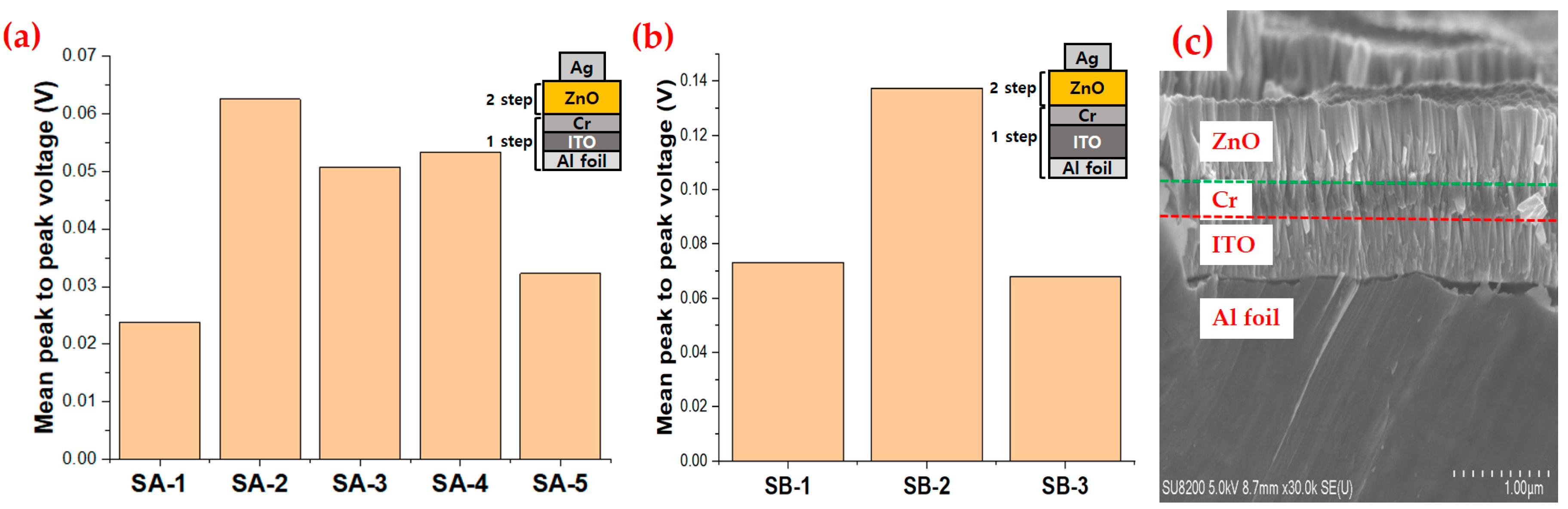
As shown in Figure 6, for further understanding of annealing effects, the six fabricated devices were annealed using either the one-step or two-step annealing processes described in Figure 3. The detailed annealing conditions and sample names are summarized in Table 2. The samples which were annealed at 300 °C for 1 h in the “one-step annealing” showed significantly better output voltages than the other devices. The output voltages of the eight samples included in Figure 6 are compared, as shown in Figure 7.
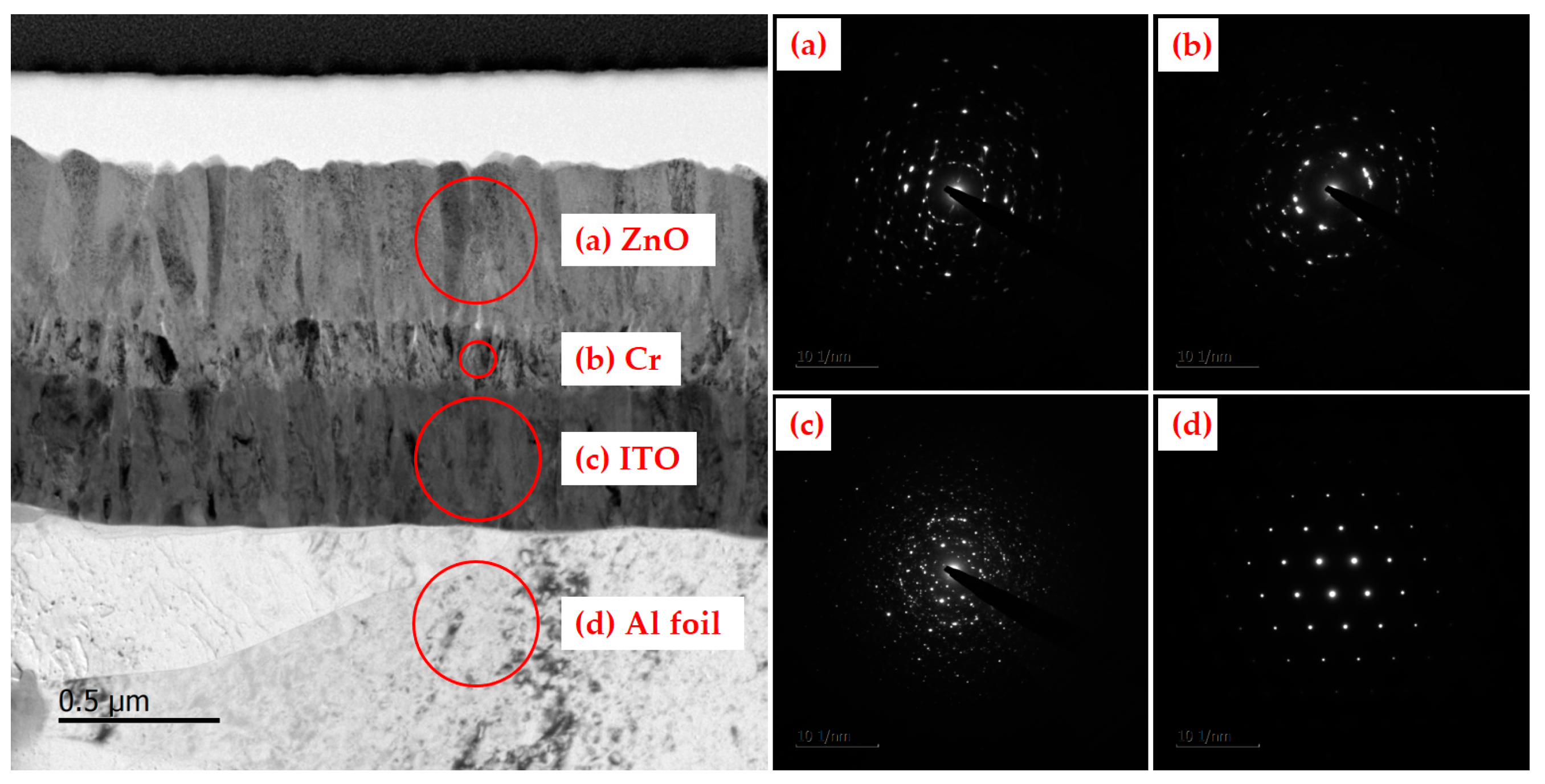
To analyze the crystallinity and composition of the deposited material, the ZnO/Cr/ITO/Al-foil samples were prepared by focused ion beam (FIB). As shown in Figure 8, a low-resolution transmission electron microscope (LRTEM) cross-sectional image of the sample was measured, and the selected area electron diffraction (SAED) patterns of each layer were also acquired by 200 KeV LRTEM. The SAED patterns of the four layers are labeled, respectively, from (a) to (d). All the layer materials appear to exist in polycrystalline forms, where the Al-foil has a face-centered cubic structure [33].
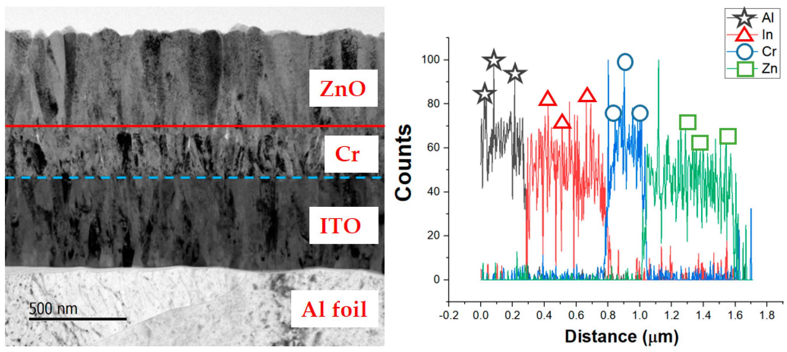
Energy-dispersive X-ray spectroscopy (EDS) depth profiling was performed, as shown in Figure 9. Compositional analysis confirmed the constituent materials of each layer in the ZnO/Cr/ITO/Al-foil structure.
Similarly to other reports [12,13,14], we fabricated additional devices including each material (AlN, SiO2, or a-Si) used in our earlier researches for a further study, as shown in Figure 10. Here, each target of AlN (5N, iTASCO), n-type a-Si (5N, iTASCO), or SiO2 (4N, iTASCO) were used to fabricate the devices shown in Figure 10. The deposition conditions along with film thicknesses are described in Table 1. The output voltages were extracted from the fabricated devices, and are compared in Figure 10. In particular, the sample B of the Ag/ZnO/AlN/Cr/ITO/Al-foil structure showed the highest output voltage.
To design the energy harvesting devices in a more cost-effective way, we have fabricated various kinds of similarly formed devices with and without an ITO layer on the Al-foil substrate.
As shown in Figure 11, the devices without an ITO layer have shown more than a two-fold increase in output voltage over those with an ITO layer. It is speculated that with the elimination of the ITO layer, the energy barrier at the Cr/ITO interface may not exist, thus making it easier for the electrons to flow toward the top electrode, as shown in Figure 1b.
Overall, the Al-foil substrate-based devices have shown relatively low output voltages when measured after 180 bending cycles. The exact mechanism of device operation has not been clearly explained yet, however, we attribute the relatively low performance to the bending-cycle-induced strain, causing an interface adhesion deterioration, finally leading to possible wrinkling, delamination, or even cracking of the stacked film layers.
4. Conclusions
We have fabricated and characterized various piezoelectric energy harvesting devices employing a commercially available Al-foil. The adoption of a thin Cr film as an interlayer may enhance the adhesion between two layers (ZnO and ITO), reducing the formation and/or propagation of cracks in devices during bending cycle tests, and thus improving the output voltage stability. Moreover, the annealing effects on the device output voltage performance were investigated under various annealing conditions. In addition to the annealing conditions, the existence of the ITO bottom electrode layer was found to significantly affect the device performance. Overall, the fabricated devices have shown peak-to-peak output voltages ranging from 0.025 V to 0.140 V. The devices without the ITO electrode layer showed two-fold higher output voltages than those with the ITO electrode layer. These findings suggest that it may be possible to employ various kinds of commercially available, cost-effective Al-foils to fabricate more energy-efficient energy harvesting devices, requiring further integration and optimization of device fabrication processes. This work could contribute to developing more advanced energy harvesting devices adopting Al-foil substrates.
Author Contributions
Conceptualization, methodology, validation, formal analysis, investigation, resources, data curation, writing original draft preparation, visualization, C.Y.; equipment preparation and management, B.J.; supervision, project administration, G.Y.
Funding
This research was supported by Basic Science Research Program through the National Research Foundation of Korea (NRF) funded by the Ministry of Education (Grant No. 2016R1D1A1B01007074).
Conflicts of Interest
The authors declare no conflict of interest.
References
- Olutade, B.; Hunt, W. Sensitivity analysis of a thin film bulk acoustic resonator ladder filter. In Proceedings of the International Frequency Control Symposium, Orlando, FL, USA, 30 May 1997. [Google Scholar]
- Wang, Z.L. Piezoelectric Nanogenerators Based on Zinc Oxide Nanowire Arrays. Science 2006, 312, 242–246. [Google Scholar] [CrossRef] [PubMed]
- Xu, Q.Y.; Wang, Y.; Wang, Y.G.; Du, X.L.; Xue, Q.K.; Zhang, Z. Polarity determination of ZnO thin films by electron holography. Appl. Phys. Lett. 2004, 84, 2067–2069. [Google Scholar] [CrossRef] [Green Version]
- Corso, A.D.; Posternak, M.; Resta, R.; Baldereschi, A. Ab initio study of piezoelectricity and spontaneous polarization in ZnO. Phys. Rev. B 1994, 50, 10715–10721. [Google Scholar] [CrossRef] [PubMed]
- Gopal, P.; Spaldin, N. Polarization, Piezoelectric Constants, and Elastic Constants of ZnO, MgO, and CdO. J. Electron. Mater. 2006, 35, 538–542. [Google Scholar] [CrossRef]
- Dahiya, R.; Valle, M. Robotic Tactile Sensing, Technologies and System; Springer: Berlin/Heidelberg, Germany, 2013. [Google Scholar]
- Yin, B.; Qiu, Y.; Zhang, H.; Lei, J.; Chang, Y.; Ji, J.; Luo, Y.; Zhao, Y.; Hu, L. Piezoelectric performance enhancement of ZnO flexible nanogenerator by a NiO–ZnO p–n junction formation. Nano Energy 2015, 14, 95–101. [Google Scholar] [CrossRef]
- Lei, J.; Yin, B.; Qiu, Y.; Zhang, H.; Chang, Y.; Luo, Y.; Zhao, Y.; Ji, J.; Hu, L. Flexible piezoelectric nanogenerator based on Cu2O–ZnO p–n junction for energy harvesting. RSC Adv. 2015, 5, 59458–59462. [Google Scholar] [CrossRef]
- Yang, R.; Qin, Y.; Dai, L.; Wang, Z.L. Power generation with laterally packaged piezoelectric fine wires. Nat. Nanotechnol. 2008, 4, 34–39. [Google Scholar] [CrossRef]
- Lee, M.; Chen, C.Y.; Wang, S.; Cha, S.N.; Park, Y.J.; Kim, J.M.; Chou, L.J.; Wang, Z.L. Correction: A Hybrid Piezoelectric Structure for Wearable Nanogenerators. Adv. Mater. 2012, 24, 5283. [Google Scholar] [CrossRef]
- Przezdziecka, E.; Chusnutdinow, S.; Guziewicz, E.; Snigurenko, D.; Stachowicz, M.; Kopalko, K.; Reszka, A.; Kozanecki, A. The p-ZnO:N/i-Al2O3/n-GaN heterostructure—Electron beam induced profiling, electrical properties and UV detectivity. J. Phys. D Appl. Phys. 2015, 48, 325105. [Google Scholar] [CrossRef]
- Lee, E.; Park, J.; Yim, M.; Kim, Y.; Yoon, G. Characteristics of piezoelectric ZnO/AlN−stacked flexible nanogenerators for energy harvesting applications. Appl. Phys. Lett. 2015, 106, 023901. [Google Scholar] [CrossRef]
- Yoon, C.; Jeon, B.; Yoon, G. Formation and Characterization of Various ZnO/SiO2-Stacked Layers for Flexible Micro-Energy Harvesting Devices. Appl. Sci. 2018, 8, 1127. [Google Scholar] [CrossRef]
- Jeon, B.; Ha, J.; Yoon, C.; Yoon, G. Effect of a-Si thin film on the performance of a-Si/ZnO-stacked piezoelectric energy harvesters. Appl. Phys. Lett. 2018, 113, 243902. [Google Scholar] [CrossRef]
- Park, H.K.; Lee, K.Y.; Seo, J.S.; Jeong, J.A.; Kim, H.K.; Choi, D.; Kim, S.W. Charge-Generating Mode Control in High-Performance Transparent Flexible Piezoelectric Nanogenerators. Adv. Funct. Mater. 2011, 21, 1187–1193. [Google Scholar] [CrossRef]
- Lee, E.; Park, J.; Yim, M.; Jeong, S.; Yoon, G. High-efficiency micro-energy generation based on free-carrier-modulated ZnO:N piezoelectric thin films. Appl. Phys. Lett. 2014, 104, 213908. [Google Scholar] [CrossRef]
- Lee, K.Y.; Kumar, B.; Seo, J.S.; Kim, K.H.; Sohn, J.I.; Cha, S.N.; Choi, D.; Wang, Z.L.; Kim, S.W. P-Type Polymer-Hybridized High-Performance Piezoelectric Nanogenerators. Nano Lett. 2012, 12, 1959–1964. [Google Scholar] [CrossRef]
- Dannier, A.; Brando, G.; Ruggiero, F.N. The Piezoelectric Phenomenon in Energy Harvesting Scenarios: A Theoretical Study of Viable Applications in Unbalanced Rotor Systems. Energies 2019, 12, 708. [Google Scholar] [CrossRef]
- Craciun, E.; Baesu, E.; Soos, E. General solution in terms of complex potentials for incremental antiplane states in prestressed and prepolarized piezoelectric crystals: Application to Mode III fracture propagation. J. Appl. Math. 2005, 70, 39–52. [Google Scholar] [CrossRef]
- Singkaselit, K.; Sakulkalavek, A.; Sakdanuphab, R. Effects of annealing temperature on the structural, mechanical and electrical properties of flexible bismuth telluride thin films prepared by high-pressure RF magnetron sputtering. Adv. Nat. Sci. Nanosci. Nanotechnol. 2017, 8, 035002. [Google Scholar] [CrossRef] [Green Version]
- Kim, M.; Kim, K. Rapid thermal annealing at the temperature of 650 °C Ag films on SiO2 deposited STS substrates. Appl. Sci. Converg. Technol. 2017, 26, 208–213. [Google Scholar]
- Peng, F.; Wang, H.; Yu, H.; Chen, S. Preparation of aluminum foil-supported nano-sized ZnO thin films and its photocatalytic degradation to phenol under visible light irradiation. Mater. Res. Bull. 2006, 41, 2123–2129. [Google Scholar] [CrossRef]
- Kim, D.H.; Yim, M.; Chai, D.; Yoon, G. Improvements of resonance characteristics due to thermal annealing of Bragg reflectors in ZnO-based FBAR devices. Electron. Lett. 2003, 39, 962–964. [Google Scholar] [CrossRef]
- Lee, E.; Mai, L.; Yoon, G. Development of High-Quality FBAR Devices for Wireless Applications Employing Two-Step Annealing Treatments. IEEE Microw. Wirel. Compon. Lett. 2011, 21, 604–606. [Google Scholar] [CrossRef]
- Isarakorn, D.; Sambri, A.; Janphuang, P.; Briand, D.; Gariglio, S.; Triscone, J.M.; Guy, F.; Reiner, J.W.; Ahn, C.H.; Rooij, N.F.D. Epitaxial piezoelectric MEMS on silicon. J. Micromech. Microeng. 2010, 20, 055008. [Google Scholar] [CrossRef]
- Todeschini, M.; Fanta, A.B.D.S.; Jensen, F.; Wagner, J.B.; Han, A. Influence of Ti and Cr Adhesion Layers on Ultrathin Au Films. ACS Appl. Mater. Interfaces 2017, 9, 37374–37385. [Google Scholar] [CrossRef] [Green Version]
- Mai, L.; Lee, J.Y.; Pham, V.S.; Yoon, G. Design and Fabrication of ZnO-Based FBAR Microwave Devices for Mobile WiMAX Applications. IEEE Microw. Wirel. Compon. Lett. 2007, 17, 867–869. [Google Scholar] [CrossRef]
- Eastment, R.M.; Mee, C.H.B. Work function measurements on (100), (110) and (111) surfaces of aluminium. J. Phys. F: Met. Phys. 1973, 3, 1738–1745. [Google Scholar] [CrossRef]
- Attema, J.J.; Uijttewaal, M.A.; Wijs, G.A.D.; Groot, R.A.D. Work function anisotropy and surface stability of half-metallic CrO2. Phys. Rev. B 2008, 77, 165109. [Google Scholar] [CrossRef]
- Kim, H.; Gilmore, C.M.; Piqué, A.; Horwitz, J.S.; Mattoussi, H.; Murata, H.; Kafafi, Z.H.; Chrisey, D.B. Electrical, optical, and structural properties of indium–tin–oxide thin films for organic light-emitting devices. J. Appl. Phys. 1999, 86, 6451–6461. [Google Scholar] [CrossRef]
- Pethuraja, G.G.; Welser, R.E.; Sood, A.K.; Lee, C.; Alexander, N.J.; Efstathiadis, H.; Haldar, P.; Harvey, J.L. Current-Voltage Characteristics of ITO/p-Si and ITO/n-Si Contact Interfaces. Adv. Mater. Phys. Chem. 2012, 02, 59–62. [Google Scholar] [CrossRef] [Green Version]
- Firek, P.; Szmidt, J.; Nowakowska-Langier, K.; Zdunek, K. Electric Characterization and Selective Etching of Aluminum Oxide. Plasma Process. Polym. 2009, 6, 840–843. [Google Scholar] [CrossRef]
- Ren, N.; Zhu, J.; Ban, S. Highly transparent conductive ITO/Ag/ITO trilayer films deposited by RF sputtering at room temperature. AIP Adv. 2017, 7, 055009. [Google Scholar] [CrossRef] [Green Version]
Figure 1.
Design of a typical energy harvester in this work: (a) schematic of the Ag/ZnO/Cr/ITO/Al-foil stacked structure, and (b) the corresponding energy band diagram at equilibrium state.
Figure 1.
Design of a typical energy harvester in this work: (a) schematic of the Ag/ZnO/Cr/ITO/Al-foil stacked structure, and (b) the corresponding energy band diagram at equilibrium state.

Figure 2.
Schematic of the bending machine used to measure the output voltages in this work which is connected to a Keysight Technologies 34401A.
Figure 2.
Schematic of the bending machine used to measure the output voltages in this work which is connected to a Keysight Technologies 34401A.

Figure 3.
Schematics of the one-step and two-step annealing processes defined in this work.

Figure 4.
Examples of raw output voltages of (a) Ag/ZnO/ITO/Al-foil and (b) Ag/ZnO/Cr/ITO/Al-foil structured devices. Here, the device with a thin Cr layer exhibits a significantly more stable output waveform and increased peak-to-peak voltage than the device without the Cr layer.
Figure 4.
Examples of raw output voltages of (a) Ag/ZnO/ITO/Al-foil and (b) Ag/ZnO/Cr/ITO/Al-foil structured devices. Here, the device with a thin Cr layer exhibits a significantly more stable output waveform and increased peak-to-peak voltage than the device without the Cr layer.

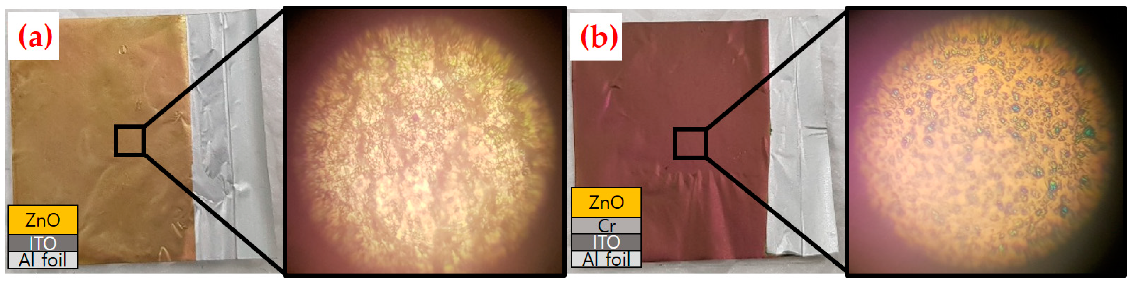
Figure 5.
Comparison of optical micrographs of (a) ZnO/ITO/Al-foil and (b) ZnO/Cr/ITO/Al-foil structures after 20 bending cycles (sample bending was performed prior to the formation of the Ag top electrode). Each sample shows significantly different morphologies in the magnified micrographs (×400). More crack propagation seems to occur in the stacked film structure without a Cr layer.

Figure 6.
The eight devices were formed on the Al-foil substrates. Each device was annealed under different conditions, as specified in Table 2. (a) The five samples of the Ag/ZnO/Cr/ITO structure (SA-1 to SA-5) were formed on Al-foil substrates with an ITO layer thickness of 446 nm. (b) The other three samples (SB-1 to SB-3) were formed on the same Al-foil substrates with an ITO layer thickness of 1390 nm. (c) A representative SEM cross-section image of the sample SA-1 (scale bar 1 μm).

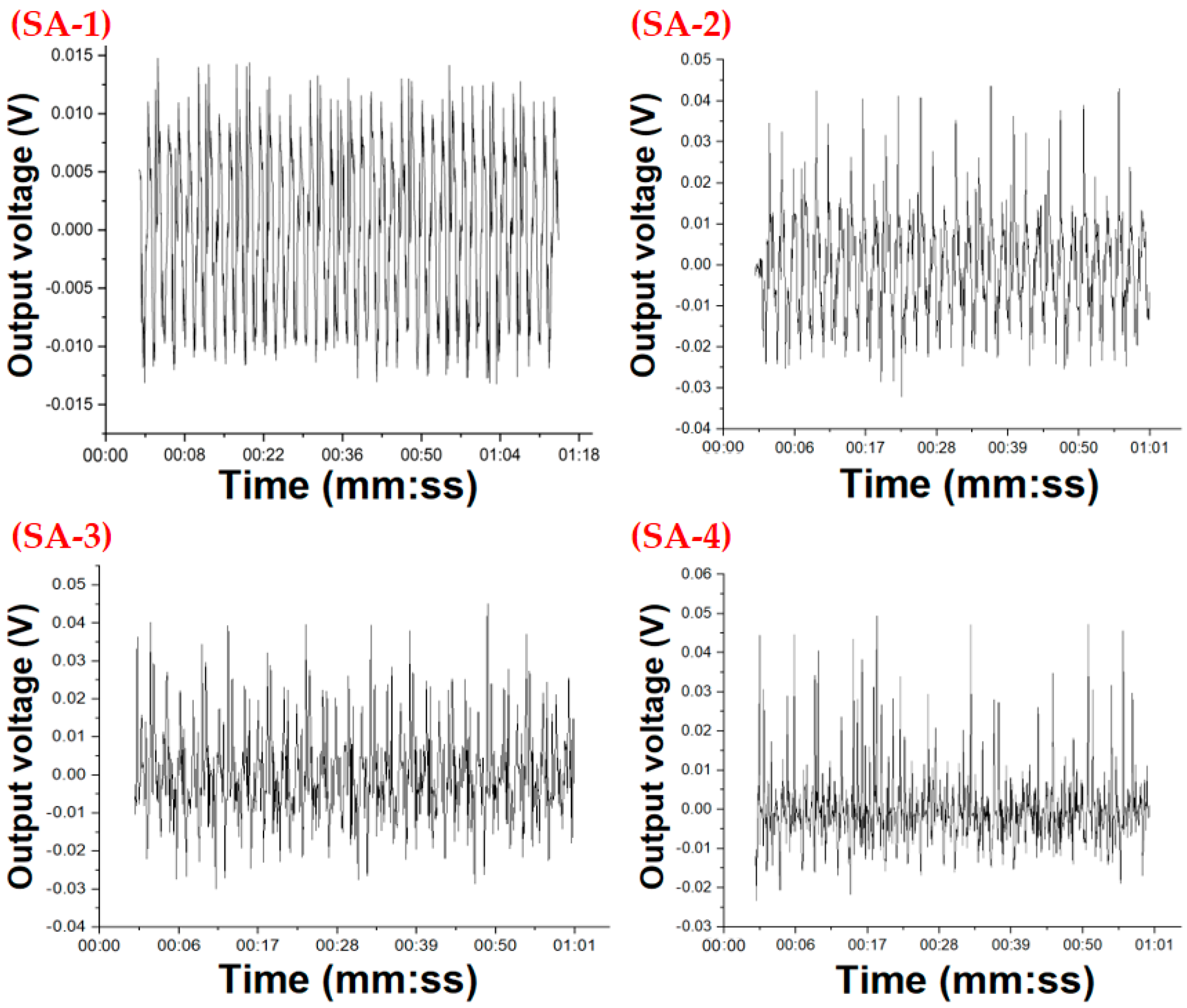
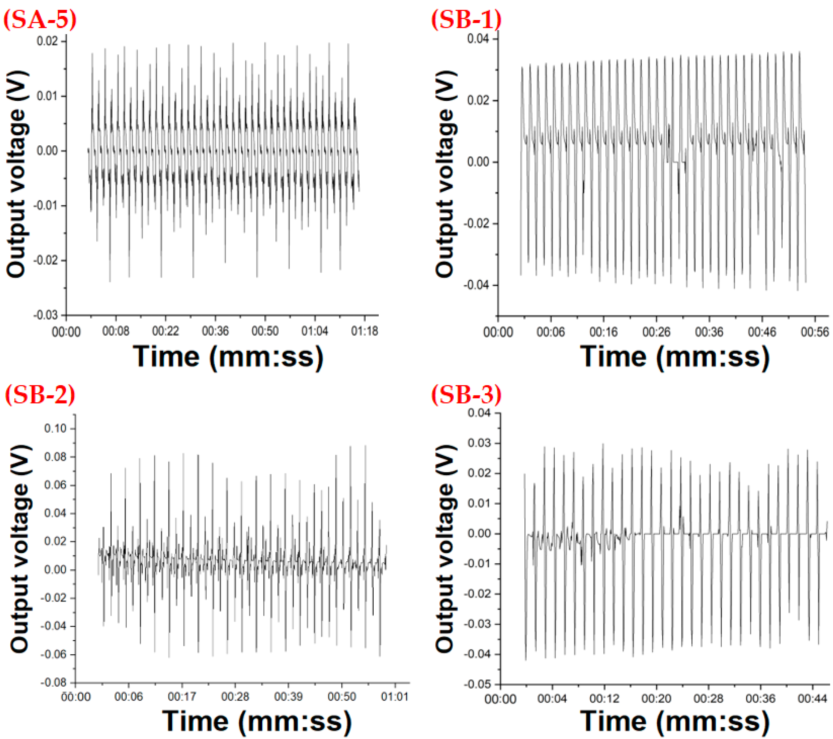
Figure 7.
The raw output voltage graphs that were used to extract the mean peak-to-peak voltages compared in Figure 6 for the eight samples of the Ag/ZnO/Cr/ITO structure that were annealed differently, as denoted in Table 2. The five samples (SA-1 to SA-5) were formed on Al-foil substrates with an ITO layer thickness of 446 nm. The other three samples (SB-1 to SB-3) were formed on the same Al-foil substrate with an ITO layer thickness of 1390 nm.


Figure 8.
LRTEM (200 KeV) cross-sectional image (left) and SAED patterns (right) of the ZnO/Cr/ITO stacked layers deposited on the Al-foil substrate. The SAED patterns indicate that polycrystalline (a) ZnO, (b) Cr, and (c) ITO films were deposited as expected. (d) Polycrystalline face-centered cubic (FCC) structure of the Al film. The scale bar represents 0.5 µm.

Figure 9.
LRTEM (200 KeV) cross-sectional image (left) and EDS depth profile (right) of the ZnO/Cr/ITO/Al-foil stacked films deposited on the Al-foil substrate. The scale bar represents 500 nm.
Figure 9.
LRTEM (200 KeV) cross-sectional image (left) and EDS depth profile (right) of the ZnO/Cr/ITO/Al-foil stacked films deposited on the Al-foil substrate. The scale bar represents 500 nm.

Figure 10.
Design and fabrication of device samples adopting AlN, a-Si (n-type), or SiO2. All the fabricated devices (G–L) were annealed at 300 °C for 1 h in the one-step annealing process defined in Figure 3. The mean peak-to-peak output voltages of the six sample structures (A–F) are compared in the histogram (top). The six sample structure diagrams (G–L) correspond to the mean peak-to-peak output voltage histogram directly above it (A–F) (bottom). Device structures are as follows: (G) Ag/ZnO/Cr/AlN/ITO/Al-foil, (H) Ag/ZnO/AlN/Cr/ITO/Al-foil, (I) Ag/ZnO/Cr/a-Si/ITO/Al-foil, (J) Ag/ZnO/a-Si/Cr/ITO/Al-foil, (K) Ag/ZnO/Cr/SiO2/ITO/Al-foil, and (L) Ag/ZnO/SiO2/Cr/ITO/Al-foil.

Figure 11.
The output voltages of the four different devices (A–D) were investigated to see the effects of ITO on the device performance. The mean peak-to-peak output voltages (top left) and corresponding raw output voltage waveforms (I–L) are shown (right), respectively. Device structures are as follows: (E) Ag/ZnO/AlN/Cr/ITO/Al-foil, (F) Ag/ZnO/AlN/Cr/Al-foil, (G) Ag/ZnO/Cr/AlN/ITO/Al-foil, and (H) Ag/ZnO/Cr/AlN/Al-foil.


Table 1.
Target materials and radio frequency (RF) sputtering conditions used to deposit thin films.
Table 1.
Target materials and radio frequency (RF) sputtering conditions used to deposit thin films.
| Material | RF Power (W) | Film Thickness (nm) | Deposition Time (min) | Gas/Flow Rate (sccm) |
|---|---|---|---|---|
| ITO | 200 | 446 | 30 | Ar/20 |
| 1390 | 90 | |||
| AlN | 80 | 33 | 40 | |
| n-type a-Si | 57 | |||
| SiO2 | 52 | |||
| Cr | 160 | 192 | 30 | |
| ZnO | 200 | 485 | 90 | Ar/18 + N2O/12 |
Table 2.
Sample names and annealing conditions of the eight devices included in Figure 6 and Figure 7.
| Sample Name | SA-1 | SA-2 | SA-3 | SA-4 | SA-5 | SB-1 | SB-2 | SB-3 |
|---|---|---|---|---|---|---|---|---|
| Annealing process | as-deposited | one-step | two-step | one-step | two-step | as-deposited | one-step | two-step |
| Temperature | 300 °C | 300 °C | 400 °C | 400 °C | 300 °C | 400 °C | ||
| Duration | 1 h | 1 h | 1 h | 1 h | 1 h | 0.5 h |
© 2019 by the authors. Licensee MDPI, Basel, Switzerland. This article is an open access article distributed under the terms and conditions of the Creative Commons Attribution (CC BY) license (http://creativecommons.org/licenses/by/4.0/).
Share and Cite
MDPI and ACS Style
Yoon, C.; Jeon, B.; Yoon, G. A Feasibility Study of Fabrication of Piezoelectric Energy Harvesters on Commercially Available Aluminum Foil. Energies 2019, 12, 2797. https://doi.org/10.3390/en12142797
AMA Style
Yoon C, Jeon B, Yoon G. A Feasibility Study of Fabrication of Piezoelectric Energy Harvesters on Commercially Available Aluminum Foil. Energies. 2019; 12(14):2797. https://doi.org/10.3390/en12142797
Chicago/Turabian StyleYoon, Chongsei, Buil Jeon, and Giwan Yoon. 2019. "A Feasibility Study of Fabrication of Piezoelectric Energy Harvesters on Commercially Available Aluminum Foil" Energies 12, no. 14: 2797. https://doi.org/10.3390/en12142797
Note that from the first issue of 2016, this journal uses article numbers instead of page numbers. See further details here.