The Design of a Low Cost Phasor Measurement Unit


Department of Engineering, University of Campania “Luigi Vanvitelli”, 81031 Aversa (CE), Italy
*
Author to whom correspondence should be addressed.
Energies 2019, 12(14), 2648; https://doi.org/10.3390/en12142648
Submission received: 12 June 2019
/
Revised: 1 July 2019
/
Accepted: 6 July 2019
/
Published: 10 July 2019
(This article belongs to the Special Issue Medium/Low Voltage Smart Grids)
Abstract
:The widespread diffusion of Phasor Measurement Units (PMUs) is a becoming a need for the development of the “smartness” of power systems. However, PMU with accuracy compliant to the standard Institute of Electrical and Electronics Engineers (IEEE) C37.118.1-2011 and its amendment IEEE Std C37.118.1a-2014 have typically costs that constitute a brake for their diffusion. Therefore, in this paper, the design of a low-cost implementation of a PMU is presented. The low cost approach is followed in the design of all the building blocks of the PMU. A key feature of the presented approach is that the data acquisition, data processing and data communication are integrated in a single low cost microcontroller. The synchronization is obtained using a simple external Global Positioning System receiver, which does not provide a disciplined clock. The synchronization of sampling frequency, and thus of the measurement, to the Universal Time Coordinated, is obtained by means of a suitable signal processing technique. For this implementation, the Interpolated Discrete Fourier Transform has been used as the synchrophasor estimation algorithm. A thorough metrological characterization of the realized prototype in different test conditions proposed by the standards, using a high performance PMU calibrator, is also shown.
1. Introduction
The need for the best estimate of the power system’s state is recognized to be a crucial element in improving its performance and its resilience to face catastrophic failures. Thus, one of the most important advancement expected from smart grid technology is the strengthening of the management of the power system [1]. Currently, most of the control actions of a power system are performed through an open-loop type centralized control that implements only steady-state security functions. This applies since the Wide Area Measurement Systems (WAMS) typically devoted to this aim have long latency time. This, obviously, places some limits in terms of the level of stability, reliability and safety of the supervised power system. For this reason, in recent years, synchrophasor technologies and the related monitoring devices called Phasor Measurement Units (PMUs) have received a lot of attention [2,3,4,5]. A PMU measures the instantaneous voltage, current, frequency and the Rate Of Change Of Frequency (ROCOF) at specific locations in an electric power transmission system; then, it converts the measured parameters into phasor values, typically with a rate of 25 or more, per second. Finally, it also adds a precise time stamp to these phasor values, turning them into synchrophasors. Time stamping allows these phasor values, provided by PMUs in different locations and across different power industry organizations, to be correlated and time-aligned and so properly combined. The resulting information enables transmission grid planners and operators to have a high-resolution “picture” of the conditions throughout the grid in real time [1]. Thus, with a large-scale implementation of WAMS using PMUs and Phasor Data Concentrators (PDCs) in a hierarchical structure, it become possible to perform a closed loop automatic monitoring and control of the power system to steer it away from transient or voltage instability, through corrective actions initiated during a state of emergency [4,5].
The number of installed PMUs worldwide is constantly increasing; nevertheless, the cost of these devices is still a source of concern for widespread installations, [6,7,8]. Thus, a certain effort in research field is devoted in developing methodology to better observe, understand and manage the grid but limiting the number of installed devices, [9,10,11]. This paper tries to face the same problem but from a different point of view: it proposes a design approach for implementing a PMU only adopting low cost hardware, thus making it possible to use them on a large scale.
In recent years, there have been significant research contributions on the improvement of the PMU performances adopting different algorithms [12,13,14,15,16,17,18,19], or on the PMU-based event detection [20,21]. Few works, to the best of the author’s knowledge, focused on the implementation of this kind of instruments. In [22], an example of PMU for distribution grids is presented; however, the implementation details are not disclosed. More details are given in [23] where the described PMU prototype is based on a field programmable gate array with high performance. Despite this, the chosen hardware platform (i.e., a National Instrument Compact RIO) is quite expensive. In [24], a prototype of a PMU, based on a microcontroller, is presented; the synchronization is obtained through a GPS signal received from a Wireless Fidelity (Wi-Fi) module. No details are given on the synchronization, nor device characterization is presented. In [25], the OpenPMU project, an open platform for the development of PMU technology, is presented. No specific details on hardware implementation but just a rough cost, of about 1000 $, are given; moreover, nothing is said about the instrument performance. In [26], a development of an analog-to-digital converter (ADC) for PMU applications, with GPS synchronization, based on an open hardware development platform, is discussed. It makes use of external devices, such as a GPS receiver, a Phase Locked Loop (PLL) circuit and an ADC, managed by the powerful BeagleBone Black board. Some issues arise: the development board is not an industrial product, so not suitable for harsh environment like substations; moreover, the performance is not accurately evaluated in comparison with a reference instrument. In [27], a technique to lock the sampling frequency of an ADC, managed by a Digital Signal Processor (DSP), is discussed; it does not use a GPS disciplined oscillator, but a simple GPS receiver. It is based on a non-uniform sampling of the signal, since the sampling period is continuously varied between two discrete values. Good synchronization results are shown in the paper; however, the performance is evaluated in a very simple condition, which is a sine wave with constant frequency, amplitude and phase. In fact, the non-uniform sampling may introduce phase noise and worsen the accuracy of synchrophasor phase estimation.
It is worthwhile to emphasize that in all the cited papers, even if the performance is experimentally evaluated, merely rough experiments using signals of a few volt are executed, excluding input transducers. However, it is known that input transducers are typically the major source of uncertainty in measurement chains for power systems [28,29,30,31,32,33,34,35,36,37]; this issue, specifically for PMU application, is also demonstrated in [38].
In this paper, a design approach for a low-cost prototype of PMU, with a detailed description of its hardware and firmware implementation, is presented. In addition, a thorough metrological characterization of the realized prototype is shown: it has been performed using a metrological grade reference instrument, the Fluke 6135A/PMUCAL, using voltage and current levels typical of low voltage power systems, which are similar to those which can be found in primary, or secondary, substations, at the output of Voltage and Current Instrument Transformers (VT and CT). The paper is organized as follows. In Section 2 some basic recalls on PMU are given. Section 3 presents the hardware implementation of the proposed system, including the analog input adaption stage. Section 4 describes the firmware implementation, along with the techniques used to obtain the synchronization and to improve the measurement accuracy. Section 5 shows the metrological characterization of the prototype and, finally, Section 6 draws the conclusions.
2. Fundamentals of PMU
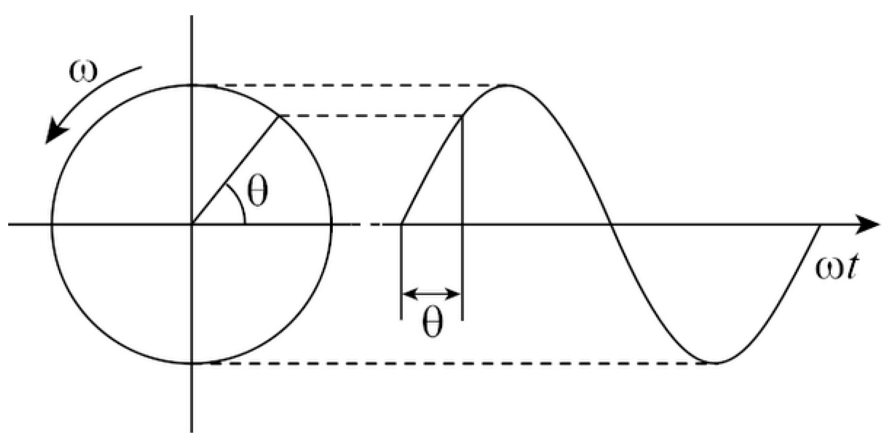
A phasor is a complex number that represents both the magnitude, , and phase angle, , of the voltage or current sinusoidal waveforms pulsating with an angular frequency (with equal to 50 Hz or 60 Hz in different power systems) at a specific point in time (shown in Figure 1).
PMUs measure root mean square (rms) amplitude, phase, frequency and ROCOF of both current and voltage and this collection of grid condition data, which are time-synchronized, is called phasor data. Every PMU measurement obtains a timestamp derived from the GPS universal time. When a phasor measurement is timestamped, it is called a synchrophasor. In this way, PMU measurements performed in different locations can be synchronized and time-aligned and, therefore, combined to provide a detailed view of a wide geographical area. This, moreover, help the system operators to maintain the healthiness of the network.
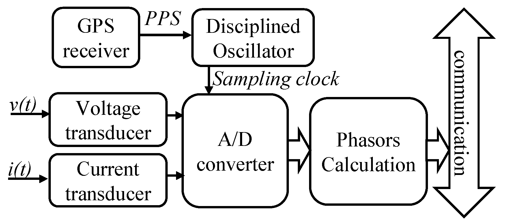
PMUs sample at speeds of up to 50 observations per second (or 60 in USA system), whereas conventional monitoring technologies (such as Supervisory Control And Data Acquisition, SCADA) measure once every two to four seconds. However, in order to allow the comparison of the electrical quantities of the nodes (amplitude and phase of the voltages and currents), the measurements must be made at common sampling instants. The absolute time reference can be used to synchronize the simultaneous sampling of voltage and current signals. The standards [2,3] define the reference time instants in which the PMU must measure the electrical signals and the levels of accuracy that equipment should meet for the various classes of accuracy. In order to face these requirements several test conditions and performance verifications are prescribed. A crucial role in performance verification is played by the synchronization stage: in fact, as it is stated in [2,3], a synchronization error of 1 µs results itself in a Total Vector Error (TVE) of 1 %. All the recalled requirements reflect on the design of a PMU measurement system. A basic architecture, typically adopted for PMU implementation, is reported in Figure 2.
The core of this architecture is the oscillator disciplined by the Pulse Per Second (PPS) signal coming from GPS receiver, which can give a sampling clock accurately synchronized to the absolute time reference, i.e., the Universal Time Coordinated (UTC). In this way, the synchronization requirements are satisfied as the analog signals are sampled synchronously with the absolute time reference. Nevertheless, the GPS Disciplined Oscillator (GPSDO) is not a cheap component and, to obtain a low-cost implementation, this component should be removed.
In addition, as is demonstrated in [38], the input transducers and the analog signal conditioning stages could be the major source of uncertainty in PMU measurement systems. Therefore, particular attention should be also paid to the design and usage of these components.
3. Hardware Implementation
3.1. System Architecture
In order to obtain an adequate level of accuracy and, at the same time, keep low the hardware cost, reference is made to the architecture reported in Figure 3 and only cheap components have been chosen. The input stages are constituted by low cost voltage and current transducers equipped with suitable analog conditioning stages to adapt the signal level to the input range of the ADC. The core of the instrument is a low-cost Advanced Reduced Instruction Set Computer (RISC) Machine (ARM) microcontroller unit (MCU) with integrated ADC (analog-to-digital converter) and Ethernet interface. It is responsible for the absolute time synchronization, data acquisition, signal processing and data communication. A key feature of the design is the lack of a GPSDO. Instead, a simple GPS receiver is used and all the synchronization is derived by the PPS signal. Therefore, a suitable signal processing is adopted to obtain measurements synchronized to the UTC, as it is better explained in Section 4. Voltage and current synchrophasors, frequency and ROCOF are obtained by processing the synchronized signal samples through an Interpolated Discrete Fourier Transform (IpDFT) algorithm [14]. Measurement data are communicated through a Transmission Control Protocol (TCP) socket to a host Personal Computer (PC); for the scope of this work, the standard Institute of Electrical and Electronics Engineers (IEEE) Std C37.118.2-2011 [39] has not been considered.
3.2. Input Stage
The used voltage and current transducers are the LEM LV 25-P and the LEM LA 25-NP, respectively. Their conditioning circuits have been designed as simple as possible, using the lowest number of active components as possible, in order to keep, at the same time, the cost low and the signal-to-noise ratio as high as possible. The conditioning circuit for the voltage transducer is shown in Figure 4, where T1 represents the transducer. It converts a rated rms input current of 10 mA in a current of 25 mA, with a maximum rms input voltage of 700 V. The input signal range has been considered limited to a rms value of 300 V so the input resistance is chosen equal to obtaining an output bipolar current of 25 mA. Then, in order to obtain a peak-to-peak unipolar voltage output of about 3.3 V (i.e., the input range of the microcontroller ADC) a resistor is inserted in series and an offset voltage of 1.65 V, directly derived from ADC reference voltage, is added as shown in Figure 4. The values of the other components are (in order to drain a maximum current of about 170 from the microcontroller) and (in order to cut high frequency noise). The adopted current conditioning circuit is very similar to that previously presented for voltage, the only difference in the scheme is that current transducer has no need of input resistance.
3.3. Microcontroller
The signals obtained from input stages are directly connected to two analog inputs of a STM32F407V MCU. This microcontroller is based on an ARM Cortex-M4 32 bit core with Floating Point Unit (FPU), it reaches 210 Dhrystone Mega Instructions Per Second (DMIPS) running at 168 MHz clock. It carries 512 kB of Flash and 192 kB of Static Random Access Memory (SRAM). It integrates several peripheral: Universal Serial Bus On-The-Go (USB OTG) HS/FS, Ethernet, 17 timers, three ADCs, 15 communication interfaces and camera interface. For this project, different features of MCU are used: two different 12-bit ADCs to acquire input signals, two internal 16-bit timers running at 168 MHz for timing and synchronization management, a Universal Asynchronous Receiver Transmitter (UART) to communicate with GPS receiver, an external input interrupt to receive the PPS signal and the Ethernet Media Access Control (MAC) interface to implement communication.
3.4. GPS Receiver
It is worthwhile to underline that, for cost reasons, only simple GPS receivers without disciplined oscillator output have been considered and an external Original Equipment Manufacturer (OEM) GPS receiver module Linx-rxm-GPS-FM has been chosen. It is a self-contained receiver based on the MediaTek MT3339 chipset, it can simultaneously acquire on 66 channels and track on up to 22 channels. This gives the module fast lock times even at low signal levels. The module outputs standard National Marine Electronics Association (NMEA) data messages through a UART interface.
4. Firmware Implementation
The firmware is fully developed in C language; Keil Microcontroller Development Kit (MDK) ARM development environment has been chosen for its high performance toolchain. The presented work has been developed on a low cost microcontroller, with relatively poor hardware features; consequently, great challenges are constituted by the firmware optimization and the accurate metrological characterization to evaluate and compensate the systematic errors. In particular, the main challenges have been related to: (1) the lack of specific synchronization hardware, (2) the lack of high resolution 32-bit timer at 168 MHz, (3) the poor Digital Signal Processing (DSP) performance of the floating-point unit (it does not implement 64 bit double-precision calculations) and (4) the low RAM size. In this section, some details on the main parts of firmware will be described, along with the techniques adopted to overcome the hardware limitations.
4.1. Synchronization
A PMU shall be capable to receive time synchronization from a reliable and accurate source, such as the GPS, and to perform phasor measurements synchronized to UTC time, with accuracy sufficient to meet the requirements specified in the standards [2,3]. It should perform all the measurements and report the results at a constant reporting rate, expressed in terms of frames per second (fps). The reporting rate is an integer number (i.e., 50/60 fps, 25/30 fps, 10/12 fps, etc.) and it defines the reporting time instants at which the PMU shall report the measurement results. For a reporting rate N fps, the N reporting times are evenly spaced through each second with first reporting time coincident with the UTC second rollover (e.g., coincident with a 1 PPS provided by GPS, see Figure 5). The typical solution adopted by commercial PMUs is the use of a 10 MHz GPSDO. Starting from this system clock, a sampling clock is derived, so that also sampling instants are referenced to UTC and the constraint of evenly spaced measurements is simply obtained by performing analysis on a constant number of samples (see Figure 6). In this paper, with the aim of cost saving, a different approach, based on a cheap GPS receiver and on a complex firmware technique based on numeric synchronization and resampling, is proposed. In the presented prototype, the internal MCU clock is not disciplined and, thus, it is not aligned to absolute time (see Figure 7). Moreover, it is obtained by multiplying the output frequency of a low cost quartz crystal through the PLL circuit (integrated in the MCU) and so affected by frequency jitter and thermal drift; its frequency (168 MHz), however, is much higher than the typical GPSDO frequency. Therefore, the system clock and internal timers are used to build a reference time-base (TB) and a firmware procedure manages the timers to keep their rollover periodicity locked to PPS and thus to UTC absolute time. To this aim, an internal counter (Time-Base Counter, TBC), running at 168 MHz, is used and configured with a counting number that is continuously estimated and corrected to keep its periodicity as close as possible to an integer fraction of 1 s (i.e., 1 s/50 = 20 ms). In fact, at each PPS event coming from the GPS receiver, a specific Interrupt Service Routine (ISR) calculates how many system ticks have been elapsed from the previous PPS event. This number is used to correct the counting number adopted in the next second to produce a counter rollover each 20 ms: the number of ticks, divided by 50, is the fractional number of ticks that corresponds to 20 ms and it defines the reporting time at 50 fps, the maximum reporting rate considered (i.e., related to 50 Hz power frequency). Obviously, since the number of ticks, divided by 50, can be a decimal number, whereas the counter accepts only integer numbers, a specific management strategy, explained in Section 4.3, has been used. Other reporting rates can be obtained by decimation. The correction is calculated adopting a discrete Proportional Integrative Derivative (PID) control algorithm, as better explained in Section 4.2. In this way, since the counter rollover is precisely produced every 20 ms (i.e., 50 pulses per second, 50-pps), it can be used to obtain the synchronized reporting time instants. However, in order to have synchronized measurements of the phasor, having a synchronized TB is not enough. In fact, it is necessary to sample the input signals synchronously with the absolute time reference, which is not the case at hand. Therefore, at each TB rollover, MCU takes and stores, in a dedicated queue, the timing information needed to perform a signal resampling, that is the number of ticks elapsed from last sampling time, called control info (CI). In fact, with CI, the actual synchronized sampling instants are estimated and then the acquired data are resampled with linear interpolation, in order to have a signal synchronously sampled. The data acquired between two subsequent TB events is called frame. The subsequent processing stage manipulates the frames and extracts the phasors.
4.2. PID Control
As previously mentioned, to keep the internal TB phase locked with the PPS, a specific ISR takes the number of system ticks elapsed from the last PPS event and feeds a PID control algorithm. More in details, at each PPS event, the ISR snapshots the count value of the TBC, it computes the deviation, , with respect to the values obtained at previous PPS event, and it feeds the PID. The output of the PID, divided by 50, will be the value used to configure the TBC rollover for the next second, as better explained in Section 4.3. In details, the new reload values , at j-th iteration, can be computed as:
where is the reference number of ticks, is the current value of counted ticks and , and are, respectively, proportional, integrative and derivative components. Note that is computed recursively and is approximated as backward finite difference. Since the transfer function of the system is not known, the PID constants (, and ) have been determined with the Ziegler-Nichols approach and empirically adjusted. The PID can act only one time per second, because reference time is only available one time per second (each PPS event). Moreover, a little value for constant has been chosen in order to obtain a low jitter in steady state conditions. This leads to a quite slow locking to absolute time, many iterations (between 60 and 80, depending on initial phase displacement) are needed to stably converge around the reference; thus, the anti-windup technique and the preload of integrator constant have been implemented to make the system work correctly within a few second after startup. In conclusion, the PID action keeps the TB of 50-pps locked in phase to the 1-PPS signal received by the GPS.
The accuracy of synchronization was experimentally evaluated: the time intervals between the active edges of the PPS signal and obtained time base periodicity have been measured with a 12-bit Lecroy MDA810 digital storage oscilloscope for about some hours. The measured distribution of the time delay is shown in Figure 8. Deviation, at steady state, exhibits almost a normal distribution with a mean systematic delay of 1.25 µs and maximum error of 500 ns. Thus, the system satisfactory reacts to internal clock drift and jitter obtaining good synchronization accuracy.
4.3. Time-Base
The TB is a crucial part of the system as it has been used to trigger all the calculations. As previously described, the TB relies on an internal high-resolution timer, with a clock frequency as higher as possible to reach the best accuracy possible. High counter frequency implies that the counted number rapidly increases so that a 32-bit timer would be appropriate to implement the TBC. Unfortunately, a 32-bit timer running at system core clock is not a common feature on low cost MCUs; additionally, the adopted MCU has no 32-bit timers at 168 MHz but it has only 16-bit timers and it is not possible to perform a direct hardware cascade connection of two 16-bit timers (to obtain one single 32-bit timer from two 16-bit timers). To face these hardware limitations, a firmware technique to cascade two 16-bit counters for the TBC implementation has been implemented. When the first counter rollover occurs, an ISR manages the working of a second counter until the desired value is reached; particular attention has been paid to insure that the second counter stops before rollover. In the following, for sake of clarity, a numerical example is given for the explanation of the technique. Suppose that the system clock frequency is exactly equal to the nominal value, 168 MHz; in this case, to obtain the 20 ms periodicity for TB, it is needed to count up to 168,000,000/50 = 3,360,000 (reload value for TB), which is a number not representable with 16-bit. For this reason, the firmware lets the 16-bit counter to reach the rollup (so counting up to 216) for a number of times equal to floor (3,360,000/216) = 51 and, on the 52-th iteration, the counter must be stopped before rollover; on the last iteration it must count 17,664, so reaching the desired value (51 × 216 + 17664 = 3,360,000). Another issue in the implementation of TB comes from the fact that the output of the PID, , is the current tick number that corresponds to 1 s. This value has to be divided by 50 to obtain the TBC reload value to obtain a periodicity of 20 ms (50 fps). It is apparent that the result of the division is, in general, a decimal number while the TBC reload must be an integer number. A straightforward rounding of this value leads to a loss in resolution that could be relevant for the aimed application. Therefore, to mitigate this effect, the decimal part is properly considered: when, at the PPS event, a new TBC reload is calculated, in the next 50 TB events not always the same value is loaded. In fact, firmware reloads 50 potentially different TB values and the i-th reload value is calculated as:
where square parenthesis means rounding to nearest integer. With this formula, the summation of the 50 TB values will always coincide with .
4.4. AD Conversion
Two different ADC are used to acquire voltage and current signals and, to obtain simultaneous sampling, an internal timer has been selected as trigger source for both ADCs. The chosen sampling frequency was 6400 Hz as it corresponds to 128 samples per cycle at 50 Hz and the basic sampling time instants are triggered by a high-resolution timer running at system clock of 168 MHz. The desired sampling periodicity is obtained loading in the timer a proper counting value that nominally can be calculated dividing the rated system clock by the desired sampling frequency. However, the actual counting value has been experimentally evaluated. A square wave, with frequency equal to the desired sampling frequency has been generated. Its frequency has been measured with the frequency counter Agilent 53230A for some hours. The counting value has been chosen in such a way that the measured frequency of the square wave was as close as possible to 6.4 kHz; in particular, a sampling frequency of 6400.2500 Hz has been chosen, with a standard deviation of 100 µHz, which corresponds to about 0.02 µHz/Hz. The ADCs nominal resolution is 12-bit; nevertheless, for the purpose of the developed project, the effect of noise on the analog input or amplitude quantization can remarkably affect the overall accuracy of the results. Thus, ADC characteristics was enhanced through a technique based on over-sampling and averaging [40], thus obtaining improvement both in terms of amplitude resolution and noise rejection. Therefore, when a sampling time instant is triggered, the ADC is configured to acquire 16 samples at a burst sampling frequency much greater than the chosen sampling frequency (588 kHz). It is worthwhile noting that 16 samples are acquired in a really short time of about 27 µs, much lower than the equivalent sampling time interval. Then, the acquired samples are averaged to obtain the final sampling results. To this aim, two direct memory access channels are configured to simultaneously serve the two ADCs. They copy the samples in dedicated queues and an ISR averages the 16 samples of voltage and current, respectively, using the integrated DSP unit. The averaged results are pushed in two different queues, one for voltage and one for current. A final issue is related to the time collocation of the averaged values: they are the result of the averaging of 16 samples over 27 µs. They are considered at the center of the averaging interval and so a systematic phase delay is introduced; however, this phase delay can be compensated with a correction of the measured synchrophasor phase value returned by the estimation algorithm.
4.5. Resampling
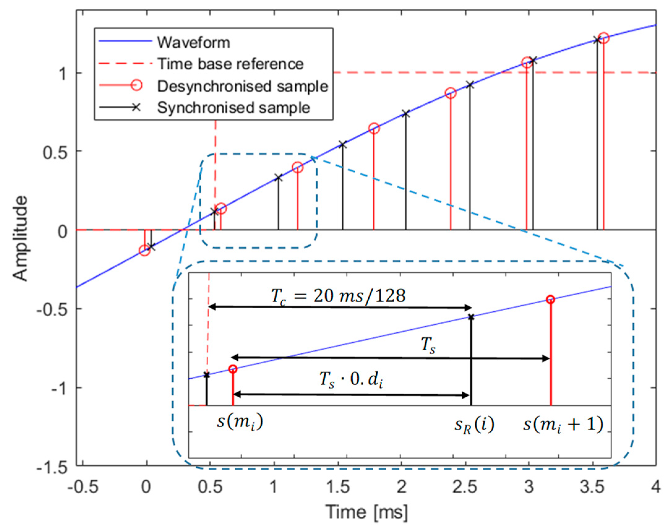
As previously described, to correctly measure a synchrophasor, the input signals must be synchronously sampled with the UTC. In the considered prototype, the sampling time instants are asynchronous with UTC, so they cannot be used directly for synchrophasor calculation for different reasons: (1) the number of samples is different from nominal value (128 samples) in each 20 ms frame, (2) the actual number of samples that corresponds to 20 ms is not an integer number of samples and (3) the first sample of each frame is not aligned with an event of TB. Therefore, the desynchronized acquired signal is resampled with linear interpolation: we can calculate an approximation of the synchronized sample by interpolating the two acquired samples that are closer to the desired time position. Obviously, a more complex interpolation technique can improve the overall accuracy of the instrument. The first step for the resampling is to put in relation the desynchronized and synchronized time instants. The synchronized time instants can be easily obtained starting from TB events, with a uniform spacing of = 20 ms/128 (see Figure 9). The desynchronized time instants, , are spaced of sampling period estimated in the k-th frame. The data needed for estimating are collected by the TB ISR in CI and they are placed in a dedicated queue. In particular, CI includes:
- N, the number of samples acquired in the k-th frame;
- , the value of the system clock counts (systick) read when the last event of the TB occurs;
- PPStick, the systick read when the last PPS event occurs.
So can be estimated as:
where is the sampling frequency estimated in the k-th frame. With this information, it is possible to find out what are the nearest acquired samples, by calculating where the synchronized samples should be “virtually” located in the acquisition buffer. These “virtual locations” of the i-th synchronized sample, , come out by dividing the synchronized time instants,, by the measured sampling period, :
where are not-integer indexes, with an integer part, , and a decimal part, . Thus, the i-th synchronized sample should have been acquired between the actual acquired samples, that are at indexes mi and mi + 1 of the buffer, with a normalized distance from the former of 0.di and with a distance from the latter of 1 − 0.di (see Figure 4). Therefore, an estimation of the i-th synchronized sample, , can be calculated as average of two nearest samples weighted according relative distances thus:
where and are two subsequent acquired samples, closest to the i-th synchronized time instants (see Figure 9). With this approach, 512 synchronized samples are calculated so that, the first half is taken before, and the other half is taken after each synchronized TB event.
4.6. Synchrophasor Calculation
To estimate the synchrophasor, different techniques were proposed [13,14,15,16,17,18,19] in scientific literature. Most of them are eligible to be implemented in the proposed prototype; for this paper, the technique based on interpolation in the frequency domain is chosen [14]. The algorithm starts with calculating Discrete Fourier Transform (DFT) of resampled values. These samples are synchronous with absolute time but, in general, asynchronous with respect to the power system frequency. Thus, none of the calculated spectral components exactly matches with the fundamental components of the acquired signals. Nevertheless, its actual amplitude, phase angle and frequency can be evaluated by interpolating the obtained spectral components. This procedure can be adopted on the assumption of negligibility of the spectral leakage effects due to other sinusoidal components and due to spectral replica at negative frequency. This assumption can be made adopting an opportune window like Hanning window that has good performance, relatively to attenuation of spectral leakage [14]. For the case at hand, the effect of negative replica results to be prevalent and iterative estimation procedure was adopted to make this effect negligible.
4.7. Execution Times
All the execution times of the different routines of the implemented firmware have been measured. In particular, the maximum reporting rate has been considered, that is 50 Hz, and an observation interval of four cycles of nominal power frequency (50 Hz) has been used. Each execution time has been measured in this way: a digital pin of the microcontroller has been set to high value just before the execution of the specific routine and again set to low value just after the routine execution; the duration of the obtained pulse was measured with the 12-bit Lecroy MDA810 digital storage oscilloscope. The results are as follows: (1) PID routine takes 1.6 µs every 1 s, (2) TB routine takes 2.5 µs every 20 ms (50 times a second), (3) oversampling and averaging take 3 µs every 156 µs (6400 times a second), (4) extraction from queue routine takes 2.2 µs every 20 ms (50 times a second), (5) time domain interpolation takes 6.8 ms every 20 ms (50 times a second), (6) IpDFT takes 560 µs every 20 ms (50 times a second). Summarizing, the total execution time is 7.8 ms for the two channels, i.e., quite lower than 20 ms, which is the time interval between two reporting instants.
5. Experimental Results
The realized PMU prototype has been tested with a high performance PMU calibrator, the Fluke 6135A/PMUCAL.
A metrological characterization of the calibrator has been performed, by some of the authors, in [38]. It is able to give reliable results down to values of 0.012% for TVE, 0.6 mHz for Frequency Error (FE) and 0.07 Hz/s for Rate of change of Frequency Error (RFE), in the various test conditions of [2,3].
The presented prototype has been tested in several testing conditions, both for class P as well as for class M PMUs, as prescribed in [2,3], for rated voltage of 230 V and rated current of 10 A. The chosen testing conditions are:
- Sinewaves with off-nominal frequency deviations within ±2 Hz (class P) and ±5 Hz (class M);
- Sinewaves with off-nominal frequency deviations within ±2 Hz (class P) and ±5 Hz (class M) affected by one single harmonic component, from 2nd to 50th, of amplitude equal to 1% (class P) and 10% (class M) of the fundamental;
- Amplitude Modulated (AM) sinewaves affected by a 2 Hz (class P) and 5 Hz (class M) modulating tone of amplitude equal to 10% of the fundamental;
- Phase Modulated (PM) sinewaves affected by a 2 Hz (class P) and 5 Hz (class M) modulating tone of amplitude equal to 0.1 rad;
- 50 Hz sinewaves corrupted by a single out-of-band inter-harmonic (only class M) of amplitude equal to 10% of the fundamental at 24.9 Hz;
- Chirp waveforms with the fundamental frequency increasing linearly from about 48 Hz to 52 Hz (class P) and from 45 Hz to 55 Hz (class M), and vice versa, at a rate of ±1 Hz/s.
Results of the experimental tests are summarized in Table 1 (class P) and Table 2 (class M). They were obtained using an observation interval of four nominal 50 Hz cycles and a reporting rate of 50 fps. For sake of brevity, only results relative to voltage channel are presented; similar values have been obtained also for current channel.
The IpDFT algorithm generally shows good performance in steady-state conditions, in particular in presence of harmonics and inter-harmonics. Nevertheless, the performance is worse in dynamic conditions (with frequency ramp and especially with amplitude and phase modulations). These results are essentially due to the static phasor model at the base of the IpDFT and become worse with the increase of the time observation window.
However, it can be seen that the TVE, FE and RFE are below the standard limits for practically all the testing conditions, except for the out-of-band interharmonic, where both TVE and FE are over the limit, and for the frequency ramp for class M, where the RFE is slightly worse (0.21 Hz/s) than the limit (0.20 Hz/s).
These results are particularly relevant especially if compared with the results shown in [38], where the experimental characterization of the IpDFT algorithm is performed using a high-performance measuring hardware, constituted by a PXI controller, 16-bit data acquisition system, high accuracy class voltage and current transducers and a synchronization board acting as GPSDO.
The performance here shown is, as expected, worse, due to the intrinsic poor performance of the hardware here used; however, some situations, where errors are near (or over) the limit, are highlighted also in [38], thus depending essentially on the used estimation algorithm.
6. Conclusions
In this paper, a design approach for the realization of a very low cost PMU is presented. The core of the instrument is an ARM microcontroller with integrated ADC and Ethernet controller. External devices are used to realize the voltage and current sensing stage, a simple GPS receiver is used to receive the PPS and the timestamp and, in particular, no GPS disciplined oscillator has been used.
Since a key feature of the PMU is the accurate synchronization with UTC, in order to meet this requirement with a sufficient accuracy, and without specific synchronization hardware, an efficient signal processing synchronization technique has been used, which is able to lock the sampling frequency to the UTC. To verify the robustness of the proposed design approach, a very common phasor estimation algorithm, the IpDFT, has been implemented onboard the microcontroller. Its features are the ease to implement and the quite low computational complexity.
The cost of the prototype is very low, about 110 €, obtained in this way: (1) the transducer cost is about 90 €, (2) the cost of the microcontroller development board is about 10 €, (3) the cost of the GPS receiver and the antenna is lower than 10 € and (4) the electronic components of the conditioning circuit is lower than 1 €.
The realized prototype has been tested with a high performance PMU calibrator, the Fluke 6135A/PMUCAL, in several testing conditions reported in [2,3]. The maximum values for TVE, FE and RFE are below the standard limits practically for every testing condition, except for interharmonic, and for RFE in the frequency ramp test for Class M PMUs. However, comparing the obtained results with those obtained from an IpDFT implementation on a high performance measuring hardware [38], nearly the same issues have been found.
Author Contributions
Conceptualization, M.L.; methodology, C.L. and D.G.; software, A.D.F.; validation, M.L. and A.D.F.; formal analysis, C.L. and D.G.; investigation, M.L., C.L., D.G. and A.D.F.; resources, M.L. and C.L.; data curation, A.D.F.; writing—original draft preparation, M.L. and A.D.F.; writing—review and editing, C.L. and D.G.; supervision, C.L.; funding acquisition, M.L. and C.L.
Funding
The work presented in this paper was funded by European Metrology Programme for Innovation and Research (EMPIR), 17IND06 Future Grid II project, which is jointly funded by the EMPIR participating countries within EURopean Association of national METrology institutes (EURAMET) and the European Union.
Conflicts of Interest
The authors declare no conflict of interest.
References
- Bose, A. Smart transmission grid applications and their supporting infrastructure. IEEE Trans. Smart Grid 2010, 1, 11–19. [Google Scholar] [CrossRef]
- IEEE Standard for Synchrophasor Measurements for Power Systems. In IEEE Std C37.118.1-2011 (Revision of IEEE Std C37.118-2005); IEEE: Piscataway, NJ, USA, 2011; pp. 1–61. [CrossRef]
- IEEE Standard for Synchrophasor Measurements for Power Systems—Amendment 1: Modification of Selected Performance Requirements. In IEEE Std C37.118.1a-2014 (Amendment to IEEE Std C37.118.1-2011); IEEE: Piscataway, NJ, USA, 2014; pp. 1–25. [CrossRef]
- De La Ree, J.; Centeno, V.; Thorp, J.S.; Phadke, A.G. Synchronized Phasor Measurement Applications in Power Systems. IEEE Trans. Smart Grid 2010, 1, 20–27. [Google Scholar] [CrossRef]
- Silverstein, A. Synchrophasors & the Grid. In Proceedings of the Electricity Advisory Committee Meeting, Arlington, VA, USA, 13 September 2017. [Google Scholar]
- U.S. Department of Energy. Advancement of Synchrophasor Technology in Projects Funded by the American Recovery and Reinvestment Act of 2009; U.S. Department of Energy: Washington, DC, USA, 2016.
- U.S. Department of Energy. Office of Electricity Delivery and Energy Reliability, Factors Affecting PMU Installation Costs; U.S. Department of Energy: Washington, DC, USA, 2014.
- Lelic, D. PMU Cost & Benefits Study. In Proceedings of the Center for Advanced Power Engineering Research Meeting. Available online: http://caper-usa.com/wp-content/uploads/2017/08/Session-IV-PMU-Cost-Benefits-Studies-DLelic_8-8-17.pdf (accessed on 10 July 2019).
- Baldwin, T.L.; Mili, L.; Boisen, M.B.; Adapa, R. Power system observability with minimal phasor measurement placement. IEEE Trans. Power Syst. 1993, 8, 707–715. [Google Scholar] [CrossRef]
- Nuqui, R.F.; Phadke, A.G. Phasor measurement unit placement techniques for complete and incomplete observability. IEEE Trans. Power Deliv. 2005, 20, 2381–2388. [Google Scholar] [CrossRef]
- Zhong, Z.; Xu, C.; Billian, B.J.; Zhang, L.; Tsai, S.-J.S.; Conners, R.W.; Centeno, V.A.; Phadke, A.G.; Liu, Y. Power system frequency monitoring network (FNET) implementation. IEEE Trans. Power Syst. 2005, 20, 1914–1921. [Google Scholar] [CrossRef]
- Phadke, A.G.; Kasztenny, B. Synchronized Phasor and Frequency Measurement Under Transient Conditions. IEEE Trans. Power Deliv. 2009, 24, 89–95. [Google Scholar] [CrossRef]
- De la O Serna, J.A.; Platas, M.A. Maximally flat differentiators through WLS Taylor decomposition. Elsevier Digit. Signal Process. 2011, 21, 183–194. [Google Scholar] [CrossRef]
- Belega, D.; Petri, D. Accuracy Analysis of the Multicycle Synchrophasor Estimator Provided by the Interpolated DFT Algorithm. IEEE Trans. Instrum. Meas. 2013, 62, 942–953. [Google Scholar] [CrossRef]
- Petri, D.; Fontanelli, D.; Macii, D. A Frequency-Domain Algorithm for Dynamic Synchrophasor and Frequency Estimation. IEEE Trans. Instrum. Meas. 2014, 63, 2330–2340. [Google Scholar] [CrossRef]
- Bertocco, M.; Frigo, G.; Narduzzi, C.; Muscas, C.; Pegoraro, P.A. Compressive Sensing of a Taylor-Fourier Multifrequency Model for Synchrophasor Estimation. IEEE Trans. Instrum. Meas. 2015, 64, 3274–3283. [Google Scholar] [CrossRef]
- Cuccaro, P.; Gallo, D.; Landi, C.; Luiso, M.; Romano, G. Recursive phasor estimation algorithm for synchrophasor measurement. In Proceedings of the 2015 IEEE International Workshop on Applied Measurements for Power Systems (AMPS), Aachen, Germany, 23–25 September 2015; pp. 90–95. [Google Scholar]
- Cuccaro, P.; Gallo, D.; Landi, C.; Luiso, M.; Romano, G. Phase-based estimation of synchrophasors. In Proceedings of the 2016 IEEE International Workshop on Applied Measurements for Power Systems (AMPS), Aachen, Germany, 28–30 September 2016; pp. 1–6. [Google Scholar]
- Tosato, P.; Macii, D.; Luiso, M.; Brunelli, D.; Gallo, D.; Landi, C. A Tuned Lightweight Estimation Algorithm for Low-Cost Phasor Measurement Units. IEEE Trans. Instrum. Meas. 2018, 67, 1047–1057. [Google Scholar] [CrossRef]
- Jiang, J.A.; Yang, J.Z.; Lin, Y.H.; Liu, C.W.; Ma, J.C. An adaptive PMU based fault detection/location technique for transmission lines. I. Theory and algorithms. IEEE Trans. Power Deliv. 2000, 15, 486–493. [Google Scholar] [CrossRef]
- Tate, J.; Overbye, T.J. Line Outage Detection Using Phasor Angle Measurements. IEEE Trans. Power Syst. 2008, 23, 1644–1652. [Google Scholar] [CrossRef]
- Von Meier, A.; Culler, D.; McEachern, A.; Arghandeh, R. Microsynchrophasors for distribution system. In Proceedings of the 5th IEEE PES Innovative Smart Grid Technologies Conference (ISGT), Washington, DC, USA, 19–22 February 2014; pp. 1–5. [Google Scholar]
- Romano, P.; Paolone, M. Enhanced interpolated-DFT for synchrophasor estimation in FPGAs: Theory, implementation, and validation of a PMU prototype. IEEE Trans. Instrum. Meas. 2014, 63, 2824–2836. [Google Scholar] [CrossRef]
- Das, H.P.; Pradhan, A.K. Development of a micro-phasor measurement unit for distribution system applications. In Proceedings of the National Power Systems Conference (NPSC), Bhubaneswar, India, 19–21 December 2016; pp. 1–5. [Google Scholar]
- Laverty, D.M.; Best, R.J.; Brogan, P.; al Khatib, I.; Vanfretti, L.; Morrow, D.J. The OpenPMU Platform for Open-Source Phasor Measurements. IEEE Trans. Instrum. Meas. 2013, 62, 701–709. [Google Scholar] [CrossRef]
- Zhao, X.; Laverty, D.M.; McKernan, A.; Morrow, D.J.; McLaughlin, K.; Sezer, S. GPS-Disciplined Analog-to-Digital Converter for Phasor Measurement Applications. IEEE Trans. Instrum. Meas. 2017, 66, 2349–2357. [Google Scholar] [CrossRef] [Green Version]
- Yao, Y.; Zhan, L.; Liu, Y.; Till, M.J.; Zhao, J.; Wu, L.; Teng, Z. A Novel Method for Phasor Measurement Unit Sampling Time Error Compensation. IEEE Trans. Smart Grid 2018, 9, 1063–1072. [Google Scholar]
- Cataliotti, A.; di Cara, D.; Emanuel, A.E.; Nuccio, S. Improvement of Hall Effect Current Transducer Metrological Performances in the Presence of Harmonic Distortion. IEEE Trans. Instrum. Meas. 2010, 59, 1091–1097. [Google Scholar] [CrossRef]
- Faifer, M.; Laurano, C.; Ottoboni, R.; Toscani, S.; Zanoni, M. Characterization of Voltage Instrument Transformers Under Nonsinusoidal Conditions Based on the Best Linear Approximation. IEEE Trans. Instrum. Meas. 2018, 67, 2392–2400. [Google Scholar] [CrossRef]
- Crotti, G.; Delle Femine, A.; Gallo, D.; Giordano, D.; Landi, C.; Letizia, P.S.; Luiso, M. Calibration of Current Transformers in distorted conditions. In Journal of Physics: Conference Series; IOP Publishing: Bristol, UK, 2018. [Google Scholar] [CrossRef]
- Del Prete, S.; Delle Femine, A.; Gallo, D.; Landi, C.; Luiso, M. Implementation of a distributed Stand Alone Merging Unit. In Journal of Physics: Conference Series; IOP Publishing: Bristol, UK, 2018. [Google Scholar] [CrossRef]
- Crotti, G.; Delle Femine, A.; Gallo, D.; Giordano, D.; Landi, C.; Luiso, M. Measurement of the Absolute Phase Error of Digitizers. IEEE Trans. Instrum. Meas. 2019, 68, 1724–1731. [Google Scholar] [CrossRef]
- Crotti, G.; Giordano, D.; Delle Femine, A.; Gallo, D.; Landi, C.; Luiso, M. A Testbed for Static and Dynamic Characterization of DC Voltage and Current Transducers. In Proceedings of the 9th IEEE International Workshop on Applied Measurements for Power Systems (AMPS), Bologna, Italy, 26–28 September 2018; pp. 1–6. [Google Scholar] [CrossRef]
- Collin, A.J.; Delle Femine, A.; Gallo, D.; Langella, R.; Luiso, M. Compensation of Current Transformers’ Non-Linearities by Means of Frequency Coupling Matrices. In Proceedings of the 9th IEEE International Workshop on Applied Measurements for Power Systems (AMPS), Bologna, Italy, 26–28 September 2018; pp. 1–6. [Google Scholar] [CrossRef]
- Delle Femine, A.; Gallo, D.; Giordano, D.; Landi, C.; Luiso, M.; Signorino, D. Synchronized Measurement System for Railway Application. In Journal of Physics: Conference Series; IOP Publishing: Bristol, UK, 2018. [Google Scholar] [CrossRef]
- Cataliotti, A.; Cosentino, V.; Crotti, G.; Femine, A.D.; Di Cara, D.; Gallo, D.; Giordano, D.; Landi, C.; Luiso, M.; Modarres, M.; et al. Compensation of Nonlinearity of Voltage and Current Instrument Transformers. IEEE Trans. Instrum. Meas. 2019, 68, 1322–1332. [Google Scholar] [CrossRef]
- Crotti, G.; Femine, A.D.; Gallo, D.; Giordano, D.; Landi, C.; Luiso, M.; Mariscotti, A.; Roccato, P.E. Pantograph-to-OHL Arc: Conducted Effects in DC Railway Supply System. In Proceedings of the 9th IEEE International Workshop on Applied Measurements for Power Systems (AMPS), Bologna, Italy, 26–28 September 2018; pp. 1–6. [Google Scholar] [CrossRef]
- Luiso, M.; Macii, D.; Tosato, P.; Brunelli, D.; Gallo, D.; Landi, C. A Low-Voltage Measurement Testbed for Metrological Characterization of Algorithms for Phasor Measurement Units. IEEE Trans. Instrum. Meas. 2018, 67, 2420–2433. [Google Scholar] [CrossRef]
- IEEE Standard for Synchrophasor Data Transfer for Power Systems. In IEEE Std C37.118.2-2011 (Revision of IEEE Std C37.118-2005); IEEE: Piscataway, NJ, USA, 2011; pp. 1–53. [CrossRef]
- AN4073. ST Application Note How to Improve ADC Accuracy When Using STM32F2xx and STM32F4xx Microcontrollers DocID022945 Rev 5 July 2013. Available online: https://www.st.com/content/ccc/resource/technical/document/application_note/a0/71/3e/e4/8f/b6/40/e6/DM00050879.pdf/files/DM00050879.pdf/jcr:content/translations/en.DM00050879.pdf (accessed on 10 July 2019).
Figure 1.
Synchrophasor representation.

Figure 2.
Basic architecture of a Phasor Measurement Unit, which typically include a GPS Disciplined Oscillator.
Figure 2.
Basic architecture of a Phasor Measurement Unit, which typically include a GPS Disciplined Oscillator.

Figure 3.
The proposed architecture for a low-cost Phasor Measurement Units (PMU).

Figure 4.
Simplified circuit topology of the voltage channel conditioning stage.

Figure 5.
A sinusoid with a frequency f, after the Pulse Per Second (PPS), is observed with a reporting time of T0 seconds.
Figure 5.
A sinusoid with a frequency f, after the Pulse Per Second (PPS), is observed with a reporting time of T0 seconds.

Figure 6.
Example of a GPS Disciplined Oscillator (GPSDO).

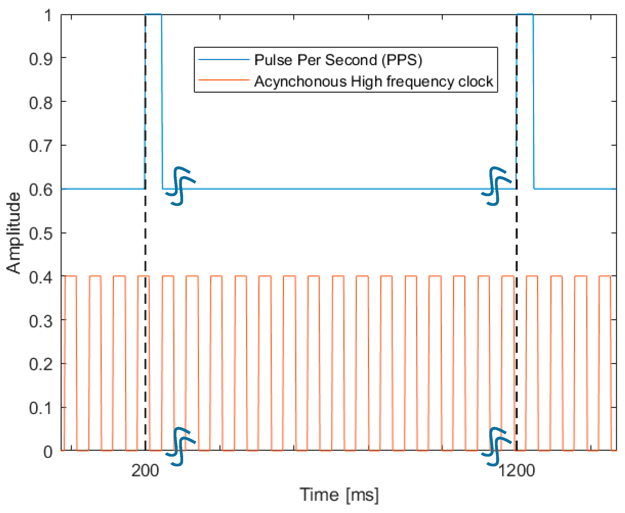
Figure 7.
Example of an asynchronous high frequency clock.

Figure 8.
Measured synchronization accuracy.

Figure 9.
Resampling of voltage signal; actual samples are interpolated in desired instants of time.
Figure 9.
Resampling of voltage signal; actual samples are interpolated in desired instants of time.


Table 1.
Maximum measured (Meas.) TVE, FE and RFE, and the corresponding limit values, in various testing conditions reported in IEEE Standards for Class P PMUs. The reported results refer to observation intervals of four nominal cycles and reporting rate of 50 fps.
Table 1.
Maximum measured (Meas.) TVE, FE and RFE, and the corresponding limit values, in various testing conditions reported in IEEE Standards for Class P PMUs. The reported results refer to observation intervals of four nominal cycles and reporting rate of 50 fps.
| Test Type | TVE max [%] | FE max [mHz] | RFE max [Hz/s] | |||
|---|---|---|---|---|---|---|
| Limit | Meas. | Limit | Meas. | Limit | Meas. | |
| Frequency offset (±2 Hz) | 1 | 0.11 | 5 | 1.0 | 0.4 | 0.13 |
| Frequency offset (±2 Hz) | 1 | 0.19 | 5 | 4.7 | 0.4 | 0.19 |
| +1% 2nd harmonic | ||||||
| Frequency offset (±2 Hz) | 1 | 0.15 | 5 | 1.1 | 0.4 | 0.15 |
| +1% 3rd harmonic | ||||||
| Frequency ramp | 1 | 0.35 | 10 | 7.7 | 0.4 | 0.19 |
| (±2 Hz at 1 Hz/s) | ||||||
| AM (10% at 2 Hz) | 3 | 1.8 | 60 | 27.0 | 2.3 | 2.1 |
| PM (0.1 rad at 2 Hz) | 3 | 1.4 | 60 | 45.0 | 2.3 | 1.5 |
Table 2.
Maximum measured (Meas.) TVE, FE and RFE, and the corresponding limit values, in various testing conditions reported in IEEE Standards for Class M PMUs. The reported results refer to observation intervals of four nominal cycles and reporting rate of 50 fps.
Table 2.
Maximum measured (Meas.) TVE, FE and RFE, and the corresponding limit values, in various testing conditions reported in IEEE Standards for Class M PMUs. The reported results refer to observation intervals of four nominal cycles and reporting rate of 50 fps.
| Test Type | TVE max [%] | FE max [mHz] | RFE max [Hz/s] | |||
|---|---|---|---|---|---|---|
| Limit | Meas. | Limit | Meas. | Limit | Meas. | |
| Frequency offset (±5 Hz) | 1 | 0.21 | 5 | 1.0 | 0.1 | 0.14 |
| Frequency offset (±5 Hz) | 1 | 0.22 | 25 | 9.5 | - | 0.45 |
| +1% 2nd harmonic | ||||||
| Frequency offset (±5 Hz) | 1 | 0.21 | 25 | 1.2 | - | 0.16 |
| +1% 3rd harmonic | ||||||
| Frequency ramp | 1 | 0.44 | 10 | 8.7 | 0.2 | 0.21 |
| (±5 Hz at 1 Hz/s) | ||||||
| AM (10% at 5 Hz) | 3 | 2.3 | 300 | 153.0 | 14 | 12 |
| PM (0.1 rad at 5 Hz) | 3 | 2.5 | 300 | 253.0 | 14 | 14 |
| 10% out-of-band inter-harmonic @ ≈ 25 Hz | 1.3 | 2.7 | 10 | 854.0 | - | 45 |
© 2019 by the authors. Licensee MDPI, Basel, Switzerland. This article is an open access article distributed under the terms and conditions of the Creative Commons Attribution (CC BY) license (http://creativecommons.org/licenses/by/4.0/).
Share and Cite
MDPI and ACS Style
Delle Femine, A.; Gallo, D.; Landi, C.; Luiso, M. The Design of a Low Cost Phasor Measurement Unit. Energies 2019, 12, 2648. https://doi.org/10.3390/en12142648
AMA Style
Delle Femine A, Gallo D, Landi C, Luiso M. The Design of a Low Cost Phasor Measurement Unit. Energies. 2019; 12(14):2648. https://doi.org/10.3390/en12142648
Chicago/Turabian StyleDelle Femine, Antonio, Daniele Gallo, Carmine Landi, and Mario Luiso. 2019. "The Design of a Low Cost Phasor Measurement Unit" Energies 12, no. 14: 2648. https://doi.org/10.3390/en12142648
Note that from the first issue of 2016, this journal uses article numbers instead of page numbers. See further details here.