1. Introduction
In recent years, multilevel inverters have become popular because of their competence for carrying high power, high voltage, good power quality, lower order harmonics, lower switching losses, and lower electromagnetic interference, due to the absence of an inductor and a capacitor [
1,
2,
3]. Multilevel inverters generate close to sinusoidal voltages, as in the form of a stepped voltage waveform, using many direct current (DC) voltage sources. In a multilevel inverter, increasing the number of output voltage levels results in lower THD at the output voltage. There are three kinds of multilevel inverter structures: diode-clamped, flying capacitor, and cascaded H-Bridge (CHB). To produce higher levels, the flying capacitor and diode-clamped topologies use many capacitors and diodes, respectively. Also, both of the structures suffer from voltage inequality of capacitors [
4,
5,
6,
7,
8]. The CHB topology can be suitable to generate higher voltage levels, because it requires fewer components compared to the conventional topologies [
1,
2]. CHB inverters can increase the number of output voltage levels by increasing the number of H-Bridges used, which increases the number of switching devices used; this makes a multilevel inverter more complicated. Modifications to the H-Bridge inverter topology reduces the number of components. A bi-directional switch is added in the conventional H-Bridge to get two additional voltage levels via a capacitor from a single DC voltage source, and final output is a stepped five-level output voltage [
9,
10,
11,
12,
13,
14]. A series and parallel connection of DC voltage sources cascaded with a conventional H-Bridge gives a stepped output with the reduced harmonics content in the output voltage [
15,
16]. Series connections of sub-multilevel, half-bridge symmetrical and asymmetrical inverters generate 13 and 31 levels, respectively, when cascaded to an H-Bridge inverter, in this topology six switches are “ON” in all the modes of operation [
17,
18]. Two half-bridges are cascaded by adding two unidirectional switches, and this forms the seven-level inverter [
19]. The cascading of two units of developed H-Bridges produces 49 output voltage levels, but in all the modes of operation, six switches are in the “ON” state [
20]. Two cascaded half H-Bridges are nested to form a single unit. One half-bridge inverter and two units of the nested cascaded half H-Bridges are connected in series with the H-Bridge inverter to generate 15 levels, and comprised of 16 switches and seven DC sources. In this topology, a minimum of five switches and a maximum of nine switches are in the “ON” state [
21]. Most of the inverters use pulse width modulation method to generate the switching pulses; due to this, the switching losses are very high, especially in high-voltage and high-power multilevel inverters. Frequent high-voltage switching generates more heat, due to power losses in the switches, so reference frequency switching is best to minimize the switching losses [
22]. A new multilevel inverter based on modified H-Bridge topology generates a 13-level stepped output, and uses the capacitor to generate the in-between levels, but voltage balancing of the capacitor is difficult and bulky under various loaded conditions [
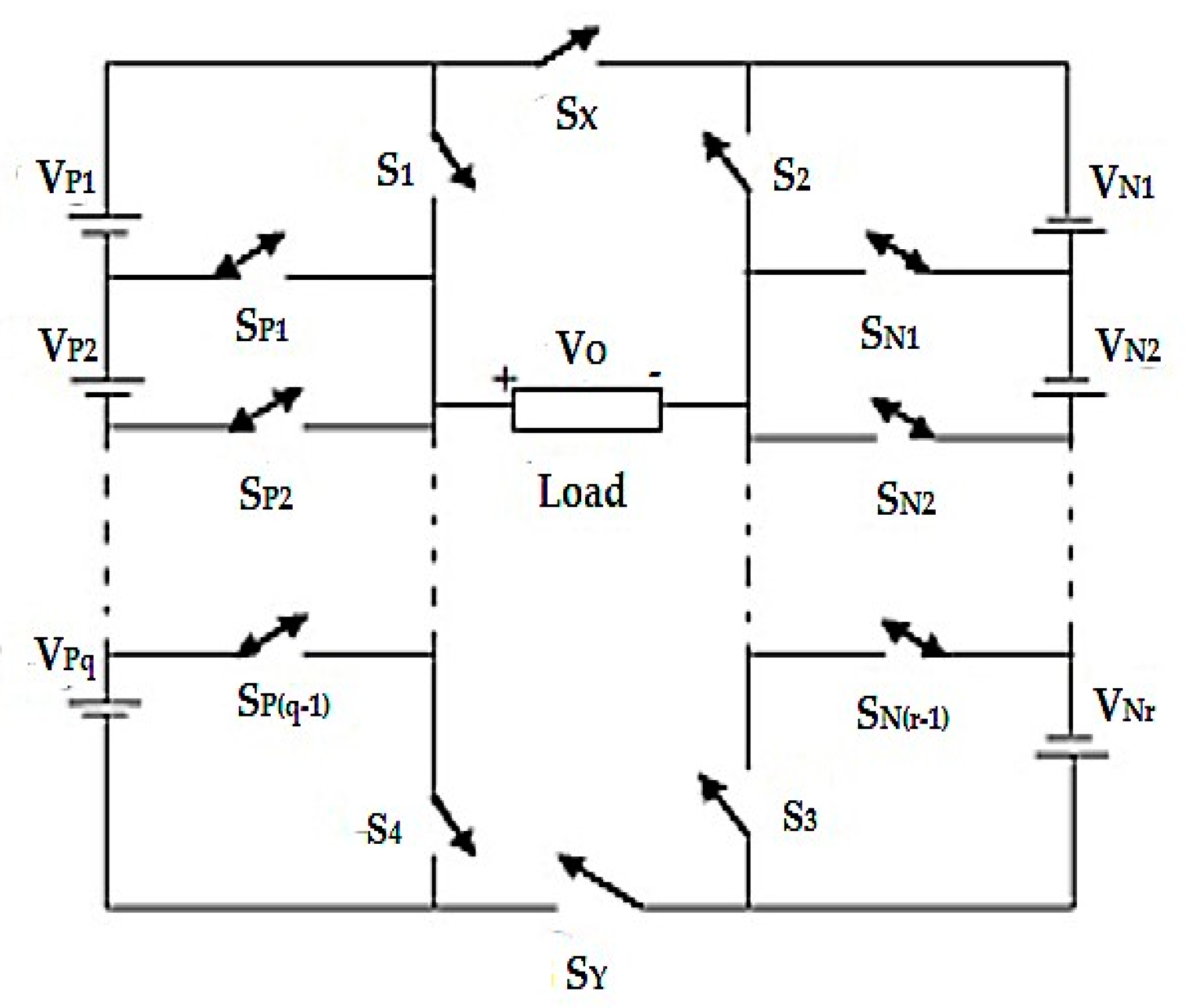
23]. The proposed topology consists of a left-side half H-Bridge inverter with
q number of DC sources, (q − 1) number of bidirectional switches, and similarly the right-side half H-Bridge inverter with
r number of DC sources, (r − 1) number of bidirectional switches. Finally, these two half H-Bridges cascaded with two unidirectional (S
X, S
Y) switches, as shown in
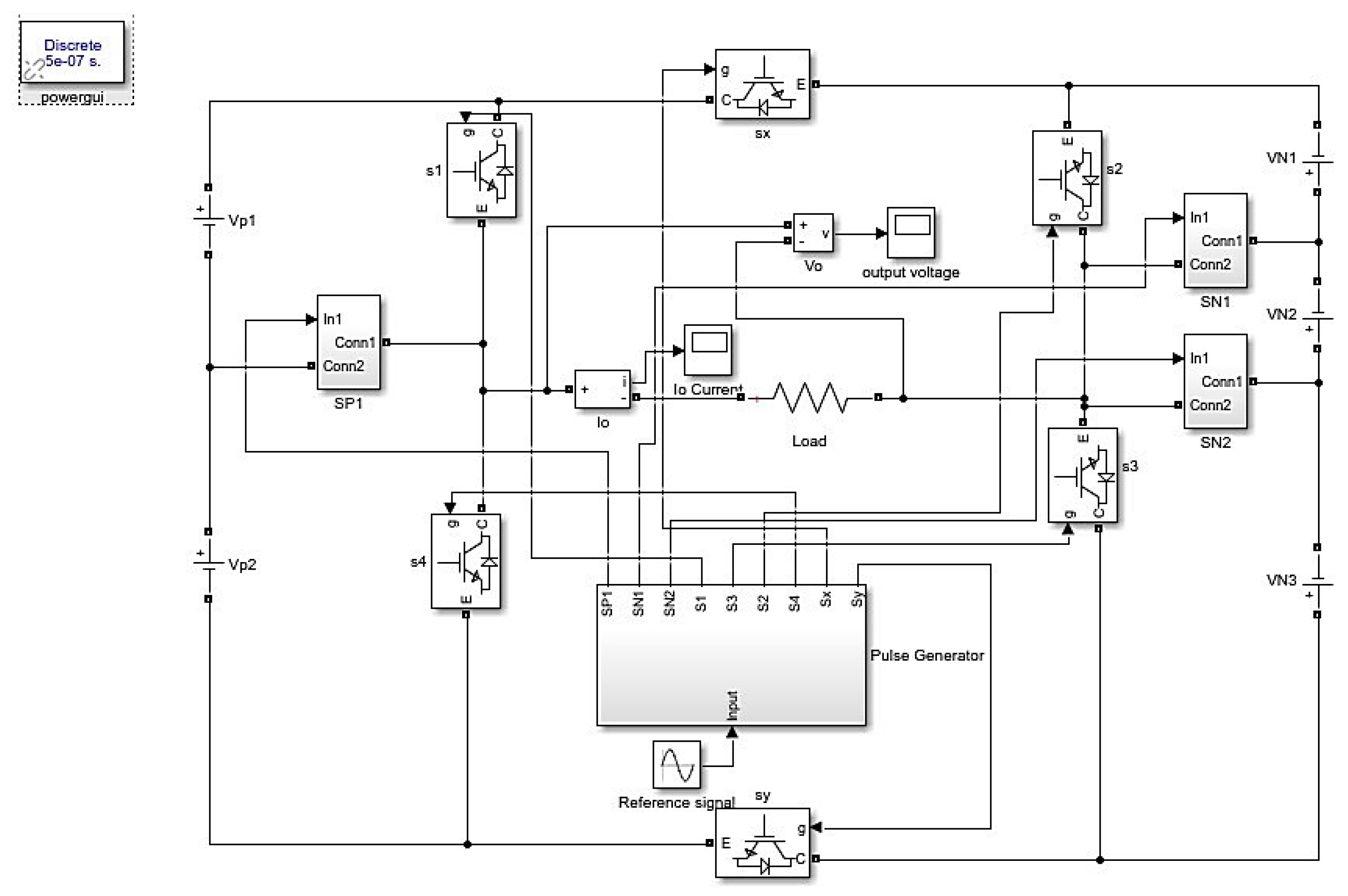
Figure 1. In the proposed enhanced H-Bridge (EHB) multilevel inverter (MLI), in all the modes of operation, only three switches are “ON”, and a reference frequency switching method is used so that the conduction losses and switching losses are minimal. In this proposed topology, there is no storage element like an inductor, and hence the losses are minimized. In this paper, to enhance the performance of the base unit and to reduce the THD, a choice of bidirectional switches and DC sources on both sides with two different methods and a sinusoidal tracking algorithm is proposed, with simulated and experimental results. This EHB MLI is suitable for medium-voltage applications and also used in v/f control drives.
3. DC Voltage Source Selection Methods
The general enhanced H-Bridge consists of (q - 1) bi-directional switches (S
P1, S
P2, S
P3…S
P(q−1)) on the left side, (r − 1) bi-directional switches (S
N1, S
N2, S
N3…S
N(r−1)) on the right side, and six unidirectional power switches, (S
1, S
2, S
3, S
4, S
X, and S
Y) are available in the developed H-Bridge inverter. The proposed topology as shown in
Figure 1 contains q number of voltage sources (V
P1, V
P2, V
P3…V
Pq) and r number of voltage sources (V
N1, V
N2, V
N3…V
Nr) in the left and right side, respectively. Based on the relationship between left- and right-side voltage sources, two methods are proposed here.
Method I
There are
q number of voltage sources (V
P1, V
P2, V
P3…V
Pq) in the left side, and are equal in magnitude.
where q = 1, 2, 3…C
There are
r number of voltage sources (V
N1, V
N2, V
N3…V
Nr) in the right side, and are equal in magnitude.
where r = 1, 2, 3…D
Equations (3) and (4) specify the difference in magnitude between the left and right side voltage sources when Method I is applied.
Equations (7) and (8) specify the difference in magnitude between the left and right side voltage sources when method II is applied.
Method I Example
In SSEHB, the equal number of bidirectional switches on both sides is
In the SSEHB topology, the number of output voltage levels (N
Level) is
If n = 1, .
If n = 2, .
The number of uni-directional switches is
The number of bi-directional switches is
The number of dc voltage sources
The maximum and minimum magnitude of the generated output voltage is
if the number of bidirectional switches are not equal on both side, then
If
Else if
In the ASEHB topology, the number of output voltage levels (N
Level) is
If n = 1 and x = 0, then .
If n = 1 and x = 1, then .
If n = 1 and x = 2, then
.
Method II Example
Where n is an equal number of bidirectional switches on both sides (SSEHB). The value of n can be found by using Equation (9).
The number of levels in the inverter output voltage is given below:
If n = 1, then .
If n = 2, then .
If n = 3, then .
The equations for the number of uni-directional switches (NUni), number of bi-directional switches (NBi), number of dc voltage sources (NDC), maximum magnitude of the generated output voltage (VO,Max), and the minimum magnitude of the generated output voltage (VO,Min) are the same for the SSEHB topology represented in Equations (11)–(15), respectively.
If the topology contains unequal bidirectional switches (ASEHB) i.e., (q − 1) bi-directional switches at the left side and (r − 1) bi-directional switches at the right side. The value of n and x can be found by using Equations (17) and (18), respectively.
If n = 1, x = 0, then .
If n = 1, x = 1, then .
If n = 3, x = 5, then .
The equations for the number of uni-directional switches (NUni), number of bi-directional switches (NBi), number of DC voltage sources (NDC), maximum magnitude of the generated output voltage (VO,Max), and the minimum magnitude of the generated output voltage (VO,Min) are the same for the ASEHB topology represented in Equations (20)–(24) respectively.
In this section, a various number of bidirectional switches are associated with the developed H-Bridge to enhance the performance of the base unit SSEHB and ASEHB inverter, and for further enhancement, the various methods are applied to the proposed inverters, as shown in
Figure 1. The number of output voltage levels for the different number of bidirectional switches and the two methods are tabulated in
Table 1.
From
Table 1, one can choose the number of bidirectional switches needed for the required level of output voltage. Comparing Methods I and II, Method II gives more output voltage levels for the same number of bidirectional switches.
3.1. Modes of Operation
As shown in
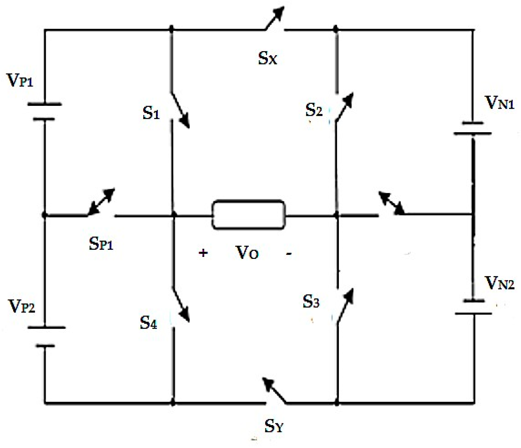
Table 2, the SSEHB multilevel inverter shown in
Figure 2 can generate 13 voltage levels—(±V
P2), ±(V
P1 + V
P2), ±(V
N2 + V
P2), ±(V
N2 + V
P2 + V
P1), ±(V
N2 + V
N1 + V
P2), ±(V
N2 + V
N1 + V
P2 + V
P1), and (0) at the output, by selecting different magnitudes of the DC voltage sources as per the proposed Method I. As per the proposed Method II, the same SSEHB inverter is able to generate 17 levels by selecting different magnitudes of the DC voltage sources.
The ASEHB multilevel inverter shown in
Figure 3 is able to generate 17 voltage levels.at the output by selecting different magnitudes of the DC voltage sources, as per the proposed method I. As per the proposed method II, the same ASEHB inverter is able to generate 23 levels by selecting different magnitudes of the DC voltage sources, as shown in
Table 3. The output voltage levels are ±(V
P2), ±(V
P1 + V
P2), ±(V
N3), ±(V
N3+ V
P2), ±(V
N3+ V
P2 + V
P1), ±(V
N3 + V
N2), ±(V
N3 + V
N2+ V
P2), ±(V
N3 + V
N2 + V
P2 + V
P1), ±(V
N3 + V
N2+ V
N1), ±(V
N3 + V
N2 + V
N1 + V
P2), ±(V
N3 + V
N2 + V
N1 + V
P2+ V
P1), and (0).
The 23 levels of the output voltage give 23 modes of operation. In any mode of operation, three switches are “ON”, and the remaining switches are “OFF”, as shown in
Table 3. In all the modes of operation, one switch from the left side inverter circuit (S
1, S
4, or S
P(q − 1)) and one switch from the right side inverter circuit (S
2, S
3, or S
N(r − 1)), and one switch from the cascade connection (S
X, S
Y) are always in the “ON” state.
3.2. Voltage Stress across Switches
An important parameter that determines the cost of a multilevel inverter is the blocking voltage of the power switches, as well as the DC voltage sources. If the proposed inverter requires a variety of blocking voltage switches, then the cost of the inverter is too high. The voltage blocking mainly depends on the topology of the inverter. In this section, voltage stress across various switches are derived for SSEHB and ASEHB inverters when methods I and II are applied. The equation to find the voltage stress across the switches is the same for both the SSEHB and ASEHB inverter.
The relation between VPq and VNr for Method I employing SSEHB and ASEHB inverters is shown in Equation (4). Similarly, the relationship between VPq and VNr for Method II employs SSEHB, and an ASEHB inverter is shown in Equation (8). For finding the blocking voltage across a switch substitute, the value of VNr in terms of VPq can be determined by Equations (27)–(31).
The blocking voltage across various power switches are given below:
3.3. Conduction and Switching Losses
In this proposed ASEHB MLI, in all the modes of operation, only three switches are “ON”, and corresponding driver circuits are only “ON”, and so the power loss in the inverter during conduction is less compared to cascaded conventional H-Bridge inverter—hence, the efficiency of the inverter is improved. Here P
C is the conduction loss of the power switches.
where I is the current following through the switch, and R
on is the on-state resistance of the switch during conduction period.
The switching losses mainly depend on the carrier frequency in pulse width modulation inverter, whereas here the switching is done based on the reference frequency compared with the input DC voltage levels, so the switching losses depend on the number of levels of the inverter. Here the switching losses are calculated in three group of switches.
The left side group is comprised of the switches S
1, S
4, and S
P1 to S
P(q − 1), and the total left-side group switch losses is equal to P
SL. Similarly, the right-side group is comprised of the following switches S
2, S
3, and S
N1 to S
N(r-1), and the total right-side group switch losses is equal to P
SR. Finally, the cascaded group comprises the following switches S
X and S
Y, and the total cascaded switching losses are equal to P
Scas.
Here the fref is the reference frequency, and Cce is the capacitance across the collector and emitter of IGBT.
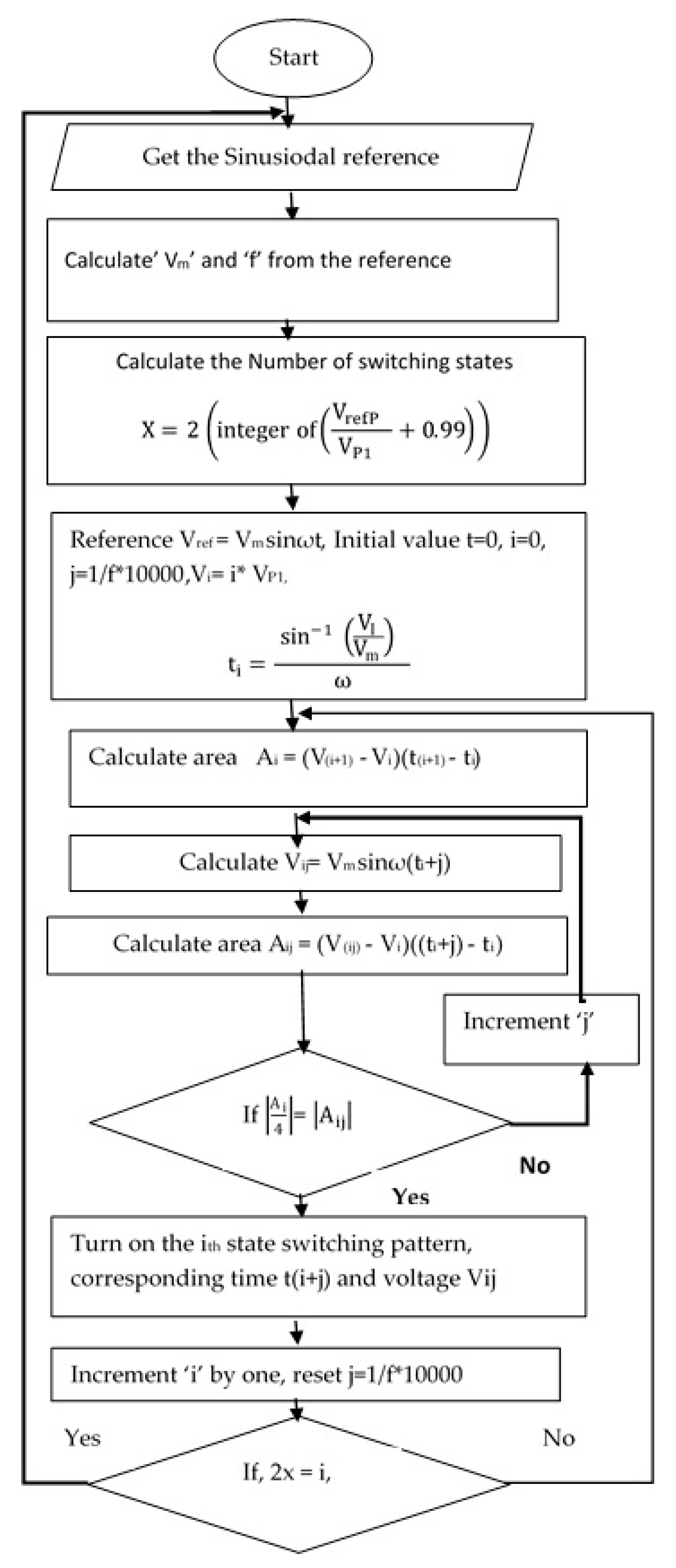
3.4. Sinusoidal Tracking Algorithm for an Enhanced H-Bridge Multilevel Inverter
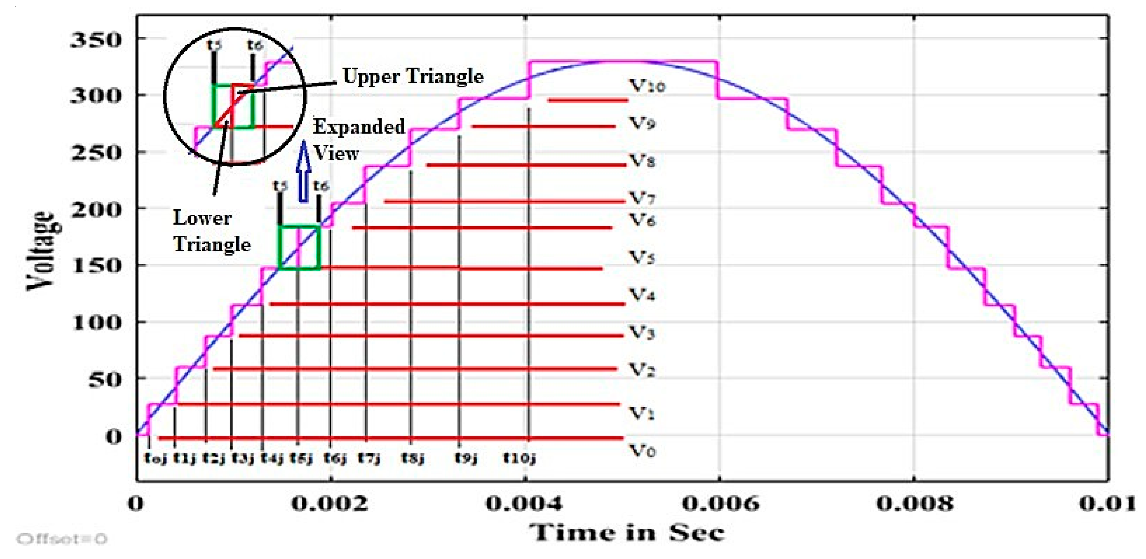
This algorithm tracks the fundamental sinusoidal function to calculate the time at which to turn on the switches. The V
m and f is calculated with the help of sinusoidal reference. With the help of f and V
m = V
ref.p, fundamental reference V
ref is generated as given in Equation (36). A rectangle with area A
i is formed between successive voltage levels (∆V), and the time interval between these voltage levels (
∆t). To find the equal area between two successive voltage levels, increment time by j, where the sampling time j is given in Equation (38). Increment the time by j and find V
ij, then calculate the area A
ij until the area of the rectangle is exactly 25% of the total area A
i. At that resultant time (t
jopt) or angle (
α) and voltage, the corresponding switches for i mode are turned on. Similarly, calculate for all the voltage levels from zero to V
max. The best switching times to get the minimum THD using this sinusoidal tracking method is the time when the areas of the upper and the lower triangle of the fundamental sinusoidal wave are equal, as shown in
Figure 4.
Figure 5 details the switching states and timing calculation of the sinusoidal tracking algorithm for various input sinusoidal reference using a flowchart. This sinusoidal tracking algorithm is implemented with the help of a high-level language. The switching time is calculated offline and stored in the local PROM (programmable read only memory) of the PIC (peripheral interface controller) for various inputs of sinusoidal reference. Consider that the input DC voltages are stable and ripple-free to get a perfect enhanced performance for the proposed EHB MLI.
3.5. Comparison with Other Multilevel Inverters
Table 4 compares the advantages of the proposed enhanced H-Bridge MLI with the various other H-Bridge multilevel inverters. N
ON is the number of switches that are “ON” in a particular state.
The modified H-Bridge inverter [
7] requires 14 bidirectional switches and 15 symmetrical value DC voltage sources to get a 31-level output voltage. The cascaded developed H-Bridge inverter [
19] needs 10 unidirectional switches and four DC voltage sources to get a 31-level output voltage. With the proposed base unit EHB 31 level inverter, or even a 99-level inverter, in all the modes of operation only three switches are “ON”, whereas with the cascaded developed H-Bridge [
19], five switches are on in all the modes of operation for 31 levels. Hence, the switching conduction losses are minimized compared to the cascaded developed H-Bridge [
19], but there is an increase in the number of DC sources. The proposed enhanced H-Bridge is the most suitable for a higher number of levels, a lower THD with reduced switching conduction losses, and the lesser number of a variety of blocking voltage power switches.
4. Simulation Results
To study and verify the performance of a single-phase SSEHB 13-level inverter with optimum components, a 13-level output based on the Method I has been simulated.
Table 2 shows the switching states of the 13-level inverter. Simulation has been done by using MATLAB/SIMULINK R2017a software, and
Table 5 lists the simulation parameters. For the proposed SSEHB 13-level inverter, the output voltage is obtained by comparing various (±55, ±110, 165, ±220, ±275, ±330, 0) DC levels with the fundamental sinusoidal function (335 V), as per the switching pattern, is given in
Table 2. Similarly, to study and verify the performance of a single-phase ASEHB 23-level inverter with optimum components, a 23-level output voltage based on Method II has been simulated.
Table 3 shows the switching states of the 23-level inverter. The output voltage of the proposed ASEHB 23-level inverter is obtained by comparing the various (±30, ±60, ±90, ±120, ±150, ±180, ±210, ±240, ±270, ±300, ±330, 0) DC levels with the fundamental sinusoidal function (335 V) as per the switching pattern given in the
Table 5.
The MATLAB/SIMULINK model for the proposed ASEHB 23-level inverter 300 V peak is as shown in
Figure 6.
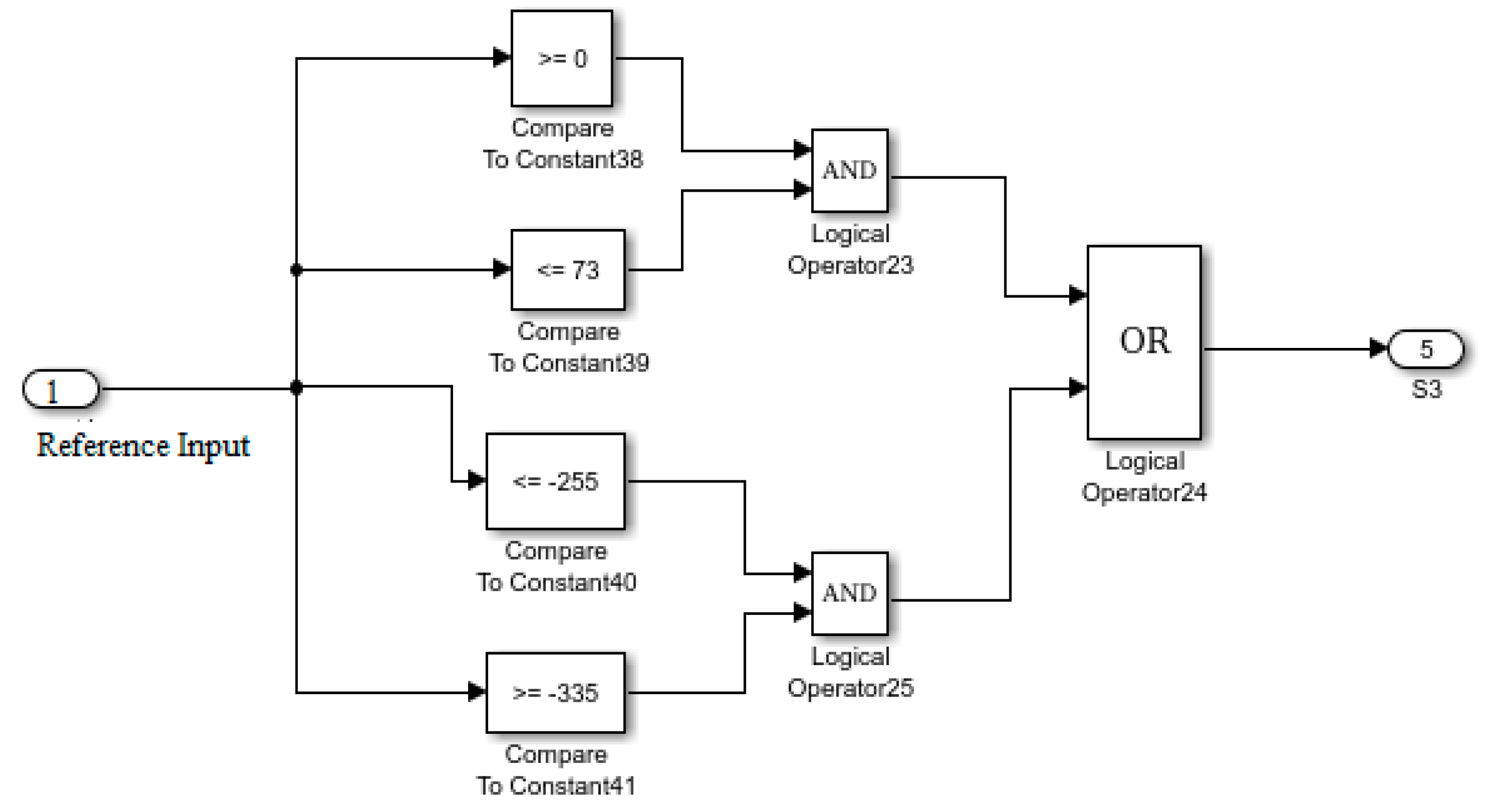
The pulse generator of switch S
3 is shown in
Figure 7. The optimum time (t
jopt) to turn on a switch is obtained from the sinusoidal tracking algorithm. The amplitude of the reference sinusoidal at the optimum time (t
jopt) and the previous state of a switch is compared to generate the pulse. Similarly, for all the transitions of switch S
3, switching pulses are generated and logically ‘OR’ed to give the complete pulse of S
3. The switching pulses for all other switches are generated using the same procedure.
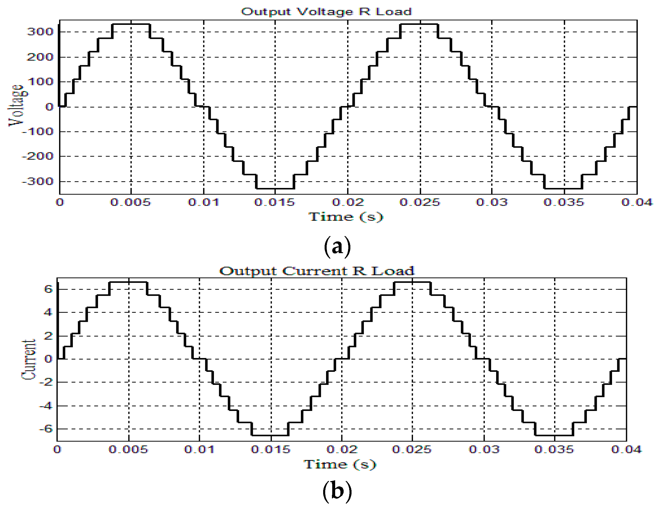
Figure 8 shows the simulated output voltage and current waveforms of a proposed single-phase SSEHB 13-level inverter connected to a standalone R load. From observation, the SSEHB inverter generates the desired 13-level, 50 Hz stepped output voltage (sinusoidal fundamental) and the current waveform.
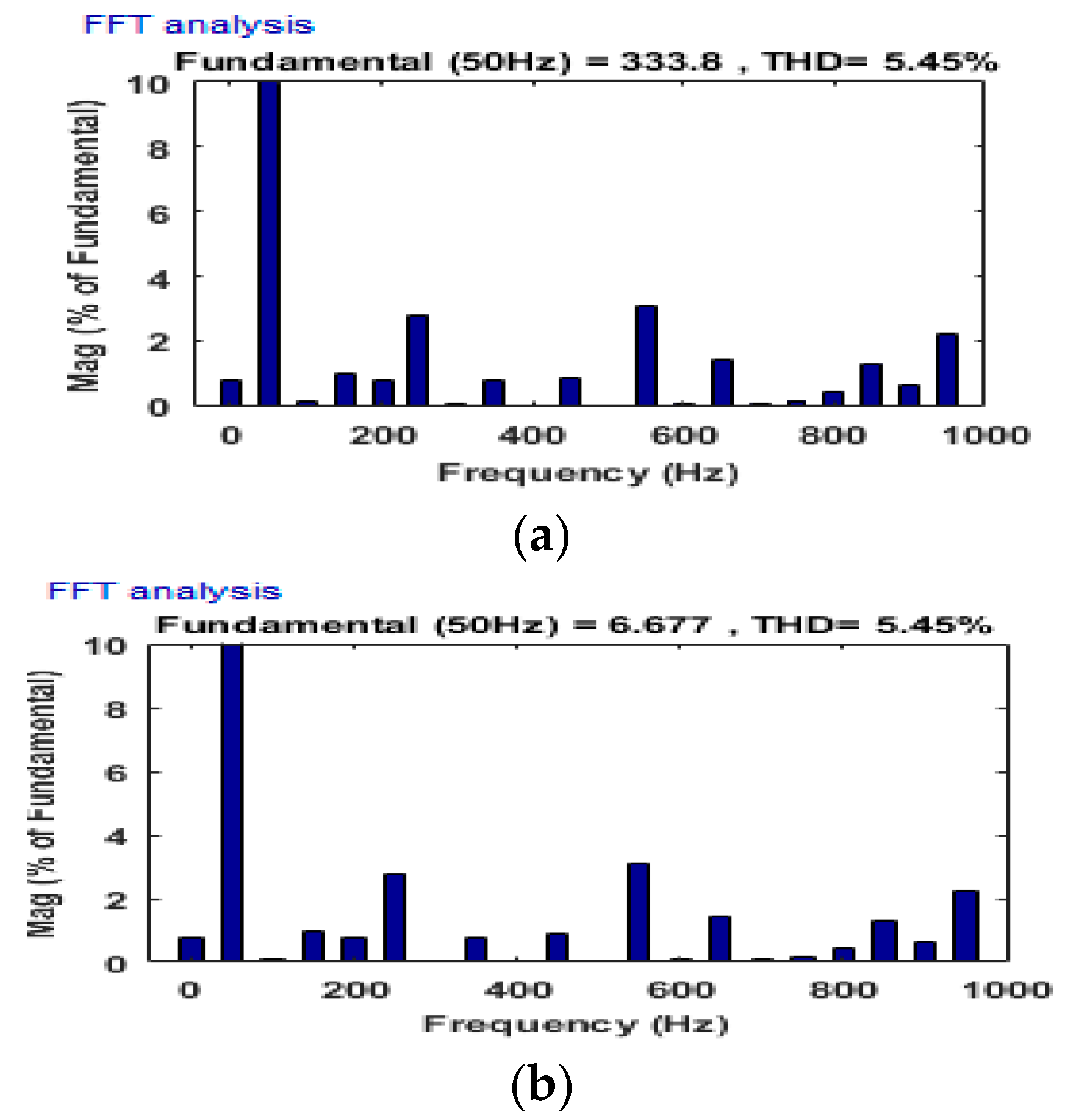
Figure 9 Shows the frequency spectrum of the SSEHB 13-level inverter’s output voltage and current waveform when connected to a purely resistive load. The total harmonic distortion of voltage and current is found to be 5.45% and 5.45%, respectively.
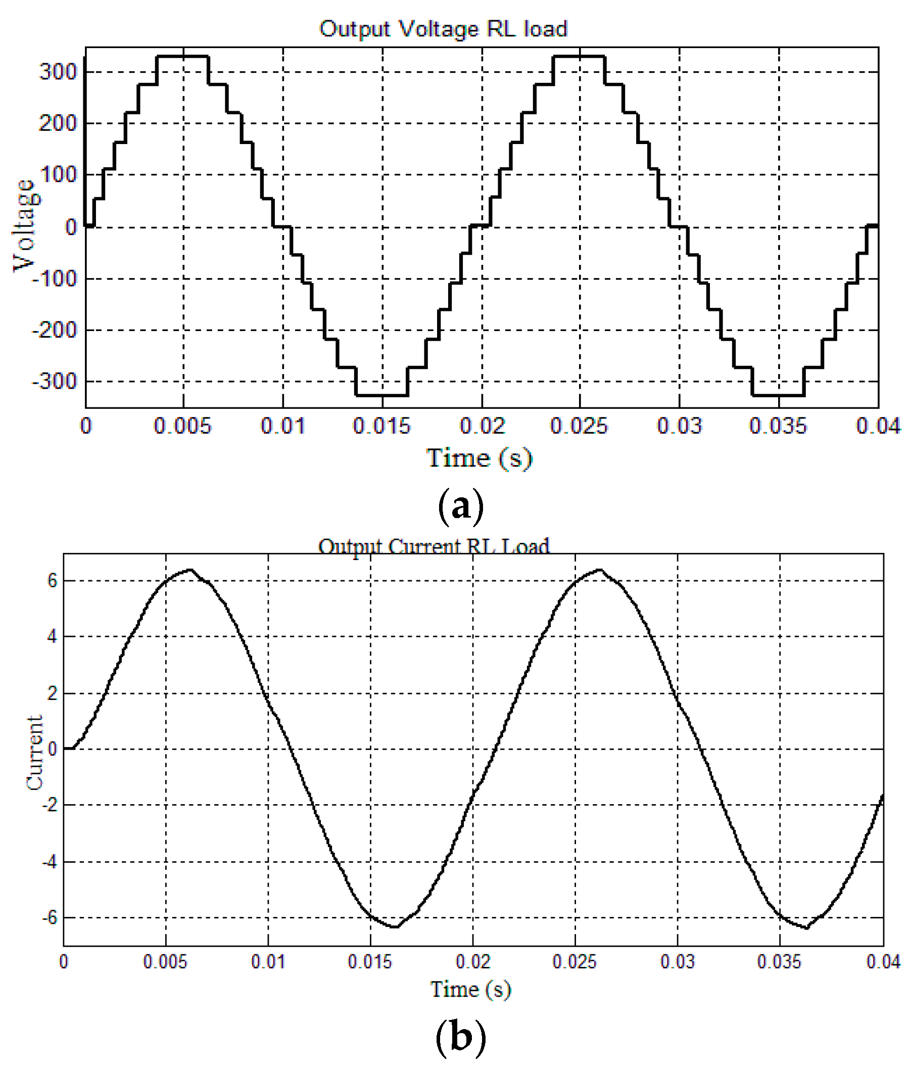
Figure 10 shows the simulated output voltage and current waveforms of a proposed single phase SSEHB 13-level inverter connected to a standalone RL load. From the observation, the SSEHB inverter generates the desired 13-level, 50 Hz stepped output voltage (sinusoidal fundamental) and the current waveform.
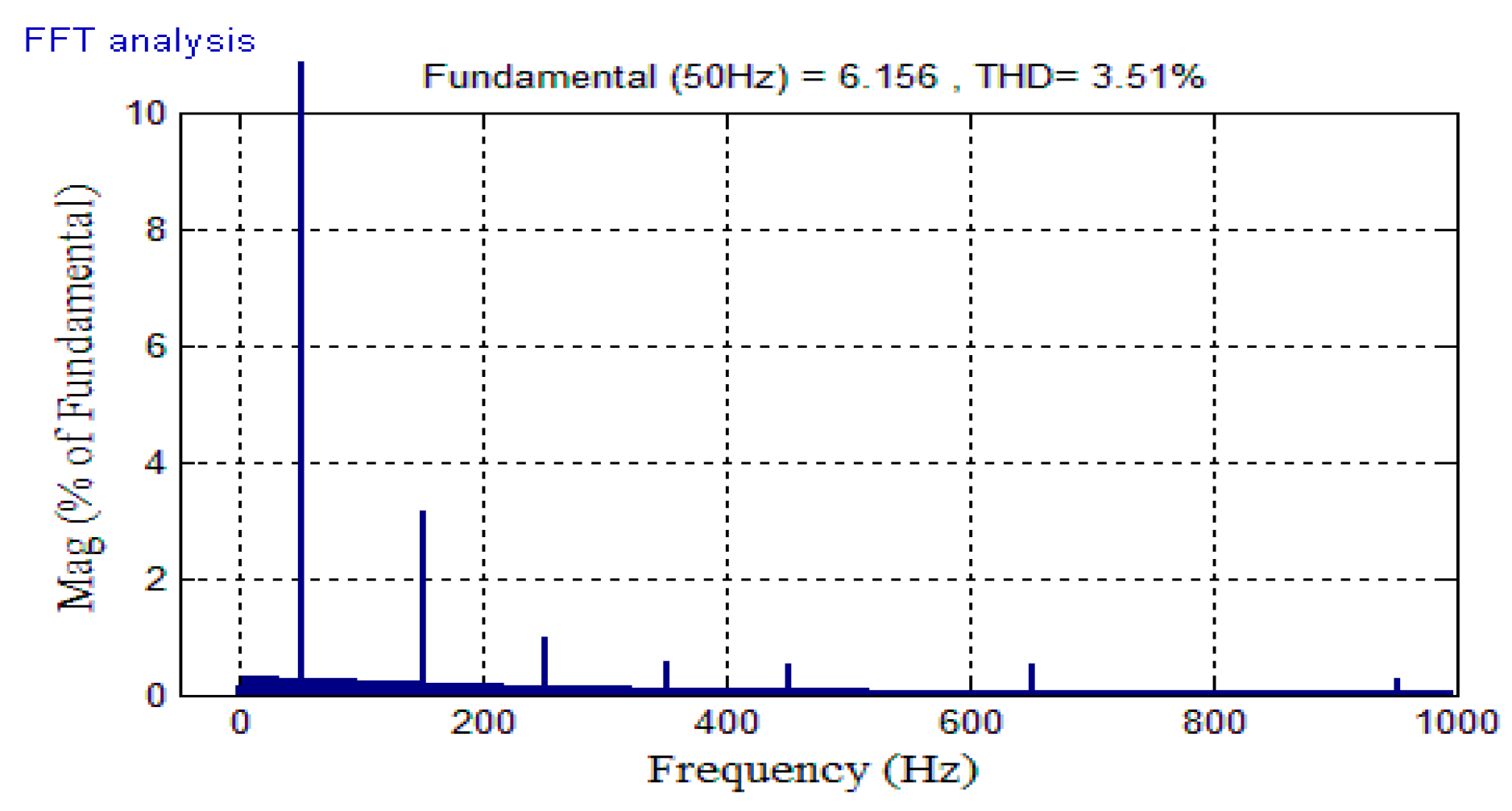
Figure 11 shows the frequency spectrum of the SSEHB 13-level inverter’s output voltage and current waveform when connected to an RL load. The total harmonic distortion of the current is found to be 3.51%.
Figure 12 shows the simulated output voltage and current waveforms of a proposed single-phase ASEHB 23-level inverter connected to a standalone R load. From observation, the ASEHB inverter generates the desired 23-level, 50 Hz stepped output voltage (sinusoidal fundamental) and the current waveform.
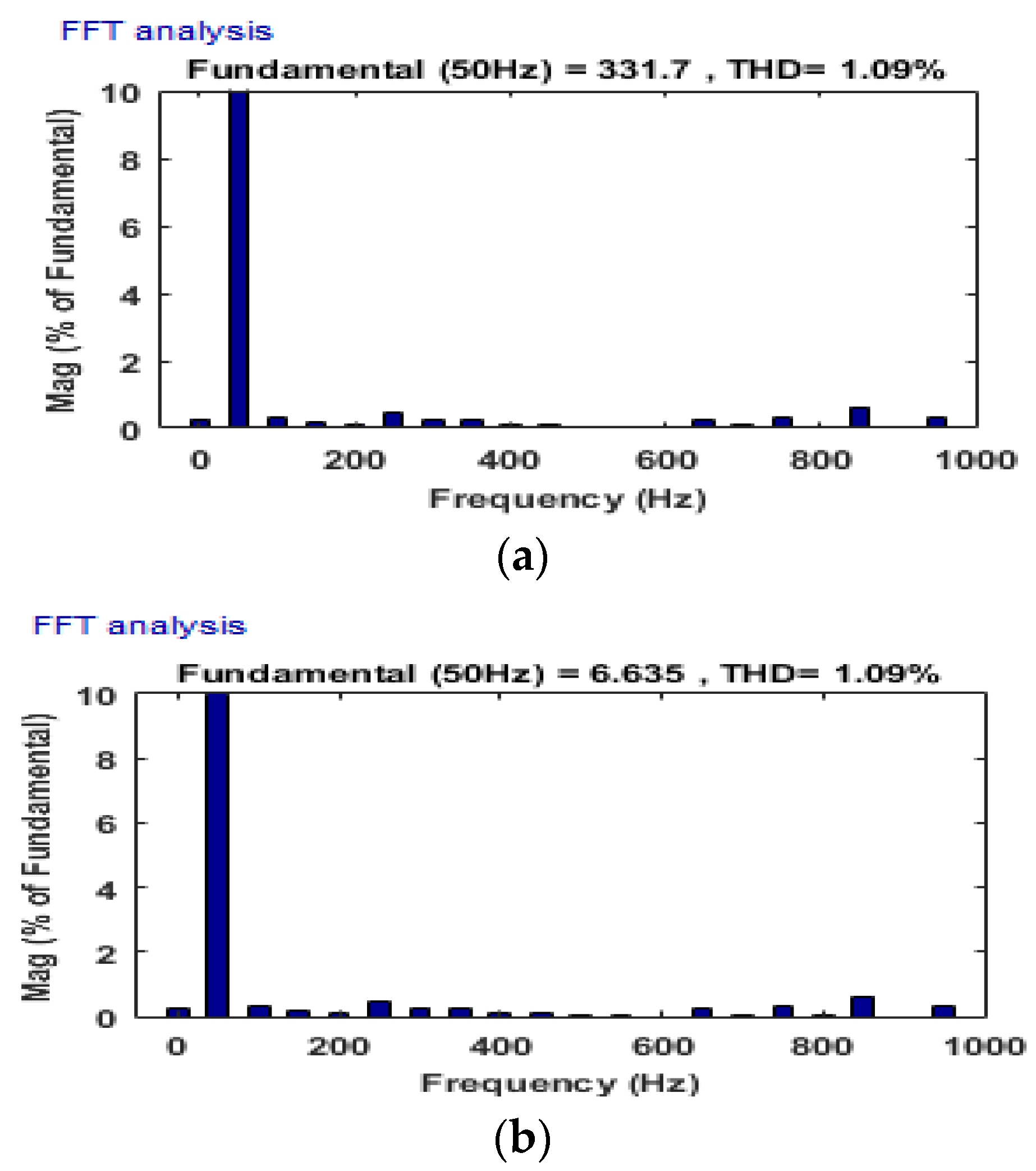
Figure 13 shows the frequency spectrum of the ASEHB 23-level inverter’s output voltage and current waveform when connected to a purely resistive load. The total harmonic distortion of voltage and current is found to be 1.09% and 1.09%, respectively.
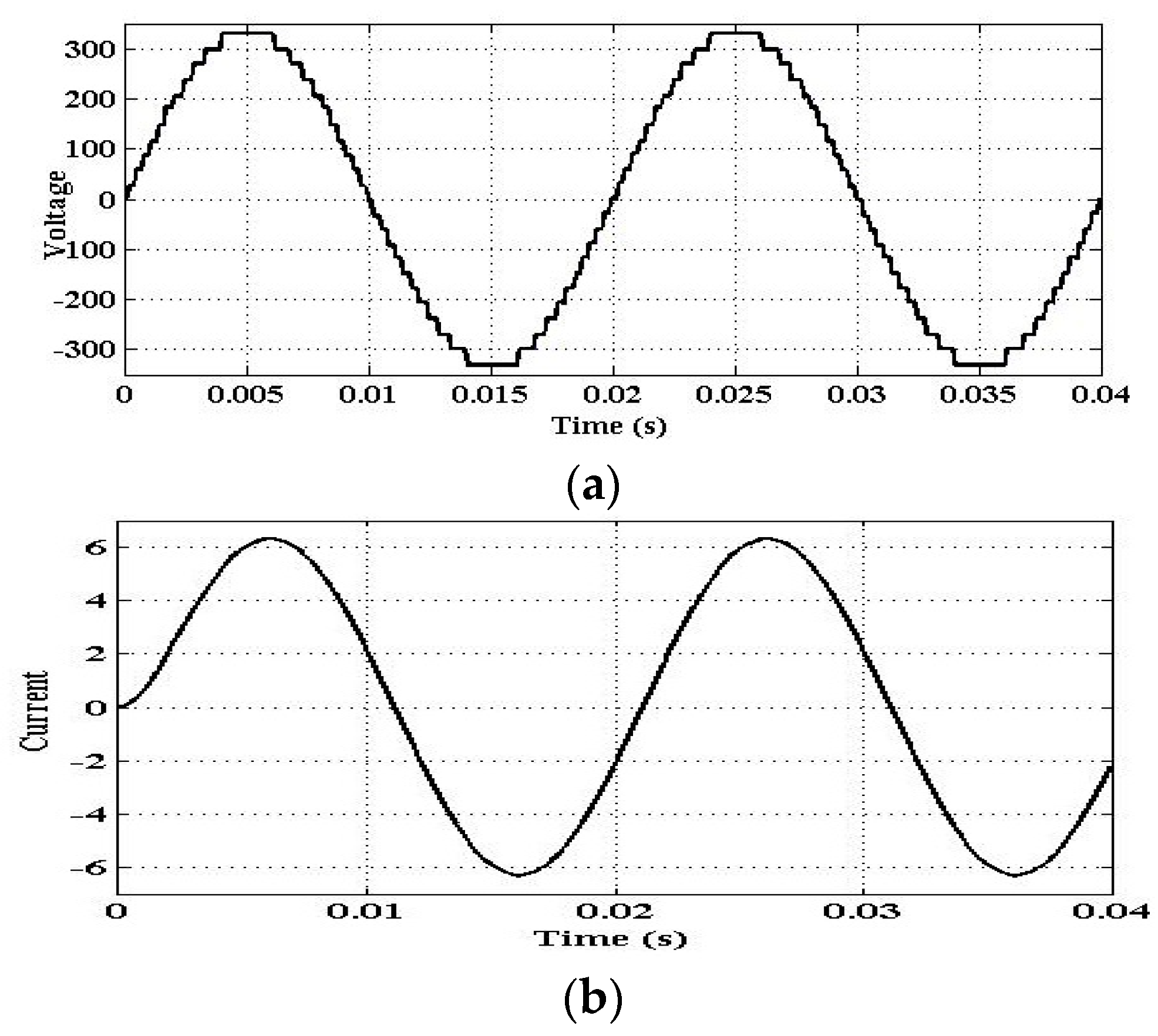
Figure 14 shows the simulated output voltage and current waveforms of a proposed single-phase ASEHB 23-level inverter connected to a standalone RL load. From the observation, the ASEHB inverter generates the desired 23-level, 50 Hz stepped output voltage (sinusoidal fundamental) and the current waveform.
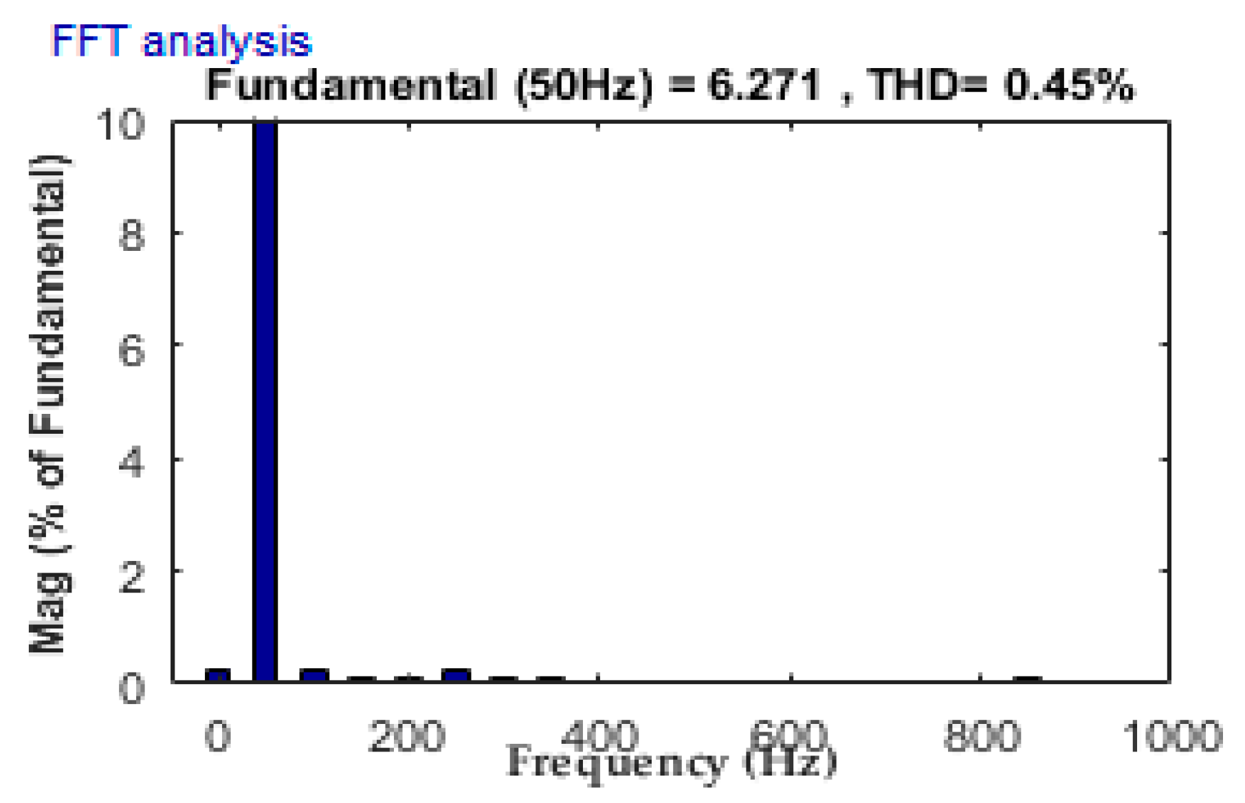
Figure 15 shows the frequency spectrum of the ASEHB 23-level inverter’s output current waveform when connected to an RL load. The total harmonic distortion of current is found to be 0.45%.
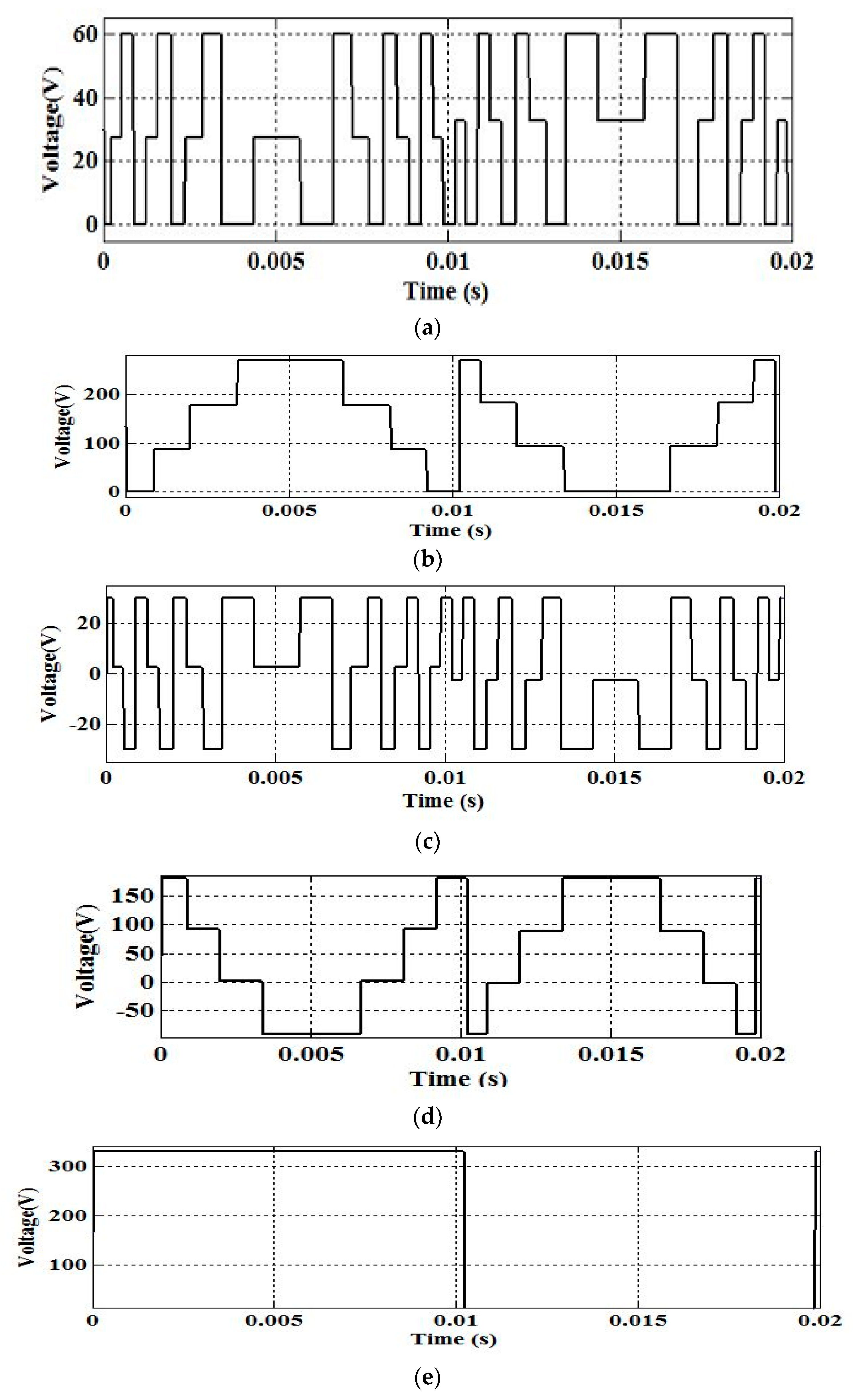
The voltage stress across the various switches of an ASEHB 23-level 330 V peak inverter with the help of MATLAB simulation is shown in
Figure 16. Analyzing
Figure 16, the maximum voltage stress across the switches is S
1 = 60 V, S
2 = 270 V, S
P1 = 30, S
N1 = 180, and S
X = 330, which is validated with Equations (27)–(31), respectively.
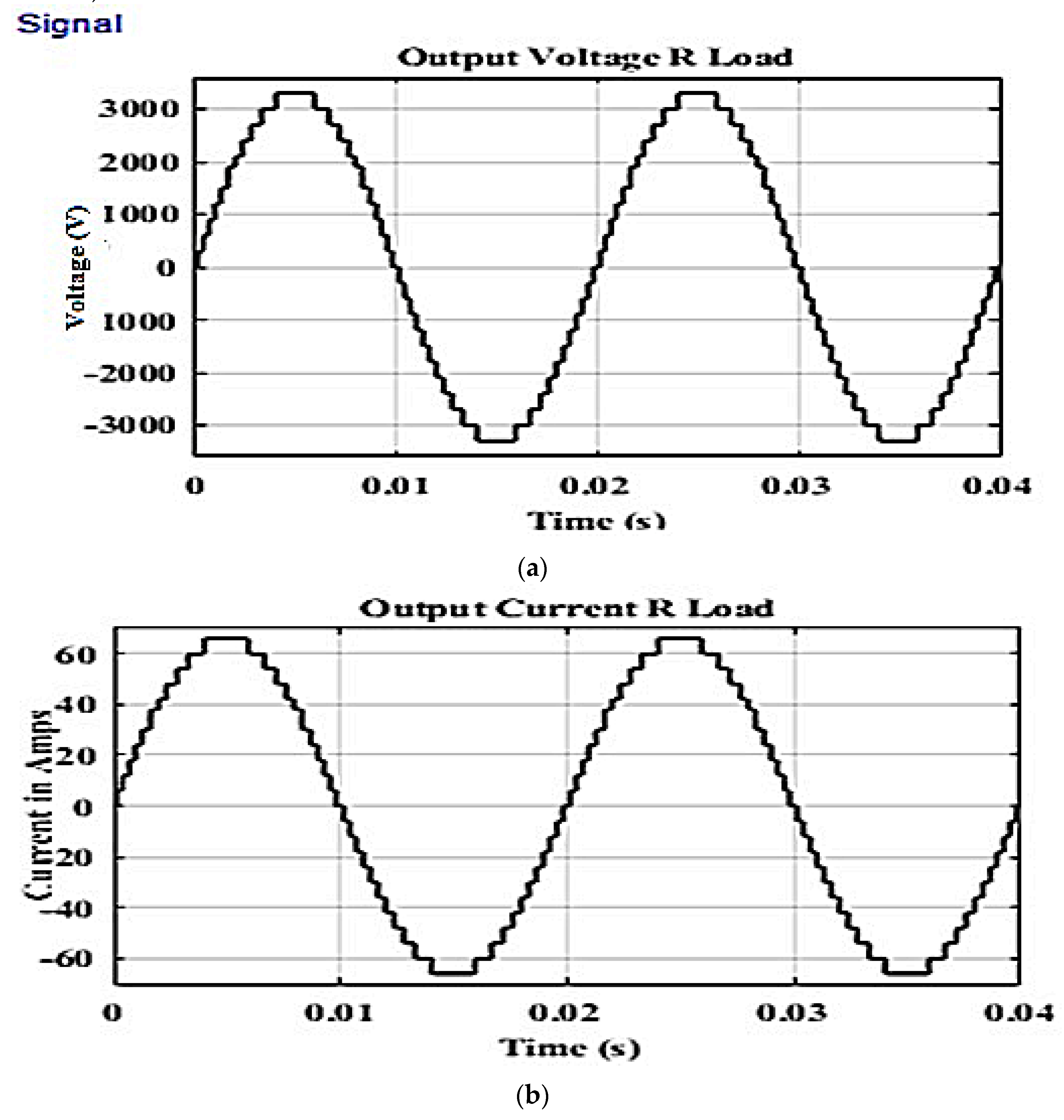
Figure 17 shows the simulated medium output voltage and current waveforms of a proposed single-phase ASEHB 23-level inverter connected to a standalone R load. From the observation, the ASEHB inverter generates the desired 23-level, 50 Hz stepped peak 3300 V output voltage (sinusoidal fundamental) and the current waveform.
Figure 18 shows the frequency spectrum of the ASEHB 23-level inverter’s output 3300 V peak waveform when connected to an R load. The total harmonic distortion of the voltage was found to be 1.09%.
Experimental Results
From
Table 3, an ASEHB inverter employed with Method II produces a higher number of output voltage levels compared to Method I for the same number of switching devices. The complete comparison is also tabulated in
Table 1. This comparison, along with the simulation results shown in
Figure 12a, has been the motivating factor in developing an ASEHB 23-level inverter working model.
Table 6 lists the hardware specifications. In this, the PIC 16F887 series is used to generate the switching states, with the help of a comparison of various DC voltage levels with the reference signal, and stores the switching state’s timing in it.
The switching frequency is very low, as per the comparison of various DC voltage levels with the reference signal; hence, IGBT was chosen for power inverter circuits. This switching pulse triggers the IGBT switches present in the inverter through isolated gate driver circuits.
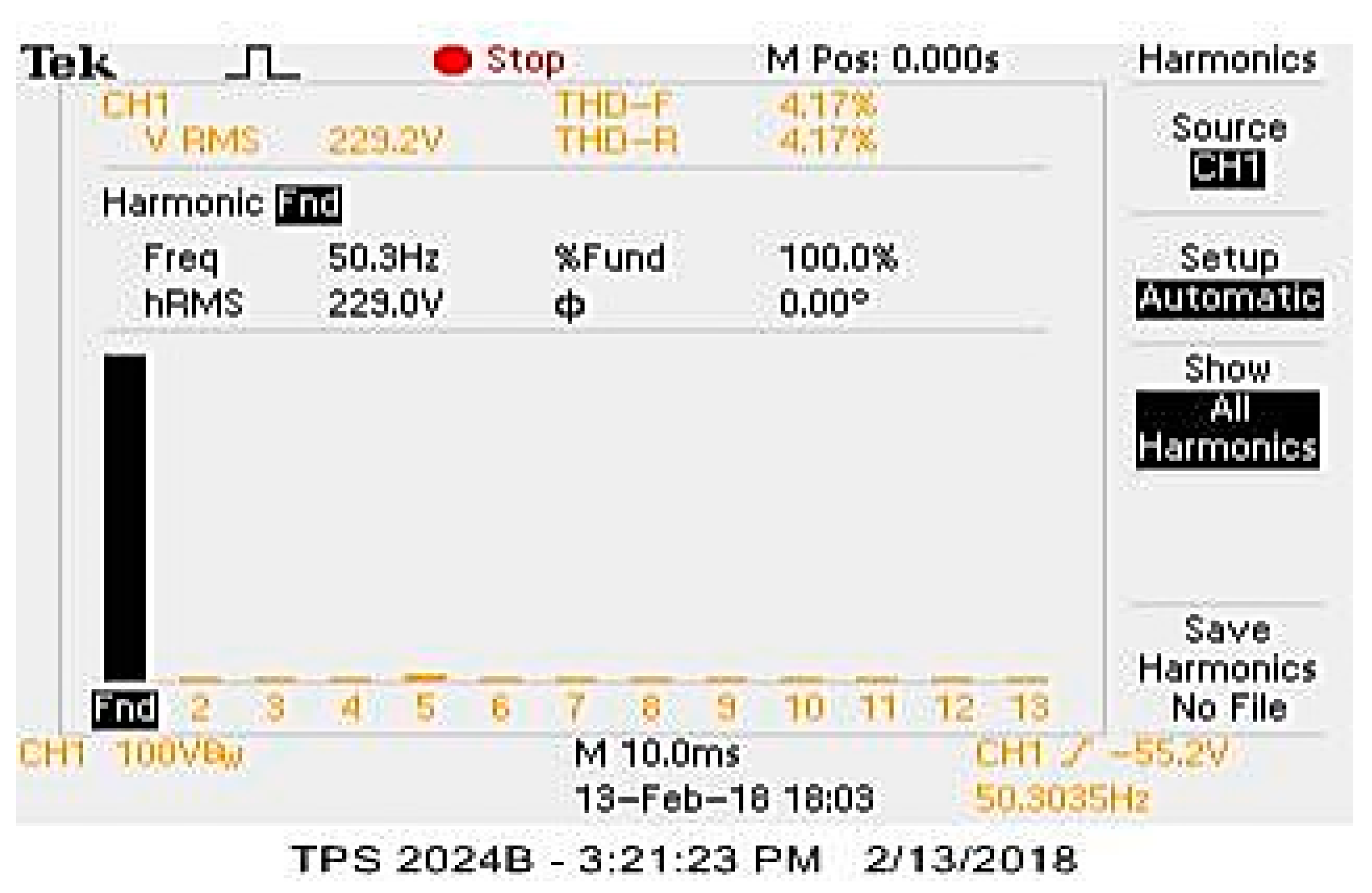
Figure 19 shows the hardware layout, and the ASEHB 23-level 660 V peak-to-peak and 233 V RMS (root mean square) hardware output voltage is shown in
Figure 20. The THD value of an ASEHB 23 level inverter working model is 4.17%, as shown in
Figure 21, measured with the help of utility software, TDSPCS1 v2.6,-enabled Tektronix digital storage oscilloscope.


