Economic Advantages of Dry-Etched Black Silicon in Passivated Emitter Rear Cell (PERC) Photovoltaic Manufacturing
by
 ,
,
Chiara Modanese
1, 
Hannu S. Laine
1,
Toni P. Pasanen
1,
Hele Savin
1 and
Joshua M. Pearce
1,2,3,*
1
Department of Electronics and Nanoengineering, Aalto University, Tietotie 3, 02150 Espoo, Finland
2
Department of Materials Science & Engineering, Michigan Technological University, Houghton, MI 49931, USA
3
Department of Electrical & Computer Engineering, Michigan Technological University, Houghton, MI 49931, USA
*
Author to whom correspondence should be addressed.
Energies 2018, 11(9), 2337; https://doi.org/10.3390/en11092337
Submission received: 26 July 2018
/
Revised: 21 August 2018
/
Accepted: 25 August 2018
/
Published: 5 September 2018
(This article belongs to the Special Issue Recent Research Progress for Energy Policy)
Abstract
:Industrial Czochralski silicon (Cz-Si) photovoltaic (PV) efficiencies have routinely reached >20% with the passivated emitter rear cell (PERC) design. Nanostructuring silicon (black-Si) by dry-etching decreases surface reflectance, allows diamond saw wafering, enhances metal gettering, and may prevent power conversion efficiency degradation under light exposure. Black-Si allows a potential for >20% PERC cells using cheaper multicrystalline silicon (mc-Si) materials, although dry-etching is widely considered too expensive for industrial application. This study analyzes this economic potential by comparing costs of standard texturized Cz-Si and black mc-Si PERC cells. Manufacturing sequences are divided into steps, and costs per unit power are individually calculated for all different steps. Baseline costs for each step are calculated and a sensitivity analysis run for a theoretical 1 GW/year manufacturing plant, combining data from literature and industry. The results show an increase in the overall cell processing costs between 15.8% and 25.1% due to the combination of black-Si etching and passivation by double-sided atomic layer deposition. Despite this increase, the cost per unit power of the overall PERC cell drops by 10.8%. This is a significant cost saving and thus energy policies are reviewed to overcome challenges to accelerating deployment of black mc-Si PERC across the PV industry.
1. Introduction
The learning curve in the global photovoltaic (PV) industry [1,2,3,4,5] has resulted in continuous and aggressive reduction in the costs of solar modules [6,7]. The spot price of several types of PV modules has dropped below US$0.30/W in July 2018 [8] and International Renewable Energy Agency (IRENA) predicts that the prices will fall by 60% in the next decade [9]. At current prices, even small-scale PV installations provide a levelized cost of electricity (LCOE) lower than residential electricity prices from the grid [10] and at utility scales, PV is cost competitive with all conventional sources [11] in many regions throughout the world. Financing plays an enormous role in the profitability of solar projects [10,11] and new methods of solar financing including third party [12], peer-to-peer [13], securitization [14], credit trading [15], and government policies to reduce pollution [16,17] have become available, widespread (e.g., Sunrun, Solar City/Tesla, etc. in the U.S. for example), and have increased access to PV systems for everyone [18]. For the PV industry to expand electricity market share into the future [19], improving efficiencies is likely a key driver to further reduce the cost of solar energy [20]. This is because, historically, PV systems costs were lowered due to decreased module prices. However, today, balance of systems (BOS) and installation costs make up a greater fraction of the systems costs. Therefore, making PV modules prices less important for the overall systems cost than module efficiency. For example, among projects covered in Tracking the Sun 10, median module efficiencies grew from 12.7% to 17.3% in the years 2002 to 2016, which enabled the average systems sizes to more than double, while driving $1/W system costs decline [7]. Silicon (Si)-based PV currently dominates the market for PV materials and is predicted to continue to do so in the near future [21]. Thus, improving Si PV efficiencies as it reduces systems costs (i.e., installation, transportation, land or roof area, and balance of systems costs) is important for the PV industry to continue to expand.
As the PV industry is extremely competitive with small margins and high capital expenditures [22], methods to improve PV efficiency are most likely to be widespread if they can be accomplished while minimizing changes to production equipment. One industrially relevant method demonstrated to improve crystalline-Si (c-Si) conversion efficiency is the passivated emitter rear cell (PERC) solar cell [23]. PERC cell architecture has enabled PV manufacturers to surpass 20% cell energy conversion efficiency in production, and PERC sequences are being increasingly brought online among major manufacturers [24]. The PERC solar cell architecture is predicted to constitute more than 55% of the Si solar cell market by 2027 [25].
A relatively new approach to improving solar cells efficiencies further is to shift to nanostructured silicon (so called ‘black-Si’, b-Si), which has been shown to effectively decrease reflective losses in diamond-sawn mc-Si wafers [25,26], enhance metal gettering [27], and prevent cell power conversion efficiency degradation under light exposure [28]. In addition, black-Si has been shown to decrease reflectance by more than twofold compared to conventional texturized surfaces, for angles of incident light up to 60° [29]. As the b-Si approach can be used on various structural forms of bulk silicon (single, poly, or multicrystalline) and to thin Si films (amorphous or microcrystalline) [30], there is a potential opportunity for Si-based PV manufacturers to make high efficiency (>20%) PERC solar cells using less expensive multicrystalline (mc) Si materials in combination with diamond wire-sawing. Different technologies are available to etch black Si surfaces, and a few have already demonstrated their economic viability (e.g., metal-assisted chemical etching (MACE) [31,32,33] has already been adopted for the industrial production of b-Si for PV applications [34,35]). In addition, b-Si has demonstrated efficiencies over 22% using a dry etching manufacturing process and interdigitated back contacts (IBC) [36], and a promising 18.1% efficiency on laser-doped selective emitter solar cells [37].
This study analyzes the economic potential for industrial application of dry-etched b-Si by comparing the costs of standard texturized Czochralski (Cz) Si PERC and black mc-Si PERC PV devices. The manufacturing sequences for both PV architectures are divided into sub-steps, and the costs per unit power ($/W) of the solar cells for each sub-step are individually calculated for all the steps that differ between the two processes to increase the cost accuracy of the whole. The baseline costs for the step of each cell type are calculated for a theoretical 1 GW/year manufacturing plant, as a combination of data from literature (thus reflecting a wide industrial database) and of costs for b-Si processing retrieved from industry collaborators. Note that the spot prices are used for the steps until wafering, and albeit they are likely not representative of the production costs, they are considered in this work since the calculated costs are to be applicable also to not fully vertically-integrated PV manufacturers. A sensitivity analysis is then performed on each differing process step by updating the costs following learning curve estimates. In this way the impact on the cost of the complete cells is determined for each differing process step. Then, industrial technical and production shortcomings are identified in order to achieve the cost estimates, and energy policies are reviewed to overcome these shortcomings. The results are discussed considering the relative differences between the standard and b-Si cell architectures and conclusions are drawn about the economic viability of the use of dry-etched black silicon to improve Si-based PV device performance while reducing costs.
2. Materials and Methods
2.1. PERC Production Process
The main production process flow of standard texturized Cz-Si PERC PV devices is available in literature [38] and the steps are summarized in Figure 1 (left). The production steps of b-Si PERC PV devices are less commonly defined as they depend on the technology used for b-Si etching. In addition, in order to clarify the definition of black silicon considered in calculations used in this study, here black silicon will refer to a nanostructured silicon surface with <1% overall reflectance in the 400–1000 nm wavelength range for illumination under the AM1.5G conditions [39].
Under the surface reflectance conditions mentioned above, the nanostructuring of b-Si surfaces provides the strongest performance enhancements for PV devices on crystalline Si substrates. Thus, the Cz-Si PERC is compared to a black mc-Si PERC, which is manufactured on the process shown on the right of Figure 1. The acronyms of the processing steps are defined in the nomenclature. Eight of the 14 steps differ between the two cell structures (highlighted in blue in Figure 1) and are considered in the cost calculations to compare them. The breakdown of the production costs (i.e., costs of every step) and the material parameters assumed for the calculation of the costs per unit power (i.e., cell efficiency and substrate size) are reported in Appendix A and Appendix B, respectively.
The first three steps in the production process are related to the refining (Step 1), crystallization (Step 2), and wafering (Step 3) of the Si materials/substrates. The costs reported in this work (details in Appendix A) are calculated considering the difference in the wafer spot prices between high purity Cz silicon and high-performance mc-Si, as retrieved in February 2018 [40]. As mentioned above, the spot prices are considered in this work since the calculated costs are to be applicable also to not fully vertically-integrated PV manufacturers. The following step in the black mc-Si PERC process (Step 4+5) includes only the single-side nanostructuring of b-Si via a deep reactive ion etching (DRIE). This is a pivotal step in the black mc-Si PERC process flow, since it allows the simplification of the overall process sequence by effectively removing the saw damage during the etching of the nanostructures. The complete removal of saw damage reduces the risk of contamination, which cannot be guaranteed with the current standard mc-Si texturing technology (acidic texturing), which requires saw damage as the initiator of the texture formation process. Furthermore, b-Si allows the adoption of the diamond wire sawing technology for mc-Si block wafering [25], which is broadly used for Cz-Si ingot wafering since it reduces the kerf-losses compared to the slurry-based wafering. Note that other b-Si etching technologies currently employed in the PV industry require additional steps for the b-Si etching process, i.e., metal-assisted chemical etching (MACE) [32,41,42] or atmospheric dry etching (ADE) [43]. Furthermore, it has been shown that black mc-Si etched by DRIE can be directly effectively passivated via double-side atomic layer deposition (ALD) [44,45], which further contributes to reducing the number of processing steps necessary for mc-Si PERC cells. Note that the thick SiNx antireflection coating which is used in standard PERC cells, cannot be used on black-Si surfaces. The double-sided ALD passivation in the p-type black mc-Si PERC process (Steps 8 to 10) requires positively-charged layers for a good passivation. The costs were provided by an industrial manufacturer as detailed in Appendix A, and are calculated assuming (i) double-side 10 nm aluminum oxide (AlOx) layer, (ii) deposition done by spatial ALD [46] and (iii) surface area enhancement factor equal to 3. Although AlOx is not an optimized passivation layer for p-type crystalline Si due to its negative fixed charges [47,48,49,50], the use of ALD to grow passivation layers with positive fixed charges have been shown to be effective for application in Si solar cells, e.g., HfO2 [51]. Thus, the costs related to the use of the ALD precursors may differ slightly for the PV applications needed for the black mc-Si PERC. Nevertheless, the contribution of the precursor type in the total ALD process cost is of secondary order of magnitude compared to the other cost elements, and the error introduced in the calculation is thus negligible. The surface area factor is the ratio between the front effective area of the nanostructured surface and the flat projected area (i.e., the substrate area) [52], and it thus impacts the ALD costs due to an increased consumption of the precursors. A surface area factor of 3 has shown to be sufficient for low carrier recombination values at the surface [52], i.e., good electrical properties for power conversion in the final cell, while still maintaining excellent optical properties. Note that higher surface area factors are achievable by DRIE, and values of up to 7 have been shown to provide still good quality b-Si surfaces [53]; however, the step costs for spatial ALD would increase by a factor of 1.5 compared to the surface area factor of 3. Finally, the front-side metallization costs are also slightly affected by the total surface area, similarly to the ALD passivation, and by a possible difference in the firing temperature profile due to the different passivation layer. However, the contribution to the step costs due to the use of metal paste and firing profile can be considered negligible. It may be argued that the (uncapped) ALD AlOx front layer in the black mc-Si PERC impacts the front-side screen-printing process due to a change in the contact resistance compared to the SiNx in the standard Cz-Si PERC. To et al. [54], however, showed that a thin AlOx capping layer (up to 5 nm) on the front side of a p-type PERC cell actually reduces the contact resistance compared to the uncapped SiNx.
2.2. Costs and Sensitivity Calculations
In this work, we have calculated the costs per unit power considering 22% cell efficiency, since commercial texturized Czochralski PERC cells have already surpassed such efficiency in mass production [55], and the efficiency value for black mc-Si PERC is within reach, as the 20.78% world record efficiency on industrial lines was presented in Q3-2017 [56]. Note that, in this case, the assumption of the 22% cell efficiency for black mc-Si PERC introduces a source of uncertainty in the step costs calculations, which is not straightforward to quantify. In addition to the already mentioned b-Si advantages, further improvements of the efficiency are expected thanks to the adoption of advanced passivation layers grown by atomic layer deposition (ALD) [46,57,58], which is considered in this work.
The absolute costs of PV in the modern era are constantly changing [59], so sensitivities are run on the costs (based on industry data) and expected technology-driven cost declines of the eight processes for Cz-Si PERC and the corresponding five processes needed for black mc-Si PERC production.
The sensitivities are based off of experience curve models, where the cost per watt, Cw is
where Co is the cost per watt initially of the solar technology, P is the cumulative production over time, P0 is the initial production, and e is the experience factor. The progress ratio, r, is defined as
Thus, the experience index has been used to calculate the relative cost production for each doubling of the cumulative production (e.g., 1–2e or the learning rate) [60]. There is a vast body of literature on PV experience curves [60,61,62,63,64,65]. The progress ratio was 82% from 1976–1992, 79.8% from 1981–1990, 77.4% 1991–2000 [62]. Over the whole period 1976 to 2003 it was 77.2% [63]. Over the whole period from 1976 to 2005 it was 81% [66] and from 1976 to 2011 it was 80.7% [64]. Although the learning rate can change rapidly over short time periods [67], normally the progress ratio is around 80% (with a corresponding learning rate of 20%) [5]. With a relative steady learning rate the costs of PV can be predicted in the future [65] and that approach is used here to perform a sensitivity analysis on past costs to predict future costs of both Cz-Si PERC and black mc-Si PERC technologies. This study presents costs over two more doublings of the global PV production.
3. Results
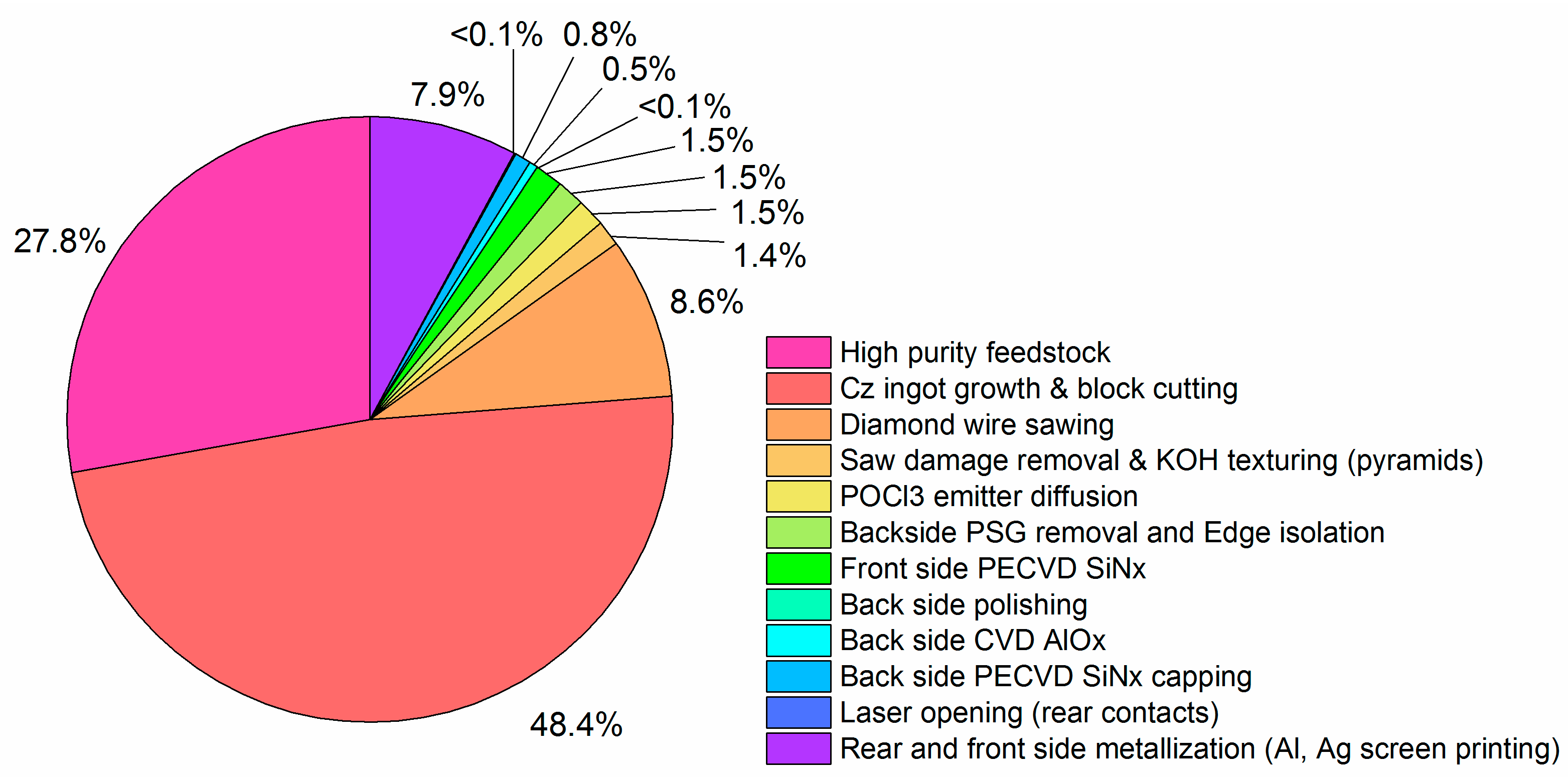
The relative costs for all the processing steps for the texturized Cz-Si and black mc-Si cells are shown in Figure 2 and Figure 3, respectively; where the costs are normalized over the total cost of the respective PERC process. Note that the majority of the costs are related to the costs of the substrates. In addition, the sum of the costs for the cell processing steps that differ between the two device architectures (i.e., corresponding to the process steps highlighted in blue in Figure 1) amounts to ~75% and 65% of the total cell costs for the Cz-Si PERC and the black mc-Si PERC, respectively.
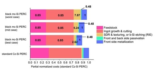
Figure 4 shows the sum of the normalized costs for the PERC process steps that are different between the reference and the black mc-Si PERC. Three cases are calculated for the black mc-Si PERC, corresponding to different costs for the b-Si DRIE step. The reference value (best case) is calculated considering the same step costs as for other b-Si etching methods currently deployed in industry, e.g., atmospheric dry etching (ADE). The remaining two scenarios, i.e., mid and worst scenarios, consider an increase in the etching cost by a factor of 2 and 3, respectively, due to the R&D effort required for the optimization of DRIE tools for industrial PV lines.
The sum of the costs show that the benefit of the adoption of DRIE b-Si is closely related to the potential of using less expensive wafer materials, i.e., mc-Si, whose efficiency and thus cost per unit power is made competitive thanks to the cell power output enhancement provided by the b-Si. The cell processing steps (Steps 4+5, 8–10, and 14) are indeed introducing higher costs per unit power for the black mc-Si PERC compared to the texturized Cz-PERC. However, the b-Si etching by RIE step introduces a cost increase of only a factor of 2.62 in the step cost (best case scenario). Furthermore, the contribution to the total costs due to these steps is limited, and the saving in the cost per unit power allowed by the use mc-Si substrates more than compensates for this, as seen in Figure 4. The cell processing steps that differ between the Cz-Si and black mc-Si PERC architectures amount to 87.5% of the overall costs for the Cz-Si PERC processing, where the contribution of Steps 4+5 and 8–10 accounts for ~2% for each. Therefore, the overall cell processing costs are lower for the black mc-Si PERC even in the worst case scenario as seen in Figure 4 (total costs of the different steps in this scenario are 96.4% of the Cz-Si PERC). In addition, note that the surface passivation steps, albeit providing a limited contribution to the total costs, show yet another potential cost saving, since the black mc-Si PERC can effectively be passivated with a double-side ALD step prior to capping the rear side by SiNx, leading to both lower process costs and a lower number of necessary processing tools. The cost for the surface passivation by double-sided ALD is <50% of the cost for the corresponding steps by PECVD and CVD for the standard Cz process, which also includes an additional back surface polishing step. Therefore, all scenarios calculated in Figure 4 show that there is a cost reduction moving from a standard texturized Cz-Si PERC to a black mc-Si PERC architecture, with up to an 11.7% reduction for the best case scenario, which in turn represents a 10.8% drop in the cost per unit power of the overall PERC cell.
In order to evaluate the capability for the introduction of the DRIE black silicon etching process into manufacturing, the comparison of the costs for the cell processing steps that differ between standard texturized and black-Si PERC cells can be carried out also on similar substrates, i.e., Cz-Si PERC. In this instance, the major differences are related to Steps 1 to 3, which account for 84.9% of the overall cell processing costs. Assuming a 22% efficiency for black Cz-Si PERC cells, the increase in the costs introduced by the combination of black Si etching and consequent passivation by double-side ALD is between 15.8% (best case scenario) and 25.1% (worst case scenario) of the overall cell processing costs. Note that the efficiency premium allowed by the nanostructuring of the silicon surface implies that the cost increases mentioned above are an upper boundary.
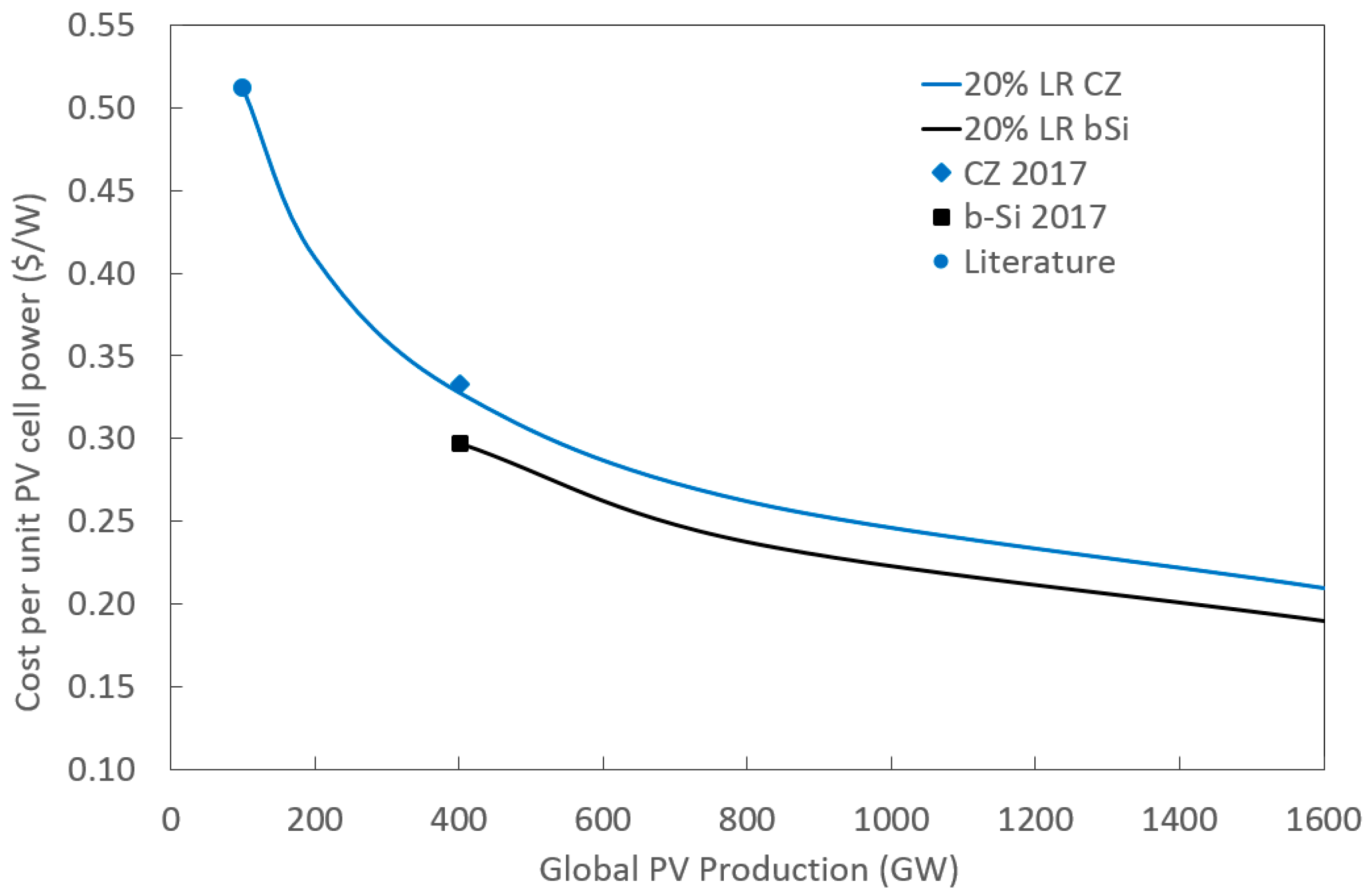
Figure 5 shows the cost per unit of solar photovoltaic cell power ($/W) as a function of global cumulative PV production in GW. The symbols in Figure 5 represent values from the literature extrapolated from [68] and the Cz and black mc-Si values calculated above. The line represents a 20% learning rate taken from the cumulative global PV production values of 100 GW surpassed in 2012 and 401.5 GW, which was obtained in 2017 [69]. The Cz value calculated here (two global PV manufacturing doublings) falls just above the expected 20% learning rate and offers a strong indication that the assumptions made in Section 2 are accurate. As can be seen in Figure 5, with the use of black mc-Si within two more doublings of global PV production the cost per watt of mc-Si cells is expected to drop below 20 cents per Watt. This results in PV-generated LCOE [10] electricity prices below those of all competing technologies by a large enough margin [11] that it can be safely estimated to vastly increase the overall PV market.
A note should be made about the use of absolute cost estimates with the data presented here. The results of a relative 10–12% cost drop for the use of b-Si mc-Si over Cz-Si are valid as long as the cost structures remain relatively constant. These same cost advantages would be present regardless of manipulations of the economics of PV (e.g., government support, companies selling at a loss to maintain market share, trade-war-based tariffs between the U.S. and China, etc.) as long as they were applied equally to both technologies. So, for example, the recent Tamboli, et al. [70] study to estimate the cost of a cadmium telluride and silicon tandem cell inferred that cell costs for Cz-Si from their sources had reached lower $/W values. In their study, Cz-Si materials still dominated the costs. If the percent of the costs are similar to those shown in Figure 1, then additional U.S. cents per watt are potentially saved with b-Si. This would be expected to result in even lower costs for such tandem structures and is left for future work.
4. Discussion
4.1. Black Silicon
The definition of ‘black silicon’ is currently used in the literature and the technical press in reference to etched silicon substrates whose surface achieves vastly diverse degrees of nanostructured features. Both ‘low’ and ‘high’ reflectance un-coated surfaces are called as black silicon, albeit the reflectance in the visible range under AM1.5G illumination conditions differs by one order of magnitude, i.e., well below 2% (by low temperature DRIE [53,57]) and >8% (by plasma immersion ion implantation, PIII [71]), >15% [56] or >30% [72] (by room temperature RIE), respectively. Thus, black silicon is sometimes used as a marketing tool and the Si surfaces referred to as black have various shades in the grey spectrum.
The economic viability of b-Si etched by MACE process has already been proven by its industrial adoption; however, for the first time this work has carefully probed the economic viability for the higher-performance dry-etched b-Si coupled with ALD passivation to replace conventional processing of PERC solar cells. The industrial feasibility of the black mc-Si PERC processing flow considered in this work (Figure 1) has already been verified in a pilot scale PV production line [45]. Thus, the high performance of the DRIE b-Si successfully etched in lab-scale facilities [45] is not expected to hinder in any way a successful upscaling to full industrial PV lines, and its costs are already included in the mid- and worst-case scenarios (Figure 4). Furthermore, the added benefits of b-Si etched by RIE of mitigating the light-induced degradation [28] and of allowing a much wider angle of acceptance [45] in industrial mc-Si PERC cells confirm that the cell efficiencies considered in this work (22%) are feasible within a reasonably short amount of time necessary for industrial process optimization.
This study thus shows that nanostructured silicon is an economically viable solution for advanced solar cell architectures, potentially driving commercial developments towards higher efficiency devices which would make solar energy production globally more cost-effective, and further accelerate the growth of PV’s market share among all energy resources.
Encouraging the development of high-quality b-Si also has benefits for other applications and companies outside of PV. For example, wafer manufactures may have interest in b-Si for e.g., photodetectors [73,74], MEMS [75], or ion mobility spectrometers [76] applications as investments for b-Si for PV on RIE and DRIE etchers would enable them to apply these techniques to other products in the future.
4.2. Policies to Accelerate b-Si Deployment in the PV Industry
4.2.1. Policies for Research Support
First it is clear from the technical literature [26,77,78] that there is still more work to be done to optimize the black mc-Si PERC. For example, studies could look at the optimization of b-Si emitter diffusion [46,79] or contact formation [80] processes or surface morphology to find a balance between reflectance and light trapping [81] and the threshold for the defect levels present after RIE (i.e., the quality of the b-Si in the literature may be above the economic optimum), which could be funded by traditional university research funding programs from national funders such as the National Science Foundation and the Department of Energy in the U.S. and Horizon 2020 [82] in Europe. There is also an opportunity to develop a hybrid process (RIE + ALD) to reduce capex as both are plasma processes and ideally could be realized in one process chamber (or even in an inline tool). Such work could be funded by public private partnerships (P3s) and/or funds specifically targeting small businesses (<500 employees) such as the Small Business Technology Transfer (STTR) and Small Business Innovation Research (SBIR) programs in the U.S. Similarly, the Business Finland investment tool for critical capabilities could be used for funding equipment development such as those focusing on scaling up ALD.
Federal governments can provide R&D spending directly either through national labs or funding universities and companies to do both basic as well as applied R&D. There is considerable academic literature showing the effectiveness and need of research and development policies at the federal level [83,84,85,86,87,88,89]. Mamuneas et al. [90] have shown that publicly financed R&D created cost savings for industry, but also reduced privately-financed R&D investment, while using secondary sources of policy support such as incremental R&D tax credits and deductibility provision of R&D expenditures increase privately financed R&D investment [90]. More recent studies have shown that federal R&D funding stimulates additional private R&D investments [91]. This area of policy is still under active debate, but it is clear that governments should seek to find an optimal mix of both types of policy instruments to sustain balanced growth in productivity and output in the manufacturing sector [90].
4.2.2. Policies for Commercialization Support
However, even without additional theoretical, technical, or optimization-based research, this study has made clear that existing technology of the black mc-Si PERC will drive down cost for PV. Companies wishing to move to this more advanced PV structure, however, need to invest in RIE and ALD systems scaled to the sizes necessary in the PV industry. Currently, RIE tools of this scale are available for room temperature RIE [92] and spatial ALD tools are already being sold (e.g., AlOx deposition in PERC cells [93], transparent conductive oxides (TCO) [94], organic light emitting diodes (OLEDs) [95,96], or porous Li-ion batteries [97]). The global production of such tools could quickly meet the GW requirements of a modern PV plant given effective policy support.
A particular risk in such policy areas is if the public–private dynamics are not well aligned to encourage solid research of proof-of-concept (such as with b-Si discussed here) and the required infratechnologies (infrastructure technologies such as in this case, PV industry-scaled RIE, and ALD tools), then these promising advances in applied science can easily fall into the so-called “valley of death” and fail to enter the marketplace because the ideas cannot mature into modern advanced manufacturing technologies [98].
The largest challenge to escape the valley of death is the capital costs associated with PV industry-scaled RIE and ALD tools, which are both on the order of several million USD for a 1 GW PV plant. There are several methods that a government can utilize to effectively assist industry in this respect by providing business incentive policies including: R&D tax credits and writedowns by performing large scale research with novel production equipment [99,100,101], loans [102], guarantees/government managed risk [103], subsidies, and most radically purchase/donations (100% subsidies) [104]. In addition, these policies can be spread for example by including the R&D tax credits through multinational tax rules. Even in the most extreme examples of direct subsidies to bolster manufacturing [104,105] there is evidence that both federal and regional (provisional or state) governments earn a positive return on investment (ROI) from revenues for the governments from taxation (personal, corporate, and on sales), sales of products locally (e.g., PV modules), and the saved health, environmental, and economic costs associated with offsetting coal-fired electricity with the use of solar power [105]. Bartik also has provided empirical data that even local and regional government support of industry increases job growth, which results in long-term lower unemployment, higher real estate values, higher labor force participation, and better occupational opportunities for those living in the region [106].
The results of this study indicate there are several interesting opportunities for governments to enjoy a large ROI for providing an incentive for companies to scale-up RIE and ALD specifically for the conversion of mc-Si PV manufacturing plants to begin b-Si PV manufacturing. The results of studies on the benefits of government support of PV manufacturing (which have focused on the entire plant) [105,107] would be enhanced here as the necessary infrastructure investments are for a small portion of the plant (e.g., only RIE and ALD systems). With successful deployment of b-Si manufacturing, PV from the plant would have approximately 10% lower costs for an equivalent aggregate power of PV deployed. With all variables being held constant, this would be expected to increase the market and increase the demand for larger production volumes, which would in turn increase the income side for the government (e.g., larger taxes and increased environmental and health benefits) and improve the ROI.
Although many governments are interested in boosting domestic renewable energy manufacturing, China has already made the expansion of renewable energy one of the business areas which receive special attention under China’s five-year plans, including loans and tax incentives [108]. China already dominates global PV manufacturing [109,110] and thus has the most mc-Si plants, which provide a geographic advantage for applying relatively small policy support needed to accelerate b-Si PV manufacturing and recoup the benefits. China is not the only country that could see an advantage. In the countries of the European Union with a significantly weakened presence in PV manufacturing itself, but a strong presence in PV manufacturing equipment, the development of large-scale RIE and ALD devices to meet the needs of the global PV manufacturing market represents a significant opportunity. For example, Finland, a world-leader in ALD tool manufacturing, could strategically invest in industrial focused R&D to make a large-scale ALD system specifically for b-Si passivation for the rapidly growing PV industry. Finnish companies in these areas would benefit from programs like the normal project support from Business Finland (BF) or through Ecsel JU jointly with BF. How this strategic investment is done is country dependent. For example, in the U.S., several studies have shown a considerable benefit to from the Research and Experimentation Credit [111,112,113]. While, in Finland, the results of tax breaks have been more mixed [114,115] and direct support for R&D costs is more effective, particularly for small and medium sized enterprises (SMEs) and startups.
5. Conclusions
This study has presented the costs involved in the replacement of standard Cz-Si PERC cells with black-Si PERC cells. The increase in the overall cell processing costs due to the addition of the steps for the etching of the black Si surface is overcome by multiple benefits generated by the nanostructuring process (e.g., improved performance, hindered power conversion efficiency degradation, and enhanced metal gettering) and by the possibility to use effective double-side ALD passivation. Thus, the adoption of black Si PERC cells becomes highly attractive for the PV industry. When combining mc-Si substrates with the deployment of black Si PERC technology, the PV industry will be able to reduce the partial processing costs by approximately 11.7% by replacing the standard Cz-Si PERC. This represents a 10.8% drop in the cost per unit power of the overall PERC cell fabrication process, which could have a profound effect on the deployment rate of across all PV applications. These are significant cost savings and thus energy policies are reviewed to overcome challenges to accelerating the deployment of black mc-Si PERC across the PV industry. The energy policy recommendations that would be most useful for helping industry are primarily focused around reducing the risk associated investing in the multimillion dollar capital costs of RIE and ALD equipment needed to produce at the GW scale. There are nationally strategic policies that would provide R&D to scale these tools as well as policies to ease and scale the commercial deployment of these tools in order to enjoy the return from an increased PV market at lower costs.
Author Contributions
Conceptualization, C.M., H.S. and J.P.; Data curation, C.M. and J.P.; Formal analysis, C.M., H.S.L., T.P.P., H.S. and J.P.; Funding acquisition, T.P.P., H.S. and J.P.; Investigation, C.M.; Methodology, C.M.; Project administration, H.S.; Resources, H.S.; Supervision, H.S.; Writing–original draft, C.M. and J.P.; Writing–review & editing, C.M., H.S.L., T.P.P., H.S. and J.P.
Funding
This work was partially funded by Fulbright Finland and the BLACK-project (project no. 2956/31/2014) which was supported under the umbrella of SOLAR-ERA.NET by Business Finland (former Tekes–the Finnish Funding Agency for Innovation). T.P. Pasanen acknowledges the Aalto ELEC Doctoral School, Jenny and Antti Wihuri Foundation, and Walter Ahlström Foundation for the financial support.
Acknowledgments
The authors would like to thank the industrial and research partners of the BLACK project for helpful discussions.
Conflicts of Interest
The authors declare no conflict of interest. The founding sponsors had no role in the design of the study; in the collection, analyses, or interpretation of data; in the writing of the manuscript, or in the decision to publish the results.
Nomenclature
| ADE | Atmospheric dry etching |
| Ag | Silver |
| Al | Aluminum |
| ALD | Atomic layer deposition |
| AlOx | Aluminum oxide |
| b-Si | Black silicon |
| CVD | Chemical vapor deposition |
| Cz | Czochralski |
| DRIE | Deep reactive ion etching |
| KOH | Potassium hydroxide |
| LID | Light induced degradation |
| MACE | Metal-assisted chemical etching |
| mc-Si | Multicrystalline silicon |
| PECVD | Plasma enhanced chemical vapor deposition |
| PERC | Passivated emitter rear cell |
| POCl3 | Phosphoryl chloride |
| PSG | Phosphosilicate glass |
| PV | Photovoltaic |
| RIE | Reactive ion etching |
| R&D | Research and development |
| ROI | Return on investment |
| SDR | Saw damage removal |
| SiNx | Silicon nitride |
| SME | Small and medium sized enterprises |
| TCO | Transparent conductive oxide |
Appendix A. Costs of All the Production Steps for Both the Standard (Texturized) Cz PERC and the Black Multicrystalline PERC.

| Process Step | Step Costs (US$/Wp) Standard (Texturized) Cz PERC | Source | Step Costs (US$/Wp) Black mc-Si PERC | Source |
|---|---|---|---|---|
| 1 * | 0.0925 | [68] | 0.0786 | [68] |
| 2 * | 0.1610 | [68] | 0.1369 | [68] |
| 3 * | 0.0287 | [68] | 0.0287 | [68] |
| 4+5 | 0.0045 | § | 0.0118 (best case) | § |
| 0.0236 (mid case) | ||||
| 0.0354 (worst case) | ||||
| 6 | 0.0050 | § | 0.0050 | § |
| 7 | 0.0049 | § | 0.0049 | § |
| 8 | 0.0049 | § | 0.0031 | § |
| 9 | 0.0000 | § | ||
| 10 | 0.0016 | § | ||
| 11 | 0.0028 | § | 0.0011 | § |
| 12 | 0.0003 | § | 0.0003 | § |
| 13+14 | 0.0263 | § | 0.0263 | § |
* Note that the difference in the costs of Steps 1 to 3 is calculated considering the difference in the spot prices in high purity Cz silicon and high-performance mc-Si retrieved in February 2018. § Proprietary industry information provided under conditions of anonymity.
Appendix B
| Source | PERC Cell Architecture | Assumptions | ||
|---|---|---|---|---|
| Cell Size * | Cell Efficiency | Cell Output | ||
| [68] | Both | cm2 | % | Wp/cell |
| 237 | 22 | 5.204 | ||
| § | Standard (texturized) Cz PERC | 244 | 22 | 5.375 |
| Black mc-Si PERC | 246 | 22 | 5.405 | |
| § | Black mc-Si PERC | 243 | 22 | 5.204 |
| § | Black mc-Si PERC | 243 | 22 | 5.204 |
* Cell parameters considered in the calculations of the process steps costs. Small variations in the cell size depend on the industrial standard substrate available at the data source at the moment of data retrieval. § Proprietary industry information provided under conditions of anonymity.
References
- Albrecht, J. The future role of photovoltaics: A learning curve versus portfolio perspective. Energy Policy 2007, 35, 2296–2304. [Google Scholar] [CrossRef]
- Yu, C.F.; van Sark, W.G.J.H.M.; Alsema, E.A. Unraveling the photovoltaic technology learning curve by incorporation of input price changes and scale effects. Renew. Sustain. Energy Rev. 2011, 15, 324–337. [Google Scholar] [CrossRef]
- Hong, S.; Chung, Y.; Woo, C. Scenario analysis for estimating the learning rate of photovoltaic power generation based on learning curve theory in South Korea. Energy 2015, 79, 80–89. [Google Scholar] [CrossRef]
- Trappey, A.J.C.; Trappey, C.V.; Tan, H.; Liu, P.H.Y.; Li, S.-J.; Lin, L.-C. The determinants of photovoltaic system costs: an evaluation using a hierarchical learning curve model. J. Clean. Prod. 2016, 112, 1709–1716. [Google Scholar] [CrossRef]
- Mauleón, I. Photovoltaic learning rate estimation: Issues and implications. Renew. Sustain. Energy Rev. 2016, 65, 507–524. [Google Scholar] [CrossRef]
- Feldman, D.; Barbose, G.; Margolis, R.; Wiser, R.; Darghout, N.; Goodrich, A. Photovoltaic (PV) Pricing Trends: Historical, Recent, and Near-term Projections; Technical Report; Lawrence Berkeley National Lab.: Berkeley, CA, USA, 2012. [Google Scholar]
- Barbose, G.L.; Darghouth, N.R.; Millstein, D.; LaCommare, K.; DiSanti, N.; Widiss, R. Tracking the Sun 10: The Installed Price of Residential and Non-Residential Photovoltaic Systems in the United States. Available online: https://emp.lbl.gov/publications/tracking-sun-10-installed-price (accessed on 25 July 2018).
- PVinsights. Available online: http://pvinsights.com/ (accessed on 25 July 2018).
- Reuters. Solar Costs to Fall Further, Powering Global Demand-Irena. Available online: https://www.reuters.com/article/singapore-energy-solar/solar-costs-to-fall-further-powering-global-demand-irena-idUSL4N1MY2F8 (accessed on 5 March 2018).
- Branker, K.; Pathak, M.J.M.; Pearce, J.M. A review of solar photovoltaic levelized cost of electricity. Renew. Sustain. Energy Rev. 2011, 15, 4470–4482. [Google Scholar] [CrossRef]
- Safi, M. Indian Solar Power Prices Hit Record Low, Undercutting Fossil Fuels. Available online: http://www.theguardian.com/environment/2017/may/10/indian-solar-power-prices-hit-record-low-undercutting-fossil-fuels (accessed on 5 March 2018).
- Drury, E.; Miller, M.; Macal, C.M.; Graziano, D.J.; Heimiller, D.; Ozik, J.; Perry, T.D., IV. The transformation of southern California’s residential photovoltaics market through third-party ownership. Energy Policy 2012, 42, 681–690. [Google Scholar] [CrossRef]
- Branker, K.; Shackles, E.; Pearce, J.M. Peer-to-peer financing mechanisms to accelerate renewable energy deployment. J. Sustain. Financ. Invest. 2011, 1, 138–155. [Google Scholar] [CrossRef]
- Alafita, T.; Pearce, J.M. Securitization of residential solar photovoltaic assets: Costs, risks and uncertainty. Energy Policy 2014, 67, 488–498. [Google Scholar] [CrossRef]
- Hede, S.; Nunes, M.J.L.; Ferreira, P. Credits trading mechanism for corporate social responsibility: An empirically grounded framework. Int. J. Technol. Learn. Innov. Dev. 2014, 7, 49–92. [Google Scholar] [CrossRef]
- Overholm, H. Spreading the rooftop revolution: What policies enable solar-as-a-service? Energy Policy 2015, 84, 69–79. [Google Scholar] [CrossRef]
- Ameli, N.; Kammen, D.M. Innovations in financing that drive cost parity for long-term electricity sustainability: An assessment of Italy, Europe’s fastest growing solar photovoltaic market. Energy Sustain. Dev. 2014, 19, 130–137. [Google Scholar] [CrossRef]
- Coughlin, J.; Cory, K.S. Solar Photovoltaic Financing: Residential Sector Deployment; Technical Report; National Renewable Energy Laboratory: Golden, CO, USA, 2009. [Google Scholar]
- International Energy Agency. Renewables 2017. Available online: https://www.iea.org/publications/renewables2017/ (accessed on 5 March 2018).
- Polman, A.; Knight, M.; Garnett, E.C.; Ehrler, B.; Sinke, W.C. Photovoltaic materials: Present efficiencies and future challenges. Science 2016, 352, aad4424. [Google Scholar] [CrossRef] [PubMed]
- Projected Market Share of Solar Photovoltaic Panels Worldwide in 2030, by Technology. Available online: https://www.statista.com/statistics/492755/solar-pv-panels-market-share-projection-by-cell-technology-globally/ (accessed on 5 March 2018).
- Powell, D.M.; Fu, R.; Horowitz, K.; Basore, P.A.; Woodhouse, M.; Buonassisi, T. The capital intensity of photovoltaics manufacturing: Barrier to scale and opportunity for innovation. Energy Environ. Sci. 2015, 8, 3395–3408. [Google Scholar] [CrossRef]
- Dullweber, T.; Schmidt, J. Industrial silicon solar cells applying the passivated emitter and rear cell (PERC) concept—A review. IEEE J. Photovolt. 2016, 6, 1366–1381. [Google Scholar] [CrossRef]
- Green, M.A. The Passivated Emitter and Rear Cell (PERC): From conception to mass production. Sol. Energy Mater. Sol. Cells 2015, 143, 190–197. [Google Scholar] [CrossRef]
- International Technology Roadmap for Photovoltaic Results 2016 incl. Maturity Report. Available online: http://www.itrpv.net/Reports/Downloads/ (accessed on 16 May 2018).
- Liu, X.; Coxon, P.R.; Peters, M.; Hoex, B.; Cole, J.M.; Fray, D.J. Black silicon: Fabrication methods, properties and solar energy applications. Energy Environ. Sci. 2014, 7, 3223–3263. [Google Scholar] [CrossRef]
- Pasanen, T.P.; Laine, H.S.; Vähänissi, V.; Schön, J.; Savin, H. Black silicon significantly enhances phosphorus diffusion gettering. Sci. Rep. 2018, 8, 1991. [Google Scholar] [CrossRef] [PubMed]
- Pasanen, T.P.; Modanese, C.; Vähänissi, V.; Laine, H.S.; Heikkinen, I.T.S.; Wolny, F.; Oehlke, A.; Kusterer, K.; Wagner, Mt.; Savin, H. Black-silicon eliminates light- and elevated-temperature induced degradation in industrial passivated emitter and rear cells. Prog. Photovolt. 2018. under review. [Google Scholar]
- Davidsen, R.S.; Ormstrup, J.; Ommen, M.L.; Larsen, P.E.; Schmidt, M.S.; Boisen, A.; Nordseth, Ø.; Hansen, O. Angle resolved characterization of nanostructured and conventionally textured silicon solar cells. Sol. Energy Mater. Sol. Cells 2015, 140, 134–140. [Google Scholar] [CrossRef] [Green Version]
- Koynov, S.; Brandt, M.S.; Stutzmann, M. Black nonreflecting silicon surfaces for solar cells. Appl. Phys. Lett. 2006, 88. [Google Scholar] [CrossRef]
- Jura, M.P.; Miller, J.B.; Yim, J.W.L.; Forziati, J.; Murphy, B.; Chleboski, R.; Cooper, I.B.; Rohatgi, A.; Black, M.R. Conventionally-processed silicon nanowire solar cells demonstrating efficiency improvement over standard cells. In Proceedings of the 2014 IEEE 40th Photovoltaic Specialist Conference (PVSC), Denver, CO, USA, 8–13 June 2014; pp. 598–600. [Google Scholar]
- Toor, F.; Miller, J.B.; Davidson, L.M.; Nichols, L.; Duan, W.; Jura, M.P.; Yim, J.; Forziati, J.; Black, M.R. Nanostructured silicon via metal assisted catalyzed etch (MACE): chemistry fundamentals and pattern engineering. Nanotechnology 2016, 27, 412003. [Google Scholar] [CrossRef] [PubMed]
- Toor, F.; Miller, J.B.; Davidson, L.M.; Duan, W.; Jura, M.P.; Yim, J.; Forziati, J.; Black, M.R. Metal assisted catalyzed etched (MACE) black Si: optics and device physics. Nanoscale 2016, 8, 15448–15466. [Google Scholar] [CrossRef] [PubMed]
- Beetz, B. Suntech’s Black Silicon Solar Cells Enter Mass Production. Available online: https://www.pv-magazine.com/2018/01/04/suntechs-black-silicon-solar-cells-enter-mass-production/ (accessed on 8 March 2018).
- Hutchins, M. Black is the New Black. Available online: https://www.pv-magazine.com/magazine-archive/black-is-the-new-black/ (accessed on 5 March 2018).
- Savin, H.; Repo, P.; Gastrow, G.V.; Ortega, P.; Calle, E.; Garín, M.; Alcubilla, R. Black silicon solar cells with interdigitated back-contacts achieve 22.1% efficiency. Nat. Nanotechnol. 2015, 10, 624–628. [Google Scholar] [CrossRef] [PubMed] [Green Version]
- Davidsen, R.S.; Li, H.; To, A.; Wang, X.; Han, A.; An, J.; Colwell, J.; Chan, C.; Wenham, A.; Schmidt, M.; et al. Black silicon laser-doped selective emitter solar cell with 18.1% efficiency. Sol. Energy Mater. Sol. Cells 2016, 144, 740–747. [Google Scholar] [CrossRef] [Green Version]
- Werner, S.; Lohmüller, E.; Saint-Cast, P.; Greulich, J.M.; Weber, J.; Schmidt, S.; Moldovan, A.; Brand, A.A.; Dannenber, T.; Mack, S.; et al. Key aspects for fabrication of p-type Cz-Si PERC solar cells exceeding 22% conversion efficiency. In Proceedings of the the 33rd European PV Solar Energy Conference and Exhibition, Amsterdam, The Netherlands, 25–29 September 2017. [Google Scholar]
- NREL. Solar Spectra. Air Mass 1.5: ASTM G-173-03. Available online: http://rredc.nrel.gov/solar/spectra/am1.5/ (accessed on 5 March 2018).
- Energy Trend PV. Available online: https://pv.energytrend.com/ (accessed on 2 June 2018).
- Priolo, F.; Gregorkiewicz, T.; Galli, M.; Krauss, T.F. Silicon nanostructures for photonics and photovoltaics. Nat. Nanotechnol. 2014, 9, 19–32. [Google Scholar] [CrossRef] [PubMed]
- Venkatesan, R.; Arivalagan, M.K.; Venkatachalapathy, V.; Pearce, J.M.; Mayandi, J. Effects of silver catalyst concentration in metal assisted chemical etching of silicon. Mater. Lett. 2018, 221, 206–210. [Google Scholar] [CrossRef]
- Saint-Cast, P.; Kafle, B.; Pandey, R.; Ridoy, A.I.; Hofmann, M.; Clochard, L.; Schwarze, T.; Pittroff, M.; Rentsch, J.; Preu, R. Rear passivated mc-Si solar cells textured by atmospheric pressure dry etching. Energy Procedia 2017, 124, 260–266. [Google Scholar] [CrossRef]
- Repo, P.; Haarahiltunen, A.; Sainiemi, L.; Yli-Koski, M.; Talvitie, H.; Schubert, M.C.; Savin, H. Effective Passivation of Black Silicon Surfaces by Atomic Layer Deposition. IEEE J. Photovolt. 2013, 3, 90–94. [Google Scholar] [CrossRef] [Green Version]
- Pasanen, T.P.; Vähänissi, V.; Wolny, F.; Oehlke, A.; Wagner, M.; Juntunen, M.A.; Heikkinen, I.T.S.; Salmi, E.; Sneck, S.; Vahlman, H.; et al. Industrial applicability of AR-coating-free black silicon. In Proceedings of the 35th European PV Solar Energy Conference and Exhibition (EU PVSEC), Brussels, Belgium, 24–28 September 2018. [Google Scholar]
- Heikkinen, I.T.S.; Repo, P.; Vähänissi, V.; Pasanen, T.; Malinen, V.; Savin, H. Efficient surface passivation of black silicon using spatial atomic layer deposition. Energy Procedia 2017, 124, 282–287. [Google Scholar] [CrossRef]
- Dingemans, G.; Terlinden, N.M.; Verheijen, M.A.; van de Sanden, M.C.M.; Kessels, W.M.M. Controlling the fixed charge and passivation properties of Si(100)/Al2O3 interfaces using ultrathin SiO2 interlayers synthesized by atomic layer deposition. J. Appl. Phys. 2011, 110, 093715. [Google Scholar] [CrossRef]
- Terlinden, N.M.; Dingemans, G.; Vandalon, V.; Bosch, R.H.E.C.; Kessels, W.M.M. Influence of the SiO2 interlayer thickness on the density and polarity of charges in Si/SiO2/Al2O3 stacks as studied by optical second-harmonic generation. J. Appl. Phys. 2014, 115, 033708. [Google Scholar] [CrossRef]
- Pasanen, T.P.; Vähänissi, V.; Theut, N.; Savin, H. Surface passivation of black silicon phosphorus emitters with atomic layer deposited SiO2/Al2O3 Stacks. Energy Procedia 2017, 124, 307–312. [Google Scholar] [CrossRef]
- Loo, B.H.W.V.D.; Knoops, H.C.M.; Dingemans, G.J.M.; Lamers, M.W.P.E.; Romijn, I.G.; Weeber, A.W.; Kessels, W.M.M. ”Zero-charge” SiO2/Al2O3 stacks for the simultaneous passivation of n+ and p+ doped silicon surfaces by atomic layer deposition. Sol. Energy Mater. Sol. Cells 2015, 143, 450–456. [Google Scholar]
- Cui, J.; Wan, Y.; Chen, Y.; Verlinden, P.; Cuevas, A. Highly effective electronic passivation of silicon surfaces by atomic layer deposited hafnium oxide. Appl. Phys. Lett. 2017, 110, 021602. [Google Scholar] [CrossRef]
- Ingenito, A.; Isabella, O.; Zeman, M. Nano-cones on micro-pyramids: modulated surface textures for maximal spectral response and high efficiency solar cells. Prog. Photovolt. Res. Appl. 2015, 23, 1649–1659. [Google Scholar] [CrossRef]
- Gastrow, G.V.; Alcubilla, R.; Ortega, P.; Yli-Koski, M.; Conesa-Boj, S.; Fontcuberta I Morral, A.; Savin, H. Analysis of the atomic layer deposited Al2O3 field-effect passivation in black silicon. Sol. Energy Mater. Sol. Cells 2015, 142, 29–33. [Google Scholar] [CrossRef] [Green Version]
- To, A.; Li, W.M.; Li, X.; Hoex, B. The effects of bifacial deposition of ALD AlOx on the contact properties of screen-printed contacts for p-type PERC solar cells. Energy Procedia 2017, 124, 914–921. [Google Scholar] [CrossRef]
- Müller, M.; Fischer, G.; Bitnar, B.; Steckemetz, S.; Schiepe, R.; Mühlbauer, M.; Köhler, R.; Richter, P.; Kusterer, C.; Oehlke, A.; et al. Loss analysis of 22% efficient industrial PERC solar cells. Energy Procedia 2017, 124, 131–137. [Google Scholar] [CrossRef]
- Wang, W.; Donw, J.; Ye, Q.; Yang, Y.; Cai, W.; Sheng, J.; Yang, J.; Zhang, C.; Zhou, X.; Dong, S. Industrially feasible PERC cells on diamond wire sawing multi-crystalline silicon wafers textured by RIE towards 20.78% efficiency. In Proceedings of the 33rd European Photovoltaic Solar Energy Conference and Exhibition, Amsterdam, The Netherlands, 25–29 September 2017; pp. 290–294. [Google Scholar]
- Repo, P.; Benick, J.; Gastrow, G.V.; Vähänissi, V.; Heinz, F.D.; Schön, J.; Schubert, M.C.; Savin, H. Passivation of black silicon boron emitters with atomic layer deposited aluminum oxide. Phys. Status Solidi RRL 2013, 7, 950–954. [Google Scholar] [CrossRef] [Green Version]
- Otto, M.; Kroll, M.; Käsebier, T.; Salzer, R.; Tünnermann, A.; Wehrspohn, R.B. Extremely low surface recombination velocities in black silicon passivated by atomic layer deposition. Appl. Phys. Lett. 2012, 100, 191603. [Google Scholar] [CrossRef]
- Pvbuzz Media. Get Read-The Price for Solar Power Will Drop Even Further. Available online: https://www.pvbuzz.com/price-for-solar-power-drop/ (accessed on 25 February 2018).
- Strupeit, L.; Neij, L. Cost dynamics in the deployment of photovoltaics: Insights from the German market for building-sited systems. Renew. Sustain. Energy Rev. 2017, 69, 948–960. [Google Scholar] [CrossRef]
- Nemet, G.F. Beyond the learning curve: factors influencing cost reductions in photovoltaics. Energy Policy 2006, 34, 3218–3232. [Google Scholar] [CrossRef]
- Parente, V.; Goldemberg, J.; Zilles, R. Comments on experience curves for PV modules. Prog. Photovolt. Res. Appl. 2002, 10, 571–574. [Google Scholar] [CrossRef]
- Candelise, C.; Winskel, M.; Gross, R.J.K. The dynamics of solar PV costs and prices as a challenge for technology forecasting. Renew. Sustain. Energy Rev. 2013, 26, 96–107. [Google Scholar] [CrossRef] [Green Version]
- Breyer, C.; Birkner, C.; Kersten, F.; Gerlach, A.; Goldschmidt, J.C.; Stryi-Hipp, G.; Fraile Montoro, D.; Riede, M. Research and Development Investments in PV–A Limiting Factor for a Fast PV Diffusion? In Proceedings of the 25th European Photovoltaic Solar Energy Conference and Exhibition, Valencia, Spain, 6–10 September 2010. [Google Scholar]
- Tour, A.D.L.; Glachant, M.; Ménière, Y. Predicting the costs of photovoltaic solar modules in 2020 using experience curve models. Energy 2013, 62, 341–348. [Google Scholar] [CrossRef]
- Swanson, R.M. A vision for crystalline silicon photovoltaics. Prog. Photovolt. Res. Appl. 2006, 14, 443–453. [Google Scholar] [CrossRef] [Green Version]
- Ferioli, F.; van der Zwaan, B.C.C. Learning in Times of Change: A Dynamic Explanation for Technological Progress. Environ. Sci. Technol. 2009, 43, 4002–4008. [Google Scholar] [CrossRef] [PubMed] [Green Version]
- Goodrich, A.; Hacke, P.; Wang, Q.; Sopori, B.; Margolis, R.; James, T.L.; Woodhouse, M. A wafer-based monocrystalline silicon photovoltaics road map: Utilizing known technology improvement opportunities for further reductions in manufacturing costs. Sol. Energy Mate. Sol. Cells 2013, 114, 110–135. [Google Scholar] [CrossRef]
- Hill, J.S. Global Solar Market Demand Expected to Reach 100 Gigawatts in 2017, Says Solar Power Europe. Available online: https://cleantechnica.com/2017/10/27/global-solar-market-demand-expected-reach-100-gw-2017-solarpower-europe/ (accessed on 23 May 2018).
- Tamboli, A.C.; Bobela, D.C.; Kanevce, A.; Remo, T.; Alberi, K.; Woodhouse, M. Low-Cost CdTe/Silicon Tandem Solar Cells. IEEE J. Photovolt. 2017, 7, 1767–1772. [Google Scholar] [CrossRef]
- Liu, J.; Liu, B.; Shen, Z.; Liu, J.; Zhong, S.; Liu, S.; Li, C.; Xia, Y. Characterization of PIII textured industrial multicrystalline silicon solar cells. Sol. Energy 2012, 86, 3004–3008. [Google Scholar] [CrossRef]
- Yoo, J.; Yu, G.; Yi, J. Large-area multicrystalline silicon solar cell fabrication using reactive ion etching (RIE). Sol. Energy Mater. Sol. Cells 2011, 95, 2–6. [Google Scholar] [CrossRef]
- Juntunen, M.; Heinonen, J.; Vähänissi, V.; Repo, P.; Valluru, D.; Savin, H. Near-unity quantum efficiency of broadband black silicon photodiodes with an induced junction. Nat. Photonics 2016, 10, 777–781. [Google Scholar] [CrossRef]
- Huang, Z.; Carev, J.E.; Liu, M.; Mazur, E.; Campbell, J.C. Microstructured silicon photodetector. Appl. Phys. Lett. 2006, 89, 033506. [Google Scholar] [CrossRef]
- Boer, M.J.; Gardeniers, J.G.E.; Jansen, H.V.; Gilde, M.J.; Roelofs, G.; Sasserath, J.N.; Elwenspoek, M.C. Guidelines for etching silicon MEMS structures using fluorine high-density plasmas at cryogenic temperatures. J. Microelectromech. Syst. 2002, 11, 385–401. [Google Scholar] [CrossRef] [Green Version]
- Gesemann, B.; Wehrspohn, R.; Hackner, A.; Müller, G. Large-Scale Fabrication of Ordered Silicon Nanotip Arrays Used for Gas Ionization in Ion Mobility Spectrometers. IEEE Trans. Nanotechnol. 2011, 10, 50–52. [Google Scholar] [CrossRef]
- Joshi, M.; Verma, R. Black Silicon Photovoltaics: Fabrication methods and properties. Int. J. Res. Eng. Sci. 2017, 5, 62–72. [Google Scholar]
- Lv, J.; Zhang, T.; Zhang, P.; Zhao, Y.; Li, S. Review application of nanostructured black silicon. Nanoscale Res. Lett. 2018, 13, 110. [Google Scholar] [CrossRef] [PubMed]
- Kafle, B.; Schön, J.; Fleischmann, C.; Werner, S.; Wolf, A.; Clochard, L.; Duffy, E.; Hofmann, M.; Rentsch, J. On the emitter formation in nanotextured silicon solar cells to achieve improved electrical performances. Sol. Energy Mater. Sol. Cells 2016, 152, 94–102. [Google Scholar] [CrossRef]
- Repo, P.; Benick, J.; Vähänissi, V.; Schön, J.; von Gastrow, G.; Steinhauser, B.; Schubert, M.C.; Hermle, M.; Savin, H. N-type Black Silicon Solar Cells. Energy Procedia 2013, 38, 866–871. [Google Scholar] [CrossRef]
- Peyronnet, R.; Fischer, G.; Blevin, T.; Johnson, E.V.; Drahi, E.; Lemiti, M. Texturing optimization for bifacial n-PERT: Are pyramids and/or black silicon the way to go for thinner devices? Energy Procedia 2017, 124, 250–259. [Google Scholar] [CrossRef]
- What is Horizon 2020? Available online: https://ec.europa.eu/programmes/horizon2020/en/what-horizon-2020 (accessed on 25 April 2018).
- Griliches, Z. Research Costs and Social Returns: Hybrid Corn and Related Innovations. J. Political Econ. 1958, 66, 419–431. [Google Scholar] [CrossRef]
- Griliches, Z. The Search for R&D Spillovers. Available online: http://www.nber.org/papers/w3768 (accessed on 25 July 2018).
- Lenoir, T. Revolution from above: The role of the state in creating the german research system, 1810–1910. Am. Econ. Rev. 1998, 88, 22–27. [Google Scholar]
- Jones, C.I.; Williams, J.C. Measuring the Social Return to R&D. Q. J. Econ. 1998, 113, 1119–1135. [Google Scholar] [CrossRef] [Green Version]
- Hall, B.H. The Financing of Research and Development. Oxf. Rev. Econ. Policy 2002, 18, 35–51. [Google Scholar] [CrossRef] [Green Version]
- Hall, B.H.; Lerner, J. Chapter 14-The Financing of R&D and Innovation. Handb. Econ. Innov. 2010, 1, 609–639. [Google Scholar]
- Levin, R.C.; Klevorick, A.K.; Nelson, R.R.; Winter, S.G.; Gilbert, R.; Griliches, Z. Appropriating the Returns from Industrial Research and Development. Brook. Pap. Econ. Act. 1987, 3, 783–831. [Google Scholar] [CrossRef]
- Mamuneas, T.P.; Ishaq Nadiri, M. Public R&D policies and cost behavior of the US manufacturing industries. J. Public Econ. 1996, 63, 57–81. [Google Scholar] [CrossRef]
- Becker, B. Public R&D Policies and Private R&d Investment: A Survey of the Empirical Evidence. J. Econ. Surv. 2015, 29, 917–942. [Google Scholar] [CrossRef]
- SENTECH: Home of Thin Film Measurement. Available online: https://www.sentech.com/en/site__2235/ (accessed on 29 May 2018).
- InPassion ALD. Available online: http://www.solaytec.com/products/inpassion-ald (accessed on 29 May 2018).
- Lotus Applied Technology. Applications. Available online: http://lotusat.com/roll-to-roll-ald/applications/ (accessed on 29 May 2018).
- Tseng, M.-H.; Yu, H.-H.; Chou, K.-Y.; Jou, J.-H.; Lin, K.-L.; Wang, C.-C.; Tsai, F.-Y. Low-temperature gas-barrier films by atomic layer deposition for encapsulating organic light-emitting diodes. Nanotechnology 2016, 27, 295706. [Google Scholar] [CrossRef] [PubMed]
- Maydannik, P.S.; Kääriäinen, T.O.; Lahtinen, K.; Cameron, D.C.; Söderlund, M.; Soininen, P.; Johansson, P.; Kuusipalo, J.; Moro, L.; Zeng, X. Roll-to-roll atomic layer deposition process for flexible electronics encapsulation applications. J. Vac. Sci. Technol. A 2014, 32, 051603. [Google Scholar] [CrossRef]
- Yersak, A.S.; Sharma, K.; Wallas, J.M.; Dameron, A.A.; Li, X.; Yang, Y.; Hurst, K.E.; Ban, C.; Tenent, R.C.; George, S.M. TEMAZ/O3 atomic layer deposition process with doubled growth rate and optimized interface properties in metal–insulator–metal capacitors. J. Vac. Sci. Technol. A 2018, 36, 01A123. [Google Scholar] [CrossRef]
- Tassey, G. Competing in Advanced Manufacturing: The Need for Improved Growth Models and Policies. J. Econ. Perspect. 2014, 28, 27–48. [Google Scholar] [CrossRef]
- Bloom, N.; Griffith, R.; Van Reenen, J. Do R&D tax credits work? Evidence from a panel of countries 1979–1997. J. Public Econ. 2002, 85, 1–31. [Google Scholar] [CrossRef]
- Rao, N. Do tax credits stimulate R&D spending? The effect of the R&D tax credit in its first decade. J. Public Econ. 2016, 140, 1–12. [Google Scholar] [CrossRef]
- Czarnitzki, D.; Hanel, P.; Rosa, J.M. Evaluating the impact of R&D tax credits on innovation: A microeconometric study on Canadian firms. Res. Policy 2011, 40, 217–229. [Google Scholar] [CrossRef] [Green Version]
- Ali-Yrkkö, J. Impact of Public R&D Financing on Private R&D: Does Financial Constraint Matter? 2004. The Research Institute of the Finnish Economy (ETLA). Available online: https://www.etla.fi/wp-content/uploads/2012/09/dp943.pdf (accessed on 25 July 2018).
- Wilcox, J.A. Do Government Loan Guarantees Lower, Or Raise, Banks’ Non-Guaranteed Lending? Available online: http://siteresources.worldbank.org/INTFR/Resources/WilcoxYasuda_PCG%26JapaneseBanks_FINAL.pdf (accessed on 25 July 2018).
- Zhang, H.; Li, L.; Zhou, D.; Zhou, P. Political connections, government subsidies and firm financial performance: Evidence from renewable energy manufacturing in China. Renew. Energy 2014, 63, 330–336. [Google Scholar] [CrossRef]
- Branker, K.; Pearce, J.M. Financial return for government support of large-scale thin-film solar photovoltaic manufacturing in Canada. Energy Policy 2010, 38, 4291–4303. [Google Scholar] [CrossRef]
- Bartik, T.J. Who Benefits from State and Local Economic Development Policies? Upjohn Press: Kalamazoo, MI, USA, 1991. [Google Scholar] [CrossRef]
- Goodrich, A.C.; Powell, D.M.; James, T.L.; Woodhouse, M.; Buonassisi, T. Assessing the drivers of regional trends in solar photovoltaic manufacturing. Energy Environ. Sci. 2013, 6, 2811–2821. [Google Scholar] [CrossRef]
- Fialka, J. Why China Is Dominating the Solar Industry. Available online: https://www.scientificamerican.com/article/why-china-is-dominating-the-solar-industry/ (accessed on 2 May 2018).
- Zhang, F.; Gallagher, K.S. Innovation and technology transfer through global value chains: Evidence from China’s PV industry. Energy Policy 2016, 94, 191–203. [Google Scholar] [CrossRef]
- Jäger-Waldau, A. PV Status Report. 2017. Available online: http://publications.jrc.ec.europa.eu/repository/bitstream/JRC108105/kjna28817enn.pdf (accessed on 25 July 2018).
- Baily, M.; Lawrence, R. Tax Incentives for R&D: What do the Data Tell Us? Council on Research and Technology: Washington, DC, USA, 1992. [Google Scholar]
- Hall, B.H. R&D Tax Policy during the 1980s: Success or Failure? Tax Policy Econ. 1993, 7, 1–35. [Google Scholar] [CrossRef] [Green Version]
- Hines, J.R. No Place like Home: Tax Incentives and the Location of R&D by American Multinationals. Tax Policy Econ. 1994, 8, 65–104. [Google Scholar] [CrossRef] [Green Version]
- Harju, J.; Kari, S.; Koivisto, A.; Kuusi, T.; Matikka, T.; Määttänen, N.; Pajarinen, M.; Ropponen, O.; Rouvinen, P.; Valkonen, T. Yritysverotus, Investoinnit Ja Tuottavuus. Available online: http://julkaisut.valtioneuvosto.fi/bitstream/handle/10024/160322/Yritysverotus%20investoinnit%20ja%20tuottavuus.pdf (accessed on 25 July 2018).
- Kuusi, T.; Pajarinen, M.; Rouvinen, P.; Valkonen, T. Tutkimuksen Ja Tuotekehityksen Verotuet. Available online: http://pub.etla.fi/ETLA-Muistio-Brief-31.pdf (accessed on 25 July 2018).
Figure 1.
Detailed manufacturing steps for texturized Czochralski PERC cells (left) and multicrystalline black-Si PERC cells (right). The overall processes are divided into wafer production (Steps 1 to 3) and cell processing (Steps 4 to 14). Their cost represent 85% and 15% of the total costs for the texturized Czochralski and 82% and 18% for the multicrystalline black-Si PERC, respectively. The steps highlighted in blue differ for the two cell architectures and are considered in the cost calculations.
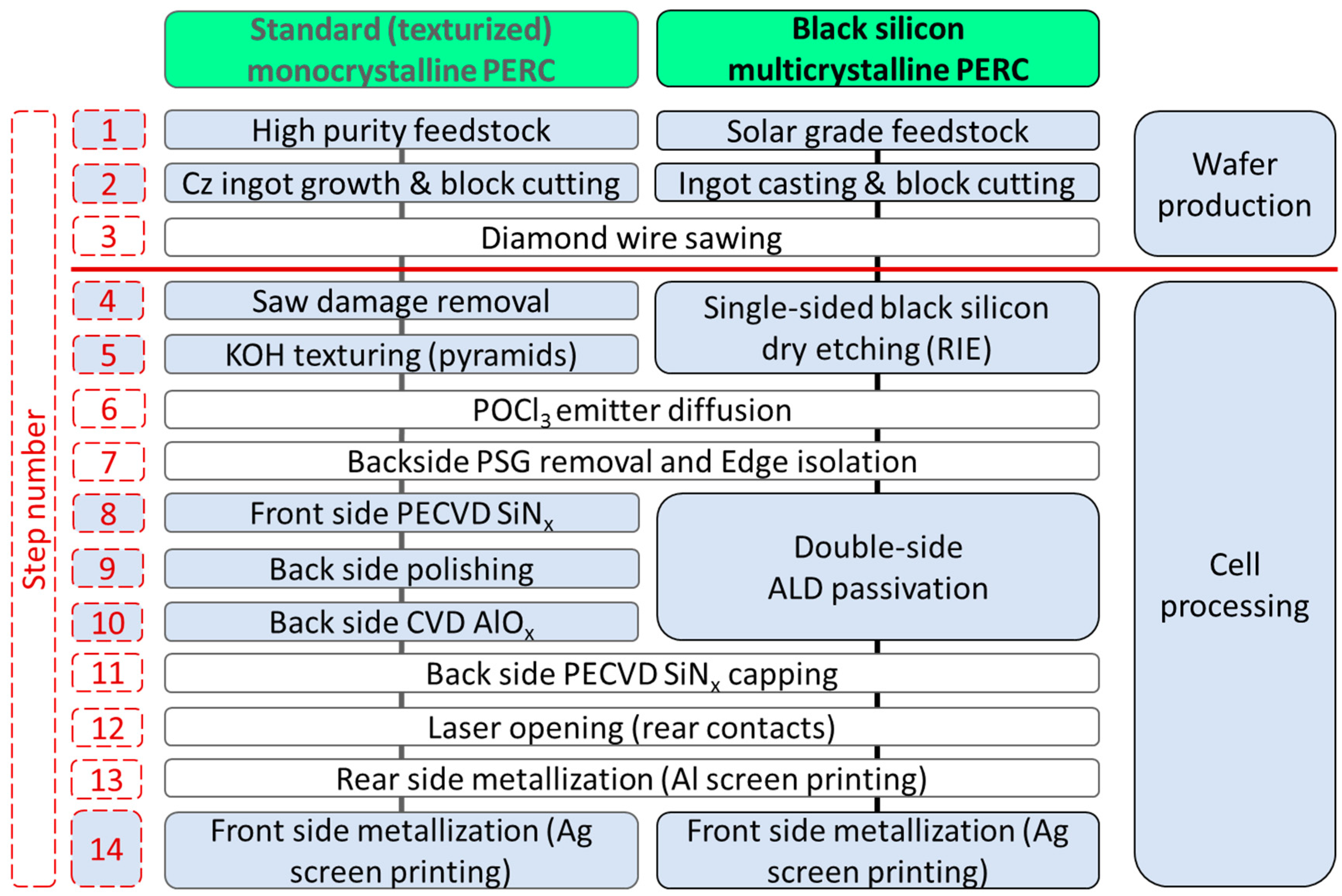
Figure 2.
Sum of the normalized costs for the PERC process steps for the reference device (standard texturized Czochralski PERC).
Figure 2.
Sum of the normalized costs for the PERC process steps for the reference device (standard texturized Czochralski PERC).

Figure 3.
Sum of the normalized costs for the PERC process steps for the b-Si multicrystalline PERC. Step costs are normalized over the total costs for the reference device (standard texturized Czochralski PERC). Note the smallest contribution value is rounded up to 0.1% to be visible.
Figure 3.
Sum of the normalized costs for the PERC process steps for the b-Si multicrystalline PERC. Step costs are normalized over the total costs for the reference device (standard texturized Czochralski PERC). Note the smallest contribution value is rounded up to 0.1% to be visible.
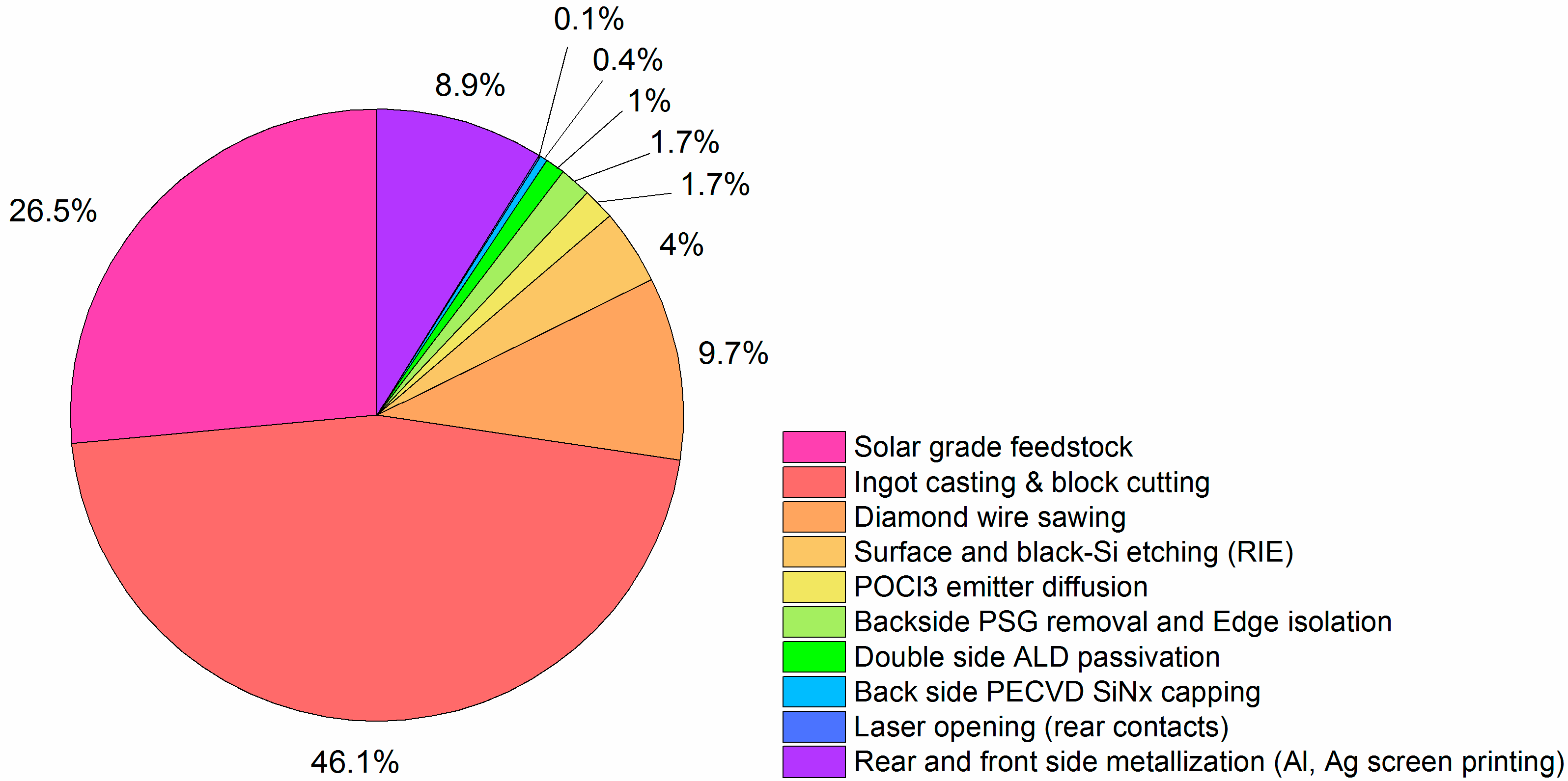
Figure 4.
Sum of the normalized costs for the PERC process steps that are different between the reference (standard texturized Cz-Si PERC) and the black mc-Si PERC. Step costs are normalized over the total steps costs for the reference device. The numbers on the black mc-Si PERC show the multiplying factor for each step in the process compared to the reference for the given process step.

Figure 5.
The cost per unit of solar photovoltaic cell power ($/W) as a function of cumulative global PV production in GW.
Figure 5.
The cost per unit of solar photovoltaic cell power ($/W) as a function of cumulative global PV production in GW.

© 2018 by the authors. Licensee MDPI, Basel, Switzerland. This article is an open access article distributed under the terms and conditions of the Creative Commons Attribution (CC BY) license (http://creativecommons.org/licenses/by/4.0/).
Share and Cite
MDPI and ACS Style
Modanese, C.; Laine, H.S.; Pasanen, T.P.; Savin, H.; Pearce, J.M. Economic Advantages of Dry-Etched Black Silicon in Passivated Emitter Rear Cell (PERC) Photovoltaic Manufacturing. Energies 2018, 11, 2337. https://doi.org/10.3390/en11092337
AMA Style
Modanese C, Laine HS, Pasanen TP, Savin H, Pearce JM. Economic Advantages of Dry-Etched Black Silicon in Passivated Emitter Rear Cell (PERC) Photovoltaic Manufacturing. Energies. 2018; 11(9):2337. https://doi.org/10.3390/en11092337
Chicago/Turabian StyleModanese, Chiara, Hannu S. Laine, Toni P. Pasanen, Hele Savin, and Joshua M. Pearce. 2018. "Economic Advantages of Dry-Etched Black Silicon in Passivated Emitter Rear Cell (PERC) Photovoltaic Manufacturing" Energies 11, no. 9: 2337. https://doi.org/10.3390/en11092337
Note that from the first issue of 2016, this journal uses article numbers instead of page numbers. See further details here.