Article

Extraction of Junction Temperature of SiC MOSFET Module Based on Turn-On dIDS/dt

1
School of Electrical and Power Engineering, China University of Mining and Technology, Xuzhou 221116, China
2
Xuzhou China Ming Driver and Automation Co. Ltd., Xuzhou 221112, China
*
Author to whom correspondence should be addressed.
Energies 2018, 11(8), 1951; https://doi.org/10.3390/en11081951
Submission received: 12 June 2018 / Revised: 25 July 2018 / Accepted: 26 July 2018 / Published: 27 July 2018

Abstract

:
In this paper, a method of extracting the junction temperature based on the turn-on current switching rate (dIDS/dt) of silicon carbide (SiC) metal-oxide semiconductor field effect transistors (MOSFETs) is proposed. The temperature dependence of dIDS/dt is analyzed theoretically, and experimentally to show that dIDS/dt increases with the rising junction temperature. In addition, other factors affecting dIDS/dt are also discussed by using the fundamental device physics equations and experiments. The result shows that the increase of the DC-link voltage VDC, the external gate resistance RG-ext, and the decrease of the driving voltage VGG can increase the temperature sensitivity of the dIDS/dt. A PCB (printed circuit board) Rogowski coil measuring circuit based on the fact that the SiC MOSFET chip temperature and dIDS/dt is estimated in a linear way is designed to obtain the junction temperature. The experimental results demonstrate that the proposed junction temperature extracting is effective.

1. Introduction

In recent years, power semiconductor devices such as the insulated gate bipolar transistor (IGBT) and the metal-oxide semiconductor field effect transistors (MOSFETs) have been widely applied in many industrial fields especially fields with high reliability requirements in new energy, wind power generation, and automotive and aerospace industries [1]. Therefore, the reliability issues have become the focus of increasing concern. In particular, the novel wide band gap (WBG) devices, which are high electron mobility transistors such as silicon carbide (SiC) power MOSFET or gallium nitride (GaN), can significantly improve power density and conversion efficiency. However, due to the lack of related technology and the instability of the gate oxide layer, the WBG devices require significant condition monitoring to ensure its reliability [2,3,4]. Studies have shown that 31% of failures in power electronic converters can be attributed to the failure of power devices while 60% of device failures are due to thermal stress. In fact, due to the different thermal expansion coefficients of several materials in power semiconductor modules, the accumulation of thermal stress will eventually lead to aging failure. In an actual operating condition, the higher the junction temperature is, the smaller the safety margin of the operation is. Additionally, the greater the junction temperature fluctuations are, the shorter the life of the thermal cycle is. Therefore, the measurement or estimation of junction temperature is essential for its condition monitoring [5,6]. Obtaining this temperature in real time during the operation of the converter can effectively improve the status monitoring system of the SiC MOSFET. In addition, using the junction temperature-based control algorithm can enhance the lifetime of the module [7].
The current methods for obtaining the power semiconductor junction temperature are mainly through a direct measurement method and an indirect measurement method. Direct measurement methods are based on optical and physical contact methods that use infrared cameras (IR) and thermocouples to measure the junction temperature, but they need to destroy the module package structure [8,9]. This method uses an internal implanted thermistor sensor to obtain temperature, but it is limited by the accuracy and bandwidth of the sensor and the dynamic response is slow (a few milliseconds are required). This means the methods based on optical and physical contact are limited in practical industrial applications. Indirect measurement methods mainly include the RC thermal impedance model [10,11] and the thermo-sensitive electrical parameter (TSEP). The RC thermal resistance network model mainly includes the Foster and Cauer models, but they do not consider changes in the thermal impedance caused by aging, which results in the inability to obtain accurate junction temperatures. Based on the TSEP, the temperature estimation of the standard package module can be performed non-invasively without modifying the module itself and only the electrical parameters of the device need to be obtained. Many studies have found that the TSEP method is the most promising solution for monitoring the junction temperature of the module [12]. The high-precision and fast-response temperature measurement of the power device can be performed, and the junction temperature can be measured online or offline using TSEP. This is a very extensive research field. Reference [13] uses the on-resistance Ron to obtain the junction temperature of the IGBT. However, due to the low on-resistance of the SiC MOSFET (several tens of mΩ), a very precise measurement circuit is required and the switching frequency of the SiC MOSFET is high. It is difficult to measure the junction temperature accurately. In Reference [14], the IGBT junction temperature was measured using the Miller plateau voltage (VGP). However, due to the high switching speed of the SiC MOSFET, the turn-on transient is only few hundred nanoseconds, which means the length of the Miller platform is very short and is difficult to measure. Reference [15] provides a method for measuring the junction temperature using the threshold voltage (VTH) of the IGBT. Physically, VTH is the minimum gate bias inducing an inversion layer of free electrons underneath the gate oxide. It creates a conductive channel between the drain and source in MOSFET or the collector and emitter in IGBT. Since this voltage is not well defined, a quasi-threshold voltage (gate voltage of drain current reaching 10% of rated current) can only be obtained by detecting the value of the drain current. Reference [16] uses the turn-off delay of IGBT to measure the junction temperature, but SiC MOSFET is a unipolar switching device and does not include any extracting minority carriers during the turned off transient. Therefore, the junction temperature cannot be measured using the temperature sensitivity of the minority carrier during the turn off transient. Reference [17] proposed a method to obtain the junction temperature based on the peak value of the gate current IG peak during the SiC MOSFET turn-on transient. Based on the positive temperature coefficient of the internal gate resistance (RG-in), SiC MOSFET can generate different gate currents at different temperatures. The junction temperature is extracted by obtaining the peak value of the gate current.
Reference [18] includes an analysis of the relationship between dIDS/dt and the junction temperature during the SiC MOSFET turned on and off transient. However, it lacks the experimental research on the large current module and does not design a measurement circuit to define the junction temperature. In summary, compared to silicon semiconductors, there are few studies on the junction temperature of silicon carbide semiconductors. Due to the wide bandgap characteristics of SiC MOSFET, some methods of extracting junction temperature can be used on silicon IGBT but cannot be applied to SiC MOSFET. In this paper, based on the switching characteristics of SiC MOSFET, the junction temperature is obtained by the turn-on current switching rate (dIDS/dt). Firstly, it is analyzed that the temperature sensitivity of dIDS/dt is mainly related to the negative temperature coefficient of the threshold voltage (VTH). Second, an experimental platform was established to demonstrate the good linear relationship between dIDS/dt and the junction temperature. The effects of gate drive resistance RG, the supply voltage VDC, load current IDS, and the drive voltage VGG on dIDS/dt have been experimentally verified. Lastly, a small and economical Rogowski coil measuring circuit for obtaining the dIDS/dt is proposed. The circuit can be embedded in the SiC MOSFET driver. The feasibility of the circuit to obtain the junction temperature is verified by experiments. In practical engineering applications, considering the switching loss and frequency, an intelligent driver method is proposed to measure the junction temperature of the SiC MOSFET without increasing the switching loss.

2. Theoretical Analysis of Turn-On dIDS/dt Temperature Dependence

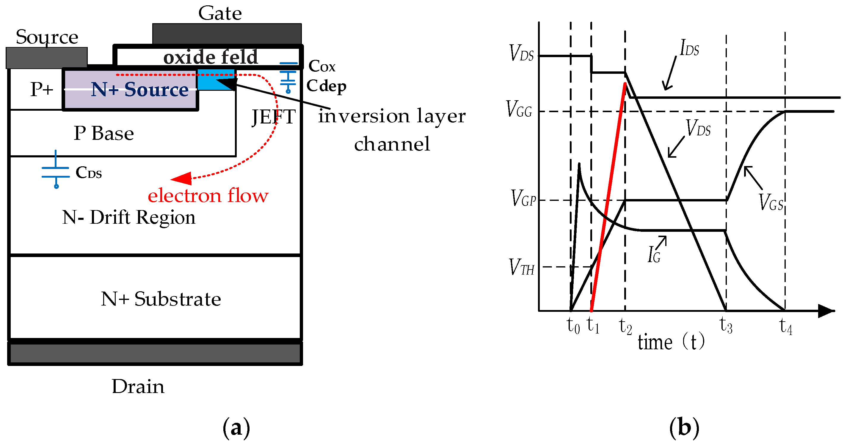
Figure 1a shows the cell structure of the planar SiC MOSFET. It can be seen that the cell of the SiC MOSFET is mainly composed of the gate, source, drain, oxide layer, N-drift region, N-base region, and Junction Field-Effect Transistor (JEFT) region. The figure also shows the route of the electron carrier flow, the position of inversion layer channel, and the distribution of parasitic capacitance.
Figure 1b shows the typical SiC MOSFET turn-on transient waveforms under an inductive load. In order to facilitate the theoretical analysis, the parasitic inductance of the switching loop is neglected [19]. This switching process can be divided into four phases to analyze further. Before t0, SiC MOSFET is blocked, the driving voltage VGG = Uoff, the drain-source voltage VDS = VDC (DC-link voltage), and the gate current IG is zero.
In Phase 1 (t ∈ [t0,t1]), the turn-on pulse trigger at t0, the driving voltage VGG = Uon, and the gate current IG first performs a step to its maximum value and then starts to decay. At the same time, the gate voltage VGS begins to increase. Due to the forward bias of VGS, holes in the P base region are first squeezed out to form a depletion layer. With the increase of VGS, the electrons (minority carriers) in the P base region begin to gather under the gate oxide layer to form an inversion layer channel when the energy band is bent to the surface potential, which is equal to the body potential. VGS rises to the threshold voltage VTH when the inversion layer channel is formed at t1. tTH is the turn-on delay time. When initiating the turn-on until VGS reaches VTH, it can be calculated by using Equation (1) where RG is the gate total resistance and CISS is the input capacitance. The expression for VTH can be obtained from reference [18] where q is the charge constant, VFB is the flat-band voltage (related to the oxide layer and semiconductor interface charge and gate material), ξsic is the dielectric constant of the semiconductor, and NA is the doping concentration. COX is the oxide layer capacitance, T is the absolute temperature (thermodynamic temperature), the Fermi potential ΨB is the potential difference between the mid-gap and the Fermi level far from the surface, and К is the Boltzmann constant.
t T H = t 1 t 0 = R G C I S S ln ( V G G V G G V T H )
V T H = V F B + 2 ψ B + 4 ξ s i c K T · N A ln ( N A / n i ) C O X
ψ B = K T q ln ( N A n i )
Using Equation (3), it can be seen that ΨB is related to the doping concentration and temperature of the semiconductor and ni is the concentration of the carrier. If the start time of turn-on is 0, the changing rate of the gate voltage can be calculated by using the equation below.
d V G S d t = V G G R G C I S S e t R G C I S S
Phase 2 (t ∈ [t1,t2)) is the inversion layer channel established at time t1. The electron carriers start to enter in the JFET region and the drain-source current IDS starts to increase. When IDS reaches the rated current, the freewheeling diode starts to reverse recovery and the IDS reaches its maximum value at time t2. Due to the influence of the parasitic inductance between the drain and source, the drain-source voltage VDS drops by a small step, but since VDS >> (VGGVTH), SiC MOSFET is in the saturation region, which means the expression of the drain current IDS can be calculated by using the following equation:
I D S = β 2 ( V G S ( t ) V T H ) 2
β = W C H μ C H · C O X L
In the above equations, β is the gain coefficient, WCH is the channel width of the inversion layer, μCH is the effective mobility of the channel electrons, COX is the capacitance of the oxide layer, and L is the channel length. The current switching rate dIDS/dt can be calculated together with Equation (4) and the derivative of Equation (5), which is shown below.
d I D S d t = β ( V G S V T H ) V G G R G C I S S e t R G C I S S
In Phase 3 (t ∈ [t2,t3)), when the drain-source current IDS reaches the maximum value at time t2, the gate voltage VGS rises to the Miller plateau voltage VGP, VGS remains basically unchanged, and IDS starts to fall to the rated current. After the reverse recovery of the freewheeling diode is complete, the gate current IG charges to the Miller capacitance reversely. At the same time, the drain-source voltage VDS begins to drop and drops to a very low on-state voltage at t3. The Miller plateau stage ends.
In Phase 4 (t ∈ [t3,t4)), the gate capacitance CGS is charged by the gate current IG after t3. VGS starts to increase exponentially and rises to the driving voltage VGG at t4. In addition, IG decreases to zero. At the end of this phase, the SiC MOSFET is fully turned on.
From the SiC MOSFET turn-on process, it can be seen that temperature-related factors include the threshold voltage VTH and the drain current change rate dIDS/dt. When Equations (2) and (3) are combined, the temperature is derived to obtain Equation (8). From Equation (2), the threshold voltage VTH is a function of temperature. As the temperature is raised, the band bending (2ΨB) required to induce an inversion layer decreases due to the rapid increase in the intrinsic carrier concentration (ni) in Equation (3). This is partially offset by the temperature pre-factor (KT) and the increased ionization of acceptors NA when the temperature is raised. However, as the temperature rises, the Fermi level moves closer to the mid-gap. Therefore, the band bending (2ΨB) needed to reach the threshold decreases. This reduces the threshold voltage, which is shown in Equation (2) [20]. Therefore, the threshold voltage decreases with an increasing temperature and shows a negative temperature coefficient.
d V T H d T = d ψ B d T ( 2 + 2 C O X ξ s i c q N A ψ B )  
The derivation of the temperature is obtained by using Equation (7).
d 2 I D S d t d T = V G G R G C I S S e t R G C I S S ( d β d T ( V G S V T H ) β d V T H d T )
From Equation (9), it can be concluded that the temperature coefficient of dIDS/dt is related to the gate threshold voltage VTH and the temperature coefficient of the gain coefficient β. Based on Equation (6), the gain coefficient β is proportional to the channel width WCH, the effective mobility of the channel μCH, and the oxide capacitance COX, but is inversely proportional to channel length L. WCH, μCH, and COX are related to the manufacturer’s process and are constant under the same module, which means β only relates to μCH. In the silicon semiconductor, μCH is about half of the mobility of the drift region while, in 4H-SiC, μCH is only 5–10% of the mobility of the drift region. It is mainly affected by the surface roughness scattering, Coulomb scattering, and phonon scattering of the semiconductor and oxide interfaces [21]. The main effect of μCH is Coulomb scattering at room temperature. As the temperature increases, the surface roughness scattering and Coulomb scattering decrease and a large number of phonon scattering increases, which results in a decrease of the carrier mobility. Therefore, μCH decreases with an increasing temperature. From Equation (6), β displays a negative temperature coefficient, but due to the wide bandgap characteristics of SiC MOSFET, μCH is very low and the temperature sensitivity of β is also low. Therefore, the negative temperature coefficient of VTH dominates the negative temperature coefficient of β [21]. The temperature coefficient of dIDS/dt ((dIDS)2⁄(dt·dT)) is mainly affected by the threshold voltage VTH.
Reference [22] proposed that the input capacitor CISS is also affected by the temperature because CISS includes Miller capacitance and gate capacitance CGS where the gate capacitance CGS does not change with temperature. The Miller capacitance is composed of the oxide layer capacitance COX and depletion layer capacitance Cdep. In general, COX does not change with the temperature. The expression of Cdep is shown in the equation below.
C d e p = A ξ s i c q N A N D 2 V D S ( N A + N D )
In Equation (10), A is the effective area of the capacitor area, ξsic is the dielectric constant, q is the unit charge, ND, NA is the doping concentration of the donor and acceptor, and VDS is the drain voltage of SiC MOSFET. When the temperature rises, the doping concentration increases, and the Miller capacitance increases with a rise in temperature. It shows a positive temperature coefficient. However, since the rise of the drain-source current IDS mainly occurs in Phase 2 (t1, t2), the drain voltage VDS is large during this period, which means the depletion capacitance Cdep is small. The Miller capacitance is mainly the oxide capacitance COX [20]. Therefore, the temperature effect of the input capacitor CISS can be ignored.
In summary, due to the negative temperature coefficient of the threshold voltage (a negative sign before dVTH/dT in Equation (9)), the turn-on dIDS/dt shows a positive temperature coefficient and the SiC MOSFET turns on faster at a higher temperature.

3. Experimental Verification of dIDS/dt Temperature Dependence

3.1. Relationship between dIDS/dt and Junction Temperature

In order to demonstrate dIDS/dt temperature dependence, a 1.2 kV, 180 A SiC MOSFET module (BSM180D12P2C101, ROHM Semiconductor, Kyoto, Japan) [23] was used to build a double pulse experimental platform, which is shown in Figure 2. The module has two SiC MOSFETs switches in series including one as a test device and the other as a freewheeling diode (D1). The module has a parasitic inductance LS between source S and auxiliary source S’ and it can be seen that LS is 13 nH from the manual. In the experiment, the DC-link voltage was measured using a high-voltage differential probe (N2891A, Agilent Technologies, Santa Clara, CA, USA) and the drain current was measured using a Rogowski coil (CWTMini1B, PEM, Nottingham, UK). The oscilloscope used for capturing the data was Agilent MSO8064A with a bandwidth of 600 MHz. The SiC MOSFET module is placed on the adjustable heating plate and coated with thermal grease on the substrate. The substrate of the module is closely attached to the heating plate and each temperature is adjusted. The heating process takes a long time in order for the junction temperature (Tj) of the chip can be considered equal to the temperature of the heating plate. Each experiment is performed from a low temperature to a high temperature, which ensures that there is no heat wasted inside the chip. In addition, it improves the measurement accuracy. The experimental circuit is shown in Figure 3.
The DC-link voltage VDC = 350 V, the load inductance LLOAD = 200 μH, the external resistor RG = 60 Ω, and the driving voltage VGG = 18 V. The SiC MOSFET was tested at 60 °C, 75 °C, 100 °C, 125 °C, and 150 °C for double-pulse measurements. The drain current IDS waveforms (measured by the Rogowski coil) of several temperatures are shown in Figure 4. It can be seen that the dIDS/dt of 150 °C is greater than 60 °C. Therefore, the dIDS/dt increases when the temperature is raised due to the negative temperature sensitivity of the threshold voltage VTH. In addition, at higher temperatures, the inversion layer forms earlier and the drain-source current IDS takes the shortest time to reach the rated current. At the same time, the intrinsic carrier concentration increases with a rising temperature, more carriers flow through the channel, and dIDS/dt becomes larger. Therefore, dIDS/dt shows a positive temperature coefficient, which is consistent with the above theoretical analysis during the turn on transient. In the experiment, the voltage of the parasitic inductance LS between the auxiliary source S’ and the source S is measured, which is shown in Figure 5. It can be seen that the peak value of VS’S increases with an increasing temperature and shows a better linear relationship. The dIDS/dt can be obtained by Equation (11). The voltage VS’S is 1.6 V at 75 °C and 1.9 V at 150 °C. Therefore, it has a difference of 300 millivolts. The resolution of VS’S is 4 mV/°C and the junction temperature can be obtained in real time by using Equation (12) where K0 is the temperature resolution. This is related to the manufacturer’s production process and product type. V S S | T 0 is the VS’S value at temperature T0.
d I D S d t = V s s L S
T = K 0 ( V S S V S S | T 0 ) + T 0

3.2. Influence of Other Factors on dIDS/dt

If dIDS/dt is used as the parameter of TSEP for SiC MOSFET condition monitoring, its relationship with other parameters must be calibrated. The temperature sensitivity of dIDS/dt needs to be removed from these factors in order to be used for the junction temperature detection. From Equations (7) and (9), it is clearly shown that the factors affecting the dIDS/dt are gate resistance RG, the DC-link voltage VDC, the load current, the gate voltage VGG, and the junction temperature Tj. The relationship between them is shown in Figure 6. The current change rate dIDS/dt increases when the junction temperature Tj, the drive voltage VGG, and the DC-link voltage VDC increase. However, dIDS/dt decreases with increasing gate resistance RG. The load current cannot be determined by using the formula. The following experiments are used to verify their relationship.

3.2.1. Effect of Load Current and DC-link Voltage on dIDS/dt

The effect of the load current on the temperature sensitivity of dIDS/dt was analyzed in the double-pulse experiment, and the load current can be adjusted by changing the pulse duration of the turn-on voltage VGG. The experiments were performed at the DC-link voltage VDC = 350 V, the driving resistance RG-ext = 60 Ω, the junction temperature Tj = 150 °C, and a range of load current from 50 A to 160 A. The experimental waveform is shown in Figure 7. It can be seen that dIDS/dt did not change substantially under the different current at the same temperatures. Figure 8 shows that, at the same current, the higher the temperature is, the greater the dIDS/dt is and the better linearity is. Therefore, dIDS/dt is not disturbed by the fluctuation of the load current and it is beneficial to use it as TSEP for the junction temperature extraction of the SiC MOSFET under practical conditions.
In order to verify the effect of the DC-link voltage VDC on the SiC MOSFET, the temperature of SiC MOSFET is kept constant at 150 °C and the drain-source current IDS = 80 A at a steady state. Double-pulse experiments were performed at different DC-link voltages (100 V, 120 V, 180 V, 200 V, 250 V, and 380 V), respectively. The turn-on IDS and VDS waveforms are shown in Figure 9. It can be seen that, at the same temperature and rated current, there is only a slight increase in dIDS/dt of the DC-link voltage with a difference of 280 V. The voltage VS’S induced by parasitic inductance LS is measured and shown in Figure 10. It can be seen that the peak value of VS’S is also a slight increase with the increase of VDC, which means that dIDS/dt increases slightly with VDC. As the DC-link voltage increases, more charges are discharged in the N- drift region increasing the depletion layer width. This will also decrease the depletion layer capacitance Cdep. Based on Equation (10), it can also be seen that Cdep decreases with increasing DC-link voltage. Therefore, the Miller capacitance is reduced by increasing VDC, which, in turn, reduces the input capacitance CISS and speeds up the turn-on transient of the SiC MOSFET. However, Cdep is small in this stage (in Phase 2, the drain voltage VDS is large) and dIDS/dt shows a slight increase. However, the DC-link voltage VDC is often constant in voltage source converter applications, which means the influence of VDC on dIDS/dt is less important. The dIDS/dt temperature coefficient is usually calibrated to accommodate different DC-link voltages in a new operating environment. In addition, the slight fluctuation of the DC-link voltage has little effect on the dIDS/dt in the actual operating conditions, which also facilitates the use of the dIDS/dt as a TESP parameter for junction temperature extraction.

3.2.2. The Effect of Drive Resistance on dIDS/dt

As known in silicon MOSFETs and IGBTs, the external drive resistance (RG-ext) also affects the turn-on dIDS/dt of SiC MOSFET. In order to observe the effect of the RG-ext on dIDS/dt, the heating plates were adjusted to 50 °C, 75 °C, 100 °C, 125 °C, and 150°C, respectively. Each adjustment waits for one hour for the junction temperature of the chip to reach the set temperature. The rated current remains at 150 A and the waveforms of IDS observed from different RG-ext are shown in Figure 11. As observed from Figure 11 and Figure 12, the dIDS/dt reduces as the resistance increases and the switching speed becomes slower. Since the increase of RG-ext reduces the gate current IG, the gate voltage VGS charges slowly to the gate capacitance CGS and VGS reaches the threshold voltage for a longer time (introduced from Equation (1)). In addition, the time that VGS reaches the Miller platform voltage also becomes longer (in Phase 2), which means dIDS/dt will decrease when RG-ext increases (introduced in Equation (7)). However, a small RG-ext increases dIDS/dt, but the gate parasitic inductance cannot be suppressed in a way that reduces the temperature sensitivity of dIDS/dt by decreasing the gate voltage that reaches the chip [24]. It can be also seen from Figure 11 and Figure 12 that temperature sensitivity of dIDS/dt shows better linearity under a large RG-ext and there is less oscillation in the waveform of IDS at a large drive resistance, which creates an easy way to obtain dIDS/dt. In addition, RG-in is the equivalent of the distribution resistance of the gate polysilicon and metal connection in MOSFET. Reference [25] confirmed that RG-in shows a positive temperature coefficient. If RG-ext is large, the temperature effect of RG-in is suppressed and it can be defaulted as RG (RG = RG-ext + RG-in). This does not change with increasing temperature, which means dIDS/dt has better temperature sensitivity under larger RG-ext. Equation (9) also suggests that the increase of RG decreases the coefficient in front of dβ/dT, which increases the temperature sensitivity of dIDS/dt.
In summary, the experimental and theoretical analysis are consistent and dIDS/dt shows better temperature sensitivity under the larger RG. Based on the experiment of this module, it is found that RG-ext shows a better temperature sensitivity when it is around 60 Ω (relative to RG-in, which is already very large). Since RG-ext is so large, dIDS/dt is too small, which makes the measurement difficult.

3.2.3. Driving Voltage VGG Effect on dIDS/dt

Combined with the theoretical analysis of the second part, it can be seen from Equation (7) that the reduction of the driving voltage VGG will reduce the dIDS/dt. However, from Equation (9), it can be deduced that the decrease of VGG reduces the coefficient of dβ/dT, which increases the positive temperature coefficient of dIDS/dt. In order to verify the influence of VGG on the temperature coefficient of dIDS/dt, the DC-link voltage VDC is kept at 350 V, the driving resistance is RG-ext = 60 Ω, and IDS at a steady state is 100 A. The double-pulse experiment was performed at different driving voltages of 12 V, 15 V, 18 V, and 20 V and different temperature points of 50 °C, 75 °C, 100 °C, 125 °C, and 150 °C, respectively. Figure 13 shows the waveforms of IDS with different drive voltages of 12 V and 20 V, respectively. Figure 14 shows the dIDS/dt values for different temperatures under the four driving voltages. It can be seen from Figure 13 that, as the driving voltage decreases, dIDS/dt becomes smaller. However, there is a greater range of variation with the junction temperature when the driving voltage VGG = 12 V. Using the dIDS/dt measured at 50 °C when VGG is 12 V as a reference, the value of dIDS/dt at 150 °C increases by 1.2 times. Similarly, using the dIDS/dt measured at 50 °C when VGG = 20 V as a reference, the value of dIDS/dt at 150 °C increases by 1.12 times. At the same time, the reduction of VGG reduces the switching speed and the oscillation of IDS that facilitates the measurement of the dIDS/dt. Therefore, dIDS/dt shows better temperature sensitivity at low drive voltages. However, it can be seen from Figure 14 that the dIDS/dt is too low when the driving voltage is reduced, which makes it difficult to measure. In addition, if VGG is too low, the module will not be completely turned on and it will work in the active area. Therefore, it is best to select a driving voltage of 12 V based on this module.

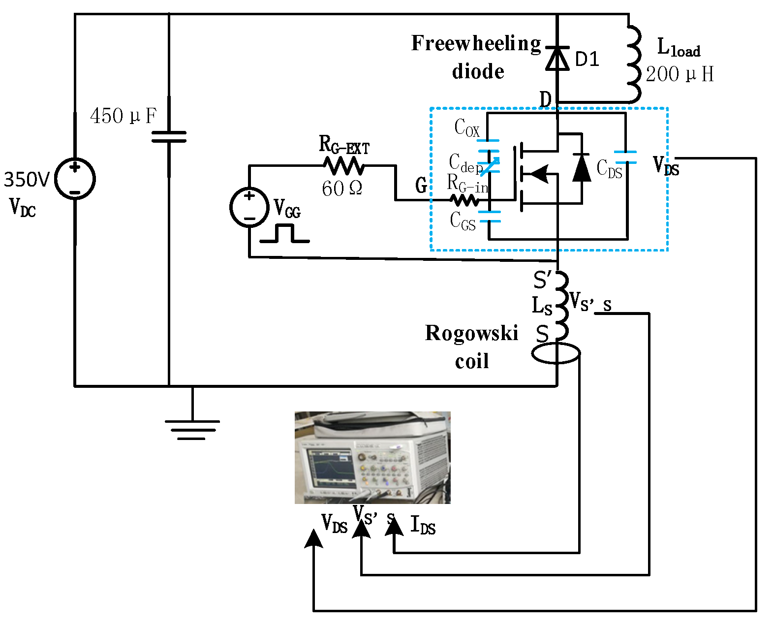
4. Design Measuring Junction Temperature Circuit and Experimental Verification

The dIDS/dt as a real-time junction temperature extraction for SiC MOSFETs can be achieved using the following method. For the SiC MOSFET module with a source auxiliary terminal S, it is possible to measure the peak value of the induced voltage VS’S generated by the parasitic inductance LS between the source assist S’ and the source S during the SiC MOSFET turn-on transient. The value of LS can be found in the device manual. According to the formula VS’S = L(dIDS/dt), the value of dIDS/dt can be obtained. Figure 15 shows the peak value measurement circuit of VS’S, but the above circuit is only suitable for SiC MOSFET modules with an auxiliary source. In order to target all modules, a measurement circuit based on the printed circuit board (PCB) Rogowski coil [26] was proposed. The measurement circuit is shown in Figure 16a. It consists of two high-precision operational amplifiers (LM7171), a diode, a storage capacitor of 4.7 nF, and a discharge resistor R1. The first LM7171 is mainly used to acquire the parameters of the dIDS/dt sensed by the PCB Rogowski coil and is used to isolate the high voltage. The second LM7171 mainly amplifies the resolution according to the actual needs. It facilitates the acquisition of the one-to-one correspondence between dIDS/dt and the junction temperature. From 
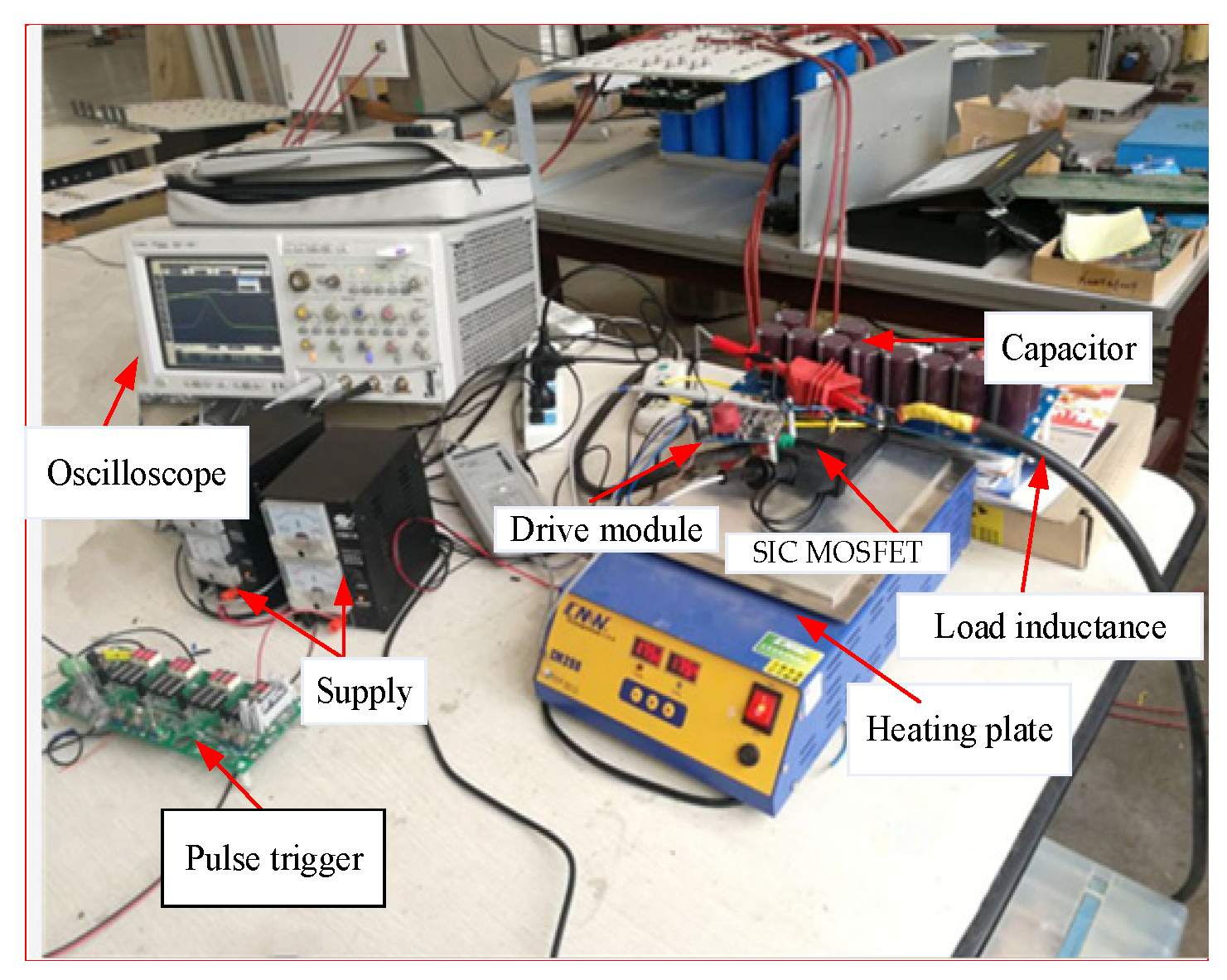
Figure 17b, it can be seen that the circuit occupies a small space and the cost is low so that it can be embedded in the drive module. The PCB Rogowski coil can be directly mounted on the terminal of the SiC MOSFET module, which offers a new idea for engineering applications.
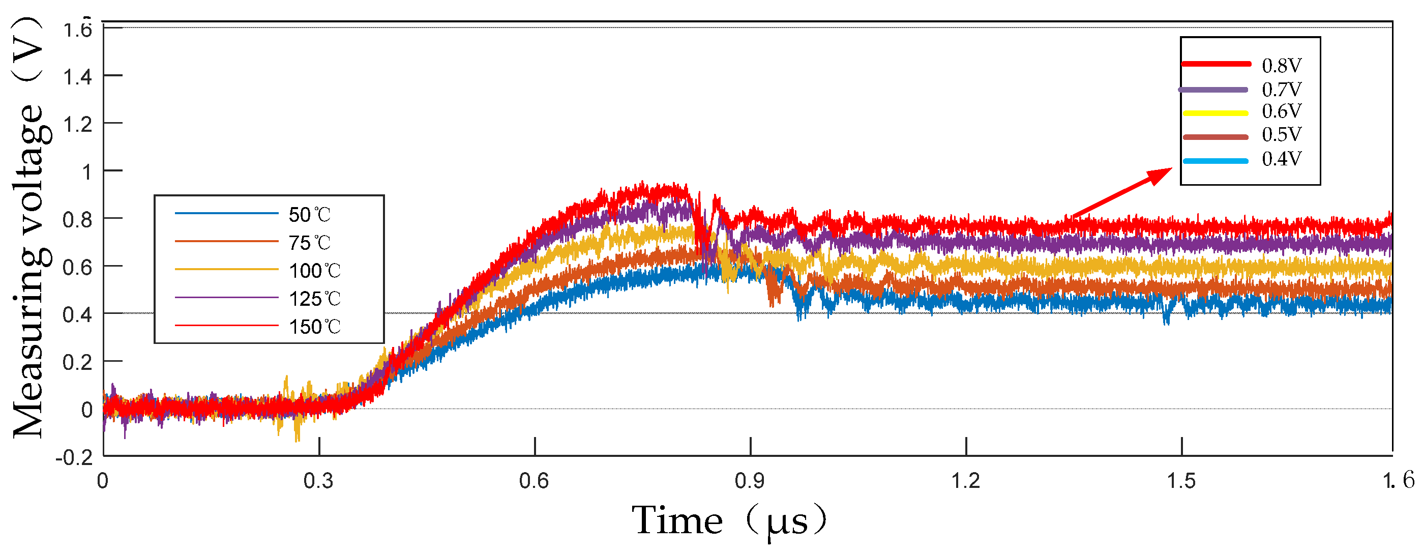
In order to verify the feasibility of the circuit, the driving voltage is 12 V under the voltage and current level of 350 V and 100 A and the double pulse experiments are carried out at the working junction temperature of SiC MOSFET at 50 °C, 75 °C, 100 °C, 125 °C, and 150 °C, respectively. The magnification of the measurement circuit is 1 (This value can be changed by adjusting the ratio of R2 to R3) and the output waveform is shown in Figure 17. It can be seen that each temperature corresponding to the measured voltage shows better linearity. The measured voltage is 0.4 V at 50 °C, and 0.8 V at 150 °C. In addition, the resolution is 4 mV/°C. The resolution can be increased by increasing the amplification of the operational amplifier. The Junction temperature of SiC MOSFET can be obtained by using Equation (13) where T1 is the calculation temperature, K1 is the resolution (250 °C/mV), and V1 is the measuring voltage by this measuring circuit.
T 1 = K 1 ( V 1 0.4 ) + 50
To further test the feasibility of extracting the junction temperature of this circuit, the heating plate is adjusted to different temperatures. The measured voltage is obtained by the measuring circuit of Figure 16 and the measured temperature can be calculated by using Equation (13). The result is shown in Table 1. It can be observed that, compared with the actual junction temperature, the maximum deviation of the calculated temperature does not exceed 5 °C. Therefore, this circuit for extracting the junction temperature of SiC MOSFET is feasible. In an actual operation, the junction temperature and the measurement voltage corresponding to the calculated temperature are converted into the digital signals by the A/D module (Analog to Digital Converter) and are stored in the Field-Programmable Gate Array (FPGA) of the driving module. The junction temperature is obtained by looking up the table.
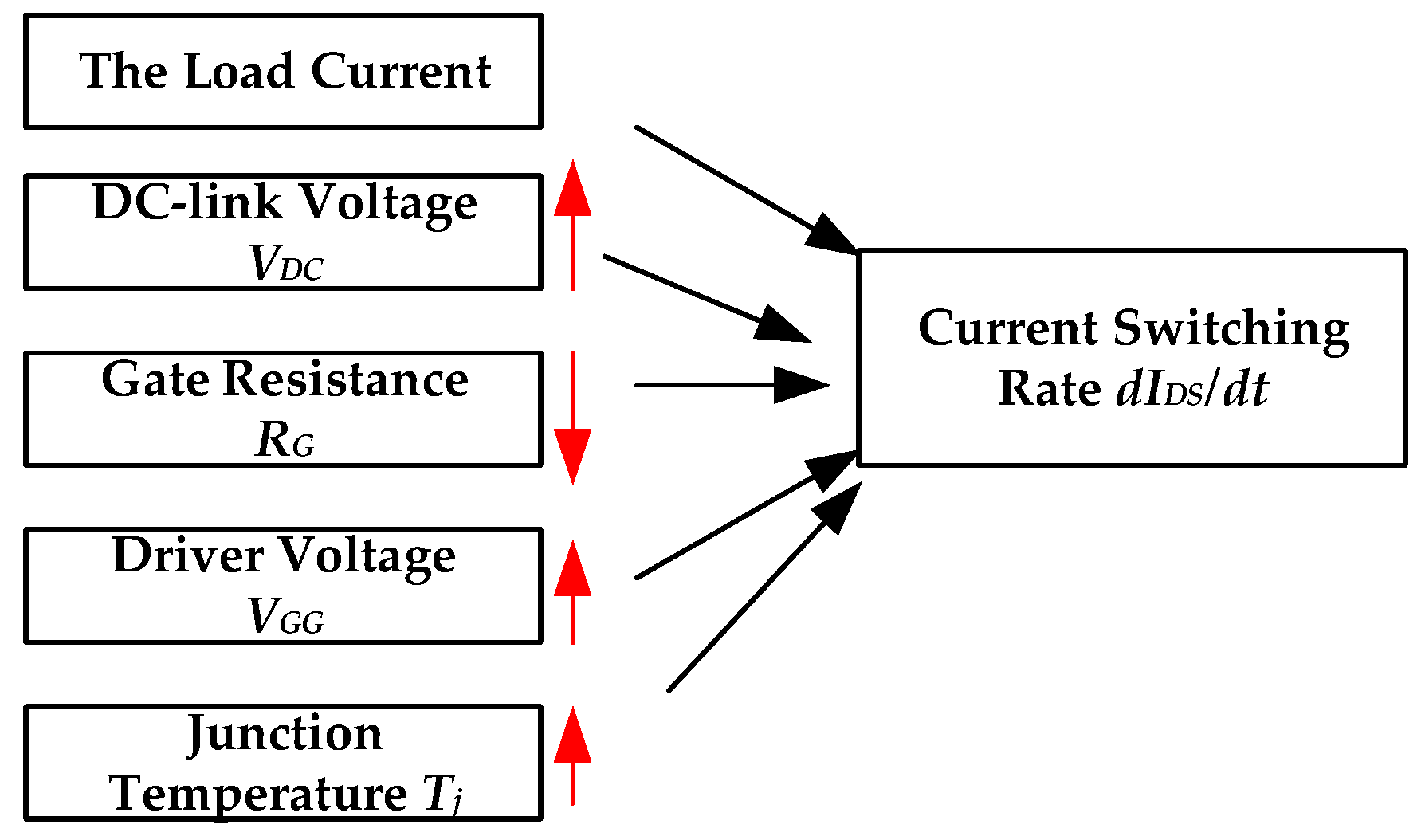
As mentioned above, dIDS/dt has better temperature sensitivity under a small drive voltage and a large drive resistance, but it also brings about an increase in the switching loss. Since the real work does not need to extract the junction temperature at every moment, an intelligent driver [27] can be used to set a small time period to make the driver open SiC MOSFET under the large resistance and small drive voltage for the junction temperature extraction. After the data is acquired, the original small drive resistance and large gate voltage are restored. Therefore, the accurate junction temperature can be extracted while satisfying fast switching frequency and small switching loss. In summary, it is feasible to extract the junction temperature from SiC MOSFET based on dIDS/dt.

5. Conclusions

In this paper, the temperature dependence of the turn-on dIDS/dt of SiC MOSFET is discussed using device mathematical models and experiments. It is shown that dIDS/dt increases with a rising temperature as a result of the negative temperature sensitivity of the threshold voltage VTH. Afterward, other factors affecting dIDS/dt are analyzed. It was found that rising DC-link voltage VDC values and external gate resistance RG-ext as well as the decrease of the driving voltage VGG can increase the temperature sensitivity of dIDS/dt. However, the load current has no effect on dIDS/dt. Therefore, there is a good temperature sensitivity of dIDS/dt under large drive resistance and small drive voltage. Lastly, a small and low-cost PCB-based Rogowski coil measurement circuit was designed. The dIDS/dt obtained by this circuit exhibits a near linear dependency on temperature with a resolution of 4 mV/°C (the resolution can be increased by adjusting the amplification factor). When the actual application needs junction temperature extraction, the intelligent driver sends a detection signal to turn on the SiC MOSFET under a small drive voltage and a large drive resistance. The value of dIDS/dt is obtained by measuring the circuit based on the PCB Rogowski coil. Afterward, the operating junction temperature of SiC MOSFET is obtained by the junction temperature database.
Future work will focus on designing intelligent drivers that can be embedded into the junction temperature detection (based on the junction temperature extraction of turn-on dIDS/dt) to use for SiC MOSFET health monitoring (the dIDS/dt temperature sensitivity of aging devices is different). This further tracks the aging of devices and provides an estimation of remaining life.

Author Contributions

G.T. and D.H. conceived and designed the experiments. D.H. and C.G. designed and performed the simulations. J.Z. performed the experiments. D.H. and C.L. wrote the paper.

Acknowledgments

The project is supported by the National key research and development program funded project (2016YF C0600804).

Conflicts of Interest

The authors declare no conflict of interest.

References

  1. She, X.; Huang, A.Q.; Lucıa, O.; Ozpineci, B. Review of silicon carbide power devices and their applications. IEEE Trans. Ind. Electron. 2017, 64, 8193–8205. [Google Scholar] [CrossRef]
  2. Manohar, S.S.; Sahoo, A.; Subramaniam, A.; Panda, S.K. Condition monitoring of power electronic converters in power plants—A review. In Proceedings of the 20th International Conference on Electrical Machines and Systems (ICEMS), Sydney, Australia, 11–14 August 2017; pp. 1–5. [Google Scholar]
  3. Agarwal, A.; Fatima, H.; Haney, S.; Ryu, S.H. A new degradation mechanism in high voltage SIC power MOSFETs. IEEE Trans. Electron Devices 2007, 28, 587–589. [Google Scholar] [CrossRef]
  4. Erturk, F.; Akin, B. A method for online ageing detection in SIC MOSFETS. In Proceedings of the 2017 IEEE Applied Power Electronics Conference and Exposition (APEC), Tampa, FL, USA, 26–30 March 2017; pp. 3576–3581. [Google Scholar]
  5. Qian, Z.; Zhang, J.; Sheng, K. Status and development of power semiconductor devices and its applications. Proc. CSEE 2014, 34, 5149–5161. (In Chinese) [Google Scholar]
  6. Mandrusiak, G.; She, X.; Waddell, A.M.; Acharya, S. On the transient thermal characteristics of silicon carbide power electronics modules. IEEE Trans Power Electron. 2018. [Google Scholar] [CrossRef]
  7. Baker, N.; Liserre, M.; Dupont, L.; Avenas, Y. Improved reliability of power modules: A review of online junction temperature measurement methods. IEEE Ind. Electron. Mag. 2014, 8, 17–27. [Google Scholar] [CrossRef]
  8. Baker, N.; Dupont, L.; Munk-Nielsen, S.; Iannuzzo, F.; Liserre, M. IR camera validation of IGBT junction temperature measurement via peak gate current. IEEE Trans. Power Electron. 2016, 32, 3099–3111. [Google Scholar] [CrossRef]
  9. Berthou, M.; Godignon, P.; Millan, J. Monolithically integrated temperature sensorin silicon carbide power MOSFETs. IEEE Trans. Power Electron. 2014, 29, 4970–4977. [Google Scholar] [CrossRef]
  10. Li, J.; Castellazzi, A.; Eleffendi, M.A.; Gurpinar, E.; Johnson, C.M.; Mills, L. A physical RC network model for electrothermal analysis of a multichip SiC power module. IEEE Trans. Power Electron. 2018, 33, 2494–2508. [Google Scholar] [CrossRef]
  11. Gachovska, T.K.; Tian, B.; Hudgins, J.L.; Qiao, W.; Donlon, J.F. A real-time thermal model for monitoring of power semiconductor devices. IEEE Trans. Ind. Appl. 2015, 51, 3361–3367. [Google Scholar] [CrossRef]
  12. Avenas, Y.; Dupont, L.; Khatir, Z. Temperature measurement of power semi- conductor devices by thermo-sensitive electrical parameters—A review. Trans. Power Electron. 2012, 27, 3081–3092. [Google Scholar] [CrossRef]
  13. Dupont, L.; Avenas, Y. Evaluation of thermo-sensitive electrical parameters based on the forward voltage for on-line chip temperature measurements of IGBT devices. In Proceedings of the 2014 IEEE Energy Conversion Congress and Exposition (ECCE), Pittsburgh, PA, USA, 14–18 September 2014; pp. 4028–4035. [Google Scholar]
  14. Van der Broeck, C.H.; Gospodinov, A.; de Doncker, R.W. IGBT junction temperature estimation via gate voltage plateau sensing. IEEE Trans. Ind. Appl. 2018. [Google Scholar] [CrossRef]
  15. Ren, L.; Shen, Q.; Gong, C. Real-time aging monitoring for power MOSFETs using threshold voltage. In Proceedings of the IECON 2016—42nd Annual Conference of the IEEE Industrial Electronics Society, Florence, Italy, 23–26 October 2016; pp. 441–446. [Google Scholar]
  16. Luo, H.; Li, W.; Iannuzzo, F.; He, X.; Blaabjerg, F. Enabling junction temperature estimation via collector-side thermo-sensitive electrical parameters through emitter stray inductance in high power IGBT modules. IEEE Trans. Ind. Electron. 2018, 65, 4724–4738. [Google Scholar] [CrossRef]
  17. Niu, H.; Lorenz, R.D. Real-time junction temperature sensing for silicon carbide MOSFET with different gate drive topologies and different operating conditions. IEEE Trans. Power Electron. 2018, 33, 3434–3440. [Google Scholar] [CrossRef]
  18. Liao, X.; Li, H.; Hu, Y.; Huang, Z.; Song, E.; Xiao, H. Analysis of SiC MOSFET dI/dt and its temperature dependence. In Proceedings of the IECON 2017—43rd Annual Conference of the IEEE Industrial Electronics Society, Beijing, China, 29 October–1 November 2017; pp. 864–869. [Google Scholar]
  19. Wang, J.; Chung, H.S.; Li, R.T. Characterization and experimental assessment of the effects of parasitic elements on the MOSFET switching performance. IEEE Trans. Power Electron. 2013, 28, 573–590. [Google Scholar] [CrossRef]
  20. Baliga, B.J. Fundamentals of Power Semiconductor Devices; Springer: New York, NY, USA, 2008; pp. 279–300. [Google Scholar]
  21. Kimoto, T.; Cooper, J.A. Fundamentals of Silicon Carbide Technology; John Wiley: Singapore, 2014; pp. 312–320. [Google Scholar]
  22. Luo, H.; Iannuzzo, F.; Blaabjerg, F.; Wang, X.; Li, W.; He, X. Elimination of bus voltage impact on temperature sensitive electrical parameter during turn-on transition for junction temperatuer estimation of high-power IGBT modules. In Proceedings of the 2017 IEEE Energy Conversion Congress and Exposition (ECCE), Cincinnati, OH, USA, 1–5 October 2017; pp. 5892–5898. [Google Scholar]
  23. Silicon Carbide Power Module-BSM180D12P2C101. Available online: https://www.rohm.com.cn/products/sic-power-devices/sic-power-module/bsm180d12p2c101-product (accessed on 27 July 2018).
  24. Ke, J.; Sun, P.; Zhang, X.; Zhao, Z.; Cui, X. Experimental study of the factors affecting on SiC MOSFET switching performance. In Proceedings of the PCIM Asia 2017, International Exhibition and Conference for Power Electronics, Intelligent Motion, Renewable Energy and Energy Management, Shanghai, China, 27–29 June 2017; pp. 1–8. [Google Scholar]
  25. Baker, N.; Munk-Nielsen, S.; Iannuzzo, F.; Liserre, M. IGBT junction temperature measurement via peak gate current. IEEE Trans. Power Electron. 2016, 31, 3784–3793. [Google Scholar] [CrossRef]
  26. Koga, M.; Tsukuda, M.; Tsukuda, M.; Nakashima, K.; Omura, I. Application-specific micro Rogowski coil for power modules—Design tool novel coil pattern and demonstration. In Proceedings of the 9th International Conference on Integrated Power Electronics Systems, Nuremberg, Germany, 8–10 March 2016; pp. 1–5. [Google Scholar]
  27. Idir, N.; Bausière, R.; Franchaud, J.J. Active gate voltage control of turn-on di/dt and turn off dv/dt in insulated gate transistors. IEEE Trans. Power Electron. 2016, 21, 849–855. [Google Scholar] [CrossRef]
Figure 1. (a) Cell Structure of planar silicon carbide (SiC) metal-oxide semiconductor field effect transistor (MOSFET) (N-channel), (b) Typical SiC MOSFET turn-on transient waveforms under an inductive load.
Energies 11 01951 g001
Figure 2. Double pulse experimental platform.
Energies 11 01951 g002
Figure 3. Experimental circuit diagram.
Energies 11 01951 g003
Figure 4. Waveforms of the drain-source current at different temperatures.
Energies 11 01951 g004
Figure 5. Parasitic inductance LS induced the voltage waveform at turn-on.
Energies 11 01951 g005
Figure 6. Effect of increasing influence factors on dIDS/dt.
Energies 11 01951 g006
Figure 7. The measured IDS turn-on current transients for different load currents (RG-ext = 60 Ω, Tj = 150 °C).
Energies 11 01951 g007
Figure 8. The values of dIDS/dt at different temperatures (RG-ext = 60 Ω).
Energies 11 01951 g008
Figure 9. The turn-on IDS and VDS waveforms at different DC-link voltages.
Energies 11 01951 g009
Figure 10. Parasitic inductance induced voltage waveforms at different DC-link voltages.
Energies 11 01951 g010
Figure 11. Drain current waveforms with different resistors.
Energies 11 01951 g011
Figure 12. The dIDS/dt under different resistances and temperatures.
Energies 11 01951 g012
Figure 13. Different temperature drain current waveforms for two drive voltages.
Energies 11 01951 g013
Figure 14. dIDS/dt values for different temperatures under four driving voltages.
Energies 11 01951 g014
Figure 15. Parasitic inductance induced the voltage VS’S measurement circuit when it is turned on.
Energies 11 01951 g015
Figure 16. (a) dIDS/dt measuring circuit based on printed circuit board (PCB) Rogowski coil; (b) measurement circuit appearance.
Energies 11 01951 g016
Figure 17. Measurement circuit output waveforms at different temperatures.
Energies 11 01951 g017
Table 1. The measured voltage by the measuring circuit at different temperatures and the temperature calculated by using Equation (13).
Junction Temperature60 °C70 °C110 °C130 °C140 °C
Measured Voltage0.43 V0.5 V0.655 V0.73 V0.755 V
Calculation Temperature57.5 °C75 °C114 °C133 °C139 °C
Deviation−2.5 °C5 °C4 °C3 °C−1 °C

