1. Introduction
Renewable clean energy sources, wind energy, and solar photovoltaic (PV) energy, have been developed and researched to produce the clean energy to overcome the exhaustion of fossil fuels and electric vehicles and hybrid electric vehicles are developing to reduce environmental pollution and climbing temperature issues. Direct current (dc) microgrid systems have developed in order to incorporate energy storage systems, PV power, wind power, utility systems, local residential homes, and industrial factories with a common dc voltage. The dc bus voltage on the dc microgrid system can be 1500, 750, or 380 V for traction system, light rail transit, or residential building applications. Power transformers are widely employed to provide electrical isolation and voltage conversion levels. However, line frequency transformer [
1,
2] has a bulky size especially at traction and light rail applications. A high-performance dc–dc converter with high frequency and galvanic isolation is demanded as the interface between dc bus voltage and output voltage in light rail transportation vehicles. To prevent using low frequency transformer in traction and light rail applications, one possible solution is the transformerless converters [
3,
4,
5,
6] with series-parallel combination to reduce semiconductor blocking-voltage capability and current rating. The high frequency transformers are used in transformerless topologies to achieve electrical insulation demand. Conventional full-bridge dc–dc circuits use the insulated gate bipolar transistors (IGBT) devices with 1200 V voltage rating for high input voltage applications. Three-level converters [
7,
8,
9] based on high frequency Metal-Oxide-Semiconductor Field-Effect Transistor (MOSFET) power semiconductors were widely used in modern power converters to overcome low frequency problem of IGBT-based full-bridge converters. Soft switching dc–dc converters [
10,
11,
12,
13] have been studied and presented to realize high efficiency power circuits. Phase-shift duty-cycle controls have been successfully used in full-bridge dc–dc converters to have the benefits of no switching loss at heavy load and low switching losses at light load. However, the low circuit efficiency and high circulating current loss at light load are the main disadvantages. Half-bridge resonant converters have the benefits of no switching loss for all power active devices and low reverse recovery loss for fast recovery diodes. However, half-bridge resonant converters are difficult to apply in high voltage input products. Full-bridge multilevel resonant circuit [
13] was proposed to lessen voltage rating of power semiconductors and realize high efficiency converter. However, the control strategy is very difficult to implement using the general commercial integrated circuit with cost issue.
This paper studies a cascade resonant dc–dc circuit with a transformer for dc transportation vehicles. Due to series connection of two resonant circuits at input side, power semiconductors with low blocking-voltage and low turn-on resistance MOSFETs instead of Insulated Gate Bipolar Transistors (IGBTs) can be adopted to decrease conduction losses and lessen voltage rating of power active devices. Two half-bridge circuits are controlled with frequency modulation. The adopted series-connected resonant converter is operated under inductive load. Therefore, power active devices can be easily turned on under zero-voltage and fast recovery diodes are turned off under zero-current without reverse recovery current loss. Two half-bridge resonant circuits use the sane isolated transformer to lessen primary root-mean-square currents and conduction losses on active devices. The circuit schematic and system analysis are discussed in
Section 2. The converter characteristics in steady state, design procedure and test results are discussed and presented in
Section 3, followed by the conclusions.
2. Proposed Circuit and System Operation
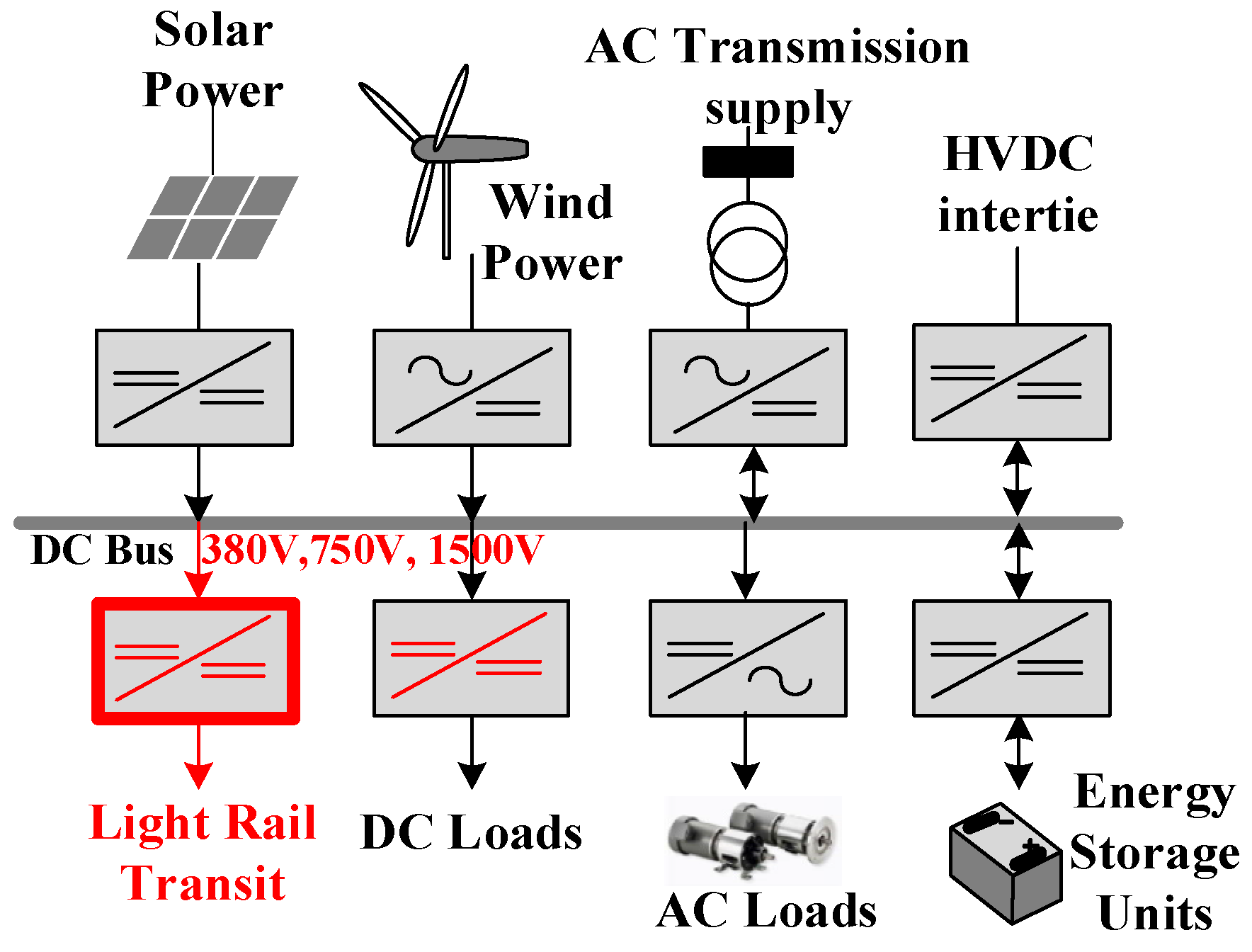
The simplified circuit blocks in a dc microgrid system are shown in
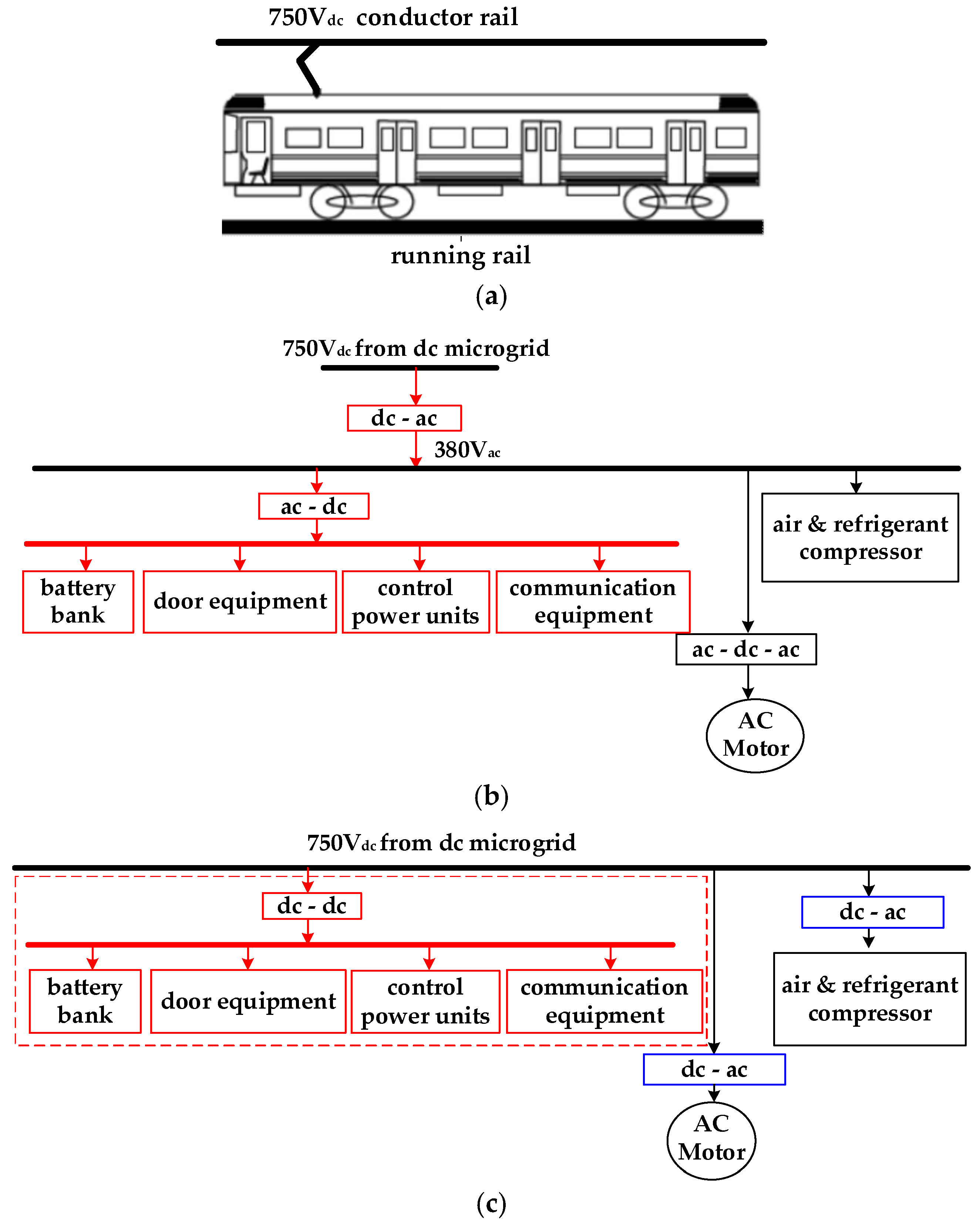
Figure 1 to combine clean energy sources, energy storage systems, utility systems, residential loads, and industrial applications. Ac–dc converters with bidirectional power flow are adopted between utility power and dc microgrid. Bidirectional dc–dc converter is adopted between dc microgrid and energy/power storage systems. For residential or commercial loads, unidirectional dc–dc converter or dc to ac converter is adopted to supply low dc voltage output or ac voltage output. The dc bus voltage in dc microgrid systems supplies 1500 V or 750 V for dc transportation systems and 380 V for local residential houses and industry factories. This study focused on dc–dc power converters for light rail transit systems. The dc microgrid for light rail applications is shown in
Figure 2a. The input voltage 750 V
dc is supplied from dc microgrid to conductor rail for power demand in each transportation vehicle. The simplified circuit diagrams of the distributed power in conventional transportation vehicles and trams. A dc– ac inverter is first used to convert input dc voltage into three-phase ac voltage. Second, an ac–dc converter converts ac voltage into low dc voltage for auxiliary power demand and an ac–dc–ac converter is adopted for ac motor drive.
Figure 2c shows the distributed power in the studied light rail transportation system. In this system, a dc–dc converter is directly converting 750 V voltage to supply auxiliary power in transportation vehicles. The dc–ac converters are adopted to drive AC motor and air and refrigerant compressors. In this way, the ac–dc converters are not necessary.
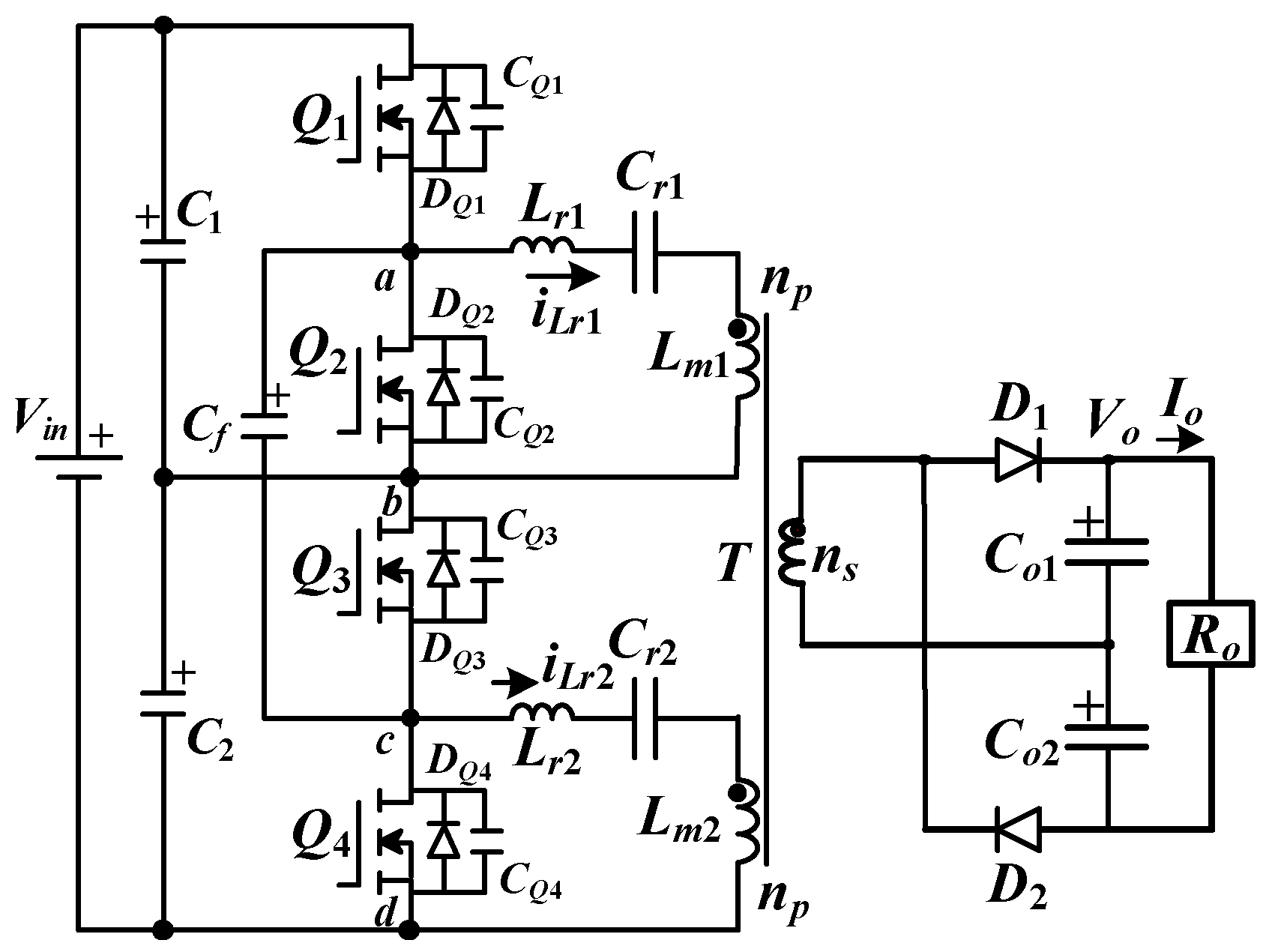
The circuit schematic of the developed converter for auxiliary circuit in light rail transportation system is given in
Figure 3. Two half-bridge circuits by input-series output-parallel connected transformer is used in the studied converter. Since two resonant circuits are series connection, the voltage rating of power devices
Q1~
Q4 is reduced. The low turn-on resistance and high frequency operation of power semiconductors such as MOSFETs are selected to decrease conduction losses and reduce converter size. A voltage balance capacitor
Cf is adopted in order to balance
VC1 and
VC2. The resonant tanks (
Lr1,
Cr1, and
Lm1) and (
Lr2,
Cr2, and
Lm2) are resonant to help power active devices with zero-voltage switching and fast recovery diodes with zero-current switching. Thus, the power losses are reduced in the studied circuit. The driving signals of half-bridge circuits are based on frequency modulation to adjust AC voltage gain and to operate at inductive load.
Figure 4 illustrates the main current and voltage signals in the studied circuit. The converter operation are based on the assumptions: (1) output capacitors
Co1 and
Co2 are larger enough to treat as the constant voltages; (2)
Q1~
Q4,
D1 and
D2 are all ideal; (3)
Cr1 =
Cr2,
Lr1 =
Lr2, and
Lm1 =
Lm2; (4)
VC1 =
VC2; and (5) the resonant tanks are operated at inductive load.
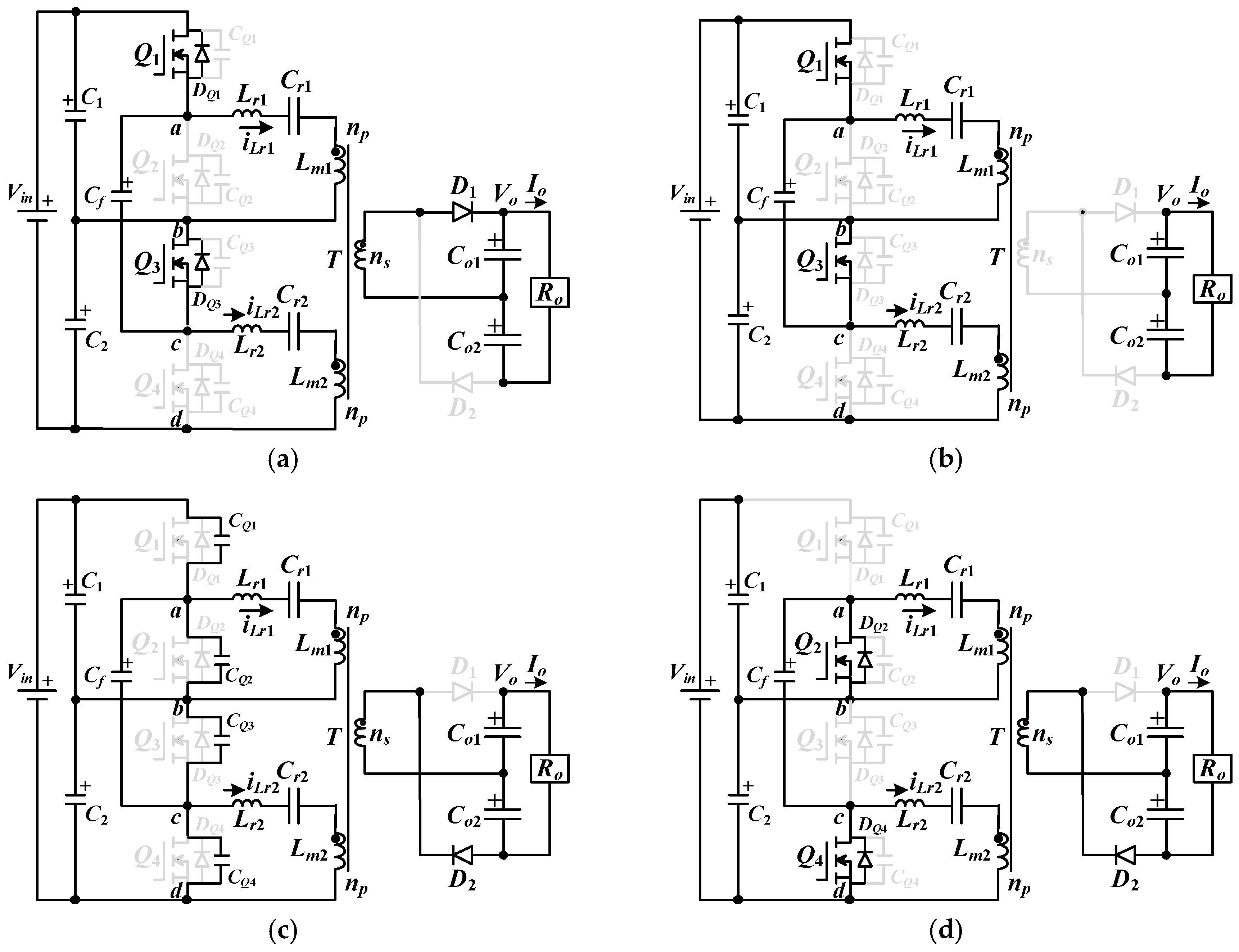
Figure 5 demonstrates the topological circuits according to the conducting states of power devices under
fsw (switching frequency) <
fr (series resonant frequency). If
fsw >
fr, then only modes 1, 3, 4, and 6 are operated in this region.
Mode 1 [
t0~
t1]: The voltages of
CQ1 and
CQ3 are reduced to zero at
t0. Then, the body diodes
DQ1 and
DQ3 conduct. Thus,
Q1 and
Q3 can be turned on to achieve zero voltage. In mode 1,
Q1,
Q3, and
D1 conduct and
VC1 =
VCf. The primary voltages
vns =
VCo1 =
Vo/2 and the primary voltages
vnp = (
np/
ns)
Vo/2 =
nVo/2. Therefore, the slope of the magnetizing currents,
diLm1/
dt and
diLm2/
dt, increases with
nVo/(2
Lm), where
Lm =
Lm1 =
Lm2. The relationships of the primary currents and the secondary current are
n(
iLr1 +
iLr2 −
iLm1 −
iLm2) =
iD1. Since
Cr1 =
Cr2,
Lr1 =
Lr2,
Lm1 =
Lm2 and
VC1 =
VC2, it can obtain
iLm1 =
iLm2 and
iLr1 =
iLr2 =
iD1/(2
n) +
iLm. In this mode, (
Lr1 and
Cr1) and (
Lr2 and
Cr2) are resonant with
Cr =
Cr1 =
Cr2 and
Lr =
Lr1 =
Lr2.
where
,
,
vCr =
vCr1 =
vCr2 and
iLr =
iLr1 =
iLr2. When the magnetizing currents
iLm1 and
iLm2 increase and equal
iLr1 and
iLr2 at time
t1. Diode
D1 becomes reverse biased.
Mode 2 [
t1~
t2]: At
t1,
iD1 = 0 and
D1 is reverse biased.
iLr1 flows through
C1,
Q1,
Lr1,
Cr1, and
Lm1, and
iLr2 flows through
C2,
Q3,
Lr2,
Cr2, and
Lm2. Since
C1 >>
Cr1 and
C2 >>
Cr2,
Lr1,
Cr1 and
Lm1 are resonant, and
Lr2,
Cr2, and
Lm2 are resonant.
where
and
.
Mode 3 [t2~t3]: At t3, active devices Q1 and Q3 turn off. iLr1(t2) will charge CQ1 and discharge CQ2, and iLr1(t2) will charge CQ3 and discharge CQ4. During this time interval, D2 conducts and vLm1 = vLm2 = −nVo/2. Since CQ1~CQ4 are so small, the time interval is neglected and iLr1 and iLr2 are considered constant.
Mode 4 [
t3~t4]: This mode starts at
t3 if
vCQ1 =
vC1,
vCQ3 =
vC2 and
vCQ2 =
vCQ4 = 0. Due to
iLr1(
t3) > 0 and
iLr2(
t3) > 0,
DQ2 and
DQ4 conduct. Therefore, active devices
Q2 and
Q4 turn on after
t3 to have the characteristic of zero voltage turn-on operation. In this mode,
vCf =
VC2. Since
D2 is forward biased,
vLm1 = vLm2 = −nVo/2 so that
iLm1 and
iLm2 decreases.
vCr1,
vCr2,
iLr1, and
iLr2 in mode 4 are calculated in (5) and (6).
When iLm1 = iLr1 and iLr2 = iLm2 at time t4. Diode D2 is reverse biased.
Mode 5 [t4 ≤ t < t5]: After t4, D2 is reverse biased and vCf = VC2. iLr1 flows through Q2, Lr1, Cr1, and Lm1, and iLr2 flows through Q4, Lr2, Cr2; Lm2. Lr1, Cr1, and Lm1 are resonant; and Lr2, Cr2, and Lm2 are resonant.
Mode 6 [t5 ≤ t < t0]: Q2 and Q4 turn off at time t5. iLr1(t5) will charge CQ2 and discharge CQ1, and iLr1(t5) will charge CQ4 and discharge CQ3. Since D1 is forward biased, vLm1 = vLm2 = nVo/2. At t0, vCQ1 = vCQ3 = 0.
3. Circuit Characteristics, Design Example, and Test Results
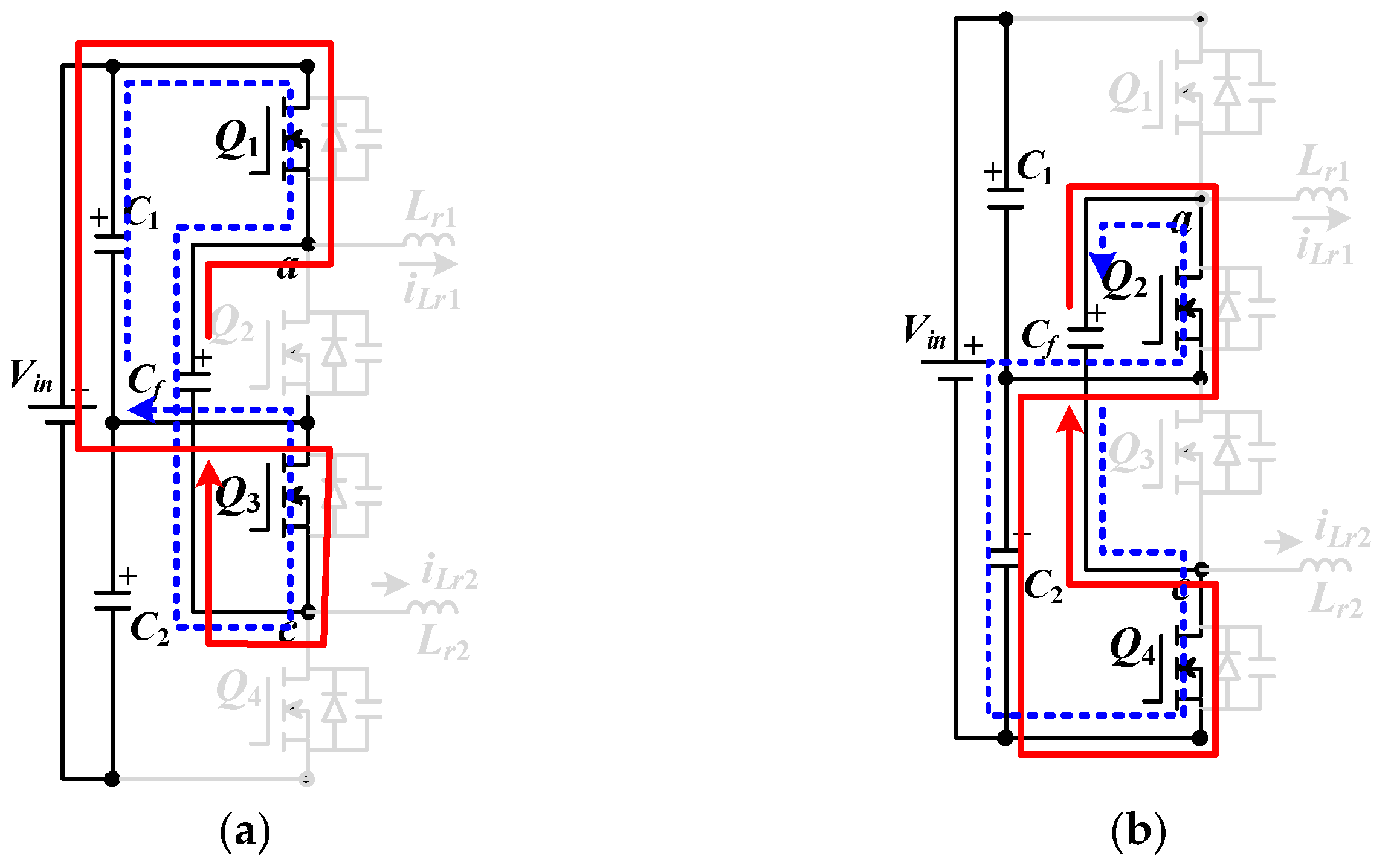
If active devices
Q1 and
Q3 conduct as shown in
Figure 6a, it obtains
vCf =
VC1. If
VC1 is greater (or less) than
VC2, then
C1 will charge (or discharge)
Cf via active devices
Q1 and
Q3. In a similar way,
vCf is equal to
VC2 if active devices
Q2 and
Q4 conduct as shown in
Figure 6b. If
VC1 is greater (or less) then
VC2,
Cf will charge (or discharge)
C2 via active devices
Q2 and
Q4. Therefore,
VC1 and
VC2 are controlled to be balanced at
Vin/2. Fundamental frequency analysis is selected to analyze the transfer function of the studied circuit. The primary inductor voltages
vLm1 =
vLm2 =
nVo/2. According to fundamental harmonic frequency analysis, the equivalent ac resistance is calculated in (7).
Based on the voltage divider of the resonant tank by
Cr1,
Lr1,
Lm1, and
Rac1, the voltage gain of the resonant circuit is calculated in (8).
where
m = Lm/
Lr and
.
The electrical specifications of the proposed circuit in a laboratory prototype are:
Vin = 750 V~800 V,
Vo = 48 V,
Io,max = 21 A, and series resonant frequency
fr = 100 kHz. The unity DC gain of resonant circuit is designed at
Vin = 800 V. The turn-ratio of
T is expressed in (9).
The magnetic core TDK EER-42 (TDK Corporation, Tokyo, Japan) with
Ae = 1.94 cm
2 is selected for transformer with
np = 25 turns and
ns = 3 turns. Then the maximum DC voltage gain at
Vin = 750 V is obtained in (10).
From (7),
Rac under full load is derived in (11).
The selected inductor ratio
m = Lm/
Lr = 10 and quality factor
Q = 0.3
. From the given
Q = 0.3 at full load and
fr = 100 kHz, the series resonant inductors and resonant capacitors are obtained in (12) and (13).
The magnetizing inductances
Lm1 and
Lm2 are obtained in (14).
The current and voltage ratings of
Cr1 and
Cr2 are obtained in (15) and (16).
The average current and voltage ratings of fast recovery diodes are expressed in (17) and (18).
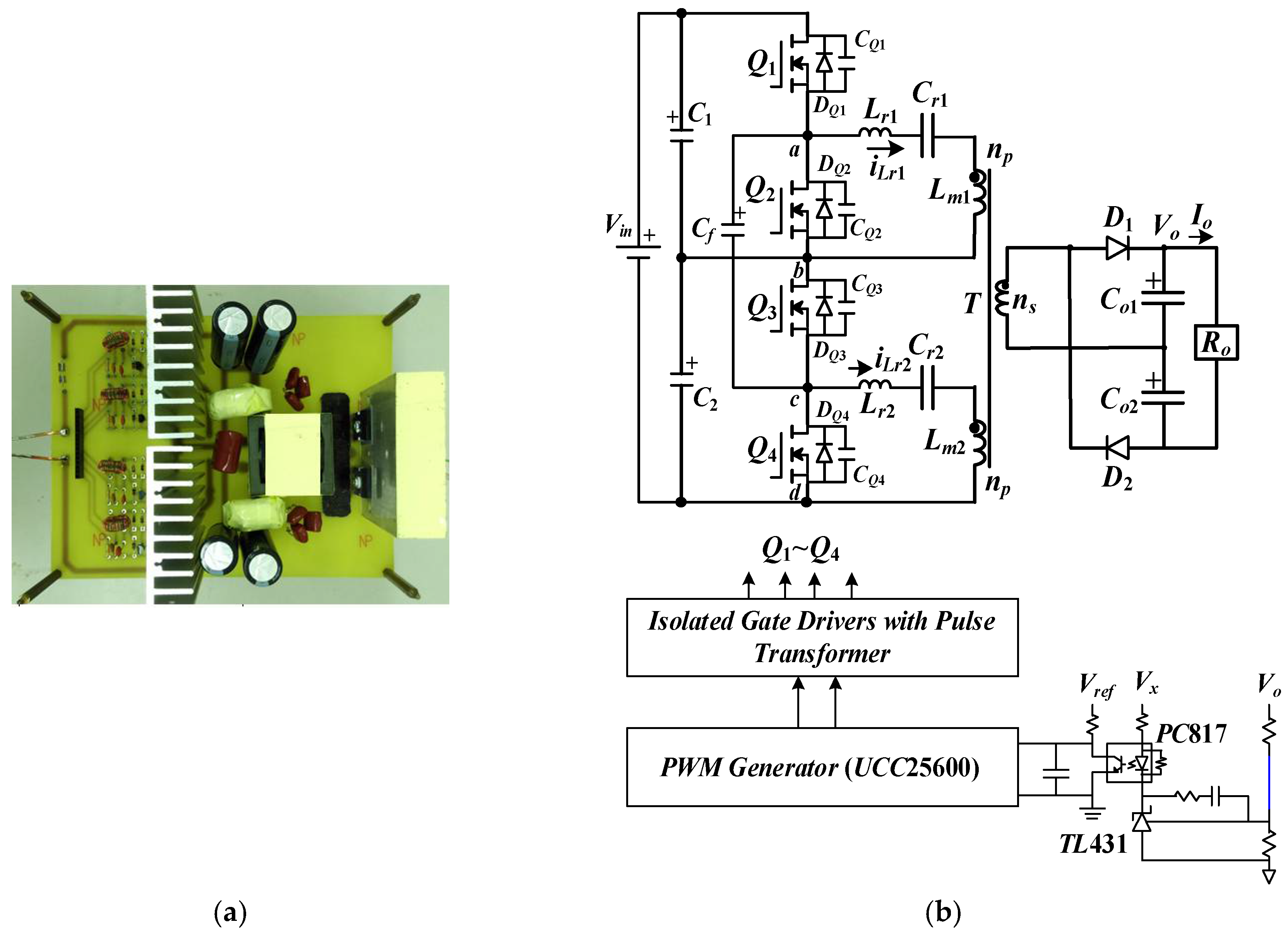
Diodes MBR40200PT are selected for D1 and D2 in the studied converter. The voltage rating of Q1~Q4 equals Vin/2 = 400 V. MOSFETs G20N50C (Vishay Dale Electronics Inc., Pennsylvania, USA) with 500 V voltage stress instead of 1200 V IGBT are used for Q1~Q4. The other capacitors C1 = C2 = 220 μF, Cf = 2.2 μF, and Co1 = Co2 = 2200 μF. A type 2 voltage controller with a shunt voltage regulator based on the TL431 and a photocoupler based on PC817 are used to achieve output voltage control. The frequency control IC with Texas Instruments UCC25600 is selected to control Q1~Q4.
A 1 kW circuit was built and the test results are demonstrated to show the performance of the studied converter. The circuit components of the proposed circuit are obtained from previous section.
Figure 7a gives the photograph of the proposed prototype and
Figure 7b gives the block diagram of the experimental circuit model. The test waveforms shown in
Figure 8,
Figure 9,
Figure 10,
Figure 11,
Figure 12 and
Figure 13 of the converter is supplying 1 kW of output power under
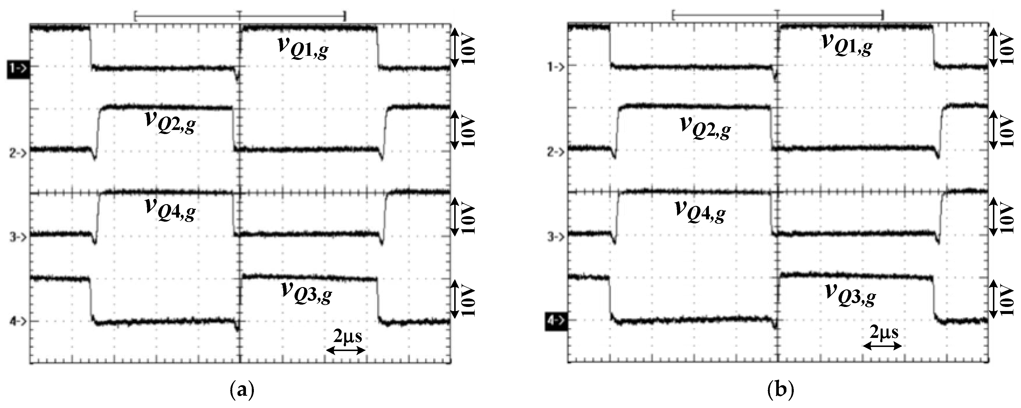
Vin = 750 V. The PWM signals of
Q1~
Q4 of 50% load and 100% load are shown in
Figure 8. The switching frequency at 100% load is less than the frequency at 50% load.
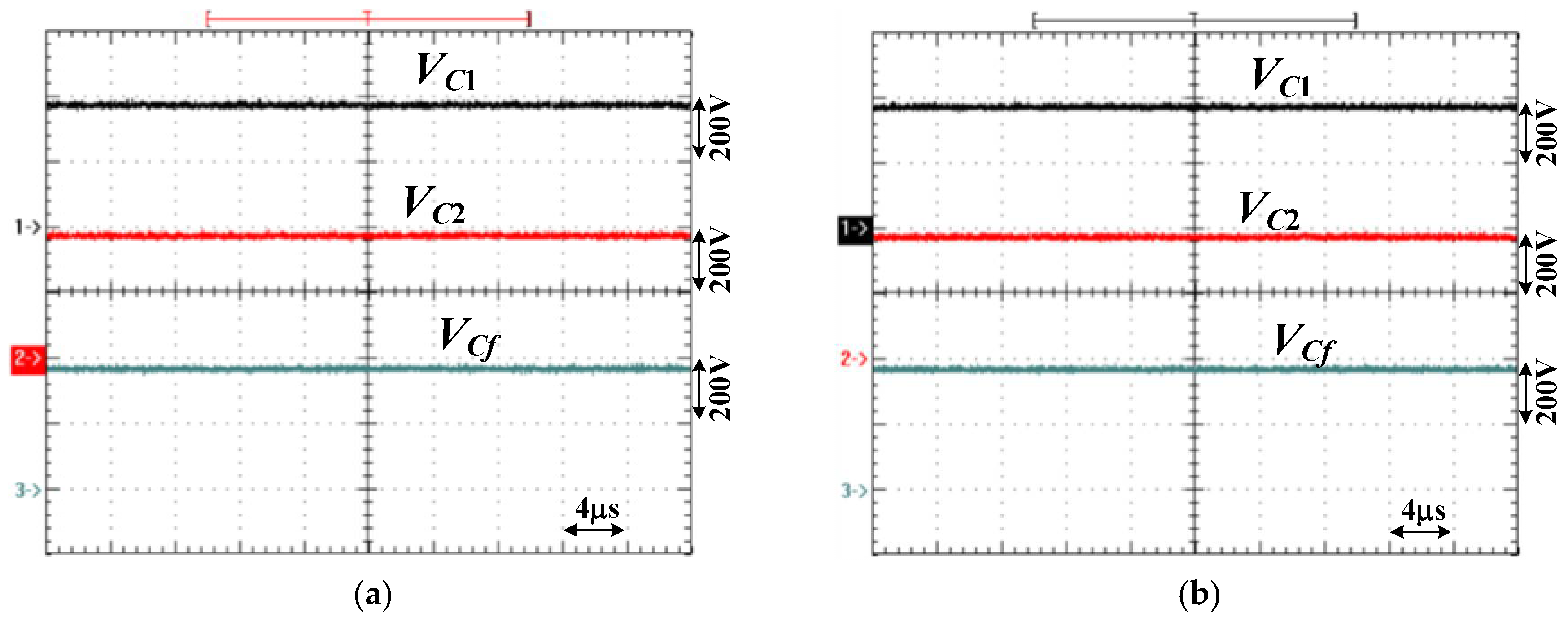
Figure 9 demonstrates the measured waveforms of
VC1,
VC2, and
VCf at 50% load and 100% load. The test experimental waveforms of
VC1,
VC2, and
VCf are balanced.
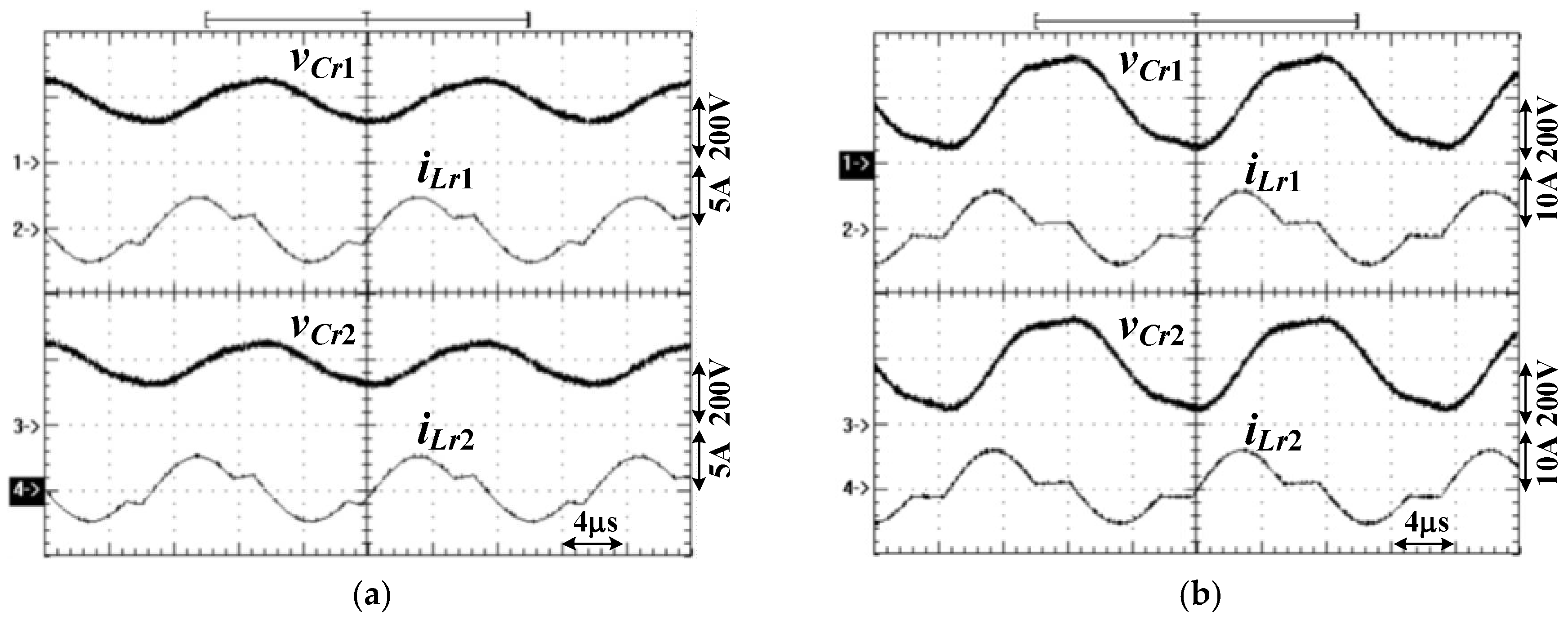
Figure 10 gives the test waveforms of
vCr1,
vCr2,
iLr1, and
iLr2 at 50% and 100% loads. The test results show that
vCr1 and
vCr2 are balanced and
iLr1 and
iLr2 are balanced.
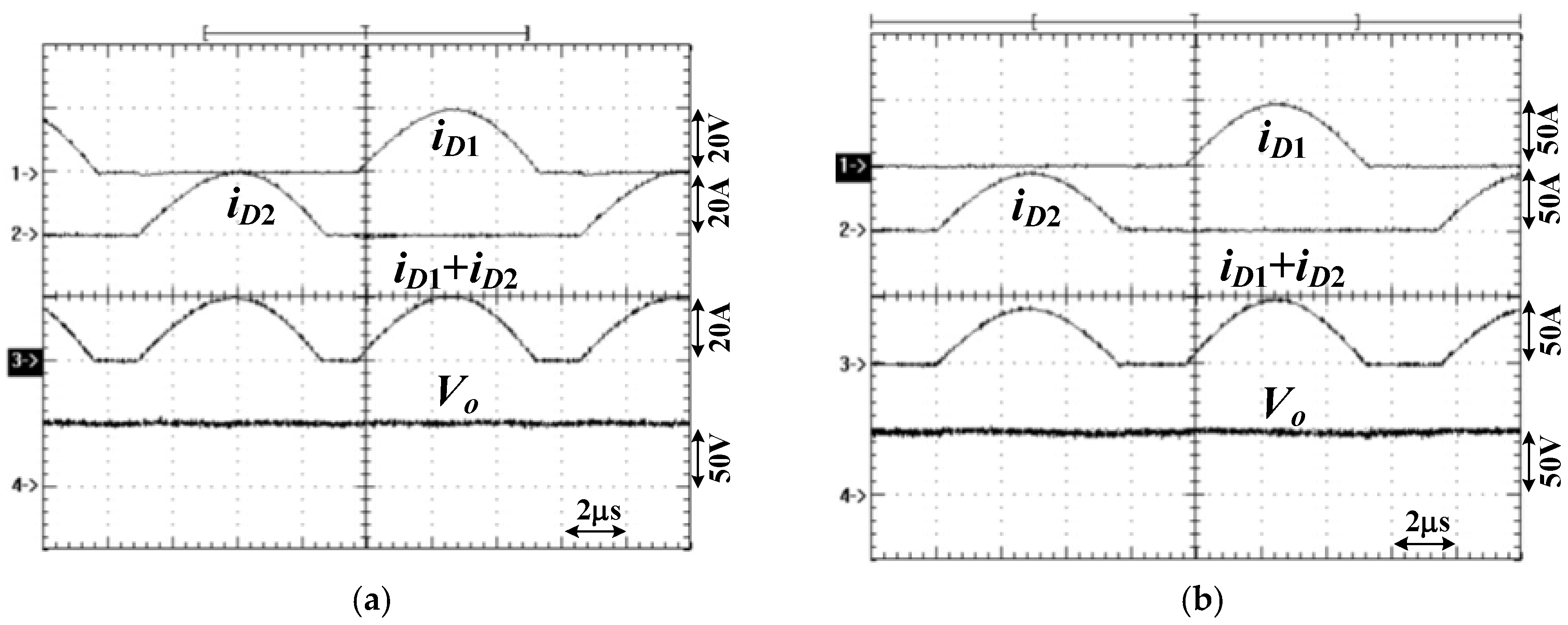
Figure 11 demonstrates the measured
iD1,
iD2,
iD1 +
iD2 and
Vo at 50% and 100% loads. It is observed that the zero-current turn-off of
D1 and
D2 are realized.
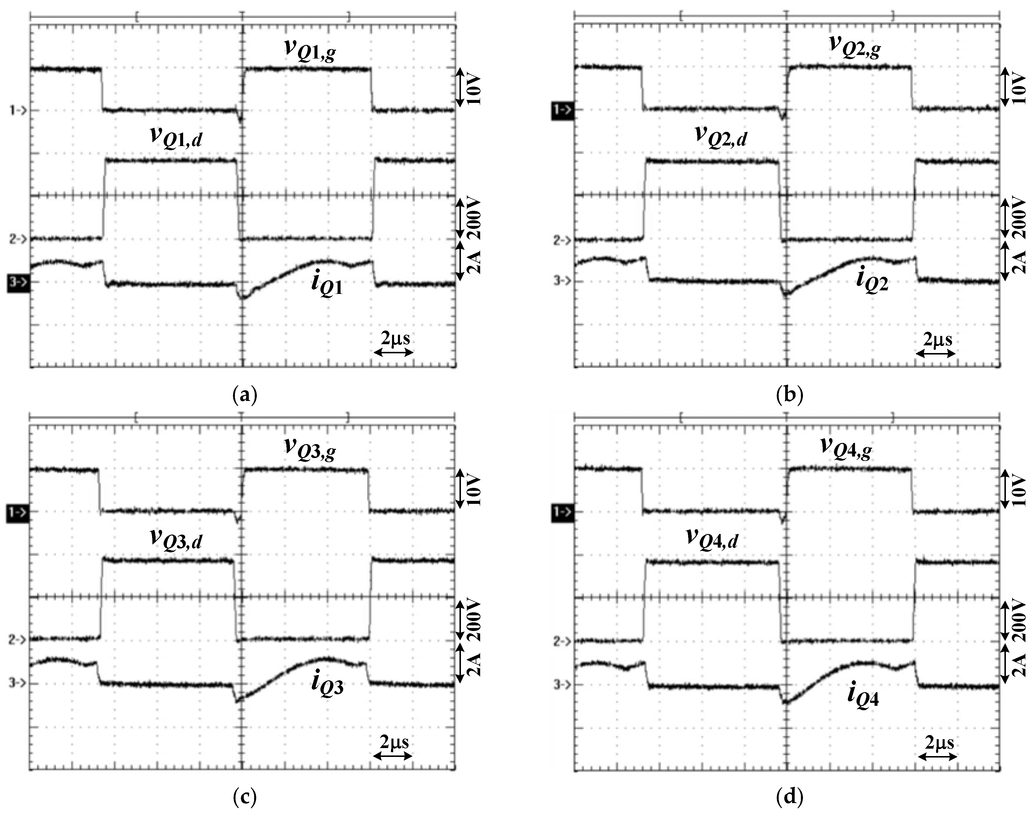
Figure 12 demonstrates the measured voltage and current of
Q1~
Q4 at 20% load. It can observe that
CQ is discharged to zero voltage before switch
Q is active. It can also observe that the voltage stress of each active devices is equal to
Vin/2 = 375 V instead of
Vin = 750 V. Since power devices with low voltage stress are used in the studied converter, the conduction losses due to turn-on resistance of MOSFETs are reduced. Therefore, the power losses on power devices are improved.
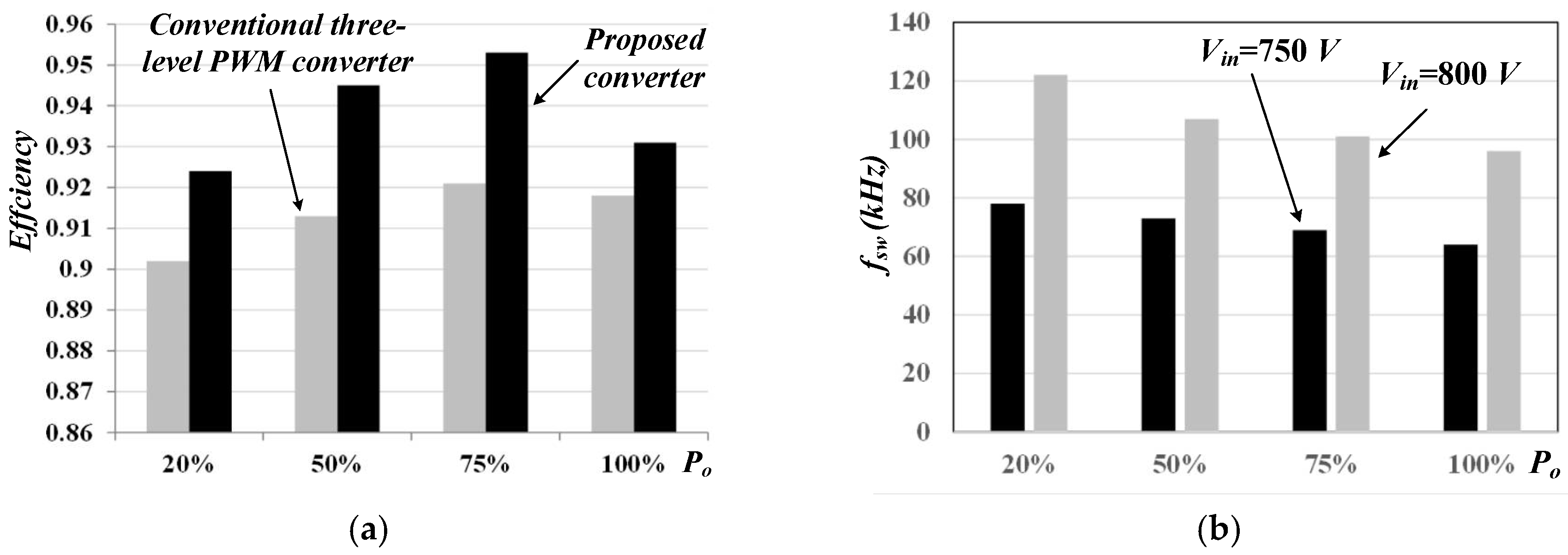
Figure 13a the measured circuit efficiencies of the proposed converter and the conventional three-level phase-shift PWM converter with the same power devices, capacitors, and core size as the proposed converter. This three-level PWM converter have been built in the laboratory for many years to study high input voltage applications. The circuit efficiencies of the proposed converter from 92.3% (at 20% load) to 95.4% (at 75% load) under 750 V input. The measured circuit efficiencies of the conventional three-level PWM converter are from 90% (at 20% load) to 92% (at 75% load). It is clear that the proposed converter has better circuit efficiency. The main reasons of the low circuit efficiency of the conventional three-level PWM converter are high duty loss on heavy load (75% load and 100% load) and high switching frequency at light load (20% load). However, the switching loss on the proposed converter from low load to full load can be removed due to resonant behavior.
Figure 13b gives the measured circuit efficiencies and the frequency range is from 62 kHz to 78 kHz at 750 V input and from 95 kHz to 123 kHz at 800 V input case.


