A Thermoelectric Performance Study of Layered Bi2TeI Weak Topological Insulator Materials


State Key Laboratory of Advanced Technology for Materials Synthesis and Processing, Wuhan University of Technology, Wuhan 430070, China
*
Authors to whom correspondence should be addressed.
Energies 2018, 11(4), 891; https://doi.org/10.3390/en11040891
Submission received: 24 February 2018
/
Revised: 2 April 2018
/
Accepted: 4 April 2018
/
Published: 11 April 2018
(This article belongs to the Section I: Energy Fundamentals and Conversion)
Abstract
:Topological insulators have been considered as promising thermoelectric materials because of their high electrical transport properties and low thermal conductivity. In this work, the crystal structure, chemical composition, and thermoelectric transport properties of a weak topological insulator, Bi2TeI, were studied. Bi2TeI possesses the lowest lattice thermal conductivity compared with the analogously layered compounds Bi2Te3 and BiTeI. Cu and Zn were used as dopants with the aim of optimizing the thermoelectric performance. It was found that doping Bi2TeI with Cu led to decreased carrier concentration and power factor while doping with Zn resulted in increased carrier concentration and improved power factor. Accompanied with reduced lattice thermal conductivity, Zn-doped samples showed a largely improved dimensionless figure of merit, ZT. The largest ZT was 0.077 for Zn0.01Bi2TeI, increased by 70% as compared with the undoped Bi2TeI.
1. Introduction
Thermoelectric (TE) technology can realize direct energy conversion between heat and electricity, having played an important role in the field of waste heat recovering, power generation, and efficient cooling [1]. The performance of a TE material is characterized by the dimensionless figure of merit ZT = α2σT/κ, where α, σ, and T are the Seebeck coefficient, electrical conductivity, and absolute temperature. κ is the thermal conductivity, which is comprised of electronic (κE) and lattice (κL) parts. High-performance TE materials should have high power factor (α2σ) and poor thermal conduction. However, the optimization of TE performance is challenging because these transport properties are strongly interdependent, and it is necessary to synergistically regulate the electrical and thermal transport properties [2,3]. In the past decade, electronic band engineering and phonon engineering approaches have been developed for the improvement of TE properties [4,5,6]. Recently, magnetic nanoparticles embedded in TE materials were reported as a new strategy to optimize the electron and phonon transport [7,8]. It is thus of great interest to explore new materials in which unconventional effects would be beneficial to the TE performance.
As a kind of novel condensed matter, topological insulators (TIs) exhibit gapped states in bulk and nontrivial metallic states on the surface [9,10]. It was suggested that the unique electron transport behavior of the surface states might provide new insights into the TE community [11,12,13,14]. Theoretical calculations have shown that the TE performance of strong TIs such as Bi2Te3 and Bi2Se3 can be enhanced by the surface state hybridization with bulk states [13], or by the largely varied electron scattering rates spanning from the surface states to the bulk states [14]. These studies have provided more opportunities to explore potential TE candidates among the TI systems. As many researchers have focused on the TE performance of the strong TIs [11,12,13,14], the weak TIs, which are distinguished from the strong ones by an even number of Dirac cones on the surface, are less studied as TE materials. Structurally, some weak TIs can be regarded as an alternate stack of quantum spin Hall (QSH) layers and normal insulator (NI) layers [10,15]. The superlattice-like stacked structure should have lower intrinsic lattice thermal conductivity [16,17]. Experimental work has showed that the weak TI Bi14Rh3I9 manifested extremely low thermal conductivity (as low as ~0.3 W m−1 K−1) benefitting from low sound velocity, low Debye temperature, and large lattice anharmonicity [18]. Meanwhile, the first-principles calculations also predicted that low thermal conductivity could be found in another weak TI Bi2TeI due to the similar stacking structure and lattice dynamics [18].
In this work, the weak TI Bi2TeI samples were synthesized using a combination of melting, annealing, and spark plasma sintering (SPS) techniques. The microstructure and TE transport properties of Bi2TeI were studied. The TE properties of Bi2TeI were compared with two other important layered compounds, Bi2Te3 and BiTeI, since Bi2Te3 represents one of the most important TE candidates and is meanwhile a strong TI [13,14], while BiTeI has the same structure as the NI layers of Bi2TeI (Figure 1a) [19,20]. It was found that Bi2TeI possessed the lowest lattice thermal conductivity. Cu and Zn were used as dopants to further improve the TE performance of Bi2TeI. It was revealed that doping Bi2TeI with Zn could improve the TE properties with enhanced electrical conductivity and Seebeck coefficient and depressed thermal conductivity.
2. Experimental
A combination of melting, annealing, and SPS techniques were used to prepare Bi2Te3, BiTeI, and undoped and doped Bi2TeI samples. Highly pure Bi (99.999%, powder), Te (99.999%, powder), and BiI3 (99.99%, powder) were used as starting materials. The mixtures of these materials were weighted according to the compositions and sealed into silica tubes under vacuum. The tubes were transferred into a programmable furnace for heat treatment. For the synthesis of undoped and doped Bi2TeI samples, the tubes were heated to 723 K and held for 8 h followed by an annealing treatment at 403 K for 48 h. The annealed products were ground into fine powders then sintered to pellets by SPS method under vacuum. The sintering temperature was 653 K and the applied pressure was 40 MPa. The synthesis process of Bi2Te3 and BiTeI followed the same procedures. For BiTeI, the melting and annealing treatments were carried out at 893 K for 8 h and at 403 K for 48 h, respectively. The SPS conditions were sintering temperature 653 K and a pressure of 40 MPa. For Bi2Te3, the melting and annealing were carried out at 893 K for 8 h and at 723 K for 48 h, respectively. The SPS conditions were sintering temperature 723 K and a pressure of 40 MPa. Since iodide is volatile, excessive iodide (1 at%) was added in the starting materials to compensate the iodide loss during the annealing and sintering processes of Bi2TeI and BiTeI.
Phase constituents were determined by X-ray diffraction (XRD, PANalytical X’Pert PRO, PANalytical, Almelo, The Netherlands) using Cu Kα radiation. The microstructure and chemical compositions were analyzed by an electron probe micro-analyzer (EPMA, JXA-8230, JEOL, Tokyo, Japan). Selected area electron diffraction (SAED) and elemental mapping of Bi2TeI were performed with transmission electron microscopy (TEM, Talos F200S, Thermo Fisher Scientific, Waltham, MA, USA) equipped with energy dispersion X-ray spectroscopy (EDX). Scanning transmission electron microscopy–energy dispersion X-ray spectroscopy (STEM-EDX) mode was used to capture the elemental distribution in the nanometre scale. The TEM sample for SAED and STEM-EDX analysis was made by a focused ion beam (FIB, Helios NanoLab G3 UC, Thermo Fisher Scientific). σ and α were measured with the standard four-probe method (ZEM-3, ULVAC Technologies, Inc., Kanagawa, Japan) in a He atmosphere. Hall effect measurements were performed on a commercial testing system (Thermoelectric and magnetic performance of multilayer film materials, NYMS-1, Shanghai, China) [7]. The measurements were performed in a He atmosphere with a maximum applied magnetic field of 1.5 T. κ was calculated using the equation κ = Cpλρ0, where Cp is the specific heat capacity, ρ0 is the bulk density, and λ is the thermal diffusion coefficient. λ was measured by a laser flash technique (Netzsch LFA 457, Selb, Germany) in a flowing Ar atmosphere. ρ0 was measured by the Archimedes method. Uncertainties for σ and κ were ±5–7%, and for α was ±5%. Since these layered compounds sintered by the SPS technique exhibited strong c-axis preferred orientation along the direction of pressure, the TE transport properties along the in-plane (perpendicular to the direction of pressure) and cross-plane (parallel to the direction of pressure) directions were separately measured.
3. Results and Discussion
3.1. Synthesis and TE Properties of Bi2TeI
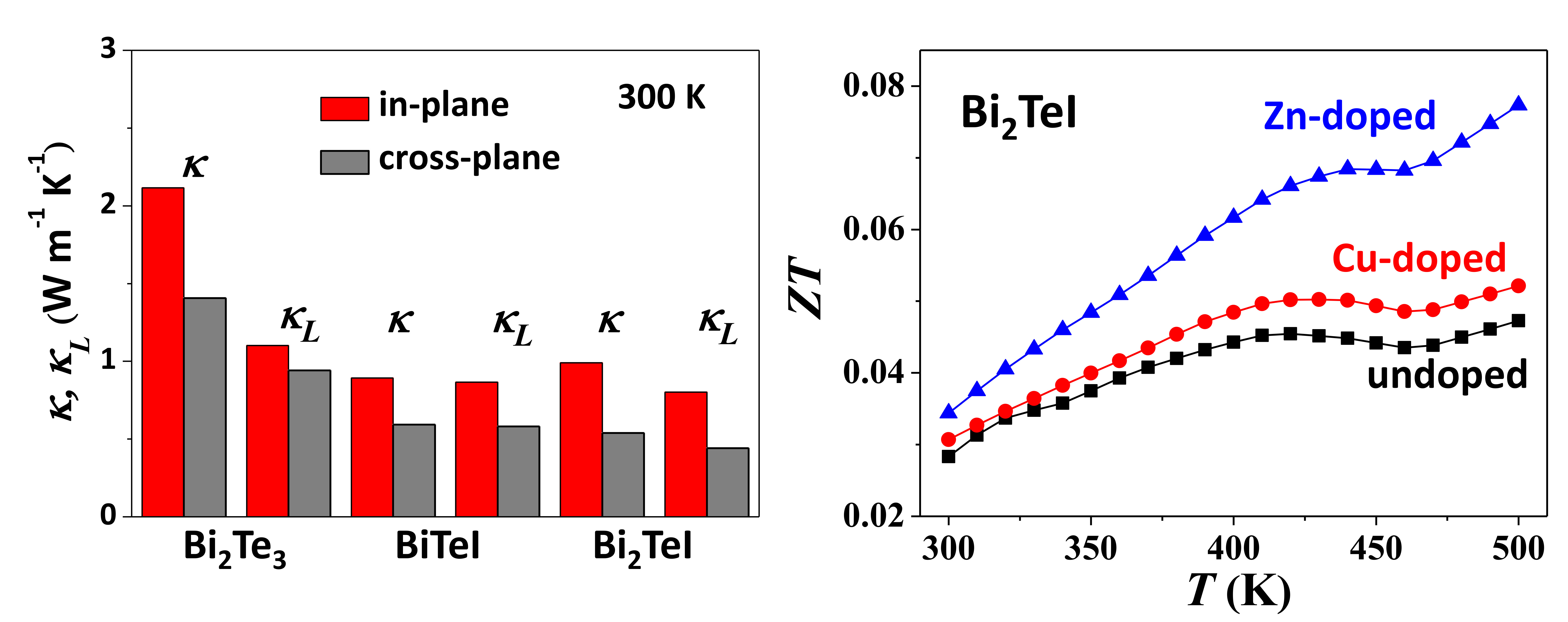
As shown in Figure 1a, Bi2TeI is crystallized in a monoclinic lattice (space group C2/m) [19]. Resembling the weak TI Bi14Rh3I9, Bi2TeI has a layered structure stacked by bismuth QSH bilayers [Bi]2 and BiTeI NI bilayers [BiTeI]2. The formation mechanism of topological insulator states could be connected with the strong interaction between QSH and NI layers [20] and the crystal mirror symmetry [21].
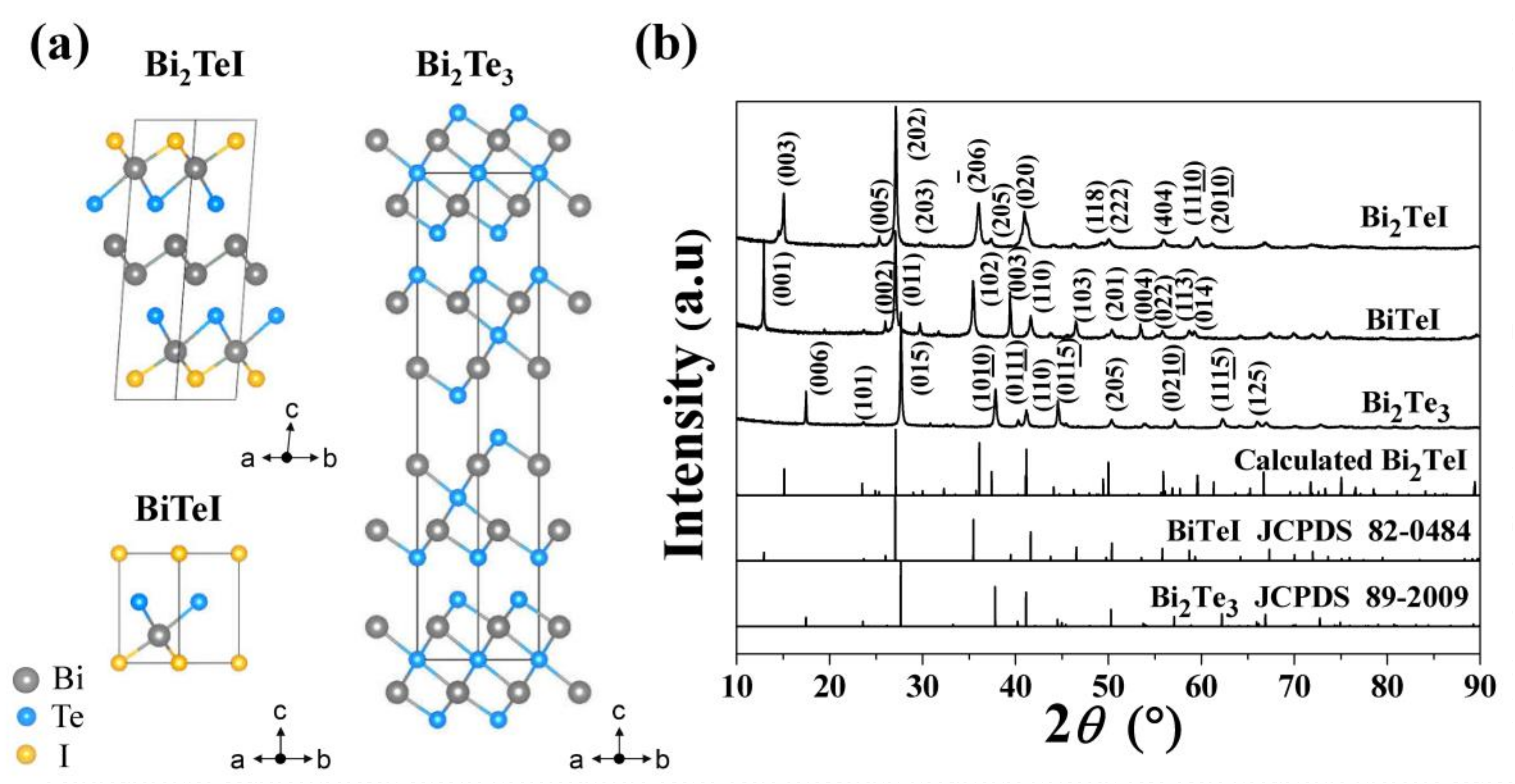
Differently to Bi2Te3 and BiTeI, experimental study performed on Bi2TeI was rare since the preparation of Bi2TeI was a challenge [22,23,24]. It has been reported that phase-pure Bi2TeI could not be obtained by long-term annealing, gas phase reaction, or slow cooling [19,22,23,24]. As guided with the solid-state equilibria of Bi-Te-I systems [25,26,27], polycrystalline Bi2TeI bulk samples were synthesized using a combination of melting, annealing, and SPS techniques in this work. This combined approach has been widely used for preparing varioustable TE materials [2,7]. Figure 1b shows the powder XRD patterns of Bi2Te3, BiTeI, and Bi2TeI. All the diffraction peaks can be indexed to the standard files of the Joint Committee on Powder Diffraction Standards (JCPDS) 89-2009 of Bi2Te3 and the JCPDS 82-0484 of BiTeI, respectively. The XRD pattern of Bi2TeI was calculated with the reported monoclinic structure [16]. All the diffraction peaks can be indexed to the calculated pattern, indicating that the synthesized Bi2TeI was single-phase. Figure 2a,b shows the SAED patterns taken on Bi2TeI sample. The SAED patterns of Bi2TeI can be indexed as [103] and [010] zone axis of the monoclinic crystal structure. The layered structure can be reflected from the SAED pattern along the [010] zone axis, which shows good agreement between the experiment and simulation results. Some diffraction points that were not observed indicated the existence of intrinsic defects in the sample. Figure 2d–f shows the elemental mapping of Bi, Te, and I on Bi2TeI FIB sample. It can be seen that the elements were uniformly distributed in the nanometre scale, indicating the good homogeneity of Bi2TeI samples.
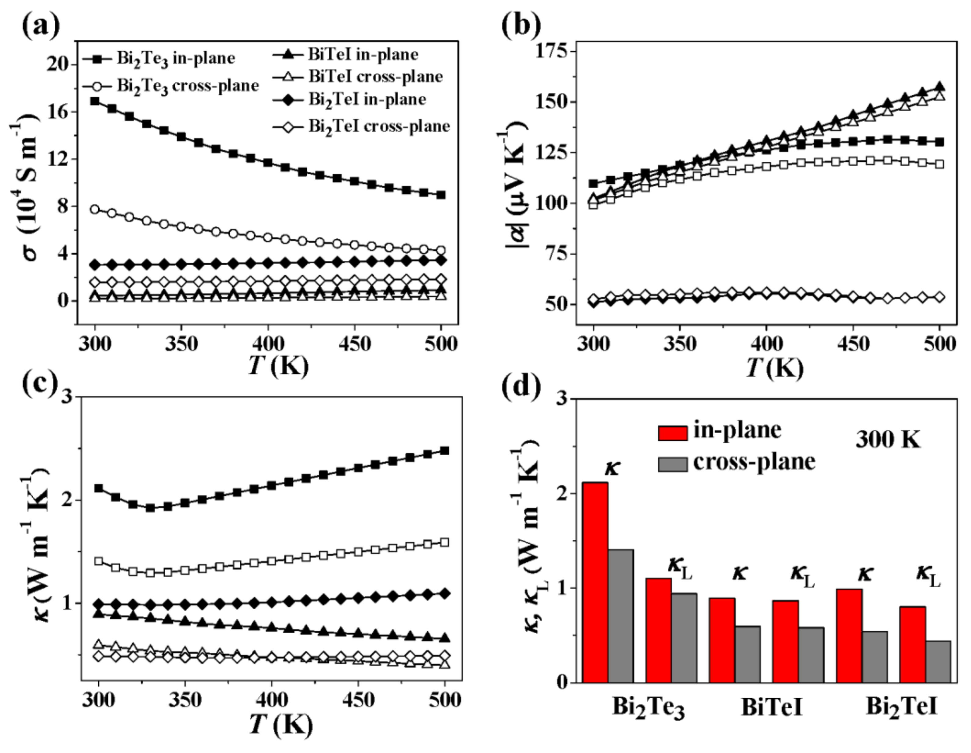
Figure 3 shows the temperature dependence of transport properties of Bi2Te3, BiTeI, and Bi2TeI, including electrical conductivity, absolute Seebeck coefficient, and thermal conductivities measured along the in-plane and cross-plane directions. The charge transport properties at 300 K including carrier concentration and Hall mobility along the two directions are listed in Table 1. Along the two mutually perpendicular directions, the anisotropy in σ was large for Bi2Te3 and BiTeI but in α was small. The anisotropy in layered compounds is determined by the highly anisotropic mobility. σ of Bi2Te3 decreased with the increase in temperature, indicating a heavily doped semiconducting transport behavior. BiTeI and Bi2TeI had σ increased with the increase in temperature, showing a semiconducting transport behavior. Bi2Te3 and BiTeI were n-type while Bi2TeI was p-type. The absolute α of BiTeI was around 100 μV K−1 at 300 K and increased with the increase temperature from 300 to 500 K, which is consistent with the reported work [28]. Bi2TeI had lower α values as compared with BiTeI, which might be related to the higher carrier concentration and much smaller band gap of Bi2TeI (0.1 eV for Bi2TeI [20] and 0.38 eV for BiTeI [29]).
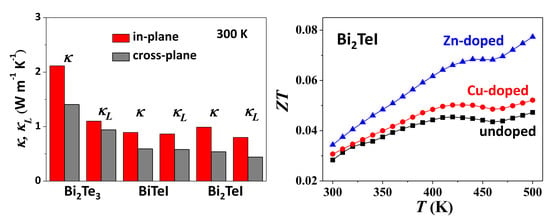
The comparison of thermal conductivity and lattice thermal conductivity of Bi2Te3, BiTeI, and Bi2TeI, along the in-plane and cross-plane directions, is shown in Figure 3c,d. κL was obtained by subtracting κE from κ. κE was calculated by Wiedemann-Franz law κE = L0Tσ, where the Lorenz number L0 had a numerical value of 2.0 × 10⁻⁸ V2 K−2, by considering their high carrier concentration. Compared with binary Bi2Te3, ternary BiTeI and Bi2TeI exhibited much lower κ and relatively weak temperature dependence of κ. At 300 K, κL of Bi2TeI was about 0.44 W m−1 K−1 along the cross-plane direction, which was the lowest as compared with those of Bi2Te3 and BiTeI. The measured κL of Bi2TeI was higher than those predicted by the first-principles calculations [18], which might be attributed to the fact that (1) the sound velocity and Debye temperature were overestimated in the calculations and (2) the contribution of bipolar thermal conductivity as caused by the small band gap was neglected in theoretical calculations.
3.2. TE Properties Optimization of Doped Bi2TeI
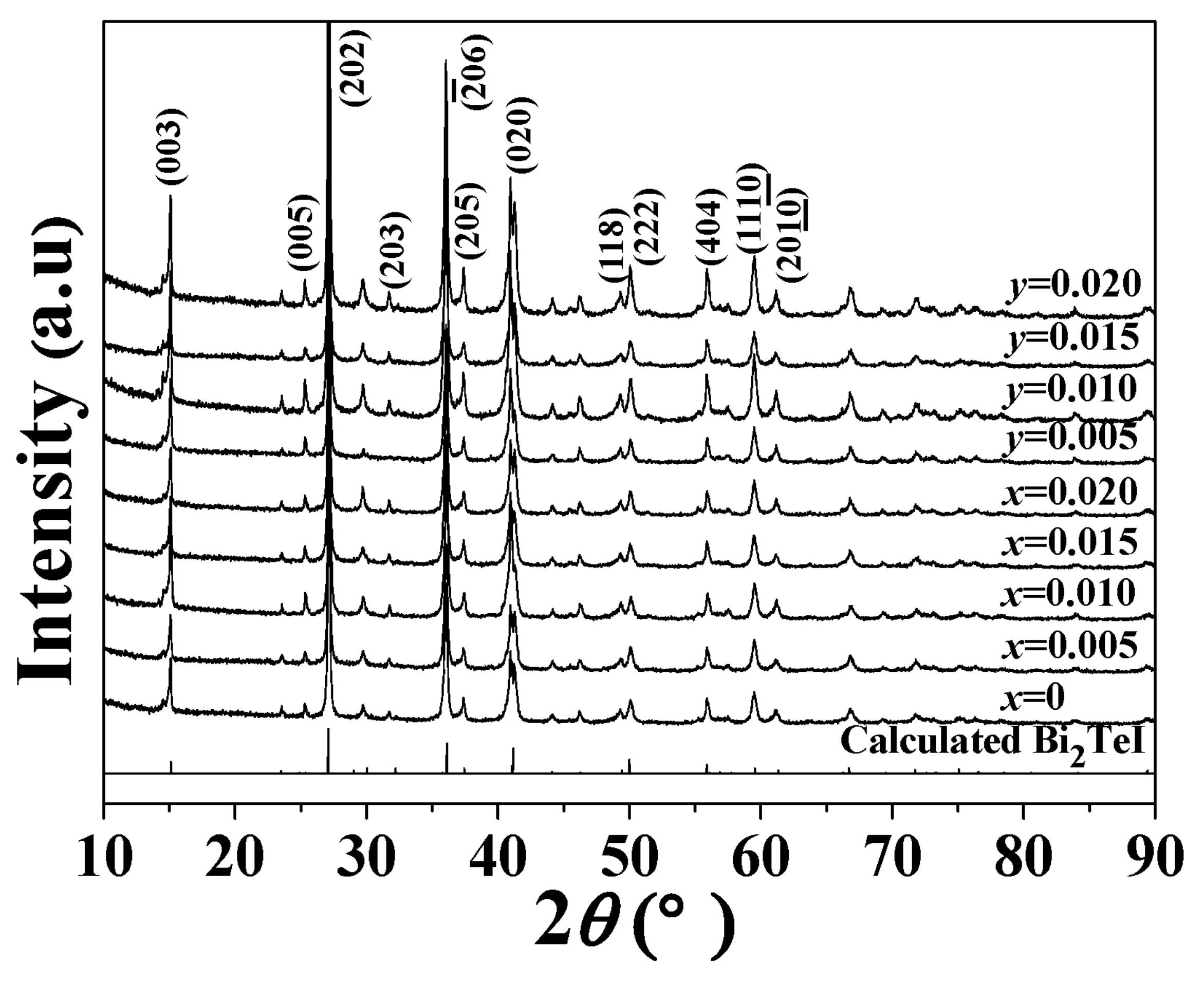
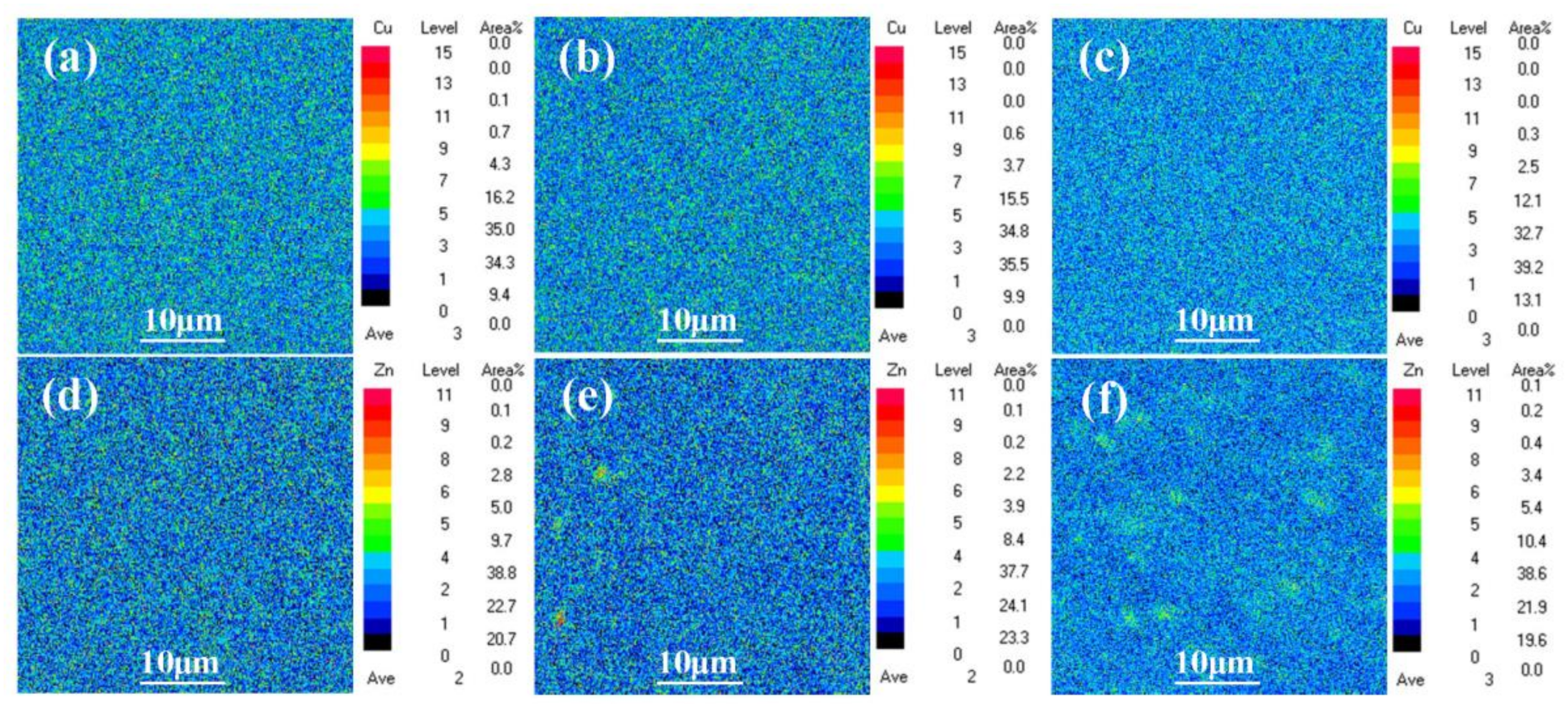
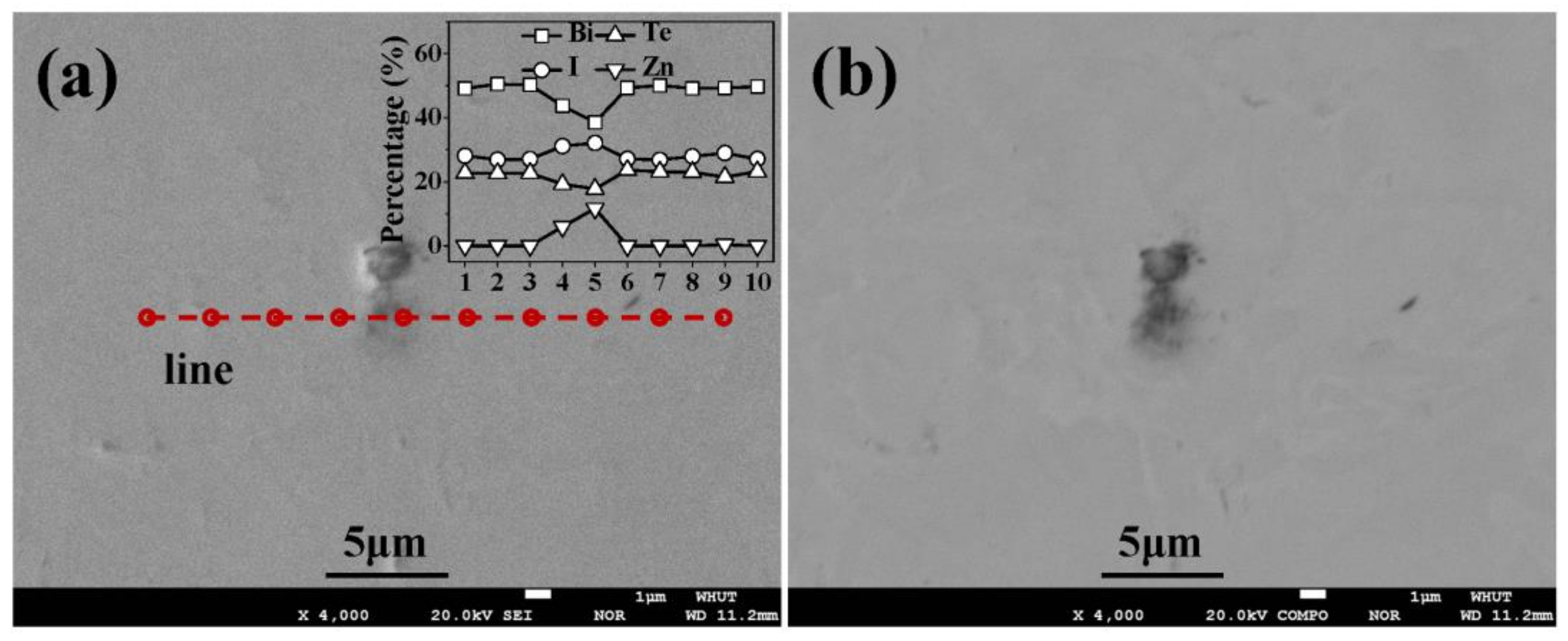
Since Bi2TeI possesses very low lattice thermal conductivity, it is expected to optimize the electrical properties and thus the overall TE performance. A corporation of Cu has been proven as an effective way to improve the TE performance of Bi2Te3 and BiTeI [28,30,31,32]. Here, Cu was used as a dopant to optimize the TE performance of Bi2TeI. Meanwhile, Zn was selected as another dopant because Zn has larger electronegativity. Cu-doped and Zn-doped Bi2TeI samples with nominal compositions CuxBi2TeI and ZnyBi2TeI were synthesized. Figure 4 shows the powder XRD patterns of Cu-doped and Zn-doped Bi2TeI. It can be seen that all the diffraction peaks can be indexed to the calculated diffraction patterns of Bi2TeI, suggesting that Cu and Zn dopants were incorporated into the lattice of Bi2TeI. Broadened diffraction peaks can be found for the (003), (205), and (020) planes. It is possible that the high concentration of dopants could bring about large lattice distortion. Figure 5 shows the elemental mapping of Cu on CuxBi2TeI and Zn on ZnyBi2TeI samples measured by EPMA. For CuxBi2TeI, the distribution of Cu was uniform with increasing the content of dopant. A slight Zn richness can be found from y = 1.5% and 2% samples. Figure 6 shows the chemical composition of a large Zn-rich area on Zn0.015Bi2TeI sample determined by EPMA. Further analysis indicated that the Zn-rich area was composed of Bi2TeI and ZnI2. Combined with the distribution of Zn for y = 1.5% and 2% samples as shown in Figure 5e,f, the secondary phase ZnI2 should be precipitated on the grain boundaries of the matrix, which will impact the electrical and thermal properties. These results suggest that Cu and Zn were incorporated into the lattice of Bi2TeI and a high concentration of Zn led to the formation of ZnI2 impurity phase.
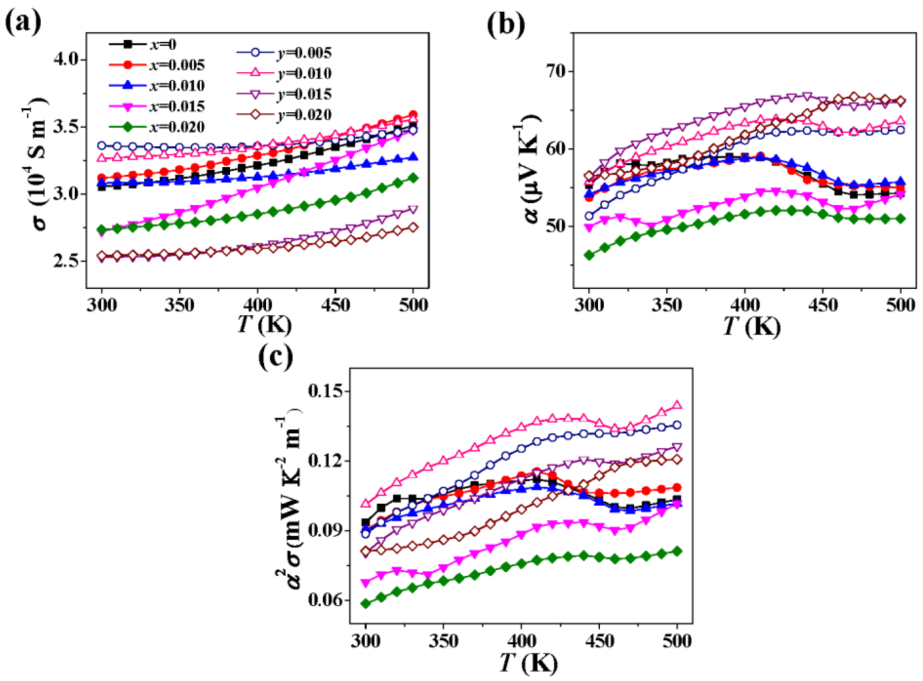
Figure 7 shows the temperature dependence of in-plane electrical conductivity, Seebeck coefficient, and power factor of Cu- and Zn-doped Bi2TeI. The in-plane charge transport properties of Cu-doped CuxBi2TeI and Zn-doped ZnyBi2TeI at 300 K are listed in Table 2. σ of the doped samples was increased slowly while increasing the temperature, indicating a semiconducting transport behavior. Doping Bi2TeI with 1.5% and 2% Cu led to decreased σ. With increasing the Zn content, σ of ZnyBi2TeI was first increased then largely decreased. The decrease in σ upon doping with large amount of Cu should be attributed to the decreased carrier concentration. After doping with Zn, the carrier concentration was greatly increased, from 8.1 × 1020 cm−3 for the pristine Bi2TeI to 1.48 × 1021 cm−3 for Zn0.01Bi2TeI, and kept almost unchanged after doping with 2% Zn. Therefore, the increase in σ for Zn0.01Bi2TeI was due to the increased carrier concentration, and the decrease in σ for Zn0.015Bi2TeI and Zn0.02Bi2TeI might be related to the formation of nonconductive ZnI2 impurity phase. Since the carrier concentration was reduced after Cu doping, it can be inferred that Cu as an intercalated dopant has entered into the interlayer space of Bi2TeI. The electron donor behavior of the intercalated Cu has been reported in other layered compounds [29,30]. For Zn doped samples, a substitution of Zn2+ on Bi3+ sites might be accounted for the increased carrier concentration of the p-type materials.
The positive α values of CuxBi2TeI and ZnyBi2TeI were indicative of p-type conduction behavior, which was consistent with Hall effect measurements. Doping Cu led to not only decreased σ but also decreased α, which was mainly related to the strengthened bipolar effect as the carrier concentration was decreased. Interestingly, simultaneously increased σ and α were obtained for Zn0.01Bi2TeI sample. It was highly possible that the dopant Zn introduced an additional resonant state near the Fermi level, which was beneficial for enhancing the Seebeck coefficient. However, a further theoretical calculation should be carried out to verify the electronic structure of Zn-doped Bi2TeI.
Due to the decreased σ and α, the α2σ values of the Cu-doped samples decreased with increasing x in the range of 0–2%. This result originated from the strengthened bipolar effect as caused by the lowered carrier concentration. For Zn-doped samples, the α2σ values first increased and then decreased. The highest value reached 0.14 mW m−1 K−2 at 500 K for Zn0.01Bi2TeI sample, which showed an approximately 50% improvement as compared with that of the undoped sample. At high temperatures, all Zn doped samples showed enhanced power factors.
Theoretical predictions have suggested that the gapless surface states on the surface could bring about positive contribution to the Seebeck coefficient [13,14], which needs to adjust the Fermi level into a relatively narrow energy range [12,21]. The undoped Bi2TeI had a high carrier concentration of 8 × 1020 cm−3. By inserting Cu, the carrier concentration of Bi2TeI can be reduced to 4 × 1020 cm−3. However, an increase in Cu content to further lower the carrier concentration failed and finally led to the formation of impurities. Therefore, the TE properties of the undoped and doped Bi2TeI in this work should be contributed from the bulk states of this weak TI.
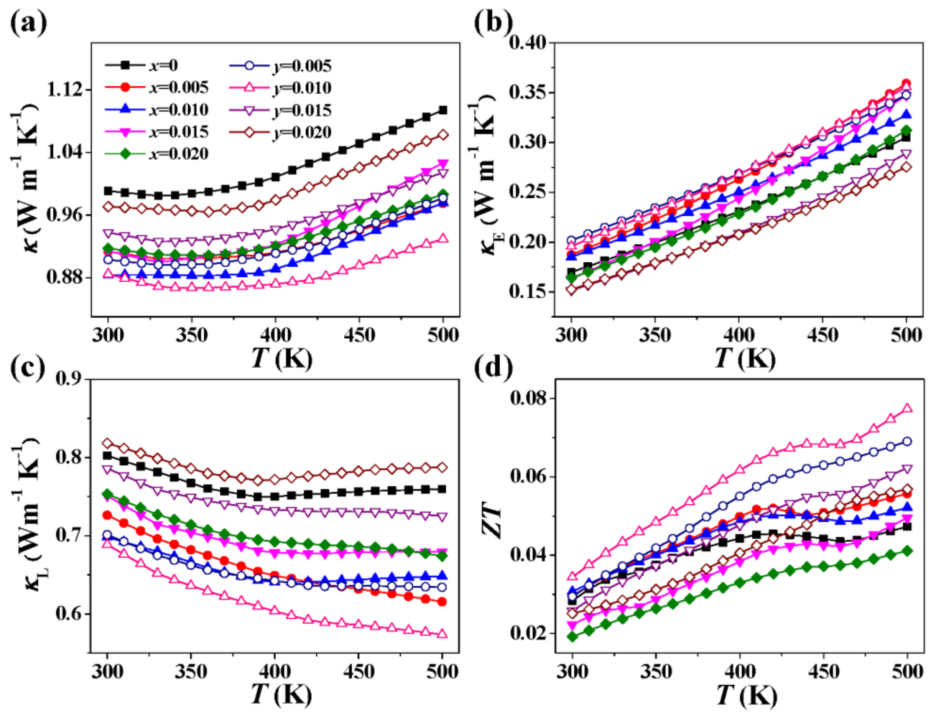
Figure 8 shows the temperature dependence of in-plane thermal conductivity, carrier thermal conductivity, and lattice thermal conductivity of Cu-doped and Zn-doped Bi2TeI. With an increase in temperature from 300 to 500 K, κ first decreased slightly and then increased gradually. The first decrease in κ was related to the phonon–phonon scattering and the increase at higher temperatures should be mainly due to the contribution of κE. The κL values for all the samples decreased with the increase in temperature, reflecting strong phonon–phonon scattering in the layered Bi2TeI. With the increase in the doping content of Cu and Zn, the κL values first decreased and then increased. The first decrease in κL values with doping Cu might originate from the point defect scattering and disorder scattering of the intercalated Cu. The increase in κL values after doping more Cu should be related to the enhanced interlayer coupling between QSH and NI layers in these kinds of layered materials. It was inferred that the intercalation of dopants could lead to increased sound velocity and Debye temperature along the cross-plane directions, which leads to higher κL. The first decrease in κL values after doping with Zn should originate from the improved point defect scattering when the dopant Zn substituted for the Bi sites. The increase in κL values after doping more Zn should be attributed to the presence of ZnI2 impurity. Zn0.01Bi2TeI had the lowest in-plane lattice thermal conductivity with 0.69 W m−1 K−1 at 300 K and 0.58 W m−1 K−1 at 500 K.
Figure 8d displays the ZT values of the doped Bi2TeI in the temperature range of 300–500 K. With the increase in temperature, the ZT values of all the samples increased gradually. With increasing the content of Cu, the ZT values of Cu-doped samples first slightly increased and then decreased. However, ZnyBi2TeI showed increased ZT with increasing y in the range of 0–1%. At high temperatures, all Zn-doped samples showed increased ZT values. The largest ZT reached 0.077 at 500 K for the Zn0.01Bi2TeI sample, increased by 70% as compared with that of the undoped Bi2TeI. The reason behind the enhancement of ZT was twofold: (1) lowered lattice thermal conductivity due to the substitution of Zn on Bi sites and (2) simultaneously improved electrical conductivity and Seebeck coefficient.
4. Conclusions
Single-phase Bi2TeI was prepared by a combination of melt-annealing and SPS techniques. The TE performance of Bi2TeI was compared with Bi2Te3 and BiTeI. It was found that Bi2TeI possessed high electrical conductivity and the lowest lattice thermal conductivity. A performance optimization study was performed by doping Bi2TeI with Cu and Zn. Structural analysis indicated that the dopants Cu and Zn were incorporated into the lattice of Bi2TeI. The doping of Zn could improve the power factor due to the enhanced electrical conductivity and Seebeck coefficient. The maximal power factor reached 0.14 mW m−1 K−2 at 500 K for the Zn0.01Bi2TeI sample. The phonon transport of Bi2TeI was suppressed due to the intercalation of Cu into the interlayer space and the substitution of Zn on Bi sites. The phonon scattering mechanisms included enhanced point defect scattering due to the Zn substitution and disorder scattering as a result of Cu intercalation. The largest ZT was 0.077 for the Zn0.01Bi2TeI sample, increased by 70% as compared with the undoped Bi2TeI. This work demonstrated that doping a proper amount of Zn can optimize the TE performance of Bi2TeI materials.
Acknowledgments
This work was supported by National Natural Science Foundation of China (Nos. 51502228 and 51572210).
Author Contributions
Ping Wei and Wenyu Zhao conceived and designed the experiments; Kaihua Tu, Hongyu Zhou, and Xin Mu performed the experiments; Ping Wei and Wenyu Zhao analyzed the data; Wanting Zhu and Xiaolei Nie contributed analysis tools; Kaihua Tu, Ping Wei, and Wenyu Zhao wrote the paper.
Conflicts of Interest
The authors declare no conflict of interest.
References
- Snyder, G.J.; Toberer, E.S. Complex thermoelectric materials. Nature Mater. 2008, 7, 105–114. [Google Scholar] [CrossRef] [PubMed]
- Zhu, T.J.; Liu, Y.T.; Fu, C.G.; Heremans, J.P.; Snyder, J.G.; Zhao, X.B. Compromise and synergy in high-efficiency thermoelectric materials. Adv. Mater. 2017, 29, 1–26. [Google Scholar] [CrossRef] [PubMed]
- Shi, X.; Chen, L.; Uher, C. Recent advances in high-performance bulk thermoelectric materials. Inter. Mater. Rev. 2016, 61, 379–415. [Google Scholar] [CrossRef]
- Sootsman, J.R.; Chung, D.Y.; Kanatzidis, M.G. New and old concepts in thermoelectric materials. Angew. Chem. Int. Ed. 2009, 48, 8616–8939. [Google Scholar] [CrossRef] [PubMed]
- Yang, J.; Yip, H.-L.; Jen, A.K.-Y. Rational design of advanced thermoelectric materials. Adv. Energy Mater. 2013, 3, 549–565. [Google Scholar] [CrossRef]
- Su, X.L.; Wei, P.; Li, H.; Liu, W.; Yan, Y.G.; Li, P.; Su, C.Q.; Xie, C.J.; Zhao, W.Y.; Zhai, P.C.; et al. Multi-scale microstructural thermoelectric materials: Transport behavior, non-equilibrium preparation, and applications. Adv. Mater. 2017, 29, 1602013. [Google Scholar] [CrossRef] [PubMed]
- Zhao, W.Y.; Liu, Z.Y.; Wei, P.; Zhang, Q.J.; Zhu, W.T.; Tang, X.F.; Yang, J.H.; Liu, Y.; Shi, J.; Chao, Y.M.; et al. Magnetoelectric interaction and transport behaviours in magnetic nanocomposite thermoelectric materials. Nature Nanotechnol. 2017, 12, 55–60. [Google Scholar] [CrossRef] [PubMed]
- Zhao, W.Y.; Liu, Z.Y.; Sun, Z.G.; Zhang, Q.J.; Wei, P.; Mu, X.; Zhou, H.Y.; Li, C.C.; Ma, S.F.; He, D.Q.; et al. Superparamagnetic enhancement of thermoelectric performance. Nature 2017, 549, 247–251. [Google Scholar] [CrossRef] [PubMed]
- Fu, L.; Kane, C.L.; Mele, E.J. Topological insulators in three dimensions. Phys. Rev. Lett. 2007, 98, 106803. [Google Scholar] [CrossRef] [PubMed]
- Hasan, M.Z.; Kane, C.L. Colloquium: Topological Insulators. Rev. Mod. Phys. 2010, 82, 3045–3067. [Google Scholar] [CrossRef]
- Kong, D.; Cui, Y. Opportunities in chemistry and materials science for topological insulators and their nanostructures. Nature Chem. 2011, 3, 845–849. [Google Scholar] [CrossRef] [PubMed]
- Müchler, L.; Casper, F.; Yan, B.; Chadov, S.; Felser, C. Topological insulators and thermoelectric materials. Phys. Status Solidi RRL 2013, 7, 91–100. [Google Scholar] [CrossRef]
- Ghaemi, P.; Mong, R.S.K.; Moore, J.E. In-plane transport and enhanced thermoelectric performance in thin films of the topological insulators Bi2Te3 and Bi2Se3. Phys. Rev. Lett. 2010, 105, 166603. [Google Scholar] [CrossRef] [PubMed]
- Xu, Y.; Gan, Z.; Zhang, S.-C. Enhanced thermoelectric performance and anomalous Seebeck effects in topological insulators. Phys. Rev. Lett. 2014, 112, 226801. [Google Scholar] [CrossRef] [PubMed]
- Rasche, B.; Isaeva, A.; Ruck, M.; Borisenko, S.; Zabolotnyy, V.; Büchner, B.; Koepernik, K.; Ortix, C.; Richter, M.; van den Brink, J. Stacked topological insulator built from bismuth-based graphene sheet analogues. Nature Mater. 2013, 12, 422–425. [Google Scholar] [CrossRef] [PubMed]
- Dresselhaus, M.S.; Chen, G.; Tang, M.Y.; Yang, R.; Lee, H.; Wang, D.; Ren, Z.; Fleurial, J.-P.; Gogna, P. New directions for low-dimensional thermoelectric materials. Adv. Mater. 2007, 19, 1043–1053. [Google Scholar] [CrossRef]
- Venkatasubramanian, R.; Siivola, E.; Colpitts, T.; O’Quinn, B. Thin-film thermoelectric devices with high room-temperature figures of merit. Nature 2001, 413, 597–602. [Google Scholar] [CrossRef] [PubMed]
- Wei, P.; Yang, J.; Guo, L.; Wang, S.Y.; Wu, L.H.; Xu, X.F.; Zhao, W.Y.; Zhang, Q.J.; Zhang, W.Q.; Dresselhaus, M.S.; et al. Minimum thermal conductivity in weak topological insulators with bismuth-based stack structure. Adv. Funct. Mater. 2016, 26, 5360–5367. [Google Scholar] [CrossRef]
- Savilov, S.V.; Khrustalev, V.N.; Kuznetsov, A.N.; Popovkin, B.A.; Antipin, M.Y. New subvalent bismuth telluroiodides incorporating Bi2, layers: The crystal and electronic structure of Bi2TeI. Russ. Chem. Bull. 2005, 54, 87–92. [Google Scholar] [CrossRef]
- Tang, P.; Yan, B.; Cao, W.; Wu, S.; Felser, C.; Duan, W. Weak topological insulators induced by the inter-layer coupling: A first-principles study of stacked Bi2TeI. Phys. Rev. B 2014, 89, 041409(R). [Google Scholar] [CrossRef]
- Rusinov, I.P.; Menshchikova, T.V.; Isaeva, A.; Eremeev, S.V.; Koroteev, Y.M.; Vergniory, M.G.; Echenique, P.M.; Chulkov, E.V. Mirror-symmetry protected non-TRIM surface state in the weak topological insulator Bi2TeI. Sci. Rep. 2016, 6, 20734. [Google Scholar] [CrossRef] [PubMed]
- Moroz, M.V.; Prokhorenko, M.V. Phase equilibria and the thermodynamic properties of saturated solid solutions of BiTeI, Bi2TeI, and Bi4TeI1.25, compounds of the AgI-Bi-Bi2Te3-BiTeI system. Russ. J. Phys. Chem. A 2016, 90, 1301–1305. [Google Scholar] [CrossRef]
- Ryu, G.; Son, K.; Schütz, G. Growth and characterization of large weak topological insulator Bi2TeI single crystal by Bismuth self-flux method. J. Crystal Growth 2016, 440, 26–30. [Google Scholar] [CrossRef]
- Zeugner, A.; Kaiser, M.; Schmidt, P.; Menshchikova, T.V.; Rusinov, I.P.; Markelov, A.V.; van den Broek, W.; Chulkov, E.V.; Doert, T.; Ruck, M.; et al. Modular design with 2D topological-insulator building blocks: Optimized synthesis and crystal growth, crystal and electronic structures of BixTeI (x = 2, 3). Chem. Mater. 2017, 29, 1321–1337. [Google Scholar] [CrossRef]
- Tomokiyo, A.; Okada, T.; Kawano, S. Phase diagram of system (Bi2Te3)-(BiI3) and crystal structure of BiTeI. Jpn. J. Appl. Phys. 1977, 16, 291–298. [Google Scholar] [CrossRef]
- Aliyev, Z.S.; Babanly, M.B. Solid-state equilibria and thermodynamic properties of compounds in the Bi-Te-I system. Inorg. Mater. 2008, 44, 1076–1080. [Google Scholar] [CrossRef]
- Babanly, M.B.; Tedenac, J.; Aliyev, Z.S.; Balitsky, D.V. Phase equilibriums and thermodynamic properties of the system Bi-Te-I. J. Alloys Compd. 2009, 481, 349–353. [Google Scholar] [CrossRef]
- Wu, L.; Yang, J.; Chi, M.; Wang, S.; Wei, P.; Zhang, W.; Chen, L.; Yang, J. Enhanced thermoelectric performance in Cu-intercalated BiTeI by compensation weakening induced mobility improvement. Sci. Rep. 2015, 5, 14319. [Google Scholar] [CrossRef] [PubMed]
- Ishizaka, K.; Bahramy, M.S.; Murakawa, H.; Sakano, M.; Shimojima, T.; Sonobe, T.; Koizumi, K.; Shin, S.; Miyahara, H.; Kimura, A.; et al. Giant Rashba-type spin splitting in bulk BiTeI. Nature Mater. 2011, 10, 521–526. [Google Scholar] [CrossRef] [PubMed]
- Liu, W.S.; Zhang, Q.Y.; Lan, Y.C.; Chen, S.; Yan, X.; Zhang, Q.; Wang, H.; Wang, D.Z.; Chen, G.; Ren, Z.F. Thermoelectric property studies on Cu-doped n-type CuxBi2Te2.7Se0.3 nanocomposites. Adv. Energy Mater. 2011, 1, 577–587. [Google Scholar] [CrossRef]
- Wang, S.Y.; Li, H.; Lu, R.M.; Zheng, G.; Tang, X.F. Metal nanoparticle decorated n-type Bi2Te3-based materials with enhanced thermoelectric performances. Nanotechnology 2013, 24, 285702. [Google Scholar] [CrossRef] [PubMed]
- Cui, J.L.; Mao, L.D.; Yang, W.; Xu, X.B.; Chen, D.Y.; Xiu, W.J. Thermoelectric properties of Cu-doped n-type (Bi2Te3)0.9–(Bi2−xCuxSe3)0.1(x = 0–0.2) alloys. J. Solid State Chem. 2007, 180, 3583–3587. [Google Scholar] [CrossRef]
Figure 1.
(a) Crystal structures of Bi2TeI, BiTeI, and Bi2Te3. (b) Powder XRD patterns of Bi2TeI, BiTeI, and Bi2Te3 synthesized by a combination of melting, annealing, and spark plasma sintering techniques.
Figure 1.
(a) Crystal structures of Bi2TeI, BiTeI, and Bi2Te3. (b) Powder XRD patterns of Bi2TeI, BiTeI, and Bi2Te3 synthesized by a combination of melting, annealing, and spark plasma sintering techniques.

Figure 2.
Selected area electron diffraction (SAED) patterns of Bi2TeI along the zone axis of (a) [103], (b) [010], and (c) simulated SAED pattern along [010] zone axis. Elemental mapping of (d) Bi, (e) Te, and (f) I of Bi2TeI measured by Scanning transmission electron microscopy–energy dispersion X-ray spectroscopy (STEM-EDX).

Figure 3.
Temperature dependence of (a) electrical conductivity, (b) Seebeck coefficient, (c) thermal conductivity, and (d) comparison of the thermal conductivity and lattice thermal conductivity of Bi2Te3, BiTeI, and Bi2TeI at 300 K.
Figure 3.
Temperature dependence of (a) electrical conductivity, (b) Seebeck coefficient, (c) thermal conductivity, and (d) comparison of the thermal conductivity and lattice thermal conductivity of Bi2Te3, BiTeI, and Bi2TeI at 300 K.

Figure 4.
XRD patterns of Cu-doped CuxBi2TeI and Zn-doped ZnyBi2TeI.

Figure 5.
Elemental mapping of (a–c) Cu on CuxBi2TeI and (d–f) Zn on ZnyBi2TeI samples. (a) x = 1%, (b) x = 1.5%, (c) x = 2%, (d) y = 1%, (e) y = 1.5%, (f) y = 2%.
Figure 5.
Elemental mapping of (a–c) Cu on CuxBi2TeI and (d–f) Zn on ZnyBi2TeI samples. (a) x = 1%, (b) x = 1.5%, (c) x = 2%, (d) y = 1%, (e) y = 1.5%, (f) y = 2%.

Figure 6.
(a) Secondary electron image and (b) backscattered electron image of a large Zn-rich area on Zn0.015Bi2TeI sample. The elemental distribution along the line marked in (a) is also presented.
Figure 6.
(a) Secondary electron image and (b) backscattered electron image of a large Zn-rich area on Zn0.015Bi2TeI sample. The elemental distribution along the line marked in (a) is also presented.

Figure 7.
Temperature dependence of in-plane (a) electrical conductivity, (b) Seebeck coefficient, and (c) power factor of Cu-doped CuxBi2TeI and Zn-doped ZnyBi2TeI.
Figure 7.
Temperature dependence of in-plane (a) electrical conductivity, (b) Seebeck coefficient, and (c) power factor of Cu-doped CuxBi2TeI and Zn-doped ZnyBi2TeI.

Figure 8.
Temperature dependence of in-plane (a) thermal conductivity, (b) carrier thermal conductivity, (c) lattice thermal conductivity, and (d) ZT of Cu-doped CuxBi2TeI and Zn-doped ZnyBi2TeI.
Figure 8.
Temperature dependence of in-plane (a) thermal conductivity, (b) carrier thermal conductivity, (c) lattice thermal conductivity, and (d) ZT of Cu-doped CuxBi2TeI and Zn-doped ZnyBi2TeI.


Table 1.
Charge transport properties of Bi2Te3, BiTeI, and Bi2TeI along the in-plane and cross-plane directions at 300 K.
Table 1.
Charge transport properties of Bi2Te3, BiTeI, and Bi2TeI along the in-plane and cross-plane directions at 300 K.
| Samples | N (1020 cm−3) | µH (cm2 V−1 s−1) | σ (104 S m−1) | α (µV K−1) | κL (W m−1 K−1) |
|---|---|---|---|---|---|
| Bi2Te3 (in-plane) | 0.72 | 150 | 16.9 | −111 | 1.10 |
| Bi2Te3 (cross-plane) | 0.53 | 92 | 7.75 | −102 | 0.94 |
| BiTeI (in-plane) | 0.19 | 15 | 0.45 | −106 | 0.86 |
| BiTeI (cross-plane) | 0.14 | 8.6 | 0.20 | −102 | 0.58 |
| Bi2TeI (in-plane) | 8.1 | 2.3 | 3.07 | 53.6 | 0.80 |
| Bi2TeI (cross-plane) | 7.5 | 1.3 | 1.59 | 53.8 | 0.44 |
Table 2.
Charge transport properties of Cu-doped CuxBi2TeI and Zn-doped ZnyBi2TeI at 300 K.
| Samples | n (1020 cm−3) | µH (cm2 V−1 s−1) | σ (104 S m−1) | α (µV K−1) | α2σ (mW m−1 K−2) | κ (W m−1 K−1) | κL (W m−1 K−1) |
|---|---|---|---|---|---|---|---|
| Bi2TeI | 8.1 | 2.3 | 3.07 | 55.3 | 0.093 | 0.99 | 0.80 |
| Cu0.005Bi2TeI | 7.9 | 2.4 | 3.11 | 53.7 | 0.090 | 0.91 | 0.72 |
| Cu0.01Bi2TeI | 7.1 | 2.7 | 3.08 | 54.1 | 0.090 | 0.88 | 0.70 |
| Cu0.015Bi2TeI | 5.2 | 3.2 | 2.70 | 49.9 | 0.068 | 0.91 | 0.75 |
| Cu0.02Bi2TeI | 4.2 | 4.0 | 2.73 | 46.2 | 0.058 | 0.92 | 0.75 |
| Zn0.005Bi2TeI | 11.2 | 1.9 | 3.36 | 51.3 | 0.088 | 0.90 | 0.70 |
| Zn0.01Bi2TeI | 14.8 | 1.4 | 3.26 | 55.7 | 0.101 | 0.88 | 0.69 |
| Zn0.015Bi2TeI | 15.8 | 1.0 | 2.53 | 56.4 | 0.080 | 0.94 | 0.78 |
| Zn0.02Bi2TeI | 14.9 | 1.1 | 2.54 | 56.5 | 0.081 | 0.97 | 0.82 |
© 2018 by the authors. Licensee MDPI, Basel, Switzerland. This article is an open access article distributed under the terms and conditions of the Creative Commons Attribution (CC BY) license (http://creativecommons.org/licenses/by/4.0/).
Share and Cite
MDPI and ACS Style
Tu, K.; Wei, P.; Zhou, H.; Mu, X.; Zhu, W.; Nie, X.; Zhao, W. A Thermoelectric Performance Study of Layered Bi2TeI Weak Topological Insulator Materials. Energies 2018, 11, 891. https://doi.org/10.3390/en11040891
AMA Style
Tu K, Wei P, Zhou H, Mu X, Zhu W, Nie X, Zhao W. A Thermoelectric Performance Study of Layered Bi2TeI Weak Topological Insulator Materials. Energies. 2018; 11(4):891. https://doi.org/10.3390/en11040891
Chicago/Turabian StyleTu, Kaihua, Ping Wei, Hongyu Zhou, Xin Mu, Wanting Zhu, Xiaolei Nie, and Wenyu Zhao. 2018. "A Thermoelectric Performance Study of Layered Bi2TeI Weak Topological Insulator Materials" Energies 11, no. 4: 891. https://doi.org/10.3390/en11040891
Note that from the first issue of 2016, this journal uses article numbers instead of page numbers. See further details here.