1. Introduction
Nowadays, in order to reduce power consumption in internet data centers, it is prompted to increase the efficiency of a server computer power system. Because the brand-new certification requires extremely high efficiency at a 50% load condition, very sophisticated techniques are required. Also, the efficiency under a light load condition is getting more important in the server power system, because the brand-new certification requires meeting 10% load efficiency, whereas the former certification does not [
1,
2,
3].
As shown in
Figure 1, a server power system consists of a boost power-factor-corrector (PFC), direct current (DC)/DC, and standby converter stage. The boost PFC stage provides the input voltage of the DC/DC stage (
Vlink). The DC/DC stage provides tightly regulated output voltage (
Vout_main). In this stage, a phase-shifted full-bridge (PSFB) converter is widely used because of small root-mean-square (RMS) current and zero-voltage-switching (ZVS) [
3,
4,
5,
6,
7].
In order to improve the light load efficiency, various techniques have been proposed by researchers [
8,
9,
10,
11]. Among these techniques, [
5,
8] achieved higher efficiency simply by using a larger dead time to achieve ZVS in a light load condition, because a PSFB converter cannot provide sufficient ZVS energy in light load conditions [
12,
13,
14]. These previous works have reduced the switching losses in light load conditions. However, removing switching losses shows improved efficiency only lower than a 10% load condition, as shown in [
12,
13,
14]. This is because, with the optimized dead time, the lagging leg switches can be turned on when the drain-to-source voltage is at minimum. From the research, it can be noted that the switching losses rarely affect the system’s efficiency in higher than 10% load conditions, although the ZVS energy is not sufficient for the full ZVS.
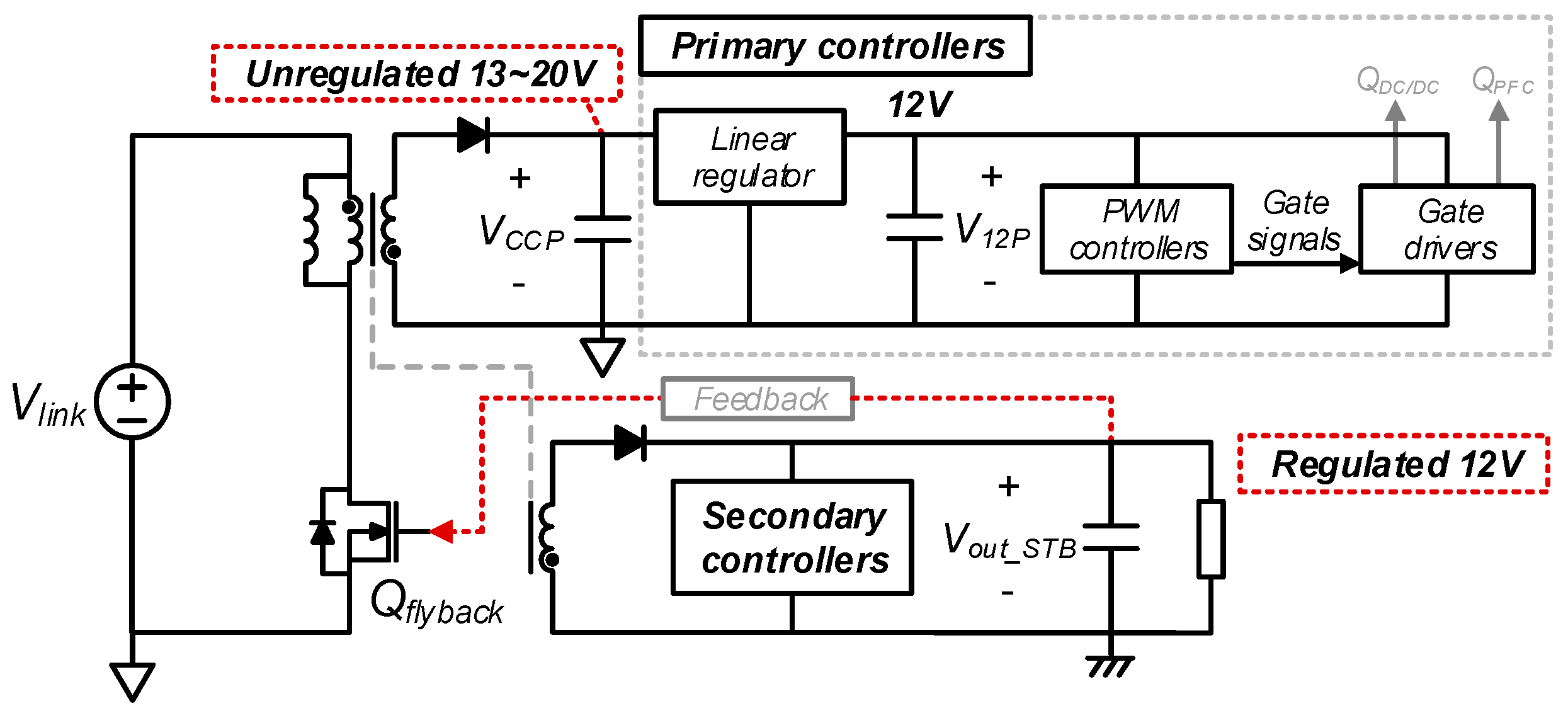
Figure 2 illustrates a simplified schematic of the standby converter and controllers. The standby converter provides standby output (
Vout_STB) and supply voltage for the controllers. The purpose of the
Vout_STB is to provide the output power to the server power system in the “standby state”. The output power of
Vout_STB is much smaller than the main output power. Usually, the standby output power is less than 30 W. This is because the standby output is used to maintain communication between the server power system and the power supply. Also, the secondary controller consumes a very small amount of power, such near 1 W. A microcontroller for communication and sequence control is powered by
Vout_STB. The server system should monitor its state always, even when the main power is turned off. In this case, only a small output power is required to monitor the system status, so only the standby flyback converter with a small output power rating provides the standby output power. For the standby output, the flyback converter is widely used because of its small size and wide input-range capability [
15,
16,
17,
18]. Since
Vout_STB should be regulated tightly, it is used for the feedback of the duty cycle of the standby converter.
Vout_STB is used for the standby output and the input power of the controllers on the secondary side. Also, the standby converter provides the input power of the controllers on the primary side. As shown in
Figure 2, the auxiliary turns are used for the primary side controllers. Due to cross-regulation issues, the supply voltage for the primary side controllers (
VCCP) cannot be regulated tightly, and
VCCP increases from 13 V to 20 V in a light load condition. For these reasons, a linear regulator is used to provide an accurate 12 V (
V12P) to the primary controllers. The loss of a linear regulator increases as
VCCP increases, because it is proportional to the difference between
VCCP and 12 V. Please note that the pulse-width-modulation (PWM) controller on the primary side cannot use
Vout_STB as its power source, because
Vout_STB is located on the secondary side. The primary side and the secondary side of the server power system should be isolated. As shown in
Figure 2,
Vout_STB and
V12P have different ground notation from each other [
18].
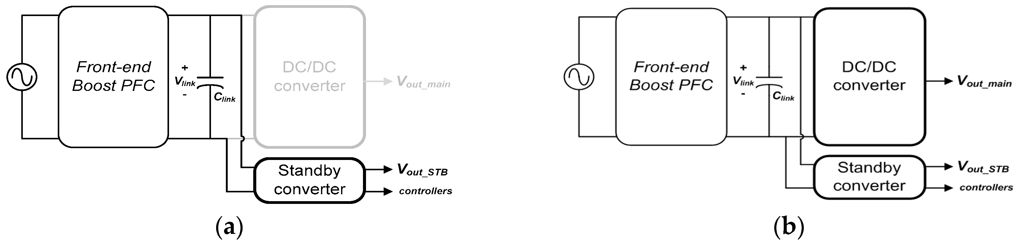
Figure 1a,b illustrates the standby mode and the normal mode of a server power supply. In the standby mode as shown in
Figure 1a, only the standby converter is turned on, and the DC/DC converter is turned off. Therefore,
Vout_STB and
VCCP are provided by the standby converter and
Vout_main is zero. In the normal mode as shown in
Figure 1b, the DC/DC converter is turned on and all outputs are provided. It should be noted that the losses of the standby flyback converter always exist regardless of operating mode. Therefore, the standby converter degrades the total system’s efficiency in entire load conditions [
15,
16,
17,
18,
19,
20]. Therefore, it is required to reduce the losses from the standby flyback converter. Furthermore,
VCCP increases in a light load condition due to the cross-regulation problem, and the losses from the linear regulator are also increased in a lighter load condition.
For these reasons, standby-flyback-integrating structures have been studied in recent years [
15,
16,
17,
18,
19,
20]. By integrating the flyback converter into the main power conversion stage, these works reduced switching losses, resulting in the improved efficiency of the system. However, approaches in [
15,
16,
17] require additional components and complex control signals. Also, the core loss of the flyback converter is always produced. Therefore, among the previous approaches, using an ORing diode [
19,
20] can be the simplest way to reduce the standby converter losses in applications where the
Vout_main and
Vout_STB are the same. However, just using an ORing diode [
20] cannot eliminate the losses from the flyback converter. This is because the standby flyback converter should provide
VCCP.
In order to completely eliminate the losses from the standby converter in the normal mode, [
19] proposed to turn off the standby converter. By using an ORing diode and an auxiliary winding, all outputs from the standby converter are provided by the DC/DC converter. Therefore, the standby converter can be turned off so that the standby losses can be eliminated. However, very important issues such as a steady state analysis, the transient responses, and how to control the standby converter are not discussed in [
19]. In this paper, further analysis on the technique is presented.
2. The Proposed Structure and Its Control Scheme
The proposed structure is shown in
Figure 3a. The PFC boost converter is omitted for simplicity, and it is assumed that the DC/DC converter has a constant input voltage (
Vlink). In order to provide
Vout_STB and supply voltage for the primary side controllers (
VCCP), the DC/DC converter uses a merging diode (
Dm), a small additional diode (
Da), and an auxiliary winding in the main transformer (
Naux) is used. The main purpose of the proposed structure is to turn off the standby flyback converter. In this case,
Vout_STB cannot be provided without
Dm.
Dm is used to connect
Vout_main to
Vout_STB, so that
Vout_STB can be provided even in the case where the standby flyback converter is turned off.
The secondary side controllers can also be powered by another additional winding. However, please note that the secondary side controllers do not need to be powered by the auxiliary winding, because the main output voltage is the same as the standby output voltage. Also, since Vout_STB should be regulated tightly, it is better to share the main output voltage. When another auxiliary winding is used, another additional regulator should be used in order to regulate Vout_STB, since the auxiliary winding cannot provide an exact voltage level.
In standby mode, the proposed structure operates the same as the conventional structure. The flyback converter provides Vout_STB and VCCP. The PSFB converter is turned off, since Vout_main has to be zero.
However, in the normal mode as shown in
Figure 2b, the flyback converter can be completely turned off after the PSFB converter is turned on. It can be noted that all of the outputs of the standby converter can be provided by the PSFB converter with the proposed structure.
Vout_main provides
Vout_STB using
Dm. Because the output current specification of the PSFB is much larger than that of the standby flyback converter, it is not a burden for the PSFB converter. Also,
Naux provides
VCCP using
Da. 2.1. Steady State Operation of the Proposed Structure in Normal Mode
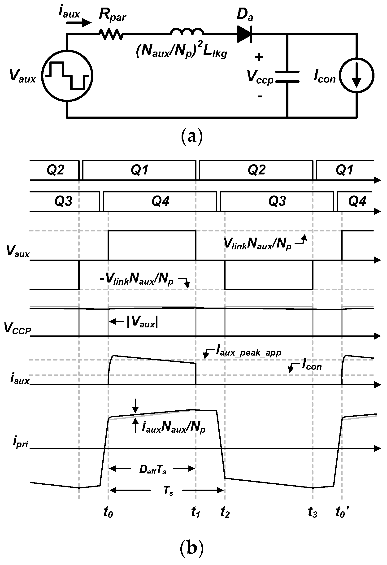
Figure 4a shows a simplified equivalent circuit for
VCCP. As shown in
Figure 4a, a parasitic resistance of auxiliary turn (
Rpar) and the reflected leakage inductance ((
Naux/
Np)
2Llkg) are connected in series with
Da, and the primary controllers can be regarded as a constant load current (
Icon).
Figure 4b shows the key waveforms of the proposed structure. As shown in
Figure 4b, voltage across the magnetizing inductance of the main transformer (
VLm) alternates between
Vlink and −
Vlink. Then, the voltage across the auxiliary winding (
Vaux) alternates between
VlinkNaux/
Np and −
VlinkNaux/
Np. Because
Da rectifies only a positive half cycle of
Vaux,
VCCP increases during
t0–
t1.
The auxiliary circuit operates as a resistor-inductor-capacitor (RLC) resonant circuit. However, the inductance can be neglected because
Np is much larger than
Naux in the PSFB converter. In this case, the circuit in
Figure 4a can be regarded as a switched capacitor circuit. The peak value of
iaux (
Iaux_peak_app) is determined by
Rpar. Assuming that the resistor-capacitor (RC) time constant of the circuit is much larger than the switching period of the PSFB,
iaux can be considered as a square waveform wave and its average value becomes
Icon. For these reasons,
VCCP and
Iaux_peak_app can be obtained by following Equations:
where
Deff is an effective duty-cycle in the PSFB converter.
Naux should be chosen to make VCCP larger than required voltage for the primary side controllers. A linear regulator can be used to provide a precise voltage for the controllers, following VCCP. In order to minimize the losses in the linear regulator, Naux should be minimized, satisfying the condition that VCCP should be larger than the required voltage for the controllers.
From (1), it should be noted that VCCP becomes constant regardless of the output condition with the proposed structure, whereas VCCP increases in a light load condition with the conventional structure, as mentioned in the introduction. Therefore, the losses from the linear regulator are also reduced in the proposed structure.
In the proposed structure, the primary current of the PSFB converter (ipri) is equal to the sum of iauxNaux/Np and the primary current in the conventional PSFB converter. However, ipri is almost same as the conventional PSFB converter; Icon is usually very small (much smaller than 1 A), and stepped down by the turns ratio Naux/Np. For these reasons, the proposed structure rarely affects the operation of the PSFB converter, so that the steady state characteristics of PSFB converter, such as the ZVS condition or effective duty cycle, are not affected.
2.2. Naux and Dm Selection
VCCP should be larger than V12P. This is because the linear regulator has a step down conversion ratio, so Naux should be large enough. On the other hand, in order to minimize the losses in the linear regulator, VCCP should be as small as possible. Therefore, Naux should be the minimum value satisfying VCCP > V12P. According to (1), it can be noted that Naux should be an integer value which is larger than NpV12P/Vlink.
In order to select Dm, consideration on the forward voltage drop of the merge diode is essential. The voltage regulation range of the server power supply is ±5% of the output voltage in this case. Therefore, the forward voltage drop should be smaller than its regulation range. The forward voltage drop of Dm should be smaller than its regulation range in the full load condition.
2.3. How to Disable the Standby Flyback Converter
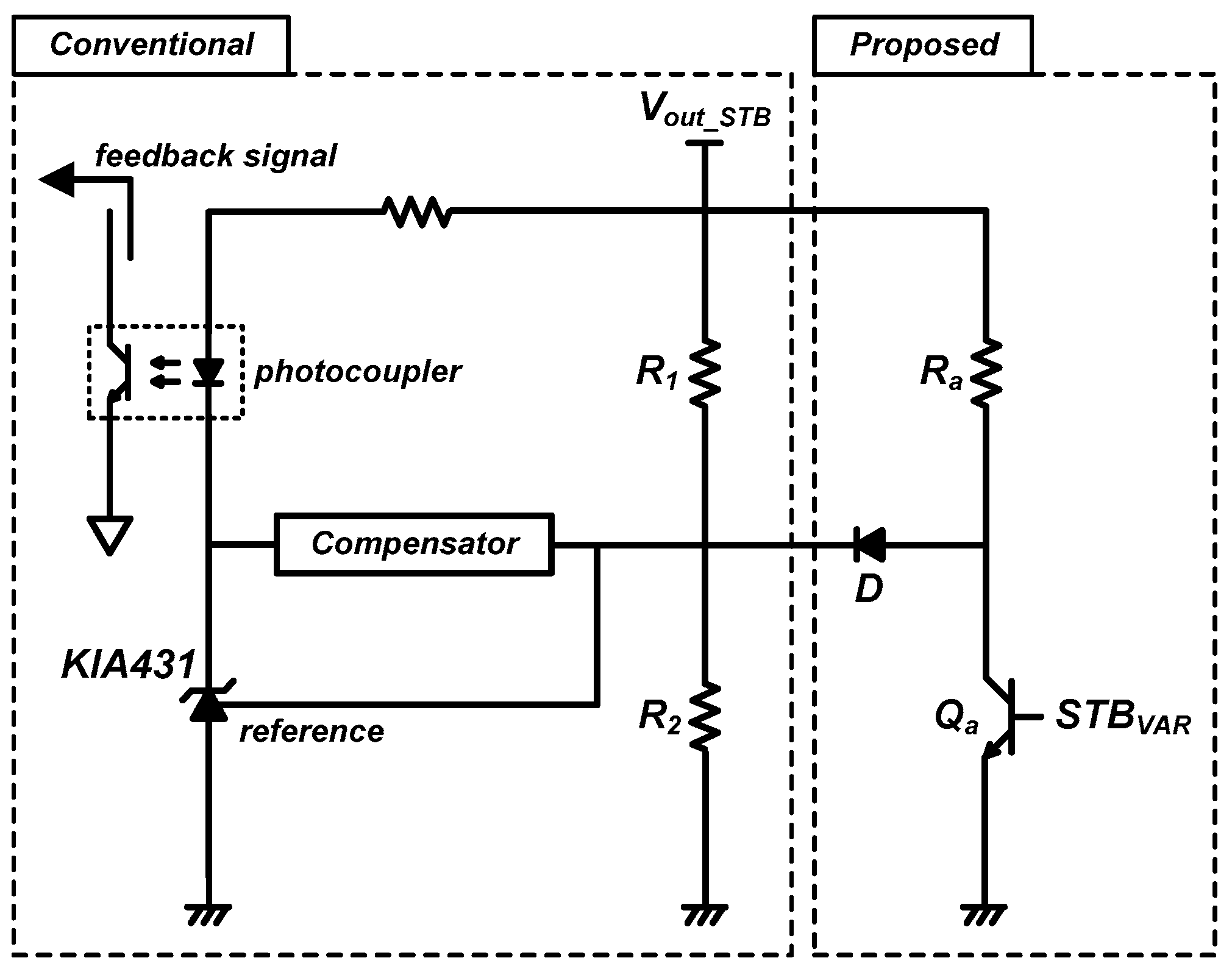
The standby flyback converter can be disabled with a simple addition to the feedback circuits.
Figure 5 shows the feedback circuit of the standby converter for the proposed structure. In the figure, the left side of the feedback circuit is for the conventional structure and the right side of the feedback circuit is proposed for the proposed structure. The added feedback circuit consists of an additional resistor
Ra, diode
D, and transistor
Qa, which is controlled by the
STBVAR signal. In standby mode,
Qa is turned on so that
D is turned off. The additional circuits do not affect the feedback circuit, since the additional circuits are separated from the conventional feedback circuit. However, in normal mode,
Qa is turned off and
D is conducted. Since
Ra is connected to
R1 in parallel and the reference voltage of the control loop becomes smaller, the feedback circuit operates as if
Vout_STB is larger than its appropriate value. In other words, the standby flyback converter is turned off.
2.4. Transient Response When Disabling the Standby Converter
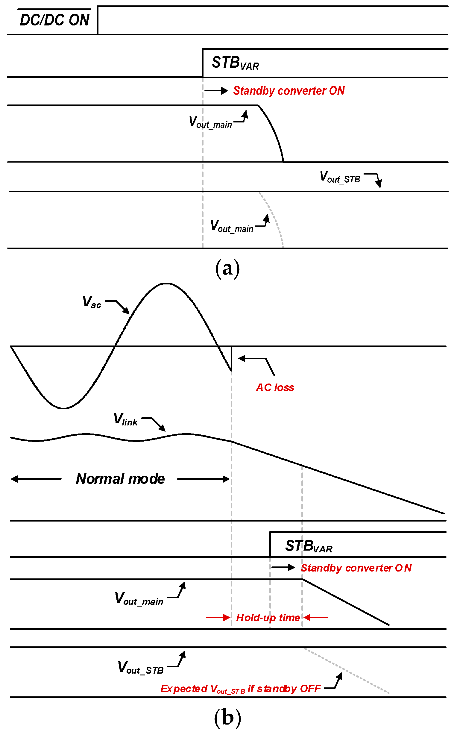
In the proposed structure, considerations on transient response are essential, since the flyback converter is turned on and off during its operation.
Figure 6 shows the disabling sequence for the standby flyback converter in normal mode. After the DC/DC converter is turned on,
Vout_main increases. The standby flyback converter should be turned off after
Vout_main is regulated. Otherwise,
Vout_STB will drop to
Vout_main. Therefore, the
STBVAR signal should be low after
Vout_main is regulated. In the proposed structure, the reference voltage is 2.5(1 +
R1/
R2) when the
STBVAR signal is high. However, when the
STBVAR signal becomes low,
Qa is turned off and the reference voltage of the controller loop becomes 2.5[1 + (
R1//
Ra)/
R2]. Therefore, the reference voltage decreases, and the expected value of
Vout_STB without a merge diode is 2.5[1 + (
R1//
Ra)/
R2].
2.5. Transient Response When Enabling the Standby Converter
There are two cases of shutdown in a server power supply. The first one is the DC/DC OFF case. In this case, the power system transits from the normal to the standby mode.
Figure 7a illustrates the DC/DC OFF case. Note that the DC/DC ON signal is active and low. The server computer requests DC/DC OFF and the DC/DC converter is turned off. After DC/DC OFF is requested by the server, the
STBVAR signal is enabled and the standby converter wakes up before the DC/DC converter is turned off.
The second one is the hold-up time. In general, a server power system should be able to regulate
Vout_main after the alternating current (AC) loss for tens of milliseconds, and it is called the hold-up time condition. During the hold-up time, the standby flyback converter should be enabled before
Vout_main decreases.
Figure 7b illustrates the key waveforms during the hold-up time. After AC loss occurs,
Vlink decreases and the PSFB converter regulates
Vout_main. After the hold-up time,
Vout_main decreases. The standby converter should be turned on within the hold-up time after the AC loss, so that
Vout_STB can be regulated by the standby converter even though
Vout_main decreases. If the standby converter is not turned on during the hold-up time,
Vout_STB should be decreased in the same way as
Vout_main.
2.6. Control of the STBVAR Signal
Figure 8 shows a flowchart for the
STBVAR signal. When the standby flyback is turned on, the system checks
Vout_main. If
Vout_main maintains at 12 V during a waiting time (
Tw), the
STBVAR signal is disabled to turn off the flyback converter. When the flyback is turned off, the system checks whether DC/DC OFF or any shutdown signals are produced. If the conditions are produced, the
STBVAR signal is enabled so that the flyback is turned on immediately. The pre-existing microcontroller is fast enough to provide the
STBVAR signal in time.
3. Experimental Results and Discussion
The feasibility of the proposed structure has been verified by a server power system with 12 V/62.5 A main output and 12 V/2.1 A standby output. The system is designed with
Np = 26,
Ns1 =
Ns2 = 1,
Naux = 1, and
Llkg = 15 μH. ES1D (200 V, 1 A, DO-214AC) is selected for
Da, M2FM3 (30 V, 6 A, M2F) is selected for the merge diode
Dm, and ICE3AR0680JZ is selected for the standby flyback converter. The voltage regulation range of the server power supply is ±5% of the output voltage in this case. Therefore,
Vout_main and
Vout_STB should be regulated within 11.4–12.6V. Since the forward voltage drop of
Dm is less than 0.4 V as the maximum value, it can be said that the forward voltage drop of the merge diode does not affect the regulation of
Vout_STB.
Figure 9 shows the implementation of the proposed structure. It can be noted that the auxiliary turn occupies a very small window area, so that it does not affect the design of the transformer. In addition, the merging diode
Dm is very small so that the power density of the total system is not degraded.
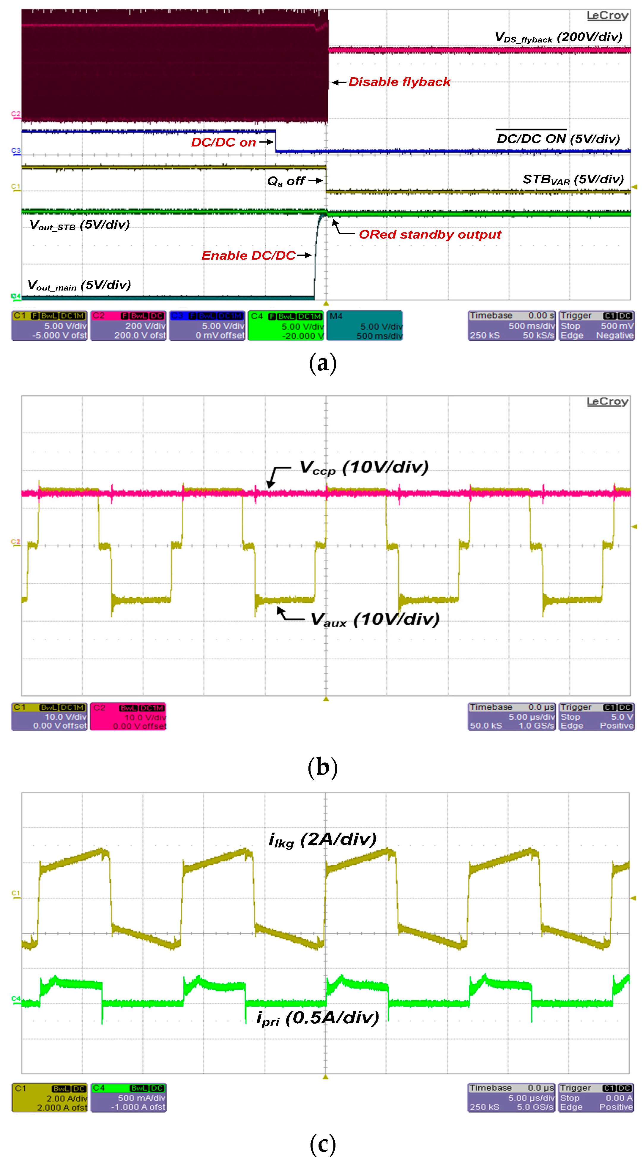
Figure 10 shows the experimental waveforms of the proposed structure at full load condition in normal mode.
Figure 10a shows the disabling sequence of the standby flyback converter.
VDS_flyback represents the drain-to-source voltage of the main switch of the standby flyback converter. When the standby flyback converter is turned on,
VDS_flyback alterantes between zero and its peak value. In order to present the sequence clearly, the time division of the waveforms is set to 500 ms/div. Because the switching period of the standby converter is much shorter than the division,
VDS_flyback occupies the black area in the figure when the standby converter is turned on. Negative
DC/DC ON represents the control signal for
Vout_main provided by the server system. Note that the signal is active and low, so that the LOW signal means that the server system commands the DC/DC converter to be turned on, and the HIGH signal means the system commands the DC/DC converter to be turned to OFF. Generally, one or two seconds are enough for the building/collapsing time after the DC/DC controlling signal is applied, although the time depends on the power supply vendor. As shown in
Figure 10a, after
DC/DC OFF becomes low, the DC/DC converter is turned on and
Vout_main increases. After
Vout_main is regulated, the
STBVAR signal becomes low to turn off the standby converter.
Figure 10b,c shows the waveforms for
Vaux,
VCCP,
ipri, and
iaux in a full load condition after the standby converter is turned off.
VCCP is provided by
Naux as shown in
Figure 10b.
Naux provides 14 V of
Vccp so that the primary controllers can operate with 12 V input voltage, following a linear regulator. In the proposed structure, as shown in
Figure 10c,
ipri of the PSFB converter is almost the same as that of the conventional one as mentioned before. Therefore, it can be noted that the proposed structure does not affect the efficiency of the PSFB converter.
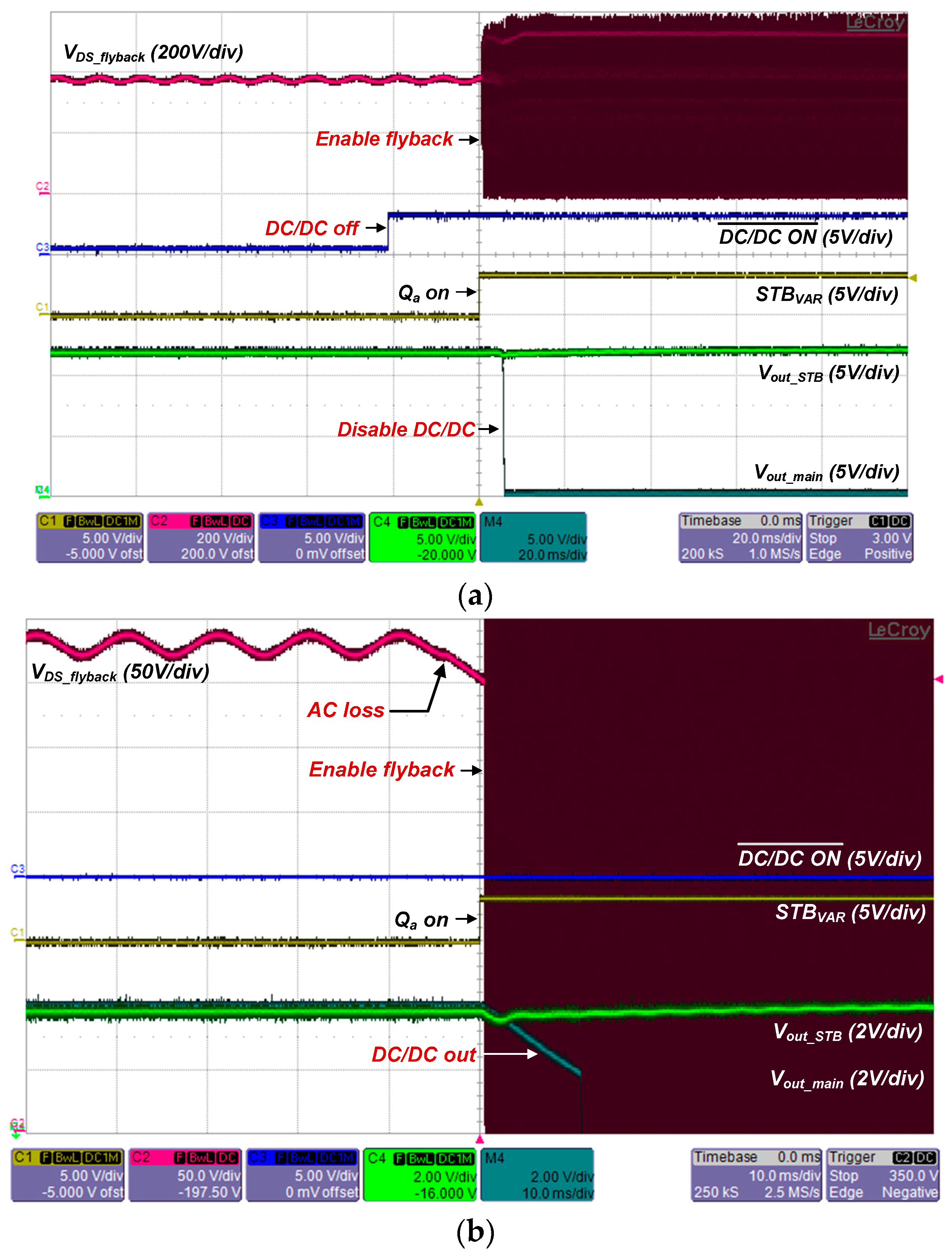
Figure 11a illlustrates the experimental waveforms in the DC/DC OFF case. When the
DC/DC OFF signal is applied, the
STBVAR signal is enabled and the standby converter wakes up to provide
Vout_STB, and then the PSFB converter is turned off and
Vout_main is zero while
Vout_STB is adequately provided.
Figure 11b shows the waveforms during the hold-up time. After AC loss occurs,
Vlink decreases and the
STBVAR signal becomes high to turn on the standby converter. The standby converter is turned on before
Vout_main decreases, so that
Vout_STB can be stable during the full load transition.
Figure 12a,b shows the measured loss from the standby converter with the conventional structure (only the ORing diode has been implemented) and the efficiency of the proposed structure, respectively. From
Figure 12a, it can be noted that the standby converter produces about 1.5 W of losses in entire load conditions. Furthermore, due to the cross regulation problem of the flyback converter, the losses from the standby stage are larger than 1.5 W. The standby converter is designed to have the boundary between the continuous conduction mode (CCM) and the discontinuous conduction mode (DCM) near 60% load condition. In a higher than 70% load condition, the flyback converter operates in continuous conduction mode (CCM). The flyback converter in DCM operation operates with valley switching. On the other hand, the flyback converter in CCM operates with full hard switching. Since the standby converter has higher switching loss in CCM operation, the standby converter has larger losses in a higher than 70% load condition. In the proposed structure, since the PSFB converter provides all outputs of the standby flyback converter with much higher efficiency, the system efficiency increases in the entire load condition, as shown in
Figure 12b. It should be noted that the efficiency is improved in entire load conditions, and the efficiency improvement is larger than the losses from the standby converter, since the proposed structure also reduced the losses from the linear regulator on the primary side.
Table 1 represents the comparison of loss components between the proposed work and the previous works in normal mode operation. As shown in the table, it can be noted that the previous works [
15,
16,
17] have a switch, transformer, and rectifier diode as the loss components related to
Vout_STB in normal mode operation. On the other hand, the proposed structure has only two merge diodes (
Da,
Dm) as the loss components in normal mode operation, because the standby converter is in the off-state by STBvar. That is, the losses in the previous works have not occurred in the proposed standby structure. Therefore, it can be said that the proposed structure can achieve a higher efficiency compared to the previous works.


