A Digitally Controlled Power Converter for an Electrostatic Precipitator
by
 , , , and
Pedro J. Villegas
* ,
,
Juan A. Martín-Ramos
 ,
,
Juan Díaz
,
Juan Á. Martínez
,
Miguel J. Prieto
and
Alberto M. Pernía

Department of Electrical Engineering, University of Oviedo, 33204 Gijón, Asturias, Spain
*
Author to whom correspondence should be addressed.
Energies 2017, 10(12), 2150; https://doi.org/10.3390/en10122150
Submission received: 13 October 2017
/
Revised: 11 December 2017
/
Accepted: 12 December 2017
/
Published: 15 December 2017
Abstract
:Electrostatic precipitators (ESPs) are devices used in industry to eliminate polluting particles in gases. In order to supply them, an interface must be included between the three-phase main line and the required high DC voltage of tens of kilovolts. This paper describes an 80-kW power supply for such an application. Its structure is based on the series parallel resonant converter with a capacitor as output filter (PRC-LCC), which can adequately cope with the parasitic elements of the step-up transformer involved. The physical implementation of the prototype includes the use of silicon carbide—SiC—semiconductors, which provide better switching capabilities than their traditional silicon—Si—counterparts. As a result, a new control strategy results as a better alternative in which the resonant current is maintained in phase with the first harmonic of the inverter voltage. Although this operation mode imposes hard switching in one of the inverter legs, it minimizes the reactive energy that circulates through the resonant tank, the resonant current amplitude itself and the switching losses. Overall efficiency of the converter benefits from this. These ideas are supported mathematically using the steady state and dynamic models of the topology. They are confirmed with experimental measurements that include waveforms, Bode plots and thermal behavior. The experimental setup delivers 80 kW with an estimated efficiency of 98%.
1. Introduction
ESPs have been industrially used to eliminate polluting particles in gases since the beginning of the 20th century [1,2,3,4]. They are durable, relatively simple to maintain, cost-effective and present a high collection efficiency, typically 80% per step. ESPs have found application in power generation plants, steelworks, cement-free building materials, chemical process factories, incinerators, etc. Thus, by using three steps placed in series, it is possible to reach an efficiency in particle elimination above 99%. Its mode of operation is as follows: A very high DC voltage of 45–150 kV negative is applied to a wire located in the center of the precipitator, known as a discharge electrode. The outer walls of the precipitator, called the collector electrode, are grounded to zero potential. The gas to be purified is injected through the precipitator. The electric field around the wire reaches high enough values to cause a discharge crown, ionizing the gas around it and injecting electrons. Negative electrons and ions are accelerated by the electric field to the collector electrode. By collision and ion capture, particles suspended in the gas are charged and also deposited by the electric field in the collector electrode. The gas then exits the precipitator free of impurities. Since particles larger than 10 µm in diameter absorb several times more load than those smaller than 1 µm, the electrical forces are much lower in the latter. As the particles begin to settle into the collector, the thickness of the material layer in the collector increases. As a consequence, the electric field decreases, so it is necessary to periodically clean the collector surfaces. The material falls and collects at the bottom.
The complete filtrate is divided into several sections that are sequentially crossed by the gas. Each of them is controlled by a different voltage source and can be considered an independent precipitator. Depending on the physical proportions of each section and the power and voltage levels applied, different harvesting efficiencies are achieved in each section. They are generally optimized for dust collection of different sizes. The sum of the individual performances gives the final total performance figure for the system. For it to reach 99% the precipitator must have three or more sections.
They must be supplied by using a DC power source that provides around 100 kV and 100 kW to the ESP electrodes. The design of such power sources commonly relies on low-frequency phase regulators [5]. A typical structure includes thyristors, low frequency transformers working at 50–60 Hz, and a rectifier bridge at the output. A coil in series limits the current peaks in the input when a short circuit occurs at the output. These short circuits are frequent (up to 90 per minute) due to the dielectric rupture of the gas flowing through the ESP electrodes. In this sort of DC power sources, the triggering of the thyristors regulates the average voltage level at the electrodes. One of the problems associated to this technique is the very large low-frequency ripple it gives rise to [6], which makes the change to High Frequency Switched Mode Power Supplies (HF-SMPS) become a very attractive solution for ESPs. Some of the advantages are:
- Reduction of weight and volume due to the use of high frequency in the step-up transformer.
- Decrease of the volume of oil in the tank containing the high-voltage equipment, i.e., the transformer and the rectifier output.
- Better performance from the point of view of the input network because of its three-phase connection and its higher power factor (above 0.9).
- Operation independent of the input frequency.
- Lower ripple at the output voltage for a given specification of the precipitator. This is so because the output capacitance between the electrodes remains the same, whereas the output rectifier frequency experiments a great increment. Additionally, this ripple reduction means an increment in the average output voltage for the same peak (breakdown) in the operating voltage.
- Possibility to supply the ESP with pure DC voltage, or to include different pulses or degrees of intermittency due to the source faster dynamic response.
Despite all these advantages, the construction of high-frequency power sources was not addressed until the last decade, due to problems related to the design of equipment involving high current levels [7,8]. Nowadays, its use is still incipient [5] with limitations in voltage (less than 80 kV) and current (less than 1 A). With the advantages provided by HF-SMPS, the ESP itself may evolve to operate with new voltage waveforms that are more convenient from the process point of view. New operating capabilities can provide greater purification efficiency. The effect of these new sources is even more evident in cases where the phenomenon of “back corona” appears. This phenomenon, generally linked to high-resistivity impurities [9], takes place when the potential drop across the dust layer is so large that corona discharges begin to appear in the gas trapped within the dust layer.
In [10,11] a series-parallel resonant tank (SPRC) and IGBTs as the switch are used to implement the ESP. In this paper, a series-parallel resonant converter (PRC-LCC) as HF-SMPS is proposed and studied for ESPs. Additionally, a “new” control strategy is also proposed that minimizes reactive energy through the resonant tank and improves the switching losses by using SiC MOSFETs. Two versions of the inverter (Si IGBTs vs. SiC MOSFETS) have been assembled in order to compare their features. Their output voltage and power are regulated by means of only one control variable: the duty cycle, d. The design of the closed-loop operation is based on the topology small signal model developed.
2. The Model for the Series-Parallel Topology
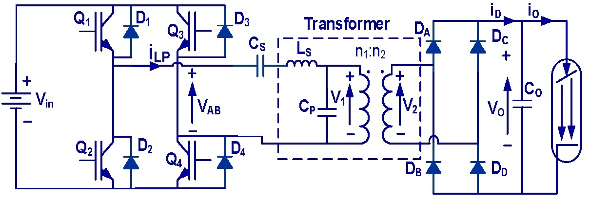
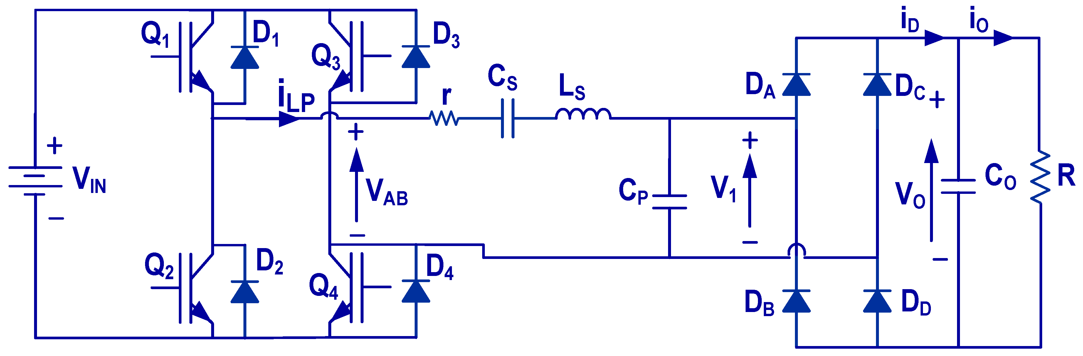
2.1. Power Stage
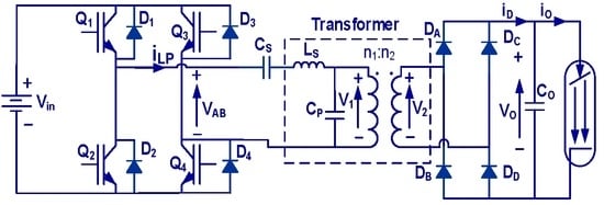
There are several resonant topologies described in the literature [12,13,14,15] that use LCC resonant tanks, i.e., LLC resonant converter [16], soft switching technology [17] and a secondary-side resonant converter [18]. But the series-parallel resonant converter (PRC-LCC) with an inductive output filter is especially well suited for the type of application considered in this paper [19]. This topology has, however, one drawback in our case: it is not easy to design the inductor in the output filter when the output voltage is very high. Thus, for the sake of simplicity, many high-output DC voltage applications use a PRC-LCC resonant topology with only a capacitor as output filter, as shown in Figure 1 [20,21,22,23]. The price to pay for this simplification in the assembly is a more complicated performance of the topology, since the use of a purely capacitive filter results in discontinuous-conduction-mode operation. Nevertheless, this is not much of a problem, for the behavior of this topology has already been described and developed by means of different mathematical models for a half-bridge [20,24] where several topologies are compared, for a PRC-LCC topology [21,23,25,26]; for high voltage pulse loads [22] and full bridge Zero Current Switching Pulse Wide Modulation (ZCS PWM) application in [27]. Other models have been developed in [28,29,30,31] for LCC-type parallel resonant converter.
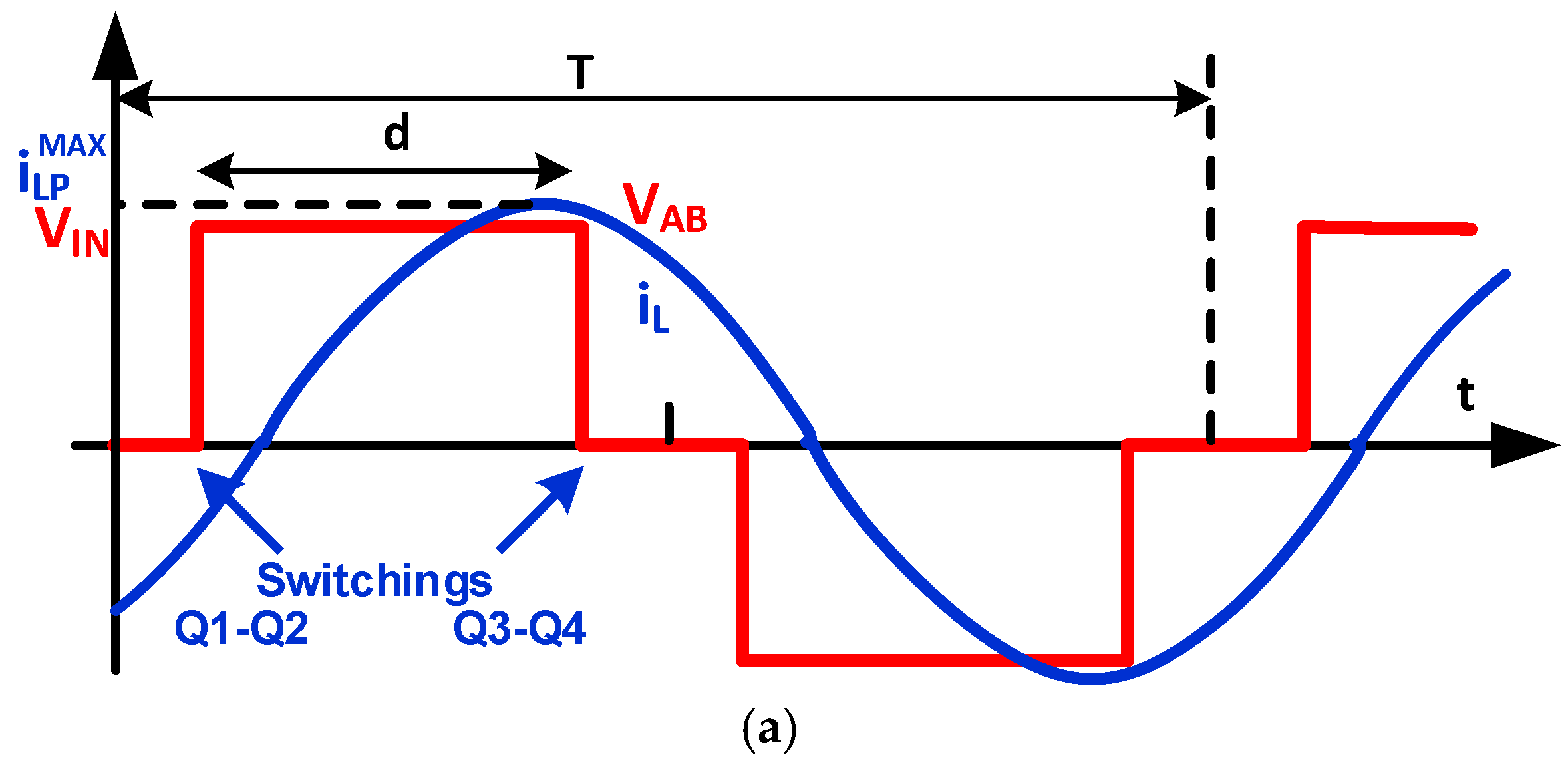
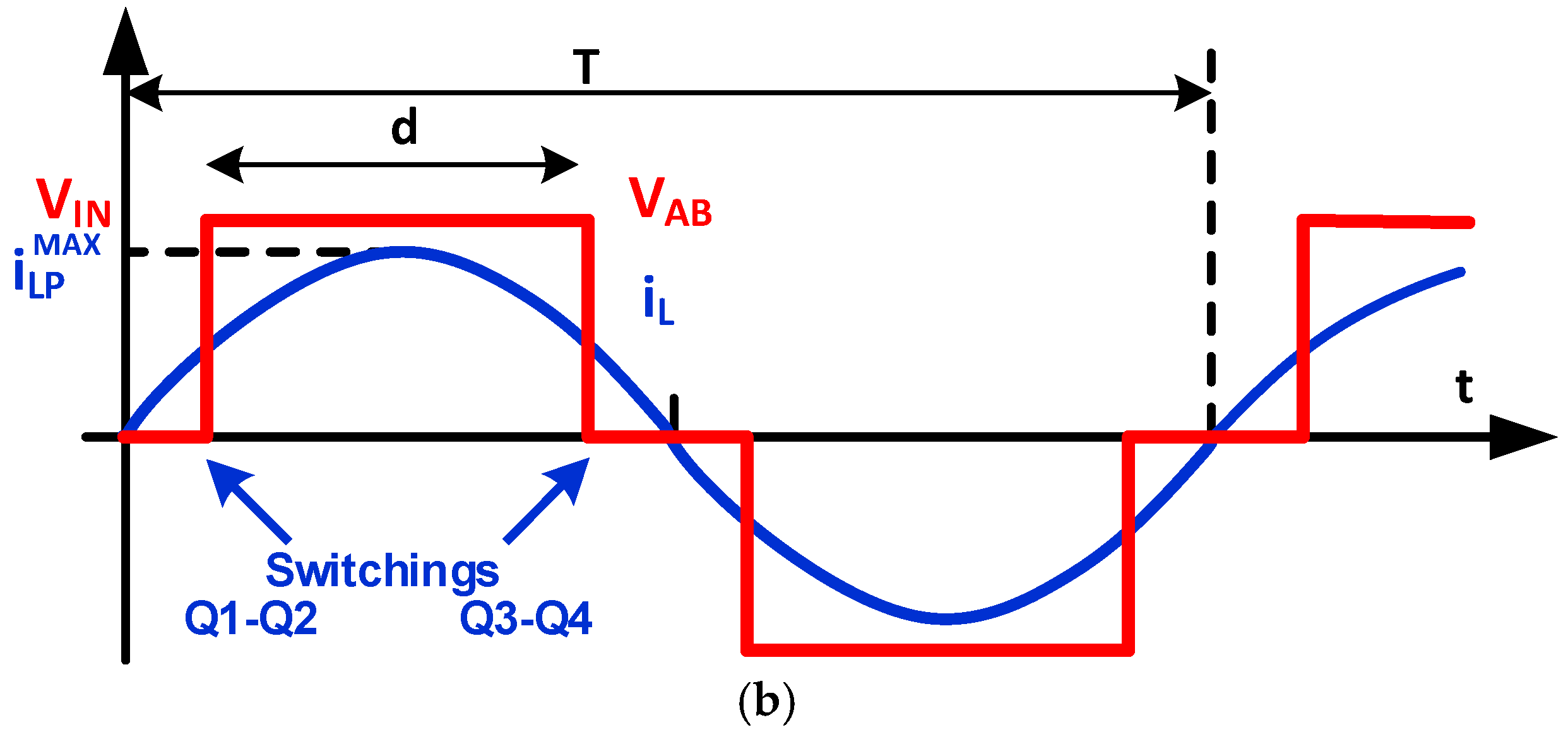
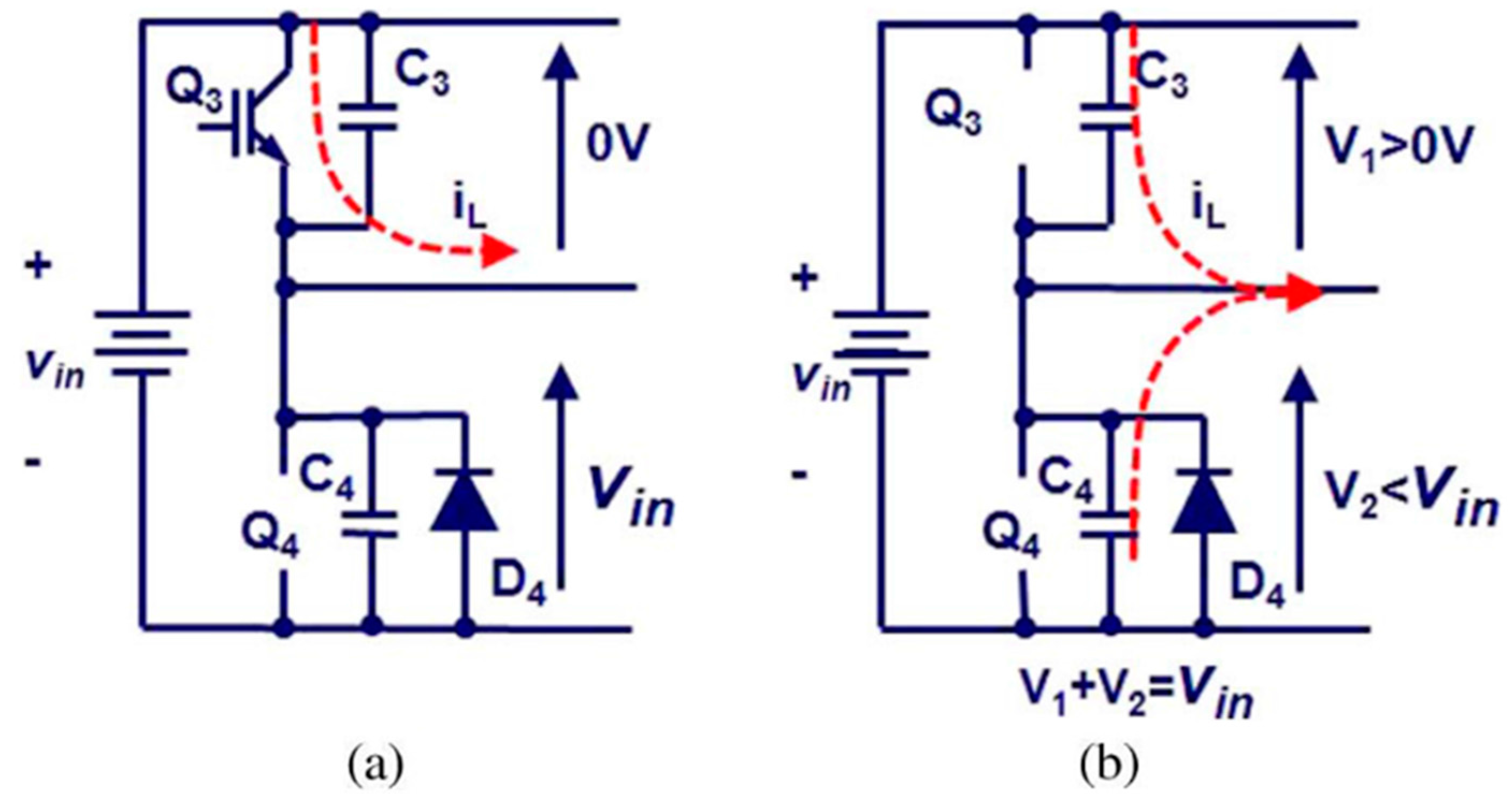
In the optimal current control traditionally used (Figure 2a), the current through the resonant tank, iL, is high because it has a reactive component, due to the fact that it is not in phase with the input voltage to the tank, VAB. On the other hand, the switching current of the switches Q3–Q4 is much greater than that in switches Q1–Q2, and, therefore, so are the switching losses.
In the centered current control (Figure 2b), the resonant current, iL, is smaller than the one obtained with the optimal current control, since this current is in phase with the input voltage, VAB. This allows conduction losses to be reduced. On the other hand, for high duty cycles, the switching currents will be similar in both legs of the inverter, and smaller than those produced in the optimal current control (Figure 2a); these results in lower switching losses. In this paper, the control mode used sets a switching frequency that guarantees that the inverter is working in the centered current mode.
2.2. Large-Signal Model and Steady-State Condition
Not all the models describing the performance of a PRC-LCC with capacitive output filter are equally easy to work with [32]. In some cases, different operation regions are identified in the performance of the topology. Each of these regions is adequately modeled, but the only way to identify the operation region the converter that is working is by means of a trial-and-error procedure. This is not practical to carry out a full analysis of the converter, mainly because the adequate set of equations to be used is not known at the beginning of the calculation.
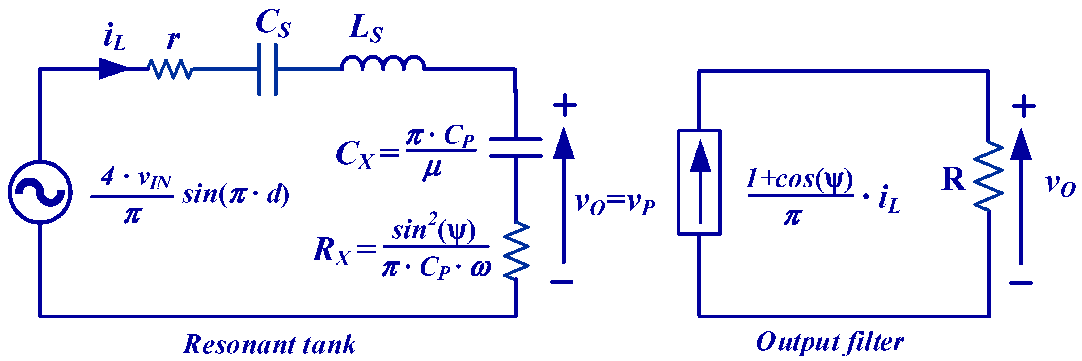
There is one model, however, that succeeds in describing the full performance of the topology throughout its continuous conduction mode using a single set of equations [25,33]. This model can be used for large-signal, small-signal and steady-state analysis. Focusing on the latter, a simple equivalent circuit can be used to represent steady-state performance (Figure 3); reference [32] provides the details on how to obtain such an equivalent circuit. This steady-state model is better suited than those defining different operation regions, for it results in a set of equations that can be used for the whole range of operation (at steady state); these equations can also be adapted to any control mode.
Any practical application provides the specification of the input DC voltage, VIN, the output DC voltage, VO, and the output power, PO. On the other side, after assembling the power supply, the values for all the circuit components (r, LS, CS, CP, and R) are known [25,33]. The equivalent load of the converter, R, is derived from the output voltage and output power specifications, and its value is typically considered to be constant.
An impedance analyzer may measure the other parameters of the topology: r is the parasitic resistance of the circuit; CS is a serial capacitor; LS and CP are, respectively, the parasitic inductance and capacitance of the step-up transformer. All those parameters are referred to primary by using the transformer turns ratio. With these data, the mathematical model provides a method to calculate a suitable value for the control parameters.
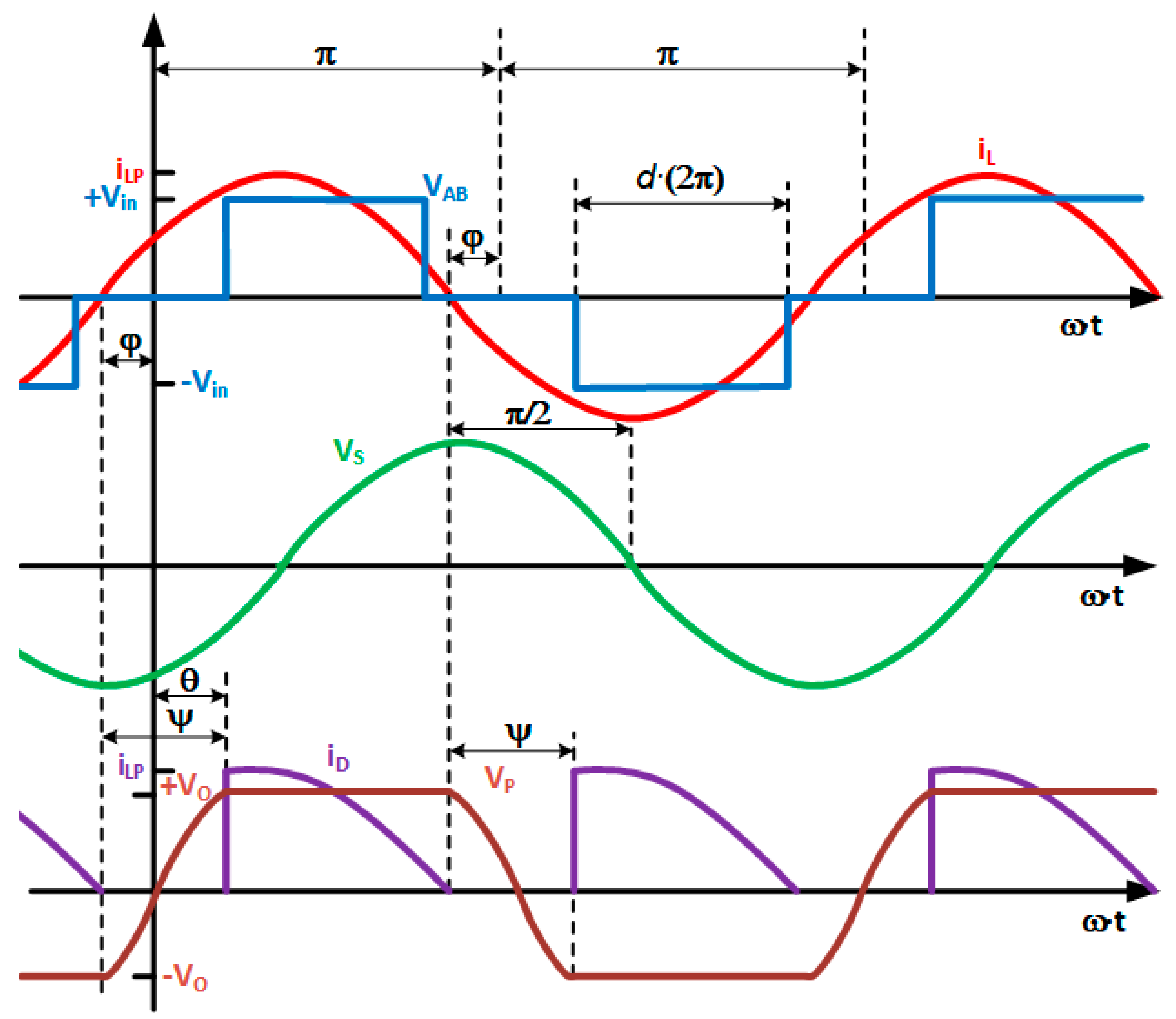
In Figure 3, CX and RX depend on μ, which is simply a function of the clamping angle Ψ (1) used for the sake of compactness. The clamping angle, Ψ, varies between 0 and π radians and has a physical meaning: it represents the part of the period where none of the output rectifying diodes is on (see Figure 4). During this period, CP provides all of the resonant current, iL, while experiencing a voltage variation from –VO to +VO (or vice versa). These conditions provide the way to calculate Ψ (2) [31]. Since R and CP are previously known, only ωS needs to be obtained in order to derive the value of the clamping angle:
Figure 3 shows two differentiated circuits. The one on the left represents the topology resonant tank, where several components are connected in series whose impedance is:
The control method must maintain the sinusoidal current centered with respect to the inverter voltage. This means that the first harmonic term of the voltage and the resonant current must be in phase, ϕ = 0 (Figure 4). This condition is met if the imaginary part of the resonant network is null (ZIMAG = 0) for the switching frequency, fS. Since ZIMAG is defined in (5), it can be solved for fS as shown in (6). However, it must be noted that fS depends on CX, and, thus, on Ψ:
The procedure described so far has resulted in two equations, (2) and (6), with only two unknown variables, Ψ and ωS. There are different ways to calculate the value of these unknowns. One possibility is using a look-up table. Other possibility consists in applying recursive methods. When using the latter option, a value for Ψ is inserted in (6) so as to obtain ωS; then (2) is used to check whether the value thus obtained is correct and, after some iteration, the solution is found.
Now that fS and Ψ are known, the impedance of the resonant network is obtained through (3), since:
In the resonant tank of Figure 3, it makes sense to consider the energy balance in the circuit. Most of the power is transferred from the power source to resistor RX. This power on RX ideally equals the output power, PO. Hence, (8) provides an expression for the amplitude of the resonant current, .
Now, Kirchhoff’s law is applied to obtain the required input voltage (9).
Finally, the duty cycle is calculated from the relationship between the DC input voltage, VIN, defined in Figure 1, and the first harmonic term of the output voltage of the converter, VAB, as in (10):
By following this procedure, the control parameters (duty cycle and frequency) can be obtained for any required operation point.
2.3. Centered-Current Operating Point
Overall losses have been estimated on real prototypes considering two different types of switches: IGBT (FF300R12KS4) and SiC MOSFET (CAS300M12BM2).
The working conditions in the prototypes tested were:
- -
- VIN = 800 V, VO = 80 kV (1000 V in the primary side) and PO = 80 kW (R = 12.5 Ω in the primary side).
- -
- Transformer parameters: n1/n2 = 1/80, LS = 62.7 μH, CP = 219 nF (see Figure 5). A series capacitor CS = 408 nF completes the topology.
Once the switching frequency has been decided and the converter is working on the centered-current mode, the duty cycle (d) is used to regulate the output voltage (VO). This control scheme is referred to as centered-current control. By using this control mode, each of the legs of the inverter has a different switching pattern. One of them, Q1–Q2, experiences hard-switching (Figure 6), whereas the other one, Q3–Q4, goes through zero voltage switching (ZVS) thanks to the conduction of the diodes in parallel (Figure 7).
In order to calculate switching losses, it is necessary to know the value of the actual switching current through the semiconductors, IS, the switching frequency, fS, the input voltage, VIN, and the switching energies in the semiconductors when operating at nominal voltage and current (VN = 600 V and IN = 300 A in this case).
Since this paper considers two different types of semiconductors, the energies to use in the calculation of the switching losses are:
- IGBT: EON(IGBT), EOFF(IGBT)
- IGBT diode: EREC(DIGBT)
- MOSFET SiC: EON(MOS), EOFF(MOS)
- MOSFET SiC diode: EREC(DMOS)
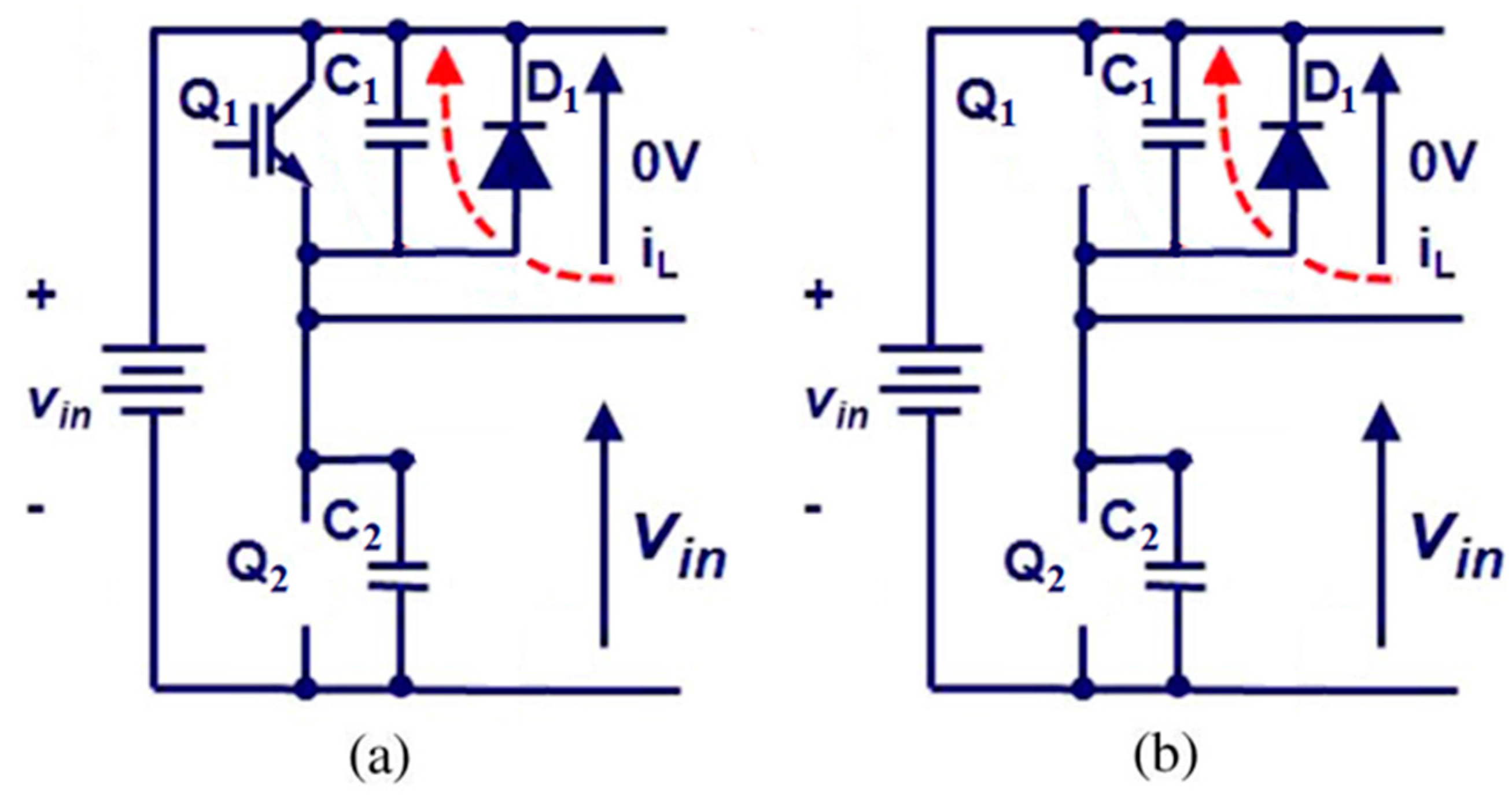
As indicated in Figure 6, switch Q4 turns on with no losses, but there are switching losses in Q3 when it is turned off. Leg Q1–Q2 performs differently (Figure 7): Q1 turns OFF with no losses, because the diode in parallel, D1, is ON; switching losses appear when Q2 turns ON and diode D1 is forced OFF. The formula to estimate these losses is given by (11):
Conduction losses can be calculated by applying Equation (12). The magnitudes included in this expression are:
- The average, IAVG, and RMS, IRMS, values of the current circulating through the switches.
- The forward voltage drop, VD, or the ON resistance, RCD, of the semiconductor:
- IGBT: VCESAT(IGBT), RCESAT(IGBT)
- IGBT diode: VF(IGBT), RD(IGBT)
- SiC MOSFET: RDS(MOS)
One important matter to consider is the importance of the diodes. When using IGBTs, the diodes in anti-parallel are ON during a sizeable part of the switching period, whereas with SiC MOSFETs they are only ON during the dead times of the legs, when no switch is ON.
In the theoretical analysis, the current and voltage levels in the inverter have been obtained from the topology steady-state model. Later, the theoretical values will be proven to be similar to experimental ones.
The operating point has been calculated using Equations (1)–(10) at nominal conditions:
- VIN = 800 V, VO = 80 kV (1000 V in the primary side) and PO = 80 kW (R = 12.5 Ω in the primary side).
The values obtained for the experimental operating point are as follows:
- Amplitude of the resonant current iPL = 171 A, switching current for leg Q1–Q2 IS = 52.5 A, switching current for leg Q3–Q4 IS = 78.7 A, switching frequency fS = 37.7 kHz and duty cycle d = 0.388.
The losses in the switches haven been obtained through calculation, using Equations (11) and (12), the values previously obtained for the nominal operating point and the parameters provided by the manufacturers in their datasheets.
- IGBT: EON(IGBT) = 36 mJ, EOFF(IGBT) = 18 mJ
- IGBT diode: EREC(DIGBT) = 13 mJ
- MOSFET SiC: EON(MOS) = 8.75 mJ, EOFF(MOS) = 5.95 mJ
- MOSFET SiC diode: EREC(MOS) = 1.92 mJ
- IGBT: VCESAT(IGBT) = 1.2 V, RCESAT(IGBT) = 5.75 mΩ
- IGBT diode: VF(IGBT) = 1.5 V, RD(IGBT) = 1.6 mΩ
- SiC MOSFET: RDS(MOS) = 5 mΩ
The estimated total losses for a full bridge, Table 1, made with IGBTs are 2.54 kW in total: 1.71 kW associated to leg Q1–Q2 and 836 W coming from leg Q3–Q4. This level of losses requires that two inverters be parallelized in order to share them. If SiC MOSFETs are used instead, losses in the inverter are reduced to 740 W, with PQ1–Q2 = 503 W and PQ3–Q4 = 237 W, below 1% the total delivered power.
2.4. Small Signal Model
The Bode diagram of the inverter expresses the dynamic relationship between the controlled variable, the output voltage, and the control parameter, the duty cycle (13)
Transfer function, G(s), has been obtained by modifying the small-signal model of the topology presented in [25] so as to include the control strategy in the mathematical equations. This strategy sets a constant switching frequency so that the resonant current is centered with respect to the inverter voltage, Figure 8. The duty cycle, d, controls the output voltage VO.
The mathematical model was implemented using MATLAB (R2015b, MathWorks, Boston, MA, USA) Equation (14), which allowed the theoretical Bode diagram of the converter to be plotted (blue line in Figure 9).
A scaled prototype, Figure 10, was assembled to validate the theoretical Bode plot. It is a 10:1 version, in voltage and current, of the final power supply: VIN = 80 V, VO = 100 V, fS = 38 kHz, R = 12.5 Ω, CO = 96 μF and PO = 800 W. All the variables have been transferred to the primary of the transformer. Transformer parasitics, LS and CP, have been implemented using discrete components. In this case, an analogue circuit implements the phase-shifted control. This gain must be considered when comparing experimental measurement and theoretical prediction.
Figure 9 also shows the experimental small signal behavior of the prototype (in orange). Data are captured by means of a differential probe and a data acquisition card as explained in [34]. The difference between the mathematical calculation and the experimental measurement is not significant. It is important to remember that any theoretical small signal model should be valid up to one tenth of the switching frequency, i.e., up to 4 kHz in this case.
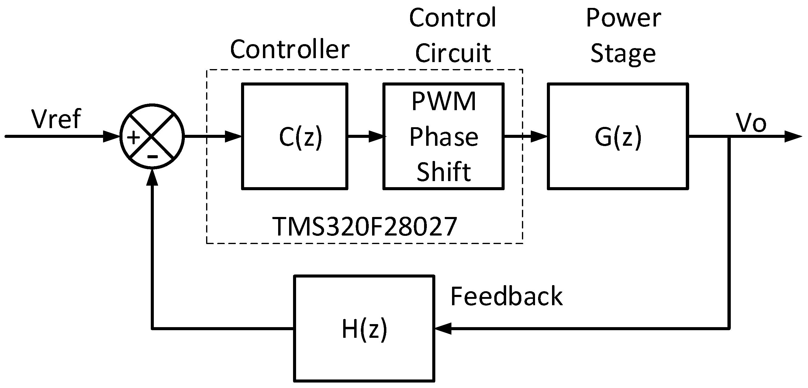
The authors in a previous work [33] performed the control of the converter with an analog control, C(jω). In this work, the design of the digital feedback loop [35,36] is based on classical control theory and small signal analysis (Figure 11). Other techniques based in digitally controlled power converter based on DSP [10] could be used always. All the transfer functions used have been discretized using the ZOH approximation with TS = 1/fS. Since the output voltage, VO in Figure 10, is floating, a differential amplifier is used to feedback the output voltage, H(z). The Bode diagram of the inverter is G(z). Its differential gain is 31.25 × 10⁻⁶ and it presents a high-frequency pole at 4 kHz to eliminate noise. The regulator, C(z), introduces a proportional integral action, PI, (15). The pole at the origin guarantees the absence of a position error. The regulator’s gain is set to provide enough phase margin, 64.5 degrees, and a bandwidth of 502 Hz. Altogether, this decision avoids dangerous oscillations in the output voltage (Figure 12):
3. Experimental Results
The converter has been tested experimentally as shown in Figure 12. Actual waveforms and their values match theoretical ones. Figure 13 shows a picture of the test bench. A TMS320F28027 digital microcontroller (Copyright © 2010, Texas Instruments Incorporated, Dallas, TX, USA) is used to implement the phase-shift control and the digital regulator C(z).
It must be noted that the power switches, the output rectifier, DA–DD, and a three-phase input rectifier have been installed on the heatsink shown in the figure (the three-phase rectifier together with a filter capacitor allows voltage VIN to be obtained from the three-phase mains). The temperature of the heatsink will increase due to the losses in the switches and in both rectifiers. The nominal conditions are:
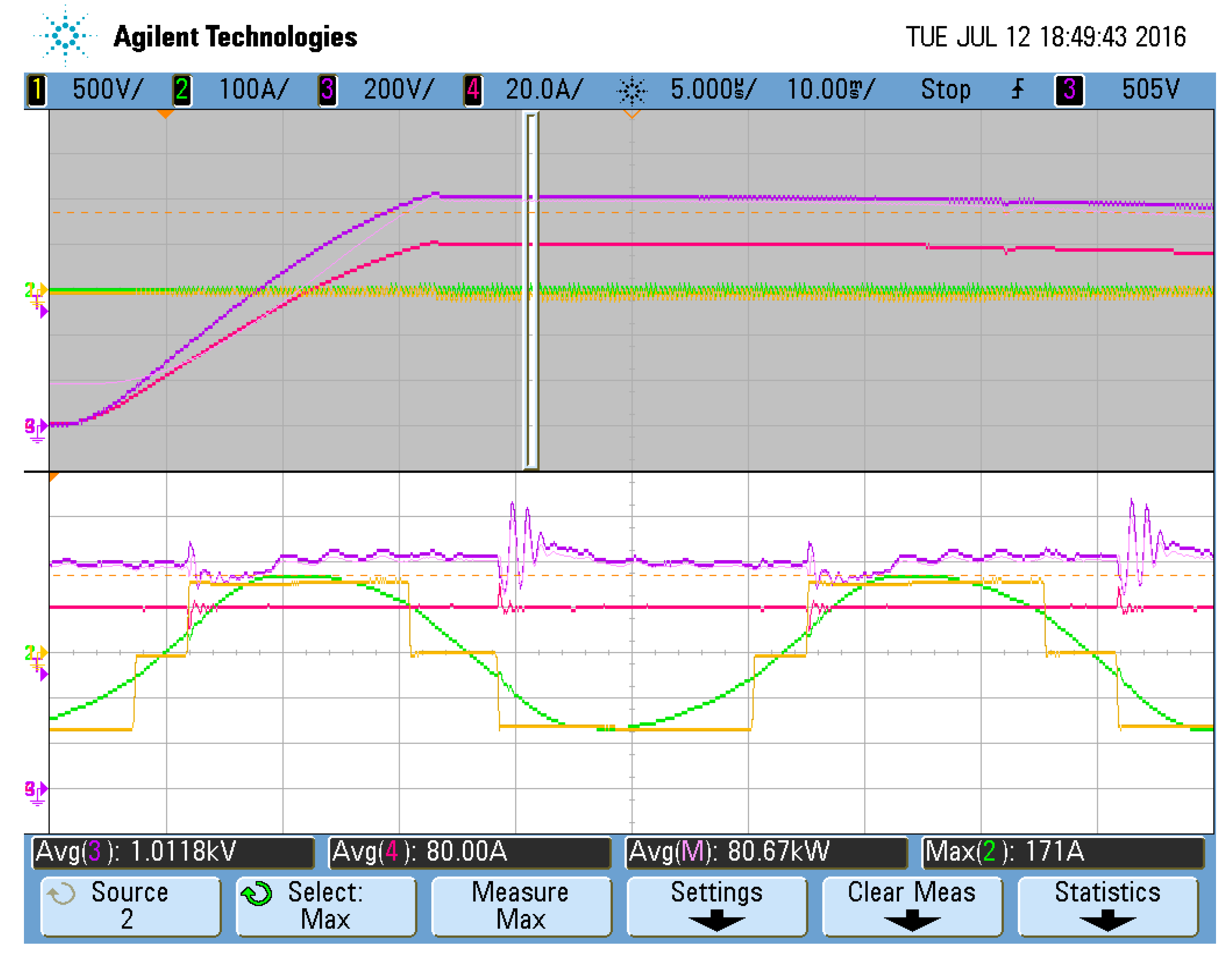
- VIN = 800 V, VO = 1000 V and PO = 80 kW (R = 12.5 Ω on the primary side and CO = 96 μF). Resonant current amplitude iPL = 171 A, duty cycle d = 0.358, switching frequency fS = 37.8 kHz.
In a first batch of tests, the 800 V–80 kW VIN input source was implemented by means of an electrolytic capacitor bank of 84 mF. The capacitor discharges from a maximum value (VIN = 825 V) to a minimum value (VIN = 720 V) as seen in Figure 12. The regulation works perfectly without appreciable overvoltage at the start-up.
3.1. Thermal Analisys
The losses in the experimental prototype are evaluated and compared with theoretical values. Measurements are taken on the case of the switches and on the heatsink near them. Additionally, the temperature profile, using both types of semiconductors, is analyzed with a thermal camera [37,38]. In this case, the mains are used as input voltage.
3.1.1. Thermal Analysis for PO = 5 kW
Thermal measurements of the converter for PO = 5 kW have been made under the following conditions:
- VIN = 300 V, VO = 255 V, PO = 5 kW.
- Si-IGBTs and SiC-MOSFETs as switches. Non-forced ventilation. Reference of the heatsink (Rthha = 0.063 °K/W) RG40160N87/500AFR.
The operating point of the converter, Figure 14, is in this case:
- Amplitude of the resonant current iPL = 43.8 A, switching current for leg (Q1–Q2) IS = 28.7 A, switching current for leg (Q3–Q4) IS = 38.7 A, switching frequency fS = 37.7 kHz and duty cycle d = 0.22.
Figure 15 and Figure 16 show the temperature increment vs. time. In these figures, AR01 represents the measurement area considered for leg Q3–Q4, AR02 is that associated to leg Q1–Q2, and AR03 is the heatsink. The temperatures measured after 15 min are shown in Table 2. It can be clearly observed how the temperature in the SiC MOSFETs is lower than that in the Si IGBTs.
It can also be observed that leg Q1–Q2, which experiences hard switching, is hotter than leg Q3–Q4, where ZVS takes place. As expected, it was not possible to complete the full power test with IGBTs: thermal problems made advisable not to go beyond 5 kW.
3.1.2. Thermal Analysis for PO = 20 kW
The thermal measurement of the converter for PO = 20 kW has been made under the following conditions:
- VIN = 400 V, VO = 500 V, PO = 20 kW
- SiC-MOSFETs. Non-forced ventilation. Reference of the heatsink (Rthha = 0.063 °K/W) RG40160N87/500AFR.
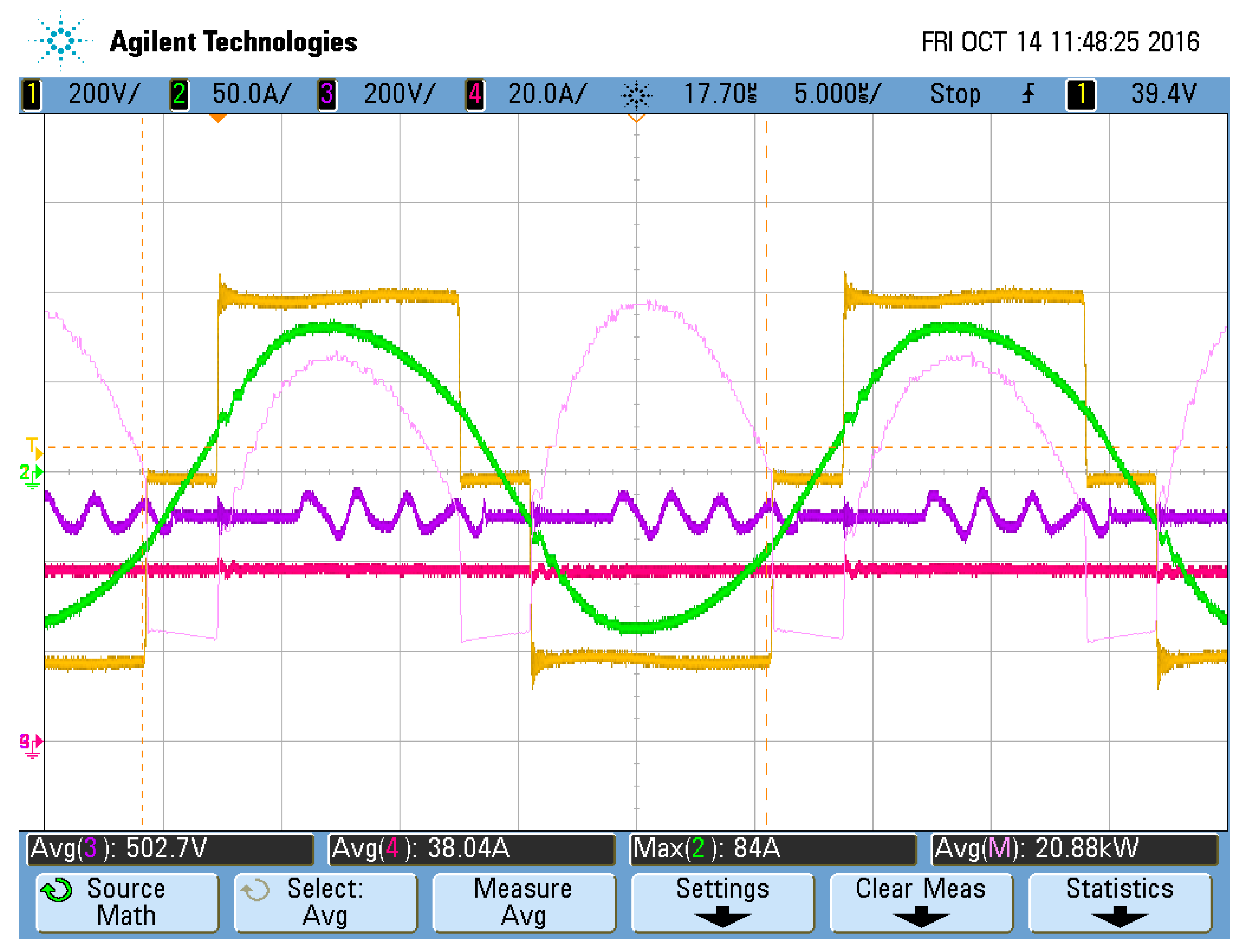
The operating point of the converter, Figure 17, in this case is:
- Amplitude of the resonant current iPL = 84 A, switching current for leg Q1–Q2 IS = 23 A, switching current for leg Q3–Q4 IS = 34 A, switching frequency fS = 37.7 kHz and duty cycle d = 0.385.
Figure 18 shows the temperature increment vs. time when the converter is assembled with SiC MOSFETs. AR01 represents the measurement area considered for leg Q3–Q4, AR02 is that associated to leg Q1–Q2, and AR03 is the heatsink. The temperatures measured after 15 min are shown in Table 3.
Table 4 shows that the temperature increment in the switches has been moderate. In fact, the dissipation in the semiconductors is mostly due to switching losses: they depend on the input voltage and the current value at the time of switching. Notice that, at 20 kW, the supply voltage is higher than the one corresponding to PO = 5 kW, whereas the switching current is lower; thus, overall increment of losses is far from being proportional to the delivered power.
3.1.3. Thermal Analysis to Estimate the Steady-State Temperature
Temperature variation in the converter has been measured using SiC MOSFET switches for a time interval of 3 h, so that it is possible to estimate the steady-state temperature value.
Thermal measurements of the converter for PO = 20 kW have been made under the following conditions:
- VIN = 400 V, VO = 500 V, PO = 20 kW
- SiC-MOSFETs. Non-forced ventilation. Reference of the heatsink (Rthha = 0.063 °K/W) RG40160N87/500AFR.
The operating point of the converter, Figure 17, in this case is:
- Amplitude of the resonant current iPL = 84 A, switching current for leg Q1–Q2 IS = 23 A, switching current for leg Q3–Q4 IS = 34 A, switching frequency fS = 37.7 kHz and duty cycle d = 0.385.
An exponential approximation has been used in order to estimate the temperature in the inverter’s steady state, since this state has not been reached during the measurement process (Figure 19). The maximum temperature for the semiconductors and the heatsink in steady state are: TQ1–Q2 = 65 °C, TQ3–Q4 = 60 °C and Th = 56 °C. In the case of the heatsink, the temperature rise is the result of the losses of the three-phase rectifier, the output rectifier and the inverter switches.
The temperature that would have reached the hottest element within each leg, Tj, has been calculated using Equations (16)–(18) and compared to that measured in the experimental results. The following values have been obtained: Tj(Q1,Q2) = 61.7 °C, Tj(Q3,Q4) = 58.9 °C and Th = 56.8 °C. These calculations are consistent with the experiments.
Tj(Q1,Q2) or Tj(Q3,Q4) are the temperatures at the junction of the switch, TH is the heatsink temperature and TA is the ambient temperature (all of them expressed in degrees Celsius). Rth values have been obtained from the datasheets, the power dissipated in one leg is PQ1–Q2; the one dissipated in one switch is P(Q1,Q2) that dissipated in the three-phase rectifier, PRecT; and the power loss in the output rectifier, PRecO. The expressions used for the calculations are (16)–(18):
The use of IGBTs is not recommended, since the temperatures reached by leg Q1–Q2 exceed 50 °C in only 15 min at 5 kW. On the other hand, temperature reaches only 40 °C at 20 kW with SIC MOSFET.
3.1.4. Power Loss Comparison
Table 5 shows a summary of the estimated power losses in the complete bridge for three different output powers, PO: 80 kW, 20 kW and 5 kW. In all the cases, efficiency close to 99% is achieved when using SiC MOSFET as switches.
3.2. High-Voltage Test
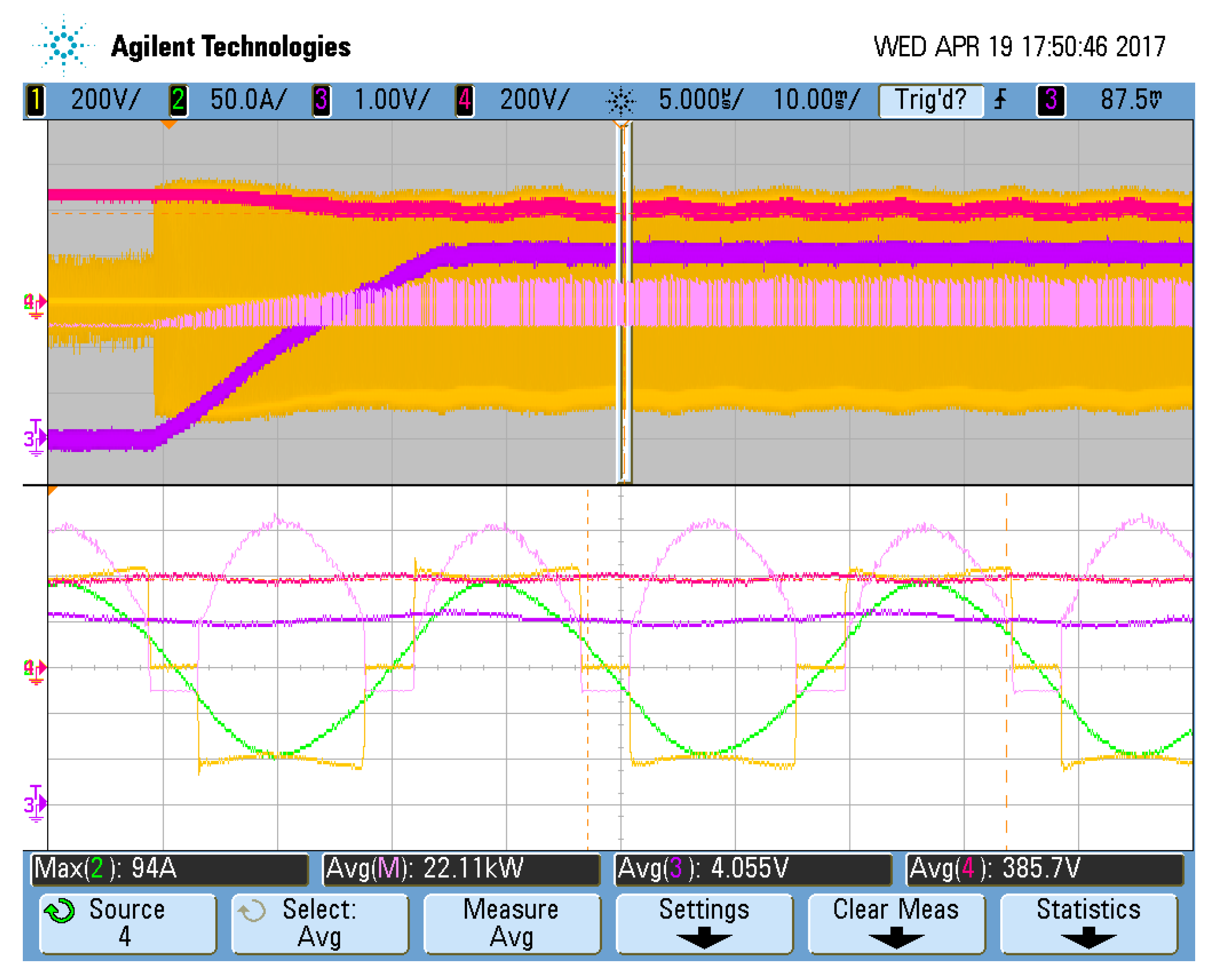
The authors tested in a previous work the inverter operating at low output voltage, without including the high-voltage transformer, and using analog control circuitry [33]. In the present work, the converter has been experimentally tested including the high-voltage transformer too [39,40,41], Figure 5. The results obtained allow a good operation of the converter to be verified, as shown in Figure 20. The original analog control circuitry has been replaced by a digital control circuit based on the TMS320F28027 microcontroller.
The operating point of the converter in Figure 20 is:
- VIN = 385 V, VO = 40.55 kV (1:10,000 ratio) and PO = 22.11 kW. Resonant current amplitude iPL = 94 A, duty cycle d = 0.43, switching frequency fS = 37.8 kHz.
4. Discussion
The study demonstrates that the use of SiC MOSFETs is an important improvement in high-power, high-voltage DC/DC converters for electrostatic precipitators. Lower switching losses (as compared to their IGBT-counterpart) lead to an efficiency in the prototype that is several points higher, both at high and low output power levels. Moreover, the switching characteristics of the MOSFETs influence the control strategy of the whole converter. With IGBTs, it was very important to ensure that the antiparallel diode was always ON before turning the main switch ON. However, with the new MOSFETs, preserving zero voltage switching is no longer so important. The mathematical models and the experimental measurements demonstrate that hard switching at 40 kHz is a good option. This gives rise to a new concept of “good behavior” in the inverter. The best way to reduce losses and current amplitude is to center the resonant current in the switching period, i.e., to make the phase between the current and the first harmonic of the inverter voltage zero. Instantaneous waveforms, thermal measurement and power balance in a full-scale prototype support the study with experimental evidence.
The control method has some limitations:
The converter is designed to operate at a constant frequency, therefore, it will be necessary to implement a variable frequency control to keep it in phase with the voltage when the load changes, controlling the mode centered in the current. The converter does not should to work with low duty cycles, since both legs would be switching with higher current values and thus will be increased the losses in the switches. This can occur for a constant load with low output voltages. A decrease in the load will produce an increase in the switching frequency to maintain the current in phase and, therefore, an increase in losses.
On the other hand, the architecture of the control has been digitally implemented. The small signal model of the topology is a good basis to support the design. A simple linear structure for the feedback is demonstrated to be valid. The transient response is fast enough, avoiding any overvoltage at the output. This is quite relevant, since, otherwise, the isolation in the step-up transformer could be under risk. Again, the experiments in the prototype verify the theoretical study, supporting the whole control scheme.
5. Conclusions
In this paper, a new centered-current control that allows reactive energy and, therefore, the current in the resonant tank to be minimized, thus reducing conduction losses, is proposed. Likewise, by means of this control mode, it is possible to reduce switching losses, since switching operations take place at low current. To improve the commutations, SiC MOSFETs have been used instead of Si IGBTs, which resulted in an efficiency of 98% in the power stage. A dynamic model has been proposed that allows a digital regulator to be calculated for a bandwidth of 500 Hz, typically enough for this type of application. This converter has been tested experimentally at nominal values and at high output voltage, with no appreciable over voltages having been observed with the selected regulator.
In order to complete the design of this converter it will be necessary to enhance the following goals in the future:
- Allow the digital control of the converter to adjust its frequency taking into account that the load R will be modified due to the conditions of the contaminated gases. Up to now, the constant R load has been considered.
- Implement a regulator that allows the rapid recovery of the output voltage in case of short-circuits, due to the effect of the back corona.
- Perform tests in the production plant where we have agreements with companies. In our case Arcelor-Mittal, a company dedicated to steel production in Asturias, Spain.
Acknowledgments
This work has been co-funded by the Plan of Science, Technology and Innovation of the Principality of Asturias through Project FC-15-GRUPIN14-122, and by the Spanish Government with the action TEC2014-53324-R.
Author Contributions
This paper is part of a research carried out by Pedro J. Villegas, and Juan A. Martín-Ramos, Juan Díaz and Juan Á. Martínez, whereas Miguel J. Prieto and Alberto M. Pernía assisted with thermal measurements and prototype development.
Conflicts of Interest
The authors declare no conflict of interest.
Abbreviations
| AR01 | Thermal measurement surface for Q3, Q3 leg |
| AR02 | Thermal measurement surface for Q1, Q2 leg |
| AR03 | Thermal measurement surface for heatsink |
| CP | Parasitic capacitance of the transformer |
| CS | Serial Capacitance of the topology |
| CX | Equivalent capacitor in large signal model |
| C(z) | Control (z) transference function |
| d | duty cycle |
| DA–DD | Output diodes |
| D1–D4 | Diodes in anti-parallel of switches |
| EOFF | Turn OFF Energy |
| EON | Turn ON energy |
| EREC | Diode Recovery Energy |
| ESP | Electrostatic Precipitators |
| G(s) | Power stage (s) transference function |
| G(z) | Power stage (z) transference function |
| fS | Switching frequency |
| H(z) | Feedback (z) transference function |
| HF-SMPS | High Frequency Switching Mode Power Supply |
| iD | Current through the output diodes |
| IGBT | Insulated Gate Bipolar Transistor |
| iPL | Current of the resonant tank |
| IAVG | Average current of the semiconductors |
| IN | Nominal Current of the switches (300 A on the datasheets) |
| IRMS | RMS current of the semiconductors |
| IS | Switching current |
| LS | Parasitic Inductance of the transformer |
| MOSFETs | Metal Oxide Semiconductor Field Effect Transistors |
| n1 and n2 | Numbers of turns in the primary, n1, and secondary, n2, of transformer |
| PO | Output power of the converter |
| P(Qx,Qy) | Power dissipated in each semiconductor |
| PQx–Qy | Power dissipated in one leg |
| PRecT | Power dissipated in tri-phase main power supply rectifier |
| PRecO | Power dissipated in output rectifier |
| PRC-LCC | Series-Parallel Resonant Converter with an inductive output filter |
| Q1–Q4 | Switches in the converter |
| R | Equivalent load of the converter |
| RCD | Conduction resistance of IGBT |
| RCESAT | Collector-Emitter saturation resistor |
| RD | Diode resistance |
| RDS | Drain-Source resistance |
| Rthch | Thermal resistance between case and heatsink |
| Rthha | Thermal resistance between heatsink and ambient |
| Rthjc | Thermal resistance between junction and case |
| RX | Equivalent resistor in large-signal model |
| r | Equivalent resistance of the circuit |
| t | Time |
| Si | Silicon |
| SiC | Silicon Carbide |
| T | Period |
| Tj | Junction Temperature |
| Th | Heatsink Temperature |
| TA | Ambient Temperature |
| VCESAT | Collector-Emitter saturation voltage |
| VD | Voltage drop in the semiconductors |
| VIN | Input DC voltage of the converter |
| VN | Nominal voltage of the switches (600 V on the datasheets) |
| VO | Output DC voltage of the converter |
| VAB | Input voltage of the resonant tank |
| VS | Voltage across the series inductance |
| VP | Voltage across the parallel capacitor, CP |
| ZCS | Zero-current switching |
| ZVS | Zero-voltage switching |
| ZOH | First order z conversion |
| ϕ | Delay between input voltage, VAB, and resonant current, iLP |
| Ψ | Output diodes clamping angle |
| ωs | Pulsating frequency |
References
- Chen, P.; Liu, Z.; Wun, M.; Kuo, T. Cellular Mutagenicity and Heavy Metal Concentrations of Leachates Extracted from the Fly and Bottom Ash Derived from Municipal Solid Waste Incineration. Int. J. Environ. Res. Public Health 2016, 13, 1078. [Google Scholar] [CrossRef] [PubMed]
- Reynolds, B.; Reddy, K.J.; Argyle, M.D. Field Application of Accelerated Mineral Carbonation. Minerals 2014, 4, 191–207. [Google Scholar] [CrossRef]
- Khalsa, J.H.A.; Döhling, F.; Berger, F. Foliage and Grass as Fuel Pellets–Small Scale Combustion of Washed and Mechanically Leached Biomass. Energies 2016, 9, 361. [Google Scholar] [CrossRef]
- Kim, B.; Han, O.; Jeon, H.; Baek, S.; Park, C. Trajectory Analysis of Copper and Glass Particles in Electrostatic Separation for the Recycling of ASR. Metals 2017, 7, 434. [Google Scholar] [CrossRef]
- Randstad, P. On High-Frequency Soft-Switching DC-Converters for High-Voltage Applications. Ph.D. Thesis, Royal Institute of Technology, Stockholm, Sweden, 2004. [Google Scholar]
- Grass, N.; Hartmann, W.; Klockner, M. Application of different types of high voltage supplies on industrial ESP. IEEE Trans. Ind. Appl. 2004, 40, 1513–1520. [Google Scholar] [CrossRef]
- Seitz, D.; Herder, H. Switch Mode Power Supplies for Electrostatic Precipitators. In Proceedings of the 8th International ICESP Conference, Birmingham, AL, USA, 14–17 May 2001. [Google Scholar]
- Reyes, V.; Lund, C.R. Full scale switch mode power supplies on an ESP at high resistivity operating conditions. In Proceedings of the 8th International ICESP Conference, Birmingham, AL, USA, 14–17 May 2001. [Google Scholar]
- Crynack, R. State-of-the-Art Electrostatic Precipitator Power Supplies; EPRI: Palo Alto, CA, USA, 2003. [Google Scholar]
- Vukosavić, S.N.; Perić, L.S.; Sušić, S.D. A Novel Power Converter Topology for Electrostatic Precipitators. IEEE Trans. Power Electron. 2016, 31, 152–164. [Google Scholar] [CrossRef]
- Zheng, S.; Czarkowski, D. High-voltage high-power resonant converter for electrostatic precipitator. In Proceedings of the Eighteenth Annual IEEE Applied Power Electronics Conference and Exposition APEC ’03, Miami Beach, FL, USA, 9–13 February 2003; Volume 2, pp. 1100–1104. [Google Scholar]
- Zhang, X.; Lai, Z.; Xiong, R.; Li, Z.; Zhang, Z.; Song, L. Switching Device Dead Time Optimization of Resonant Double-Sided LCC Wireless Charging System for Electric Vehicles. Energies 2017, 10, 1772. [Google Scholar] [CrossRef]
- Liu, X.; Clare, L.; Yuan, X.; Wang, C.; Liu, J. A Design Method for Making an LCC Compensation Two-Coil Wireless Power Transfer System More Energy Efficient Than an SS Counterpart. Energies 2017, 10, 1346. [Google Scholar] [CrossRef]
- Geng, Y.; Li, B.; Yang, Z.; Lin, F.; Sun, H. A High Efficiency Charging Strategy for a Supercapacitor Using a Wireless Power Transfer System Based on Inductor/Capacitor/Capacitor (LCC) Compensation Topology. Energies 2017, 10, 135. [Google Scholar] [CrossRef]
- Bhowmick, S.; Bhat, A.K.S. A fixed-frequency LCC-type resonant converter with inductive output filter using a modified gating scheme. In Proceedings of the 2014 International Conference on Advances in Energy Conversion Technologies (ICAECT), Manipal, India, 23–25 January 2014; pp. 140–145. [Google Scholar]
- Fang, Z.; Wang, J.; Duan, S.; Shao, J.; Hu, G. Stability Analysis and Trigger Control of LLC Resonant Converter for a Wide Operational Range. Energies 2017, 10, 1448. [Google Scholar] [CrossRef]
- Kou, B.; Zhang, H.; Zhang, H. A High-Precision Control for a ZVT PWM Soft-Switching Inverter to Eliminate the Dead-Time Effect. Energies 2016, 9, 579. [Google Scholar] [CrossRef]
- Hu, S.; Li, X.; Lu, M.; Luan, B. Operation Modes of a Secondary-Side Phase-Shifted Resonant Converter. Energies 2015, 8, 12314–12330. [Google Scholar] [CrossRef]
- Ranstad, P.; Nee, H.P. On the distribution of AC and DC winding capacitances in high frequency transformers with rectifier loads. IEEE Trans. Ind. Electron. 2011, 58, 1789–1798. [Google Scholar] [CrossRef]
- Johnson, S.D.; Witulsky, A.F.; Erickson, R.W. Comparison of resonant topologies in high voltage DC applications. IEEE Trans. Aerosp. Electron. Syst. 1988, 24, 263–274. [Google Scholar] [CrossRef]
- Bhat, A.K.S. Analysis and design of a series parallel resonant converter with capacitive output filter. IEEE Trans. Ind. Appl. 1991, 27, 523–530. [Google Scholar] [CrossRef]
- García, V.; Rico, M.; Sebastián, J.; Hernando, M.; Uceda, J. An optimized DC-DC converter topology for high voltage pulse loads applications. In Proceedings of the 25th Annual IEEE Power Electronics Specialists Conference, Taipei, Taiwan, 20–25 June 1994; pp. 1413–1421. [Google Scholar]
- Pernía, A.M.; Prieto, M.J.; Villegas, P.J.; Díaz, J.; Martín-Ramos, J.A. LCC Resonant Multilevel Converter for X-ray Applications. Energies 2017, 10, 1573. [Google Scholar] [CrossRef]
- Steigerwald, R.L. A comparison of half-bridge resonant converter topologies. IEEE Trans. Power Electron. 1988, 3, 174–182. [Google Scholar] [CrossRef]
- Martin-Ramos, J.; Pernía, A.M.; Diaz, J.; Nuño, F.; Martínez, J.A. Power supply for a high voltage application. IEEE Trans. Power Electron. 2008, 23, 1608–1619. [Google Scholar] [CrossRef]
- García, V.; Rico, M.; Sebastián, J.; Hernando, M. Using the hybrid series parallel resonant converter with capacitive output filter and PWM phase-shifted control for high-voltage applications. In Proceedings of the 20th International Conference on Industrial Electronics, Control and Instrumentation, Bologna, Italy, 5–9 September 1994; pp. 1659–1664. [Google Scholar]
- Iannello, C.; Luo, S.; Batarseh, I. Full bridge ZCS PWM converter for high-voltage high-power applications. IEEE Trans. Aerosp. Electron. Syst. 2002, 38, 515–526. [Google Scholar] [CrossRef]
- Loef, C. Analysis of a full bridge LCC-type parallel resonant converter with capacitive output filter. In Proceedings of the 28th Annual IEEE Power Electronics Specialists Conference, Saint Louis, MO, USA, 27 June 1997; pp. 1402–1407. [Google Scholar]
- Ivensky, G.; Kats, A.; Ben-Yaakov, S. An RC load model of parallel and series parallel DC-DC converters with capacitive output filter. IEEE Trans. Power Electron. 1999, 14, 515–521. [Google Scholar] [CrossRef]
- Martin-Ramos, J.; Diaz, J.; Pernía, A.M.; Lopera, J.M.; Nuño, F. Dynamic and steady state models for the PRC-LCC topology with a capacitor as output filter. IEEE Trans. Ind. Electron. 2007, 54, 2262–2275. [Google Scholar] [CrossRef]
- Yang, R.; Ding, H.; Xu, Y.; Yao, L.; Xiang, Y. An analytical steady state model of LCC type series-parallel resonant converter with capacitive output filter. IEEE Trans. Power Electron. 2014, 29, 328–338. [Google Scholar] [CrossRef]
- Li, H.; Li, X.; Lu, M.; Hu, S. A Linearized Large Signal Model of an LCL-Type Resonant Converter. Energies 2015, 8, 1848–1864. [Google Scholar] [CrossRef]
- Villegas, P.J.; Ramos, J.A.M.; González, J.D.; Esteban, A.J.M. A Power Converter for an Electrostatic Precipitator using SiC MOSFETs. In Proceedings of the 9th Annual IEEE Energy Conversion Congress & Exposition (ECCE 2017), Cincinnati, OH, USA, 1–5 October 2017; pp. 4144–4151. [Google Scholar]
- Alvarez-Alvarez, A.; Mayor, H.A.; Villegas, P.J.; Pernía, A.M.; Nuño, F.; Martín-Ramos, J.A. Experimental measurement of power supplies dynamic behavior. In Proceedings of the 42nd Annual Conference of the IEEE Industrial Electronics Society, Florence, Italy, 23–26 October 2016; pp. 1–7. [Google Scholar]
- Meng, Z.; Wang, Y.; Yang, L.; Li, W. High Frequency Dual-Buck Full-Bridge Inverter Utilizing a Dual-Core MCU and Parallel Algorithm for Renewable Energy Applications. Energies 2017, 10, 402. [Google Scholar] [CrossRef]
- Reverter, F. The Art of Directly Interfacing Sensors to Microcontrollers. J. Low Power Electron. Appl. 2012, 2, 265–281. [Google Scholar] [CrossRef]
- Salamone, F.; Danza, L.; Meroni, I.; Pollastro, M.C. A Low-Cost Environmental Monitoring System: How to Prevent Systematic Errors in the Design Phase through the Combined Use of Additive Manufacturing and Thermographic Techniques. Sensors 2017, 17, 828. [Google Scholar] [CrossRef] [PubMed]
- Hammami, M.; Torretti, S.; Grimaccia, F.; Grandi, G. Thermal and Performance Analysis of a Photovoltaic Module with an Integrated Energy Storage System. Appl. Sci. 2017, 7, 1107. [Google Scholar] [CrossRef]
- Lv, Y.; Rafiq, M.; Li, C.; Shan, B. Study of Dielectric Breakdown Performance of Transformer Oil Based Magnetic Nanofluids. Energies 2017, 10, 1025. [Google Scholar] [CrossRef]
- Huang, P.; Mao, C.; Wang, D. Electric Field Simulations and Analysis for High Voltage High Power Medium Frequency Transformer. Energies 2017, 10, 371. [Google Scholar] [CrossRef]
- Tenbohlen, S.; Coenen, S.; Djamali, M.; Müller, A.; Samimi, M.H.; Siegel, M. Diagnostic Measurements for Power Transformers. Energies 2016, 9, 347. [Google Scholar] [CrossRef]
Figure 1.
Series–parallel resonant topology, PRC-LCC, with a capacitor as output filter.

Figure 2.
Waveforms for (a) Optimum switching control and (b) Centered-current control.


Figure 3.
Equivalent circuit of the topology according to [25,33]. Waveforms are expressed as amplitudes.

Figure 4.
Main waveforms of the topology. VAB is the input voltage of the resonant tank. iLP is the current of the resonant tank. VS is the voltage of the series inductance. VP is the voltage of the parallel capacitor CP. iD is the current through the output diodes. ϕ is the delay between input voltage VAB and resonant current iLP.

Figure 5.
High-voltage transformer (b) and simplified equivalent circuit (a) of the step-up transformer.
Figure 5.
High-voltage transformer (b) and simplified equivalent circuit (a) of the step-up transformer.

Figure 6.
(a) Initially Q1 is ON and Q2 is OFF. In this case, Q1 is ON but current flows through D1; (b) during switching, Q1 switches OFF before Q2 switches ON. C1 and C2 continue to have 0 V and VIN respectively across their terminals. When Q2 is turned ON, diode D1 will be forced OFF, C1 will be charged up to VIN and C2 will be fully discharged.

Figure 7.
This figure shows the switching process for leg Q3–Q4. (a) Initially Q3 is ON and Q4 is OFF; In this case (b), Q4 switches ON with zero voltage, because the diode in parallel D4 is conducting. Thus, no turn-on losses are expected in Q4. However, they appear during the OFF transition of Q3.

Figure 8.
(a) Theoretical waveforms of VAB (red) and iPL (blue); (b) Experimental waveforms of VAB (yellow) and iPL (green) scaled to VIN = 80 V, VO = 100 V and PO = 800 W.
Figure 8.
(a) Theoretical waveforms of VAB (red) and iPL (blue); (b) Experimental waveforms of VAB (yellow) and iPL (green) scaled to VIN = 80 V, VO = 100 V and PO = 800 W.

Figure 9.
Experimental (orange) and theoretical (blue) Bode plots for the power source operating on scaled output voltage and power using centered-current control. (a) Magnitude in (dB) and (b) phase in degrees.
Figure 9.
Experimental (orange) and theoretical (blue) Bode plots for the power source operating on scaled output voltage and power using centered-current control. (a) Magnitude in (dB) and (b) phase in degrees.
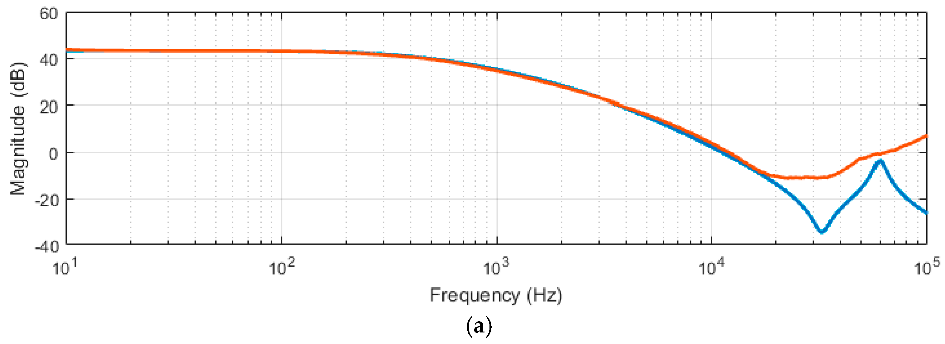
Figure 10.
Experimental converter used to obtain the Bode diagram and the corresponding waveforms. The transformer has been replaced by discrete LS and CP parts.
Figure 10.
Experimental converter used to obtain the Bode diagram and the corresponding waveforms. The transformer has been replaced by discrete LS and CP parts.

Figure 11.
Digital Feedback system block diagram.

Figure 12.
Experimental waveforms. VAB (yellow), iPL (green), VO (magenta). Bottom: Zoom of the top waveform.
Figure 12.
Experimental waveforms. VAB (yellow), iPL (green), VO (magenta). Bottom: Zoom of the top waveform.

Figure 13.
Converter Test Bench with digital control.
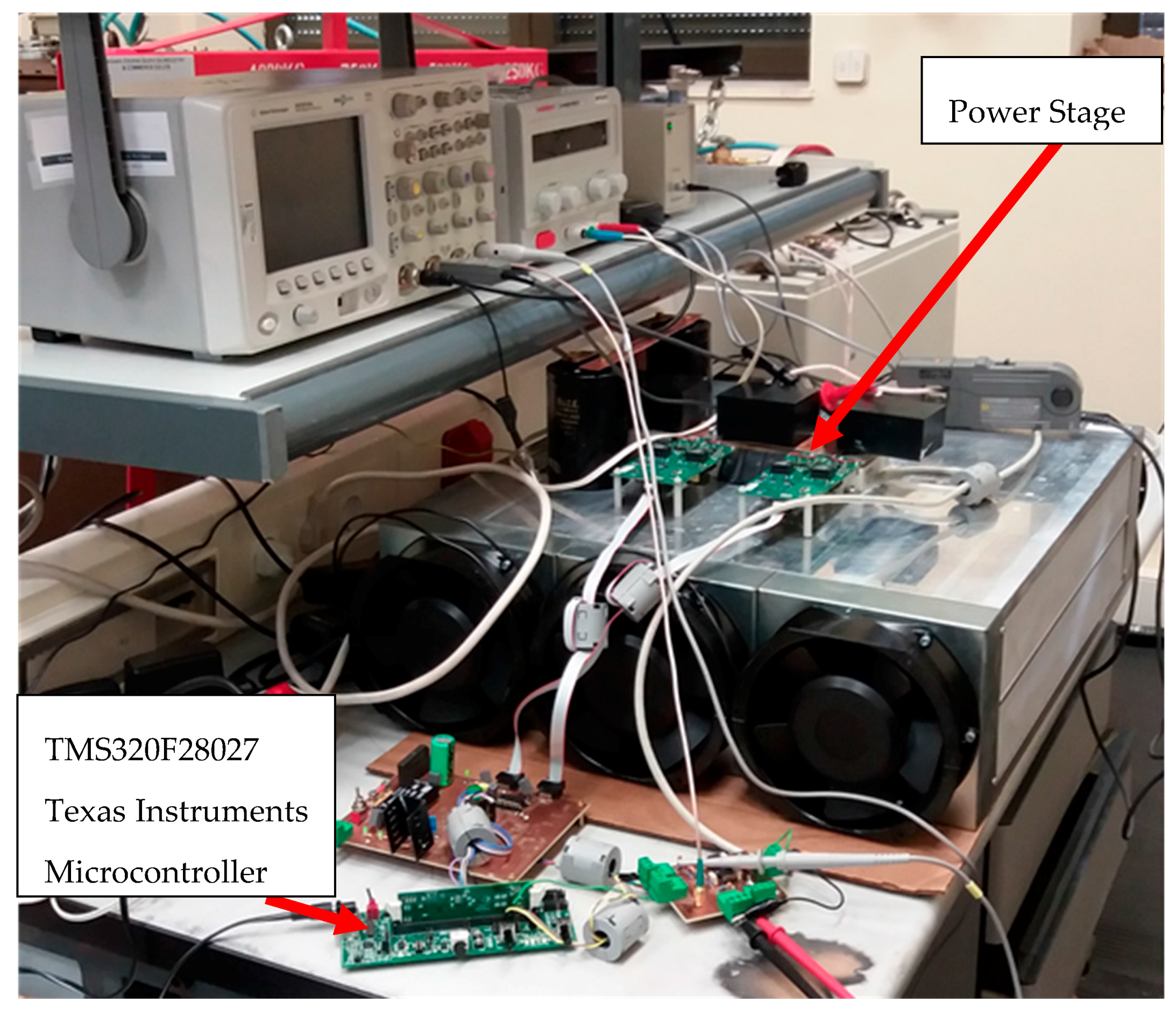
Figure 14.
Experimental waveforms for VAB (yellow) and iPL (green), with Vin = 300 V, VO = 250 V and PO = 5 kW.
Figure 14.
Experimental waveforms for VAB (yellow) and iPL (green), with Vin = 300 V, VO = 250 V and PO = 5 kW.
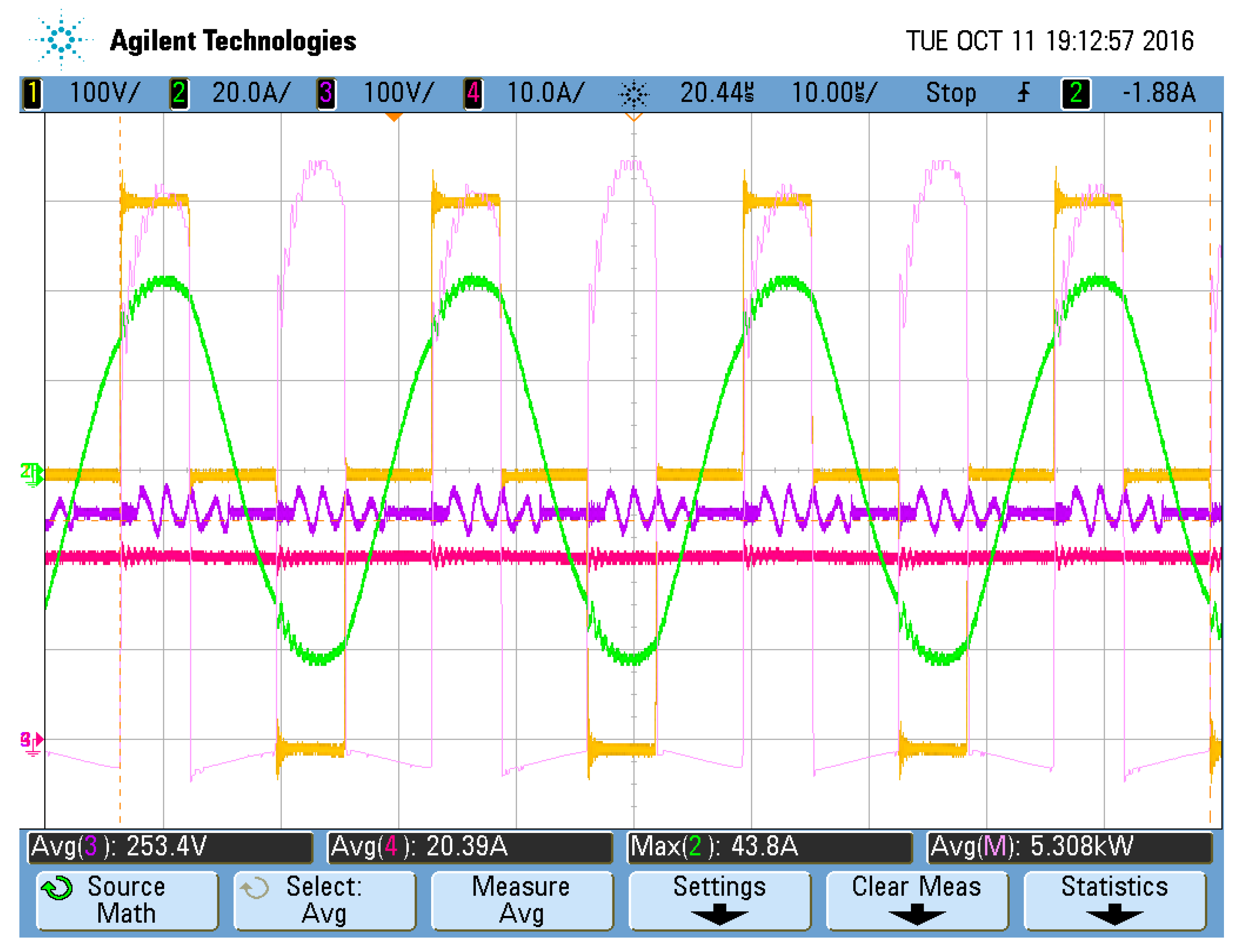
Figure 15.
Temperature Measurement (5 kW) of each leg using IGBTs FF300R12KS4. (a) Infrared image of power stage; (b) Maximum, minimum and difference values measured in each AR0x zone; (c) Temperature evolution in each leg and heatsink; blue: AR02 (Q1–Q2); red: AR01 (Q3–Q4); green: AR03 (heatsink).
Figure 15.
Temperature Measurement (5 kW) of each leg using IGBTs FF300R12KS4. (a) Infrared image of power stage; (b) Maximum, minimum and difference values measured in each AR0x zone; (c) Temperature evolution in each leg and heatsink; blue: AR02 (Q1–Q2); red: AR01 (Q3–Q4); green: AR03 (heatsink).
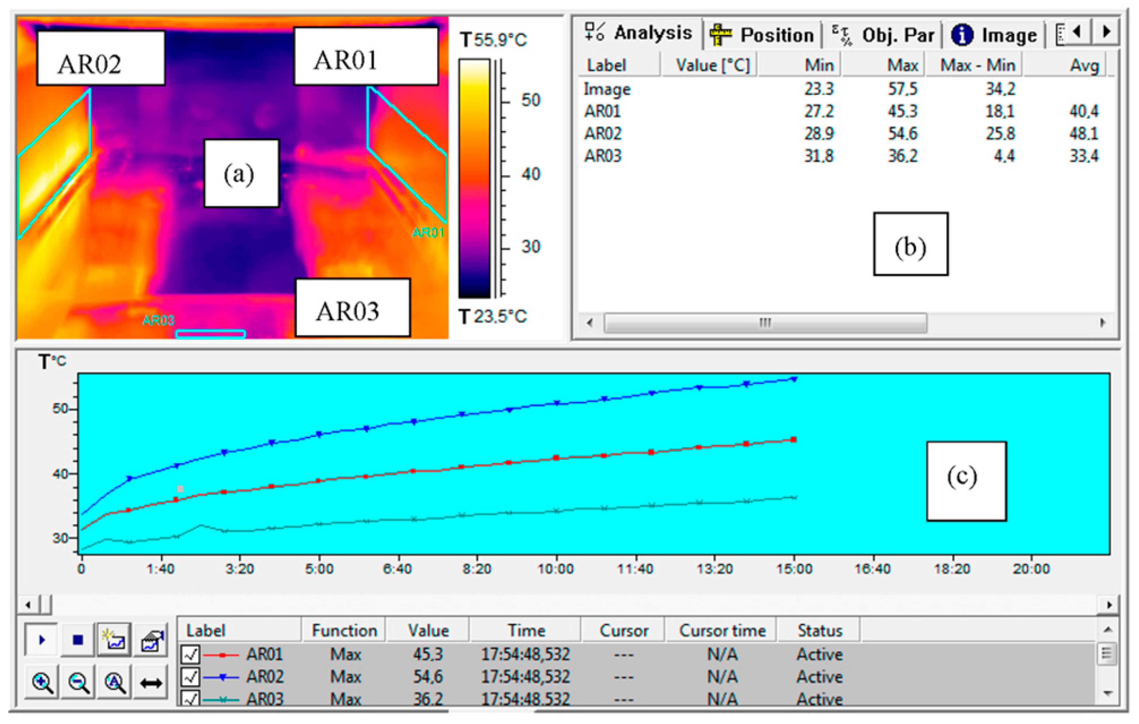
Figure 16.
Temperature Measurement (5 kW) of each leg using MOSFETs CAS300M12BM2. (a) Infrared image of power stage; (b) Maximum, minimum and difference values measured in each AR0x zone; (c) Temperature evolution in each leg and heatsink; blue: AR02 (Q1–Q2); red: AR01 (Q3–Q4); green: AR03 (heatsink).
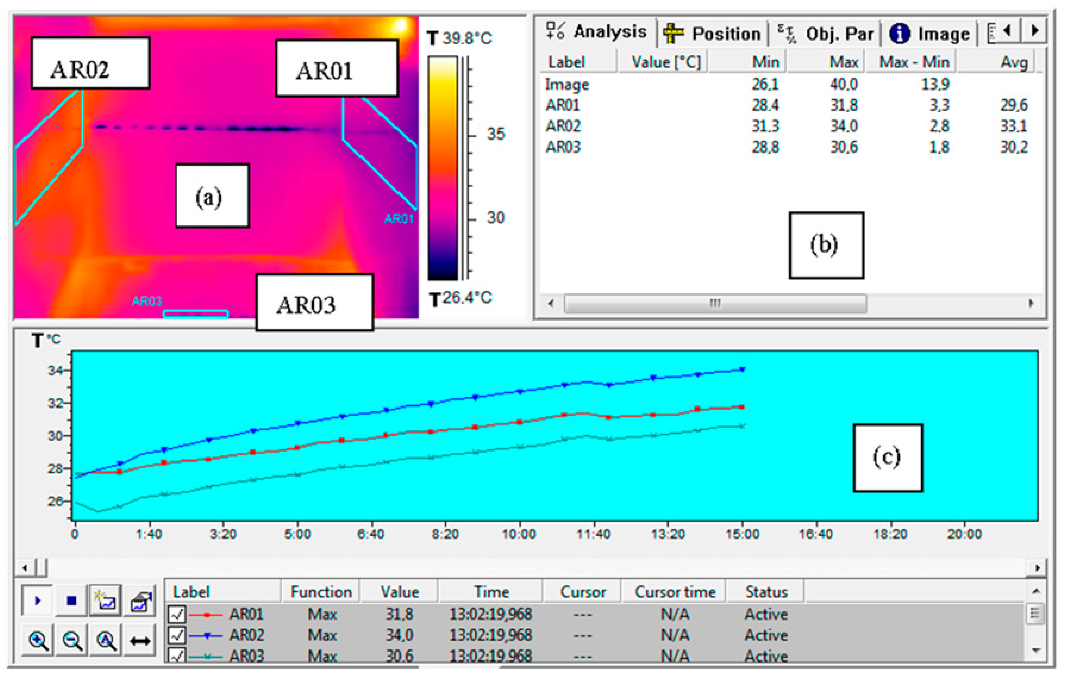
Figure 17.
Experimental waveforms for VAB (yellow) and iPL (green), with Vin = 400 V, VO = 500 V and PO = 20 kW.
Figure 17.
Experimental waveforms for VAB (yellow) and iPL (green), with Vin = 400 V, VO = 500 V and PO = 20 kW.

Figure 18.
Temperature Measurement (20 kW) of each leg using MOSFETs CAS300M12BM2. (a) Infrared image of power stage; (b) Maximum, minimum and difference values measured in each AR0x zone; (c) Temperature evolution in each leg and heatsink; blue: AR02 (Q1–Q2); red: AR01 (Q3–Q4); green: AR03 (heatsink).
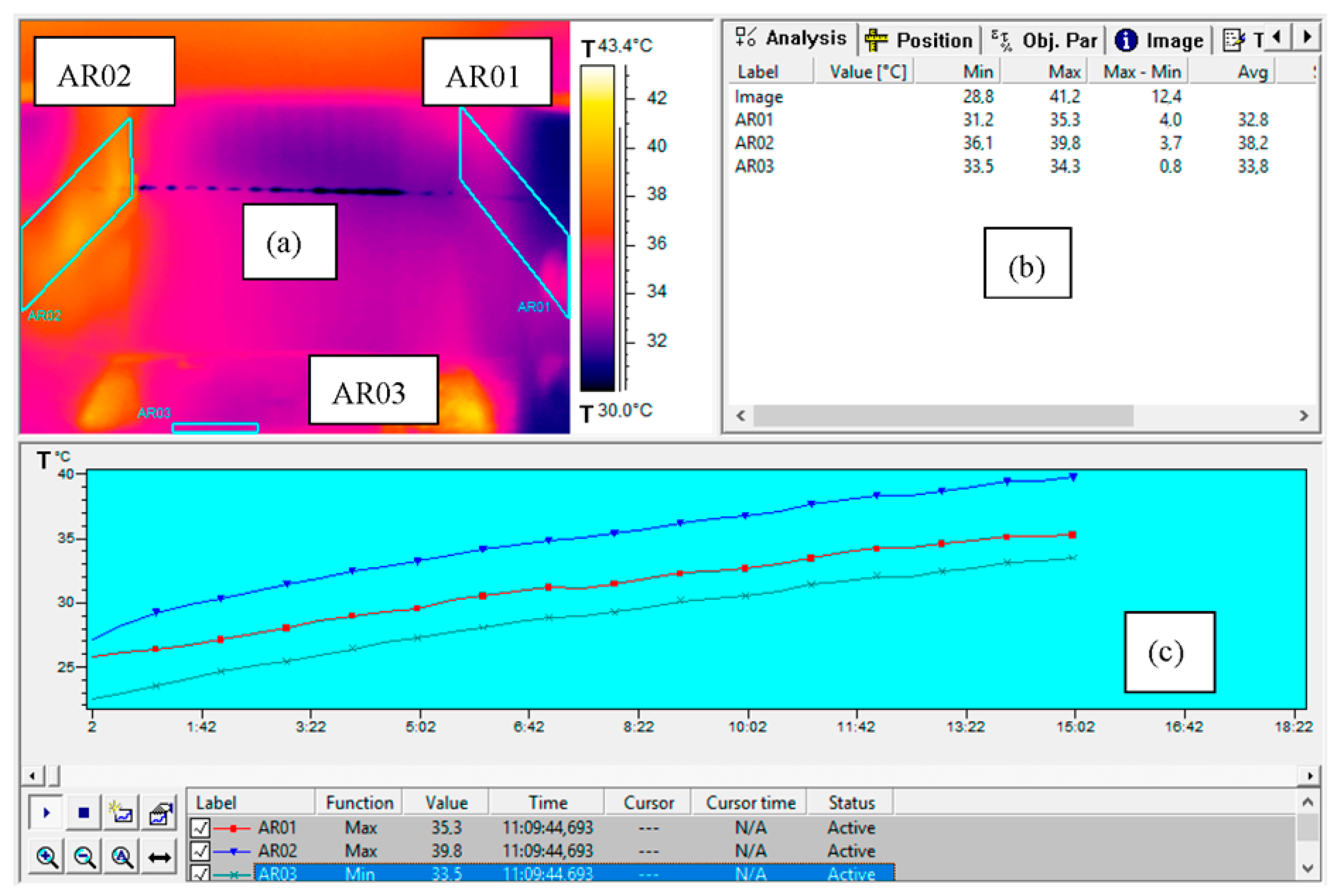
Figure 19.
Measurement of temperature in °C (20 kW) for each leg and for the heatsink using MOSFET CAS300M12BM2 for a time interval of 3 h (dots). Exponential approximations are also included for the temperature (a) in Q3–Q4 (blue), (b) Q1–Q2 (red) and (c) heatsink (green).
Figure 19.
Measurement of temperature in °C (20 kW) for each leg and for the heatsink using MOSFET CAS300M12BM2 for a time interval of 3 h (dots). Exponential approximations are also included for the temperature (a) in Q3–Q4 (blue), (b) Q1–Q2 (red) and (c) heatsink (green).
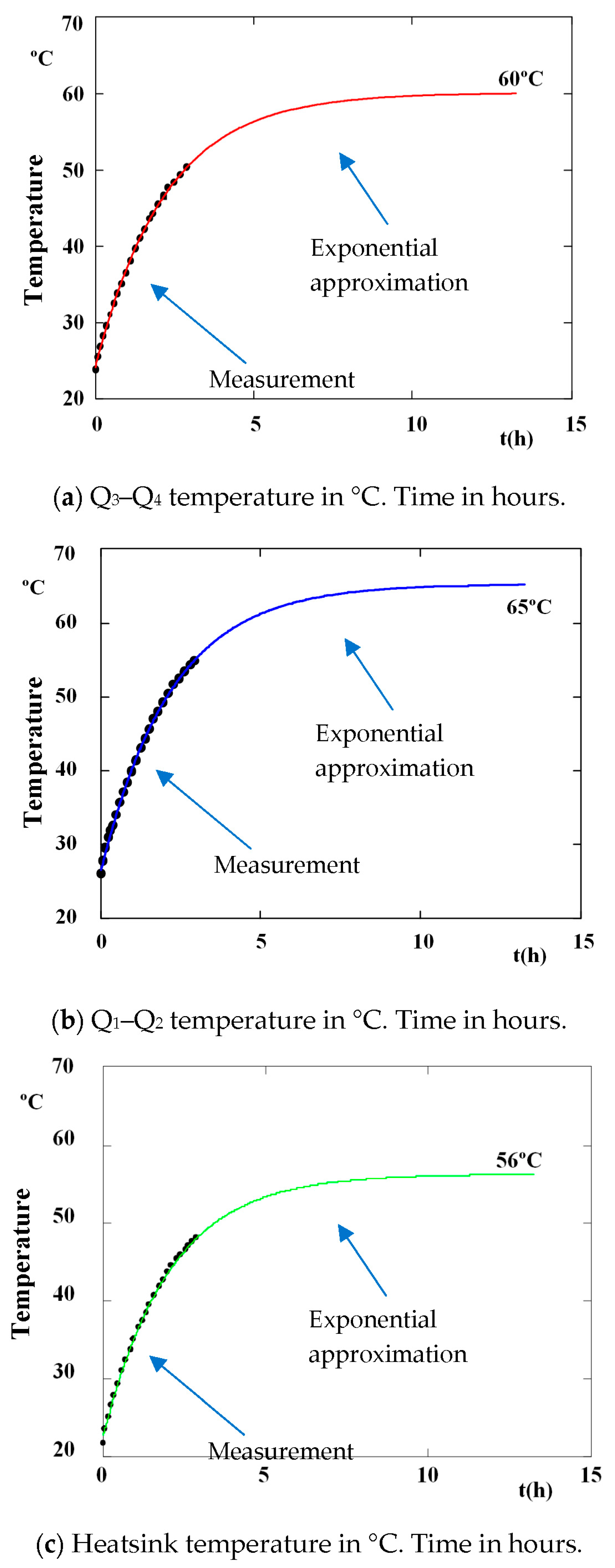
Figure 20.
Experimental waveforms for VAB (yellow) and iPL (green), with VIN = 385 V (red), VO = 40 kV (magenta) and PO = 22 kW.
Figure 20.
Experimental waveforms for VAB (yellow) and iPL (green), with VIN = 385 V (red), VO = 40 kV (magenta) and PO = 22 kW.


Table 1.
Power Dissipation in a Full Bridge at nominal conditions. POUT = 80 kW, VIN = 800 V, VO = 1000 V.
Table 1.
Power Dissipation in a Full Bridge at nominal conditions. POUT = 80 kW, VIN = 800 V, VO = 1000 V.
| POUT = 80 kW VIN = 800 V VO = 1000 V | ||||
|---|---|---|---|---|
| Power | Q1–Q2 | Q3–Q4 | Total | ηFB |
| IGBT | 1.71 kW | 836 W | 2.547 kW | 96.9% |
| MOSFET | 503 W | 237 W | 740 W | 99% |
Table 2.
Temperature Measurements for PO = 5 kW in SiC MOSFET and Si IGBT after 15 min.
| PO = 5 kW VIN = 300 V VO = 250 V | |||
|---|---|---|---|
| Temperature | TQ1–Q2 | TQ3–Q4 | THeatsink |
| IGBT | 54.6 °C | 45.3 °C | 36.2 °C |
| MOSFET | 34 °C | 31.8 °C | 30.6 °C |
Table 3.
Temperature Measurements for PO = 20 kW in SiC MOSFET after 15 min.
| PO = 20 kW VIN = 400 V VO = 500 V | |||
|---|---|---|---|
| Temperature | TQ1–Q2 | TQ3–Q4 | THeatsink |
| MOSFET | 39.9 °C | 35.3 °C | 34.3 °C |
Table 4.
Temperature Measurements for SiC MOSFET and Si IGBT after 15 min for 5 kW and 20 kW.
| POUT = 20 kW VIN = 400 V VO = 500 V | |||
| Temperature | TQ1–Q2 | TQ3–Q4 | THeatsink |
| MOSFET | 39.9 °C | 35.3 °C | 34.3 °C |
| POUT = 5 kW VIN = 300 V VO = 250 V | |||
| IGBT | 54.6 °C | 45.3 °C | 36.2 °C |
| MOSFET | 34 °C | 31.8 °C | 30.6 °C |
Summary of the temperatures reached by the switches and heatsinks for the indicated operating points after 15 min and for the switches used.
Table 5.
Theoretical Power Dissipation in Full Bridge topology.
| POUT = 80 kW VIN = 800 V VO = 1000 V | ||||
| Power | Q1–Q2 | Q3–Q4 | Total | ηFB |
| IGBT | 1.71 kW | 836 W | 2.547 kW | 96.9% |
| MOSFET | 503 W | 237 W | 740 W | 99% |
| POUT = 20 kW VIN = 400 V VO = 500 V | ||||
| IGBT | 515 W | 239 W | 755 W | 96.3% |
| MOSFET | 107 W | 47 W | 154 W | 99.2% |
| POUT = 5 kW VIN = 300 V VO = 250 V | ||||
| IGBT | 407 W | 166 W | 573 W | 89.7% |
| MOSFET | 70 W | 28 W | 98 W | 98% |
© 2017 by the authors. Licensee MDPI, Basel, Switzerland. This article is an open access article distributed under the terms and conditions of the Creative Commons Attribution (CC BY) license (http://creativecommons.org/licenses/by/4.0/).
Share and Cite
MDPI and ACS Style
Villegas, P.J.; Martín-Ramos, J.A.; Díaz, J.; Martínez, J.Á.; Prieto, M.J.; Pernía, A.M. A Digitally Controlled Power Converter for an Electrostatic Precipitator. Energies 2017, 10, 2150. https://doi.org/10.3390/en10122150
AMA Style
Villegas PJ, Martín-Ramos JA, Díaz J, Martínez JÁ, Prieto MJ, Pernía AM. A Digitally Controlled Power Converter for an Electrostatic Precipitator. Energies. 2017; 10(12):2150. https://doi.org/10.3390/en10122150
Chicago/Turabian StyleVillegas, Pedro J., Juan A. Martín-Ramos, Juan Díaz, Juan Á. Martínez, Miguel J. Prieto, and Alberto M. Pernía. 2017. "A Digitally Controlled Power Converter for an Electrostatic Precipitator" Energies 10, no. 12: 2150. https://doi.org/10.3390/en10122150
Note that from the first issue of 2016, this journal uses article numbers instead of page numbers. See further details here.