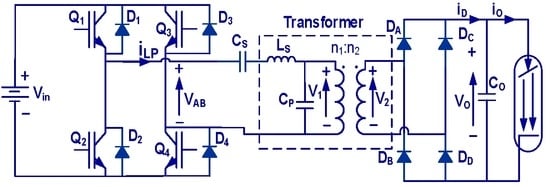
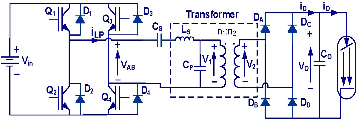
Figure 1.
Series–parallel resonant topology, PRC-LCC, with a capacitor as output filter.
Figure 1.
Series–parallel resonant topology, PRC-LCC, with a capacitor as output filter.
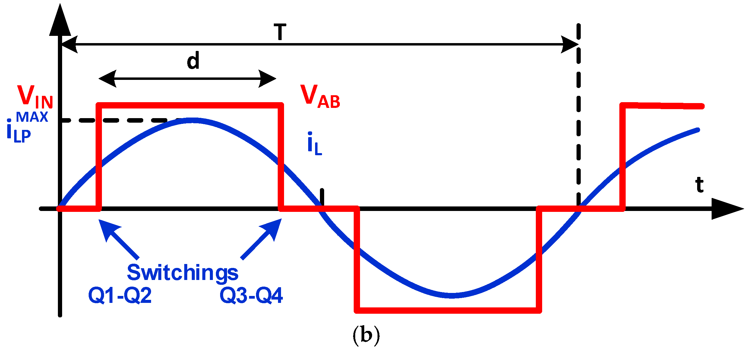
Figure 2.
Waveforms for (a) Optimum switching control and (b) Centered-current control.
Figure 2.
Waveforms for (a) Optimum switching control and (b) Centered-current control.
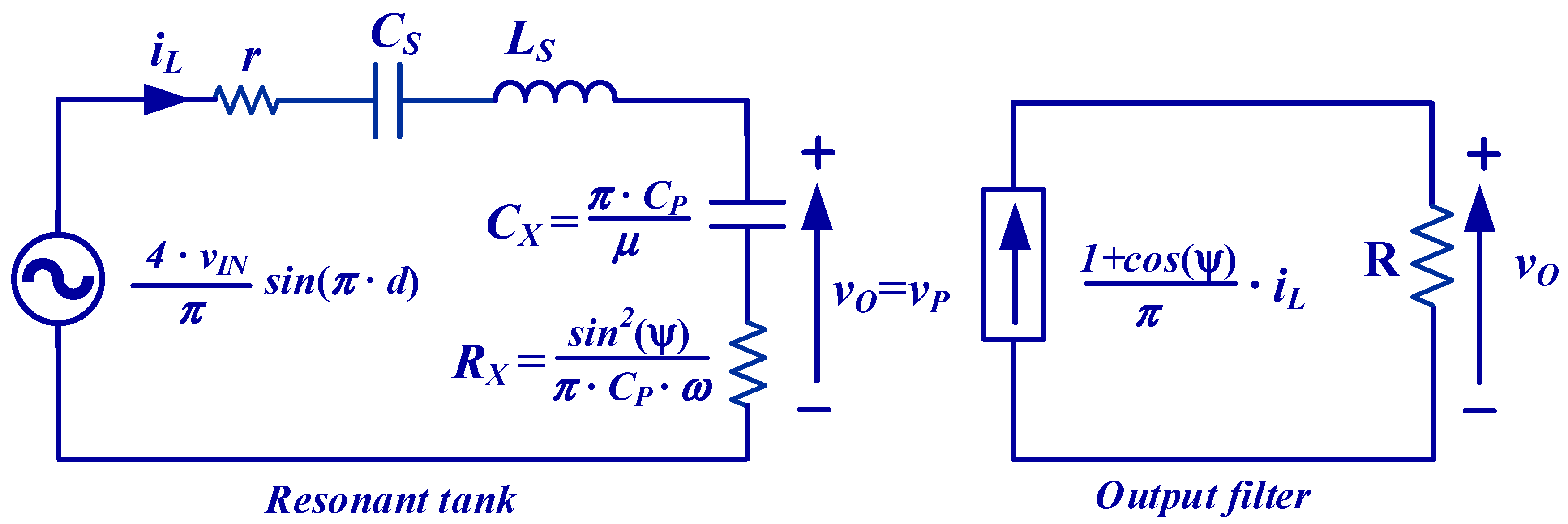
Figure 3.
Equivalent circuit of the topology according to [
25,
33]. Waveforms are expressed as amplitudes.
Figure 3.
Equivalent circuit of the topology according to [
25,
33]. Waveforms are expressed as amplitudes.
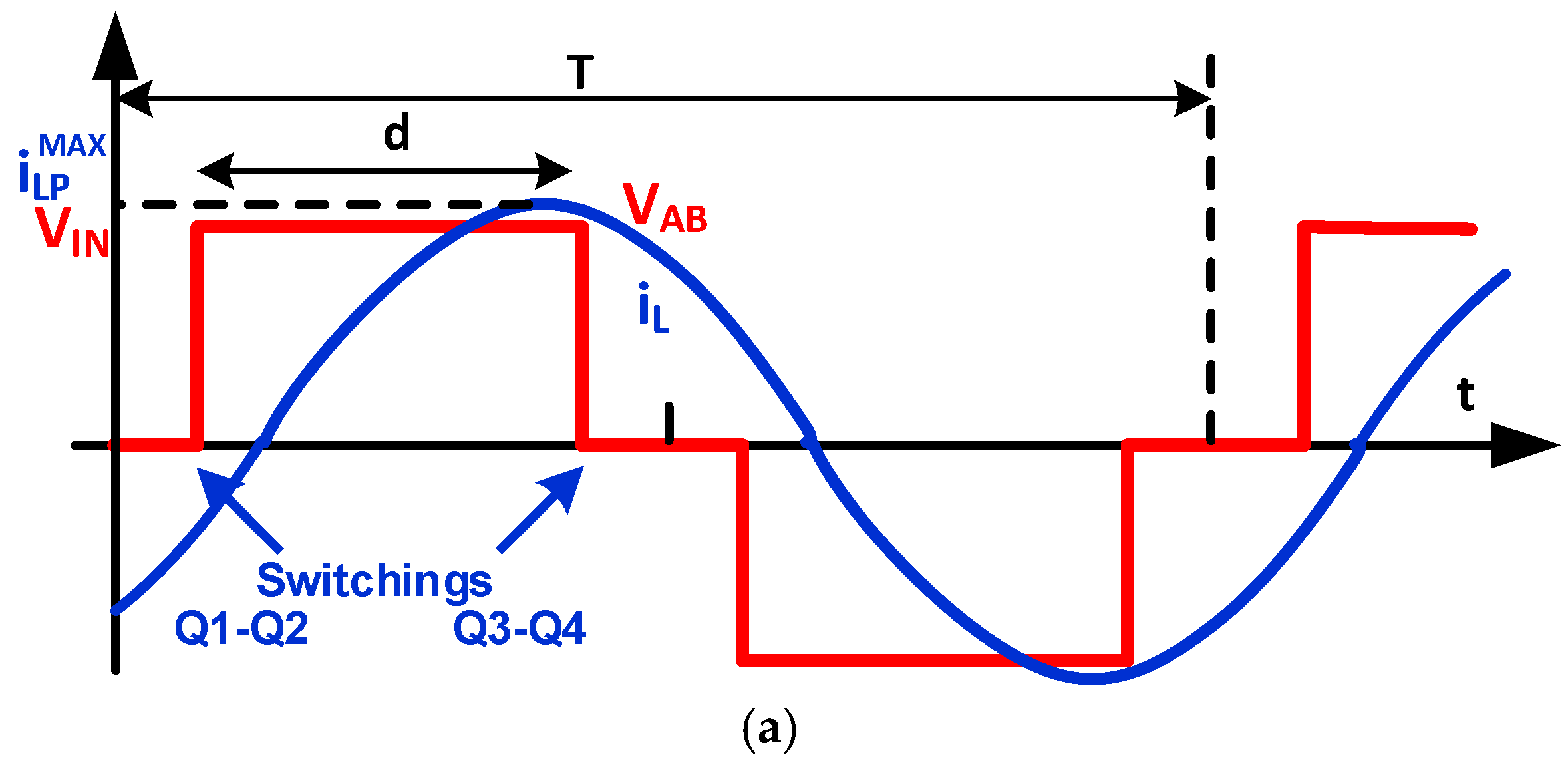
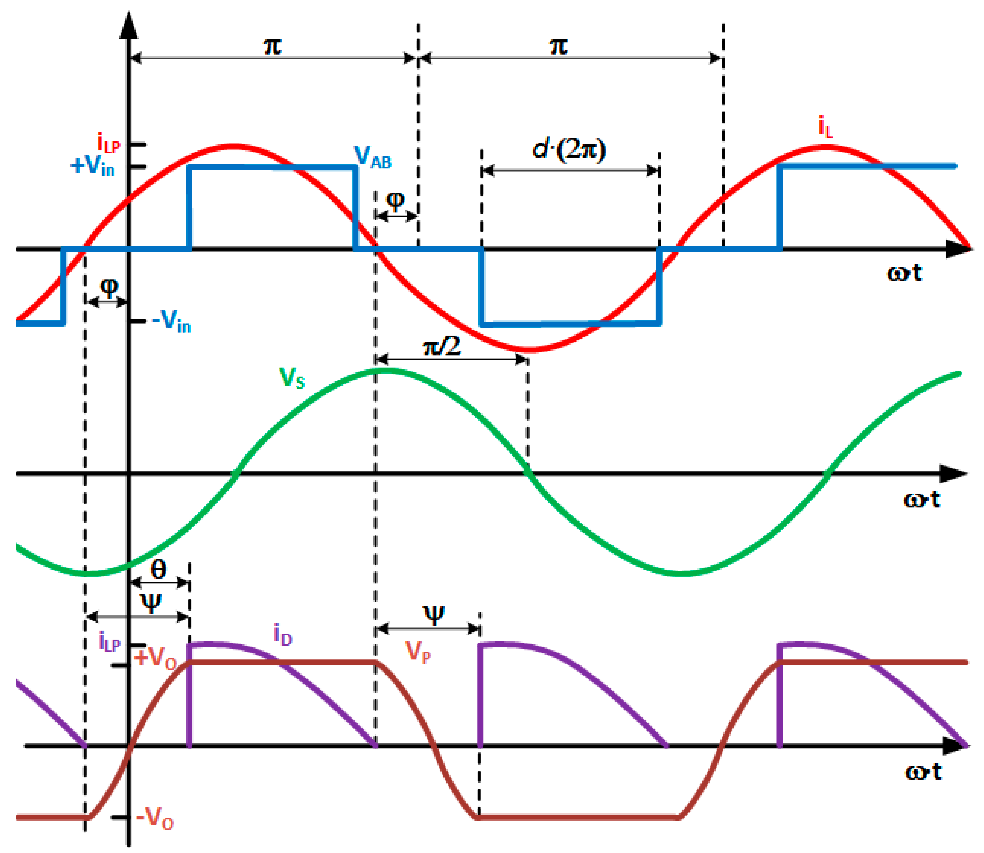
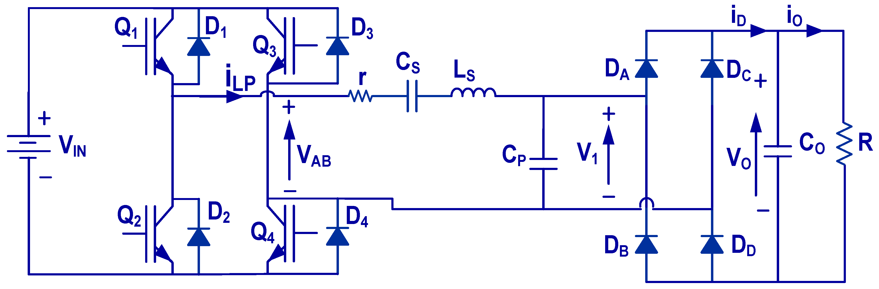
Figure 4.
Main waveforms of the topology. VAB is the input voltage of the resonant tank. iLP is the current of the resonant tank. VS is the voltage of the series inductance. VP is the voltage of the parallel capacitor CP. iD is the current through the output diodes. ϕ is the delay between input voltage VAB and resonant current iLP.
Figure 5.
High-voltage transformer (b) and simplified equivalent circuit (a) of the step-up transformer.
Figure 5.
High-voltage transformer (b) and simplified equivalent circuit (a) of the step-up transformer.
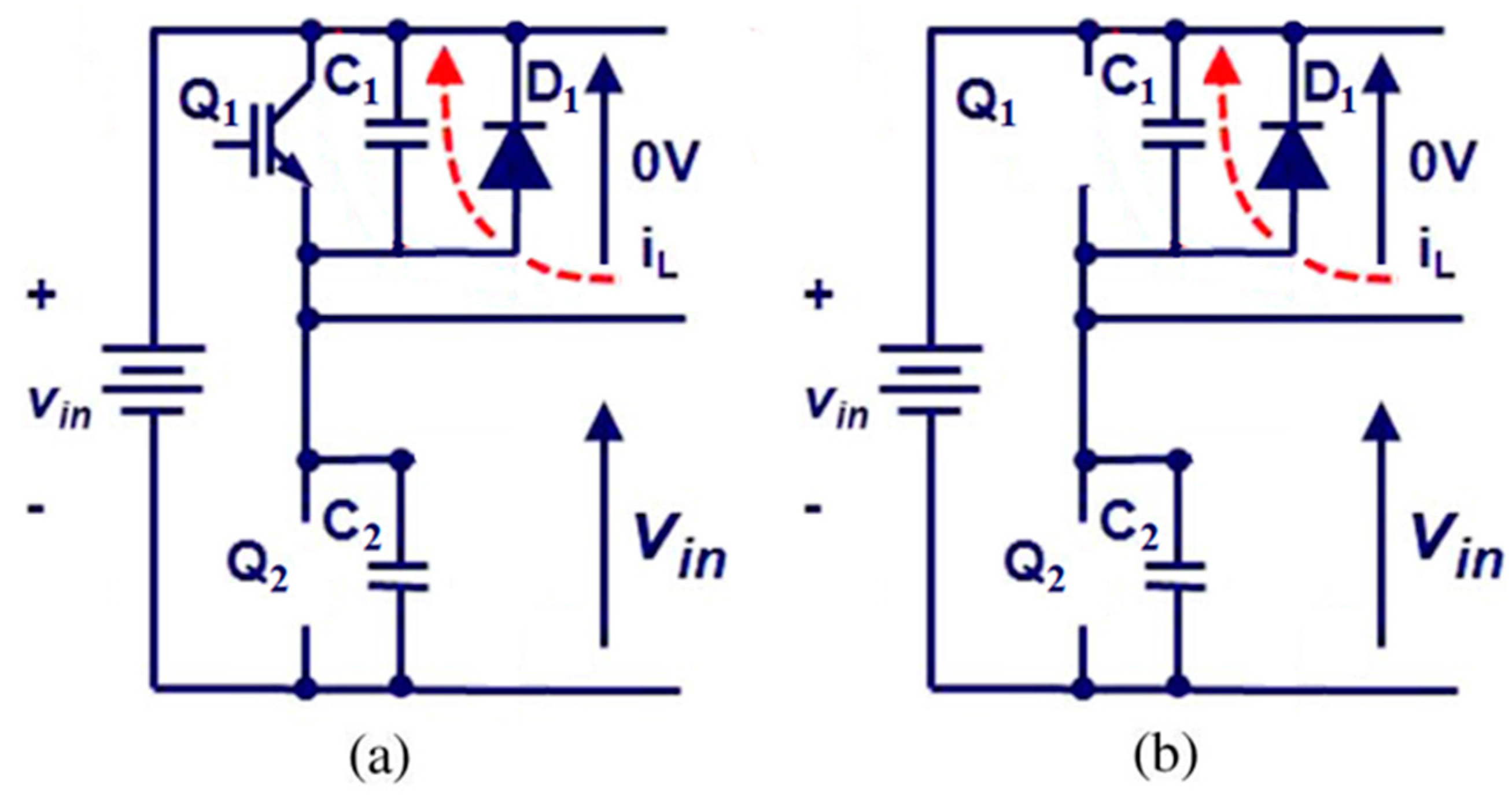
Figure 6.
(a) Initially Q1 is ON and Q2 is OFF. In this case, Q1 is ON but current flows through D1; (b) during switching, Q1 switches OFF before Q2 switches ON. C1 and C2 continue to have 0 V and VIN respectively across their terminals. When Q2 is turned ON, diode D1 will be forced OFF, C1 will be charged up to VIN and C2 will be fully discharged.
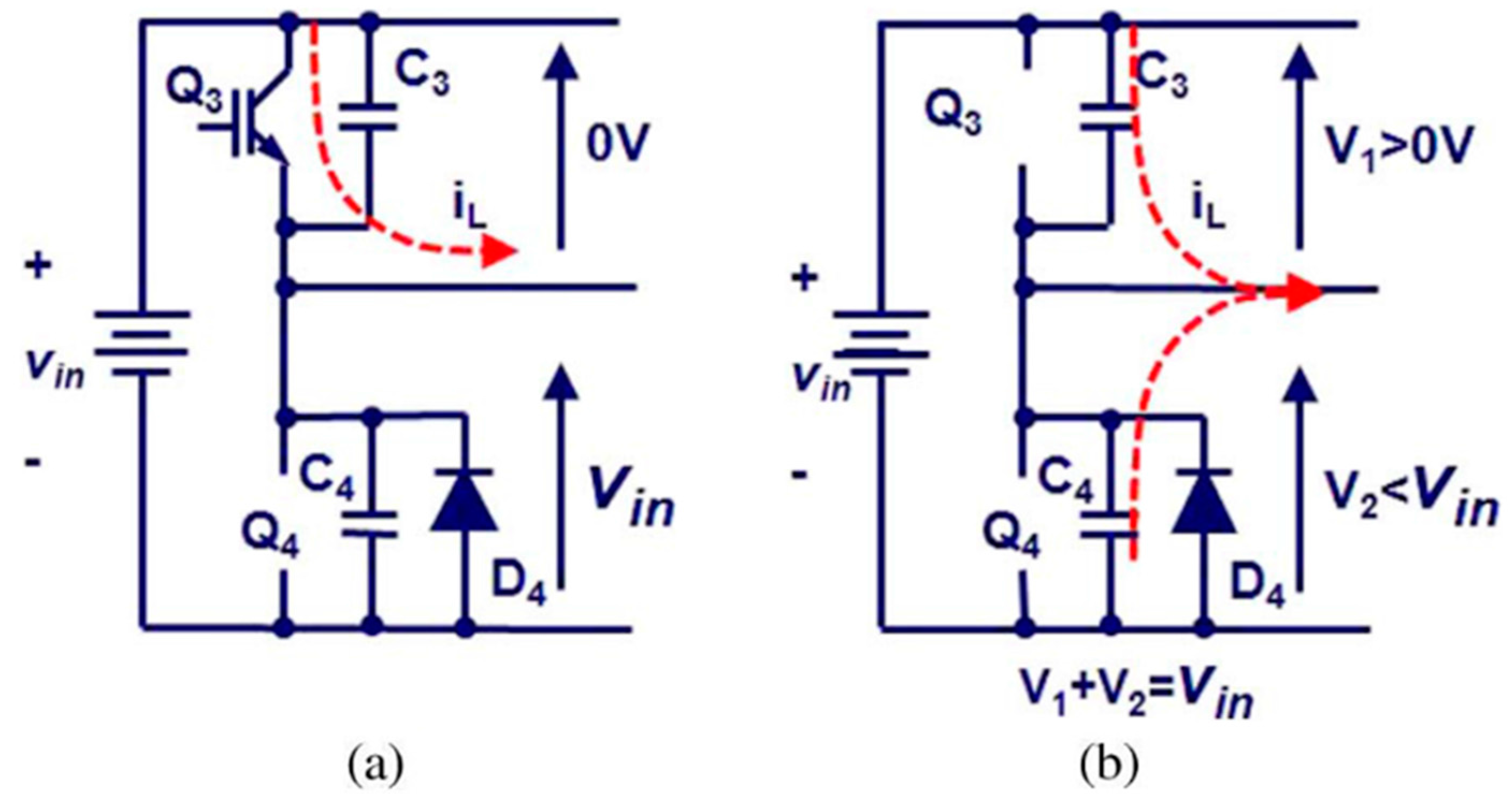
Figure 7.
This figure shows the switching process for leg Q3–Q4. (a) Initially Q3 is ON and Q4 is OFF; In this case (b), Q4 switches ON with zero voltage, because the diode in parallel D4 is conducting. Thus, no turn-on losses are expected in Q4. However, they appear during the OFF transition of Q3.
Figure 8.
(a) Theoretical waveforms of VAB (red) and iPL (blue); (b) Experimental waveforms of VAB (yellow) and iPL (green) scaled to VIN = 80 V, VO = 100 V and PO = 800 W.
Figure 8.
(a) Theoretical waveforms of VAB (red) and iPL (blue); (b) Experimental waveforms of VAB (yellow) and iPL (green) scaled to VIN = 80 V, VO = 100 V and PO = 800 W.
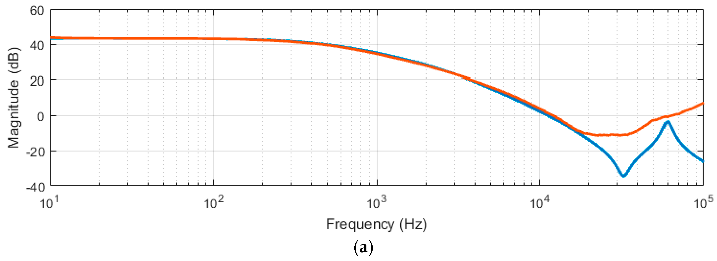
Figure 9.
Experimental (orange) and theoretical (blue) Bode plots for the power source operating on scaled output voltage and power using centered-current control. (a) Magnitude in (dB) and (b) phase in degrees.
Figure 9.
Experimental (orange) and theoretical (blue) Bode plots for the power source operating on scaled output voltage and power using centered-current control. (a) Magnitude in (dB) and (b) phase in degrees.
Figure 10.
Experimental converter used to obtain the Bode diagram and the corresponding waveforms. The transformer has been replaced by discrete LS and CP parts.
Figure 10.
Experimental converter used to obtain the Bode diagram and the corresponding waveforms. The transformer has been replaced by discrete LS and CP parts.
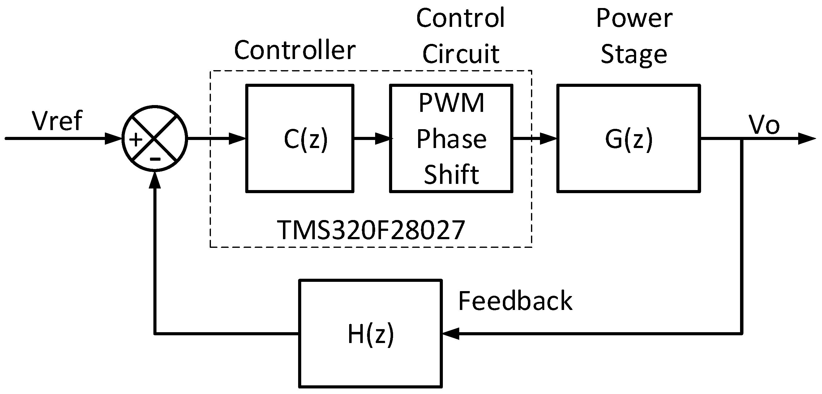
Figure 11.
Digital Feedback system block diagram.
Figure 11.
Digital Feedback system block diagram.
Figure 12.
Experimental waveforms. VAB (yellow), iPL (green), VO (magenta). Bottom: Zoom of the top waveform.
Figure 12.
Experimental waveforms. VAB (yellow), iPL (green), VO (magenta). Bottom: Zoom of the top waveform.
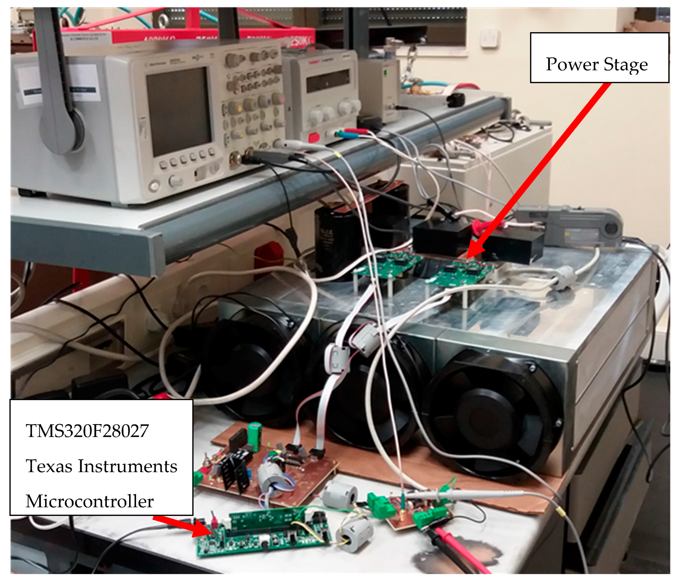
Figure 13.
Converter Test Bench with digital control.
Figure 13.
Converter Test Bench with digital control.
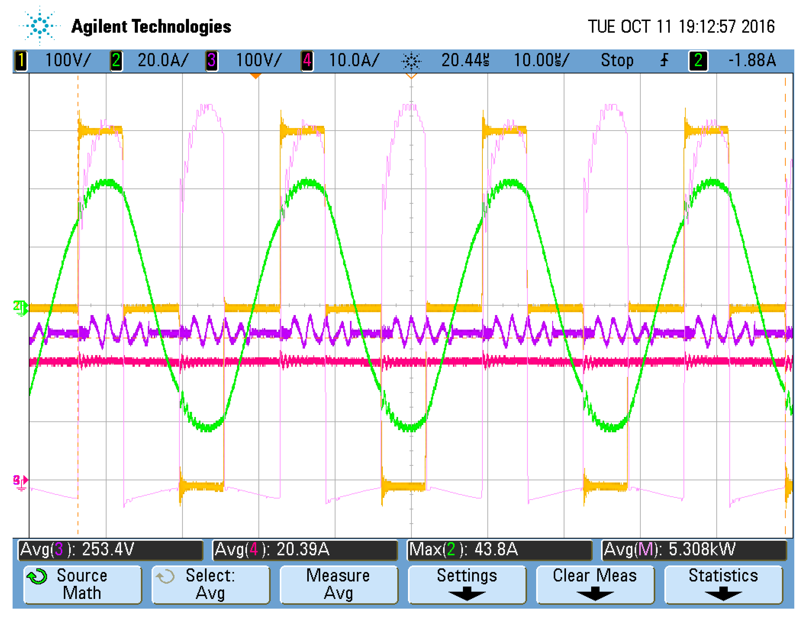
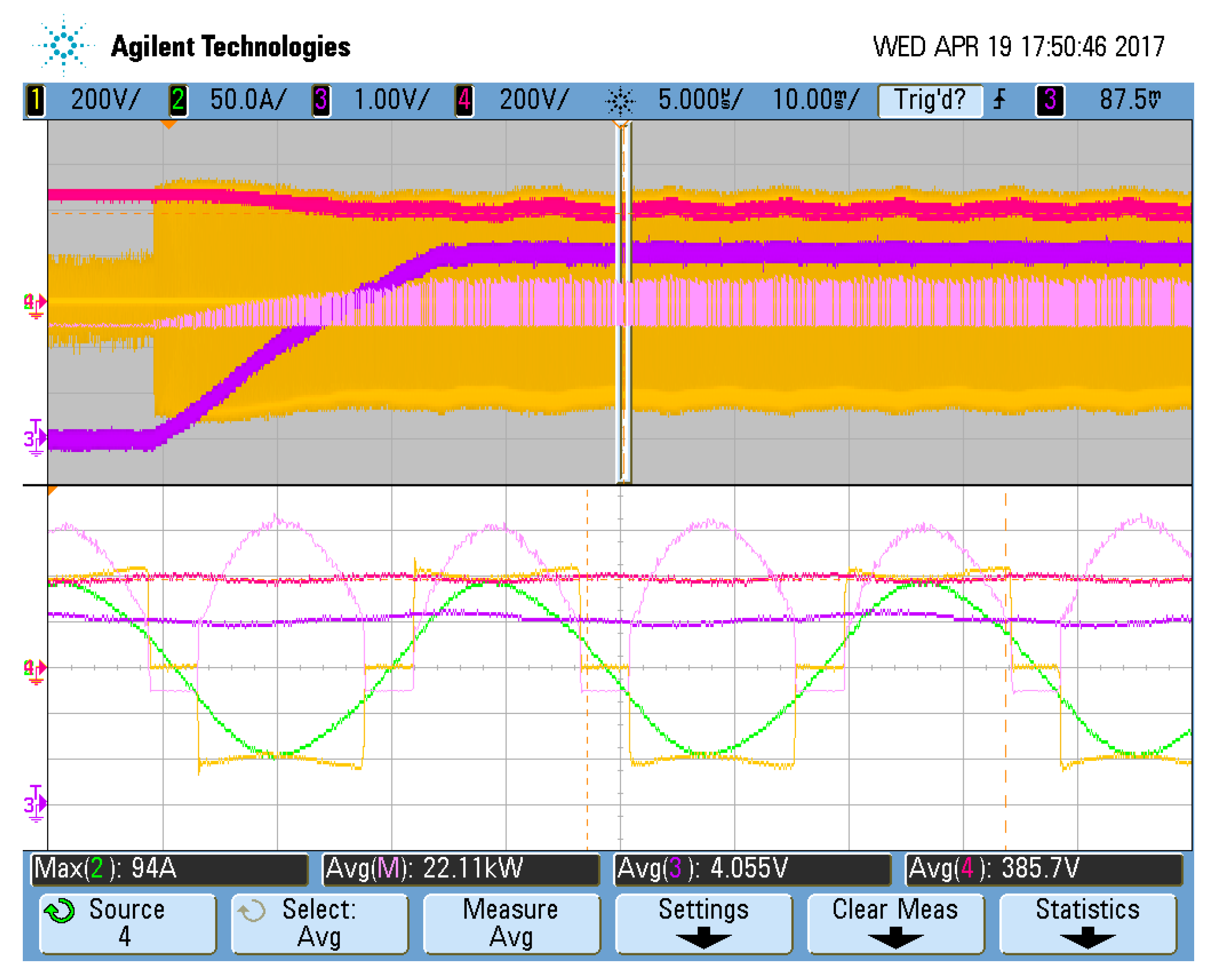
Figure 14.
Experimental waveforms for VAB (yellow) and iPL (green), with Vin = 300 V, VO = 250 V and PO = 5 kW.
Figure 14.
Experimental waveforms for VAB (yellow) and iPL (green), with Vin = 300 V, VO = 250 V and PO = 5 kW.
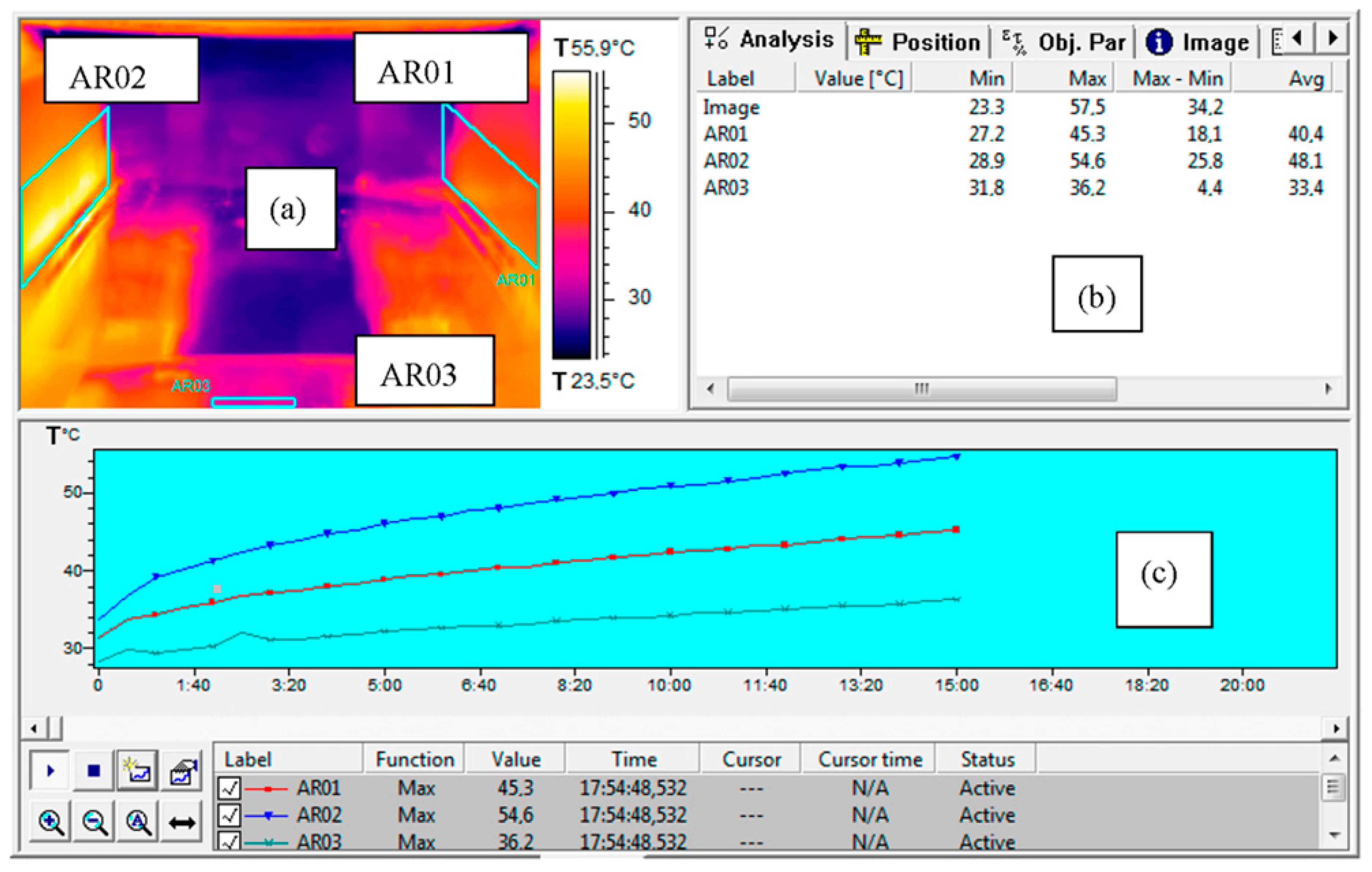
Figure 15.
Temperature Measurement (5 kW) of each leg using IGBTs FF300R12KS4. (a) Infrared image of power stage; (b) Maximum, minimum and difference values measured in each AR0x zone; (c) Temperature evolution in each leg and heatsink; blue: AR02 (Q1–Q2); red: AR01 (Q3–Q4); green: AR03 (heatsink).
Figure 15.
Temperature Measurement (5 kW) of each leg using IGBTs FF300R12KS4. (a) Infrared image of power stage; (b) Maximum, minimum and difference values measured in each AR0x zone; (c) Temperature evolution in each leg and heatsink; blue: AR02 (Q1–Q2); red: AR01 (Q3–Q4); green: AR03 (heatsink).
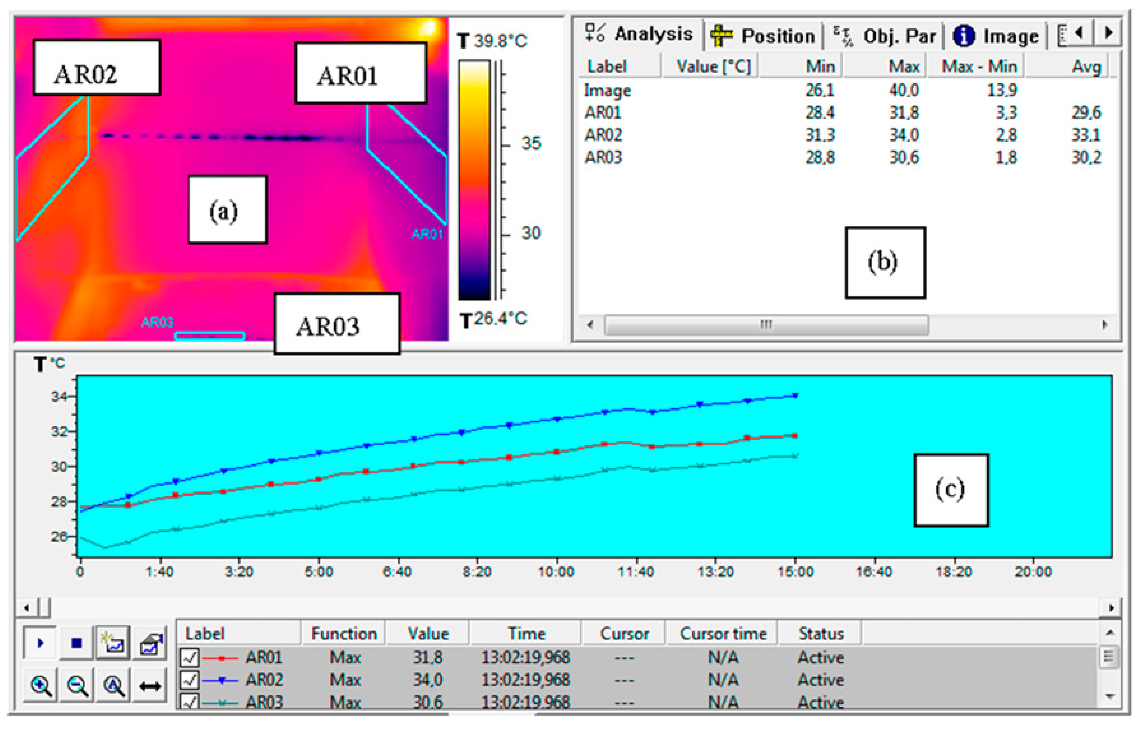
Figure 16.
Temperature Measurement (5 kW) of each leg using MOSFETs CAS300M12BM2. (a) Infrared image of power stage; (b) Maximum, minimum and difference values measured in each AR0x zone; (c) Temperature evolution in each leg and heatsink; blue: AR02 (Q1–Q2); red: AR01 (Q3–Q4); green: AR03 (heatsink).
Figure 17.
Experimental waveforms for VAB (yellow) and iPL (green), with Vin = 400 V, VO = 500 V and PO = 20 kW.
Figure 17.
Experimental waveforms for VAB (yellow) and iPL (green), with Vin = 400 V, VO = 500 V and PO = 20 kW.
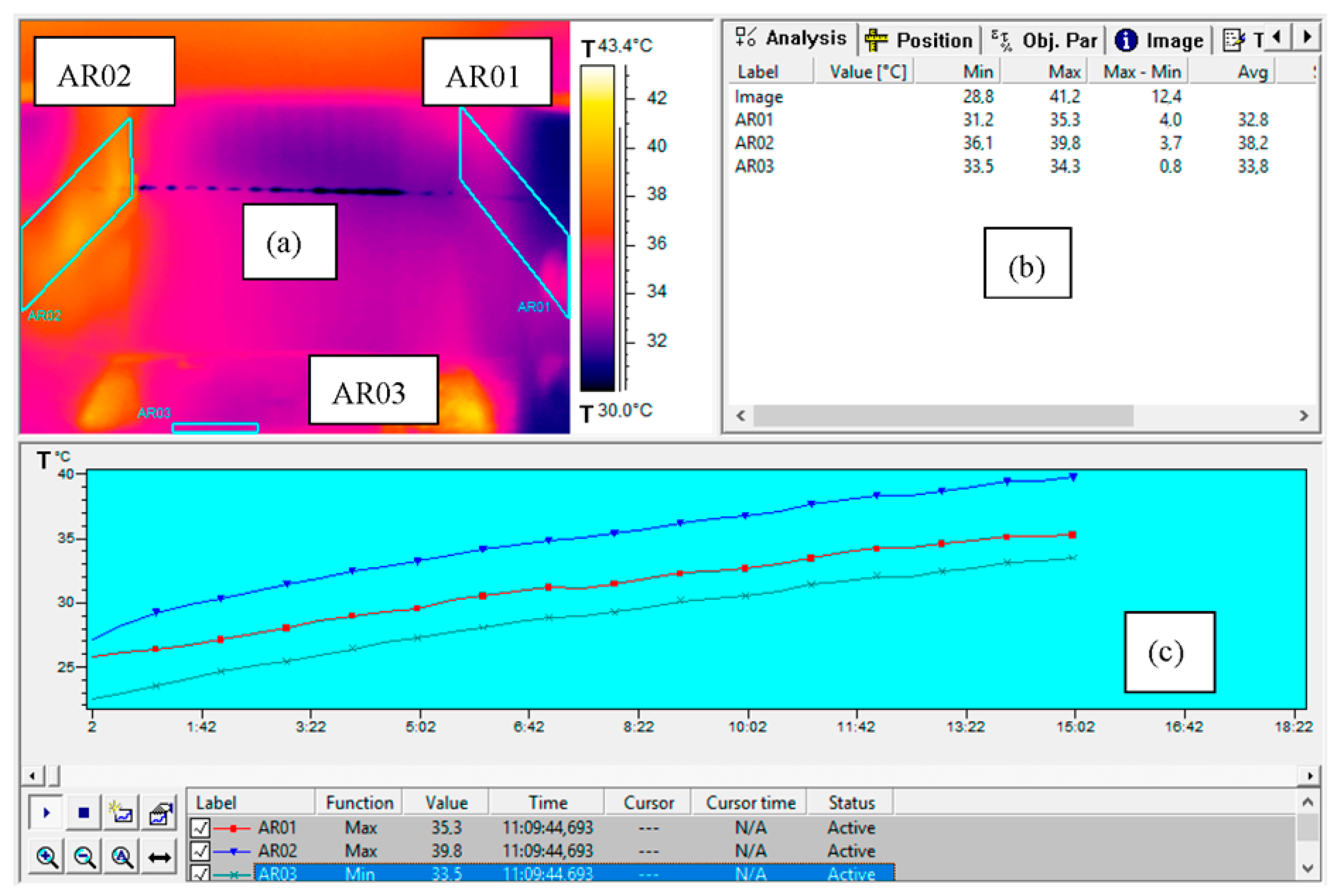
Figure 18.
Temperature Measurement (20 kW) of each leg using MOSFETs CAS300M12BM2. (a) Infrared image of power stage; (b) Maximum, minimum and difference values measured in each AR0x zone; (c) Temperature evolution in each leg and heatsink; blue: AR02 (Q1–Q2); red: AR01 (Q3–Q4); green: AR03 (heatsink).
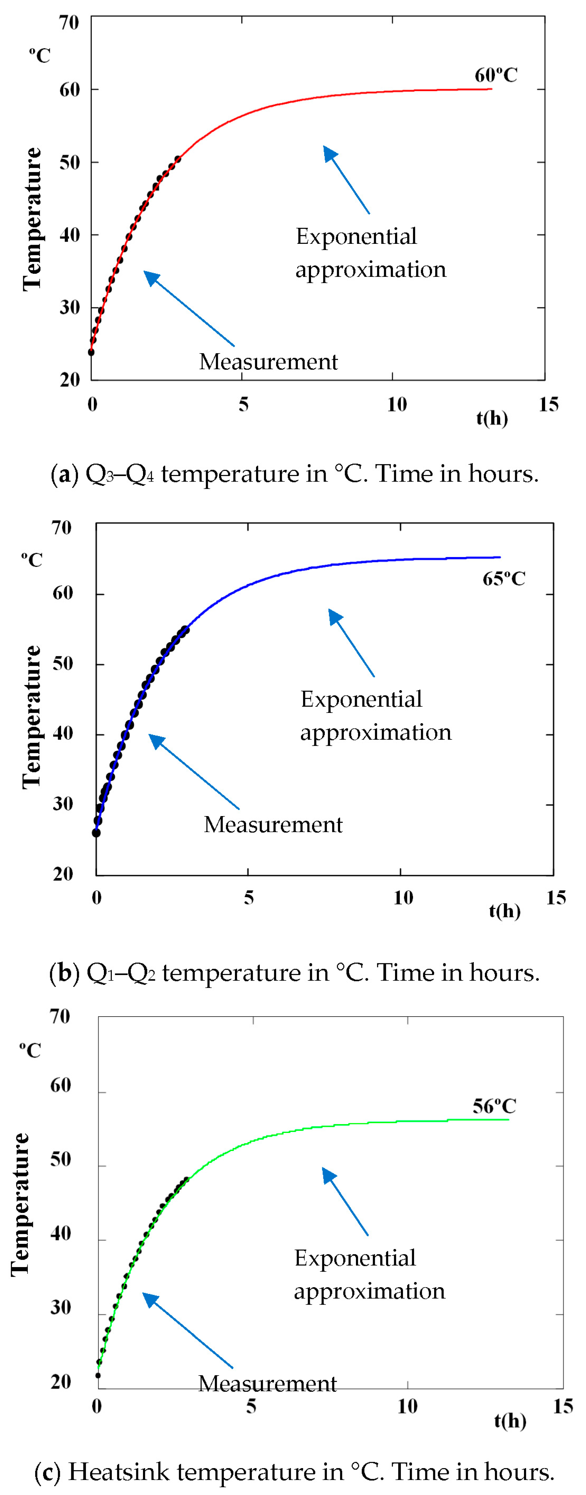
Figure 19.
Measurement of temperature in °C (20 kW) for each leg and for the heatsink using MOSFET CAS300M12BM2 for a time interval of 3 h (dots). Exponential approximations are also included for the temperature (a) in Q3–Q4 (blue), (b) Q1–Q2 (red) and (c) heatsink (green).
Figure 19.
Measurement of temperature in °C (20 kW) for each leg and for the heatsink using MOSFET CAS300M12BM2 for a time interval of 3 h (dots). Exponential approximations are also included for the temperature (a) in Q3–Q4 (blue), (b) Q1–Q2 (red) and (c) heatsink (green).
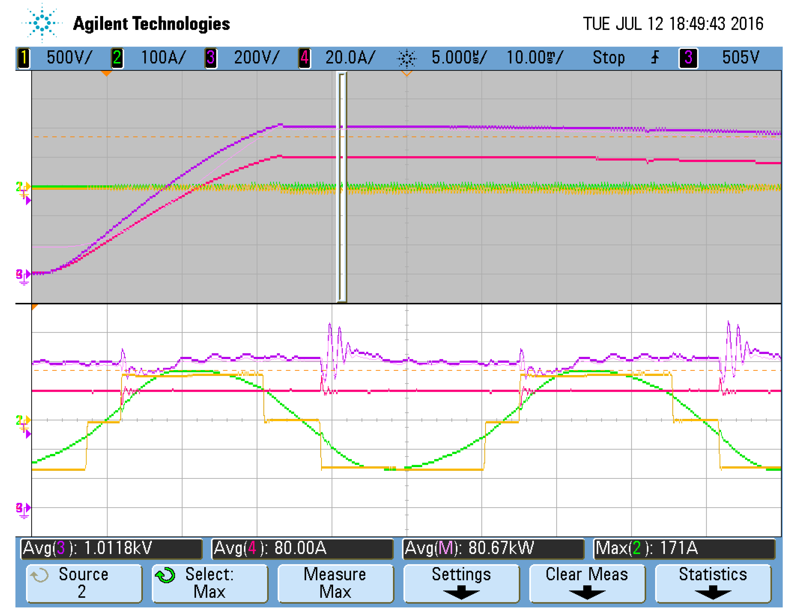
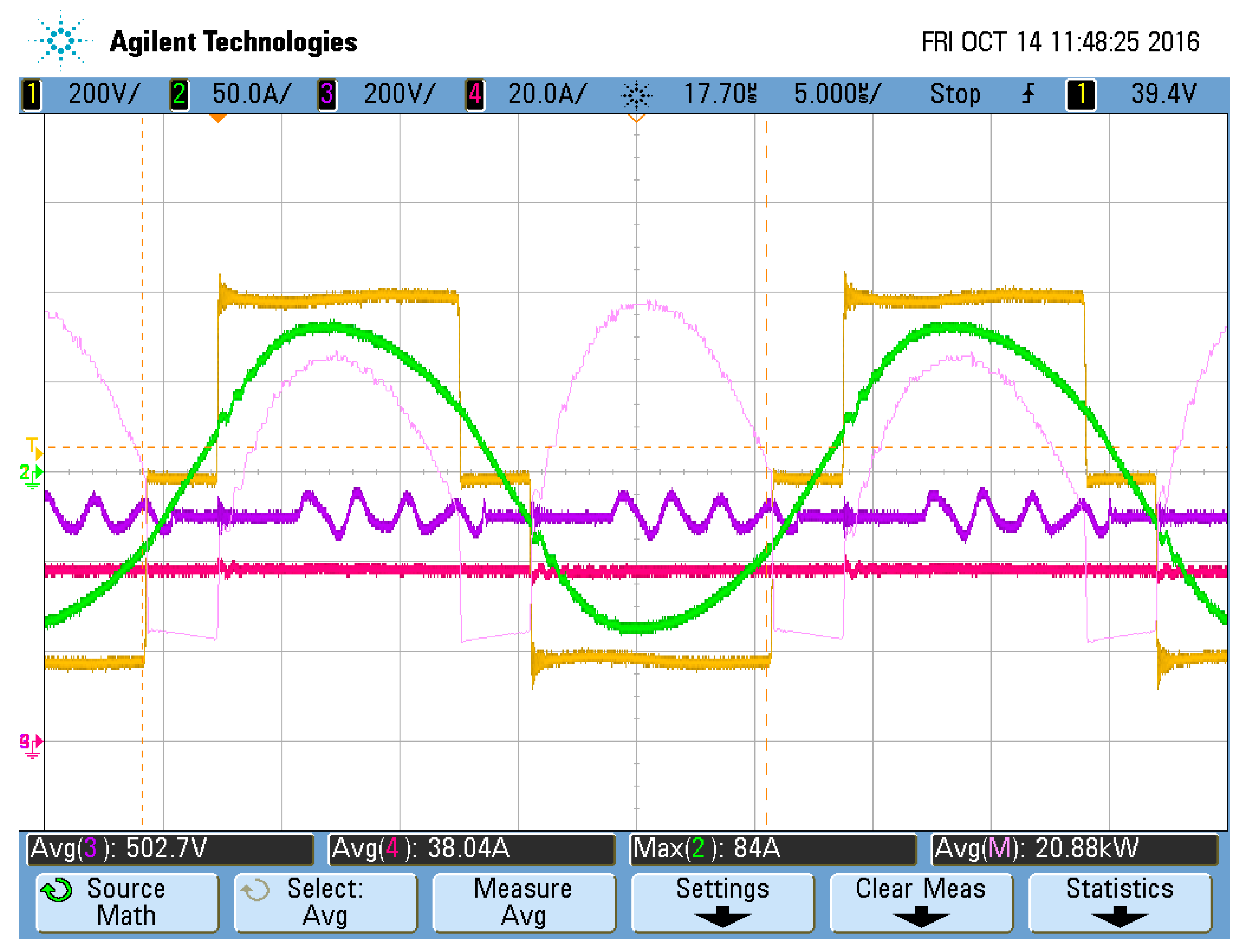
Figure 20.
Experimental waveforms for VAB (yellow) and iPL (green), with VIN = 385 V (red), VO = 40 kV (magenta) and PO = 22 kW.
Figure 20.
Experimental waveforms for VAB (yellow) and iPL (green), with VIN = 385 V (red), VO = 40 kV (magenta) and PO = 22 kW.
Table 1.
Power Dissipation in a Full Bridge at nominal conditions. POUT = 80 kW, VIN = 800 V, VO = 1000 V.
Table 1.
Power Dissipation in a Full Bridge at nominal conditions. POUT = 80 kW, VIN = 800 V, VO = 1000 V.
| POUT = 80 kW VIN = 800 V VO = 1000 V |
|---|
| Power | Q1–Q2 | Q3–Q4 | Total | ηFB |
|---|
| IGBT | 1.71 kW | 836 W | 2.547 kW | 96.9% |
| MOSFET | 503 W | 237 W | 740 W | 99% |
Table 2.
Temperature Measurements for PO = 5 kW in SiC MOSFET and Si IGBT after 15 min.
Table 2.
Temperature Measurements for PO = 5 kW in SiC MOSFET and Si IGBT after 15 min.
| PO = 5 kW VIN = 300 V VO = 250 V |
|---|
| Temperature | TQ1–Q2 | TQ3–Q4 | THeatsink |
|---|
| IGBT | 54.6 °C | 45.3 °C | 36.2 °C |
| MOSFET | 34 °C | 31.8 °C | 30.6 °C |
Table 3.
Temperature Measurements for PO = 20 kW in SiC MOSFET after 15 min.
Table 3.
Temperature Measurements for PO = 20 kW in SiC MOSFET after 15 min.
| PO = 20 kW VIN = 400 V VO = 500 V |
|---|
| Temperature | TQ1–Q2 | TQ3–Q4 | THeatsink |
|---|
| MOSFET | 39.9 °C | 35.3 °C | 34.3 °C |
Table 4.
Temperature Measurements for SiC MOSFET and Si IGBT after 15 min for 5 kW and 20 kW.
Table 4.
Temperature Measurements for SiC MOSFET and Si IGBT after 15 min for 5 kW and 20 kW.
| POUT = 20 kW VIN = 400 V VO = 500 V |
| Temperature | TQ1–Q2 | TQ3–Q4 | THeatsink |
| MOSFET | 39.9 °C | 35.3 °C | 34.3 °C |
| POUT = 5 kW VIN = 300 V VO = 250 V |
| IGBT | 54.6 °C | 45.3 °C | 36.2 °C |
| MOSFET | 34 °C | 31.8 °C | 30.6 °C |
Table 5.
Theoretical Power Dissipation in Full Bridge topology.
Table 5.
Theoretical Power Dissipation in Full Bridge topology.
| POUT = 80 kW VIN = 800 V VO = 1000 V |
| Power | Q1–Q2 | Q3–Q4 | Total | ηFB |
| IGBT | 1.71 kW | 836 W | 2.547 kW | 96.9% |
| MOSFET | 503 W | 237 W | 740 W | 99% |
| POUT = 20 kW VIN = 400 V VO = 500 V |
| IGBT | 515 W | 239 W | 755 W | 96.3% |
| MOSFET | 107 W | 47 W | 154 W | 99.2% |
| POUT = 5 kW VIN = 300 V VO = 250 V |
| IGBT | 407 W | 166 W | 573 W | 89.7% |
| MOSFET | 70 W | 28 W | 98 W | 98% |

 ,
, 


