
Crosstalk Study of Simultaneous Wireless Power/Information Transmission Based on an LCC Compensation Network

Abstract
:1. Introduction
2. Overviews of SWTPI and the LCC Compensation Network
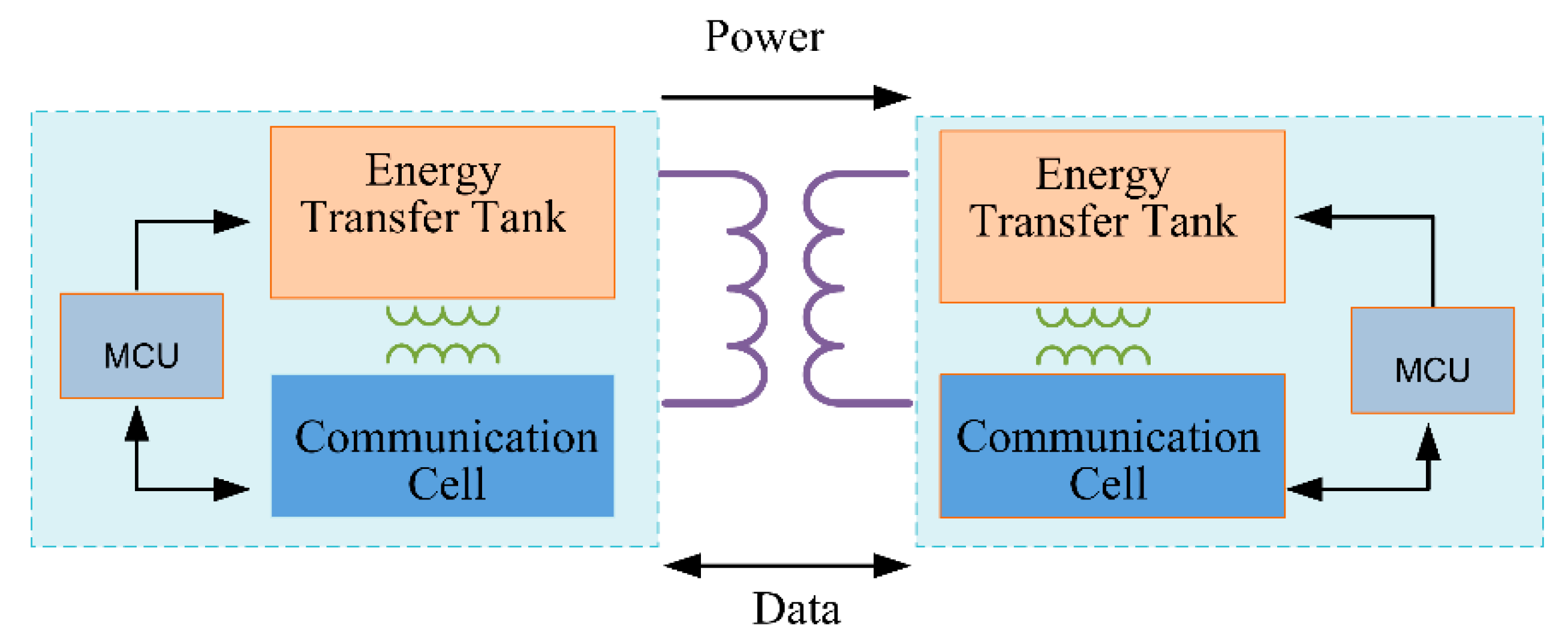
2.1. Overview of SWTPI
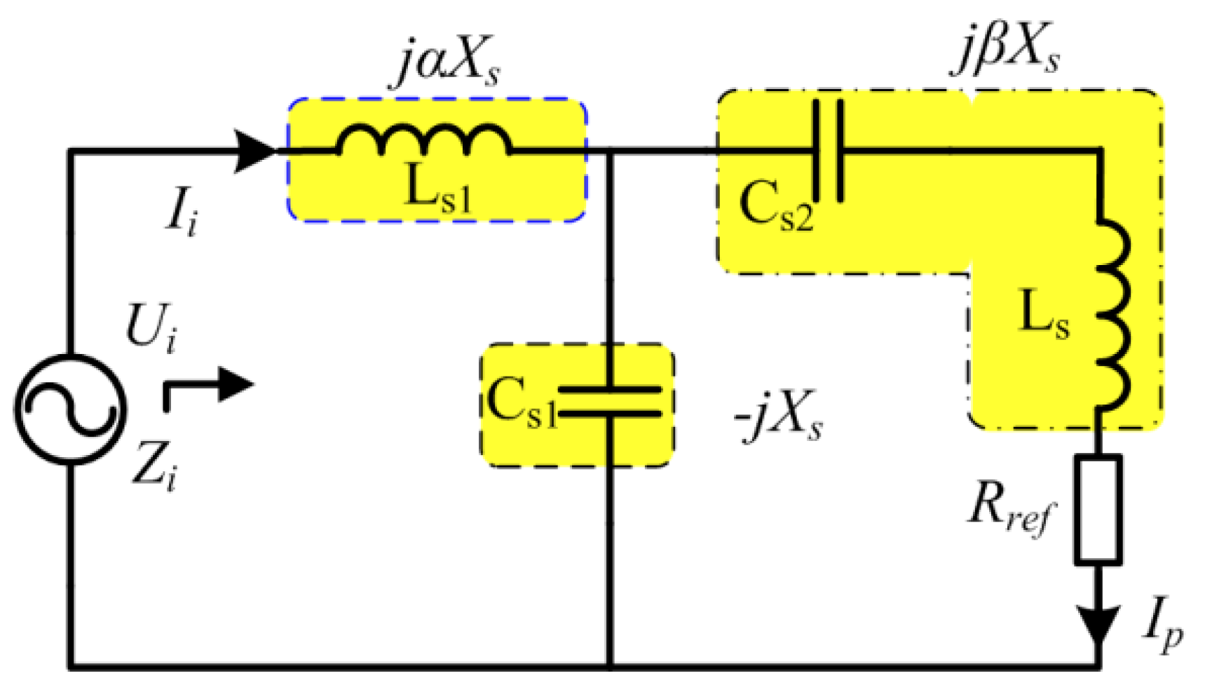
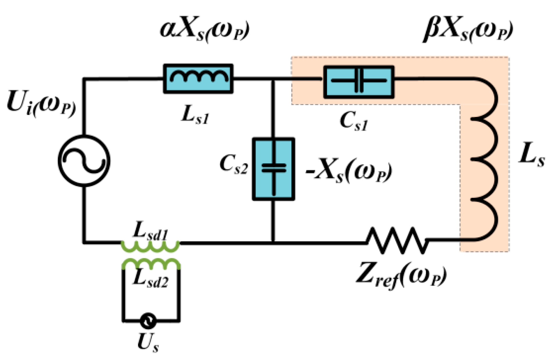
2.2. Overview of the LCC Compensation Network
- (1)
- The overall impedance from the input side becomes
- (2)
- Using Equation (1), the output current flowing through Rref can be derived as
3. Crosstalk Study of SWTPI Based on the LCC Compensation Network
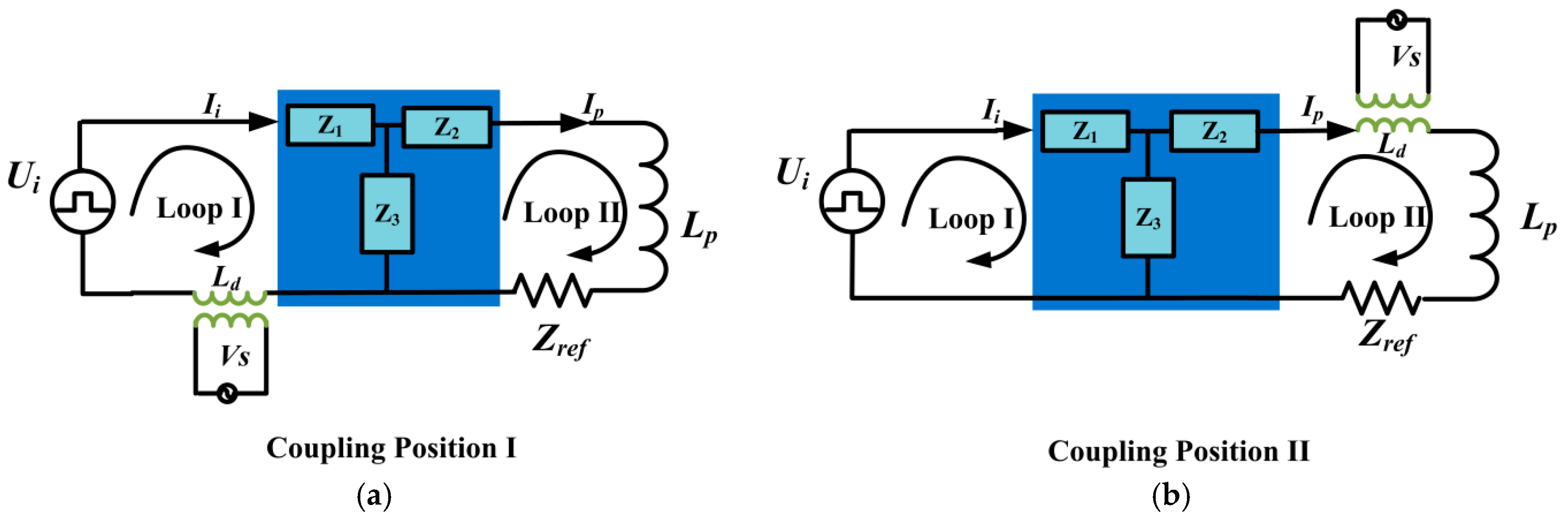
3.1. Selection of Compensation Network and Coupling Position
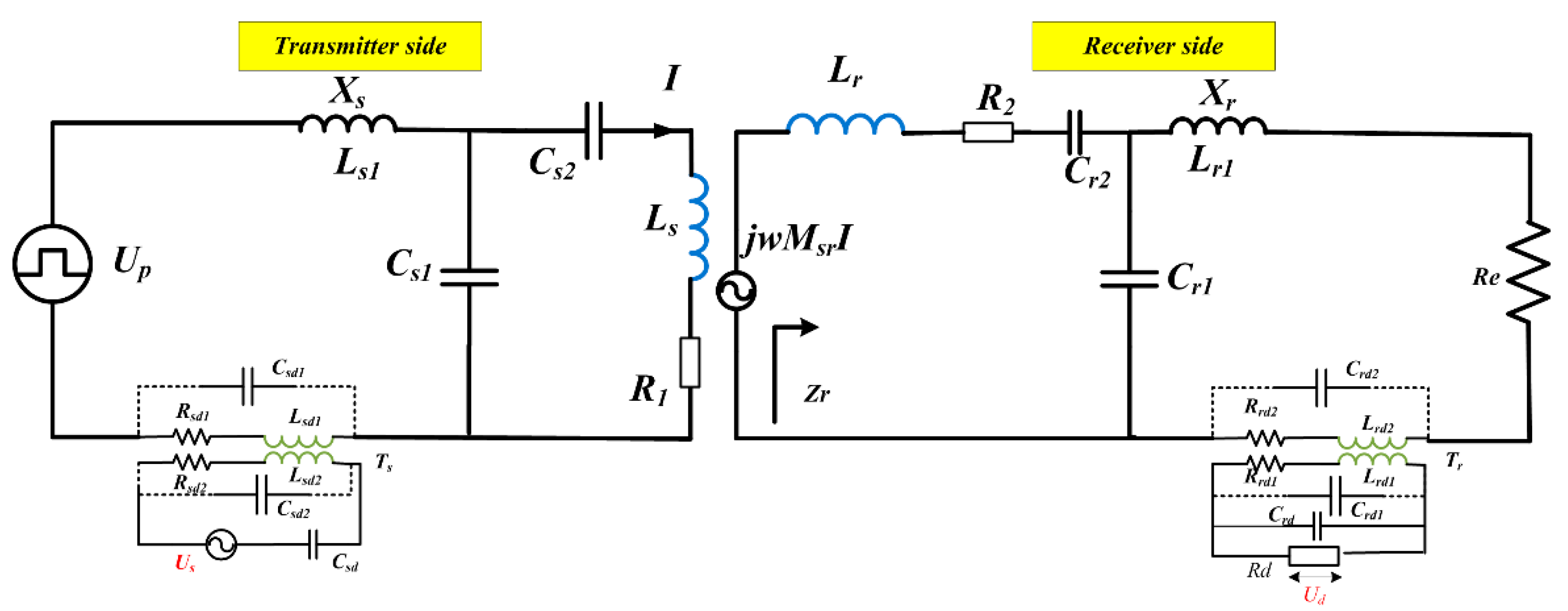
3.2. Proposed Structure
3.3. Data Transmission Analysis
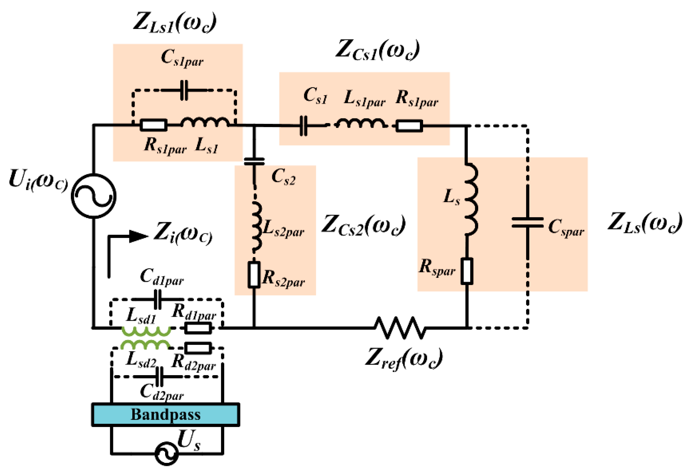
3.4. Crosstalk at the Power Frequency Based on the LCC Compensation Network
3.5. Crosstalk at the Communication Frequency Based on the LCC Compensation Network
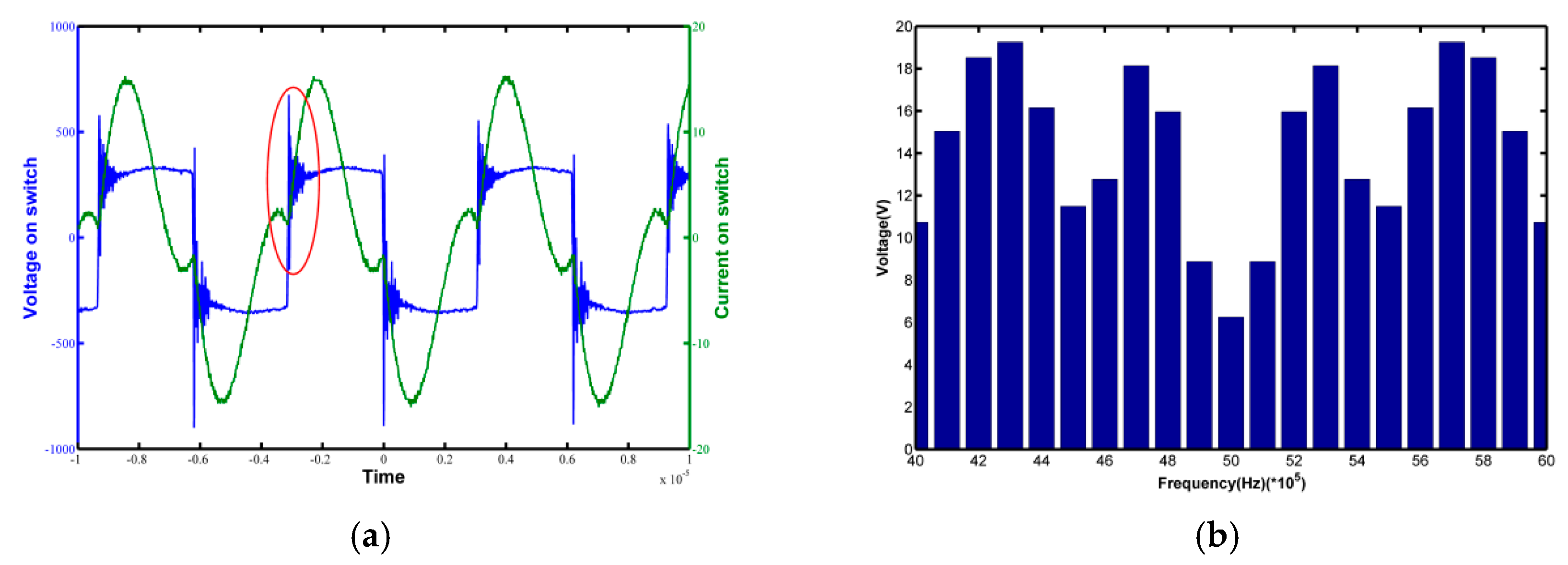
3.6. Crosstalk from the Switch Process of the Inverter
3.7. Influence of Misalignment on Crosstalk
4. Crosstalk Minimization via Parameter Design for the LCC Compensation Network
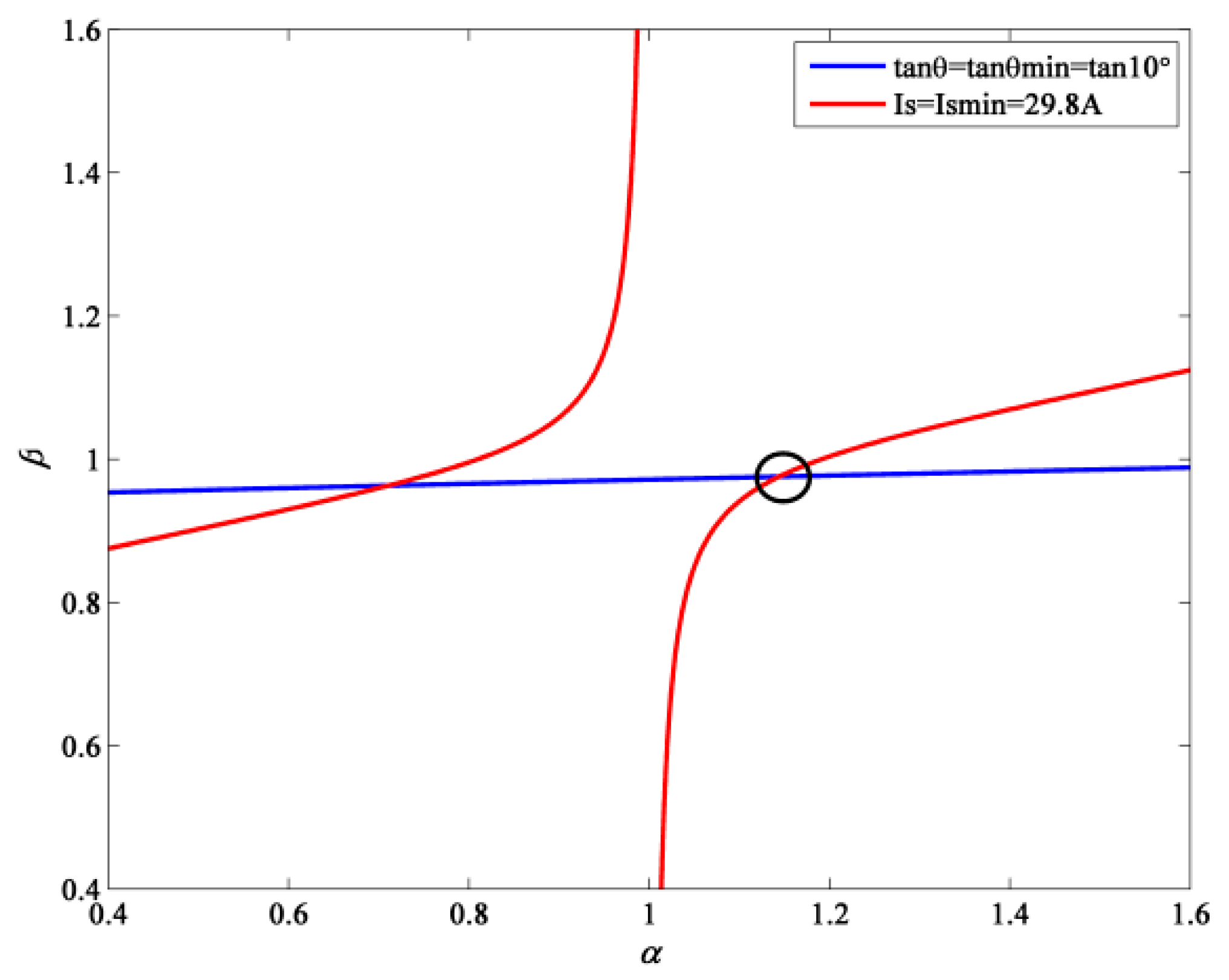
4.1. Minimizing the Crosstalk at the Power Frequency and Communication Frequency
4.2. Ensuring the ZVS Status of the Inverter
4.3. Parameter Design Method for the LCC Compensation Network to Minimize the Crosstalk
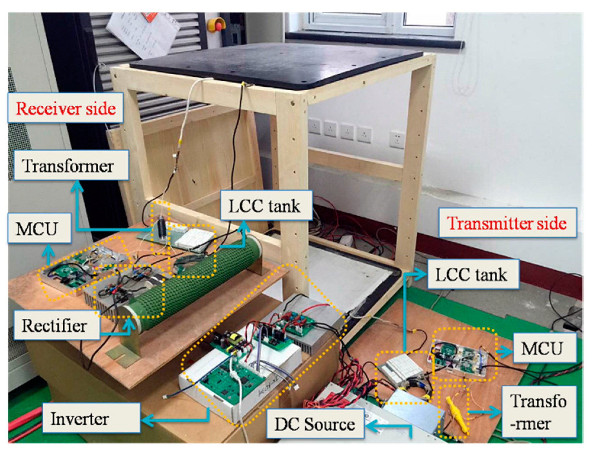
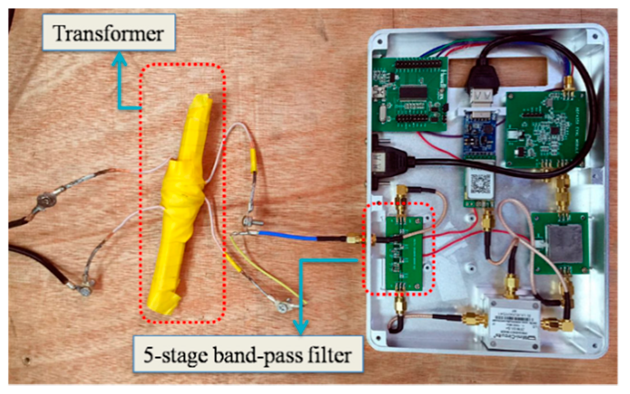
5. Prototype Design and Experimental Validation
5.1. Experimental Set
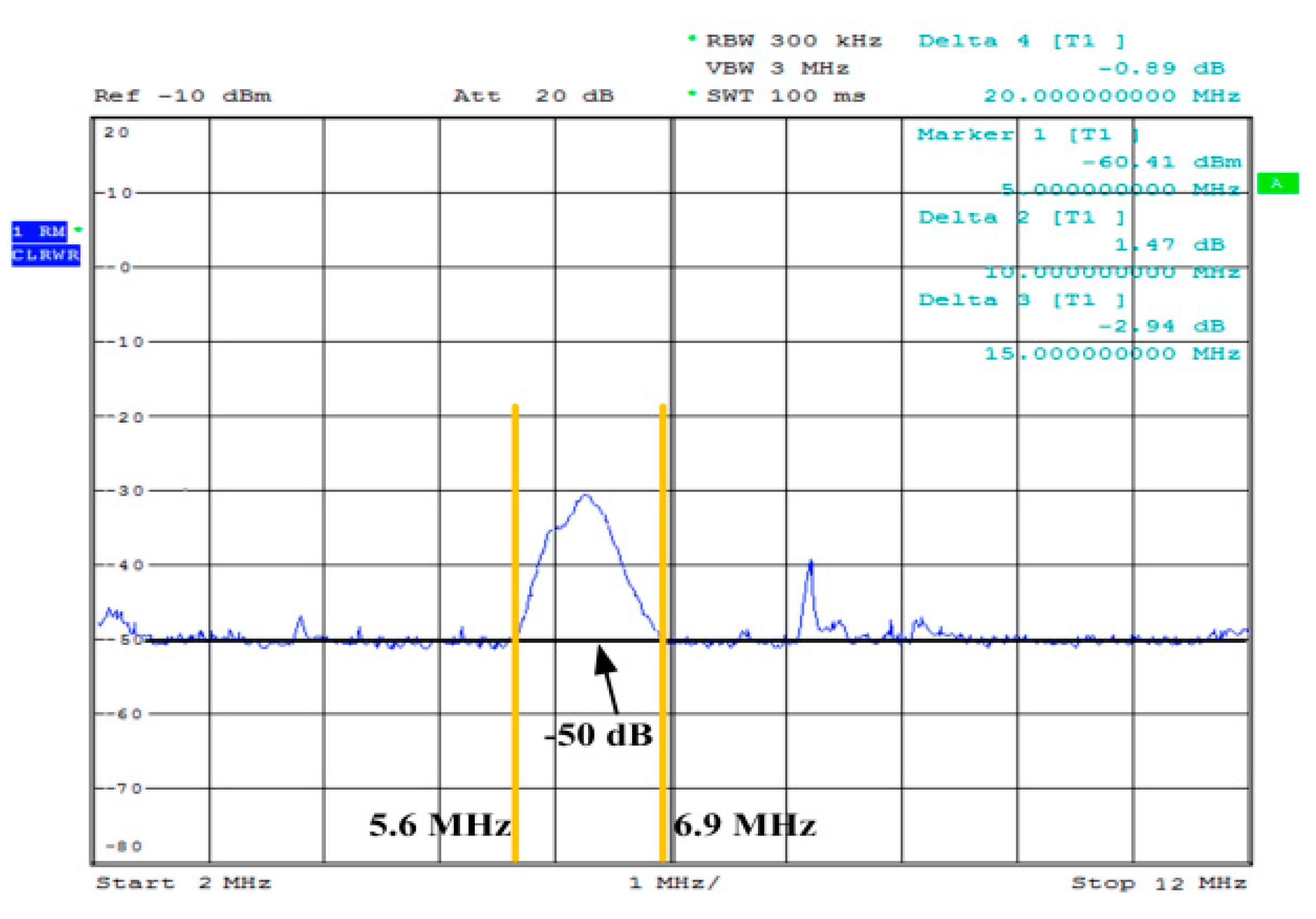
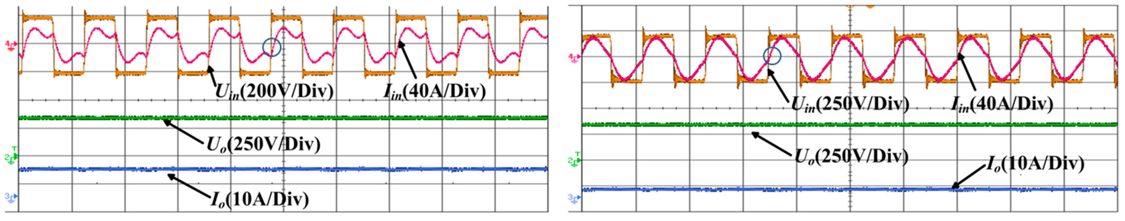
5.2. Experimental Results
6. Conclusions
Acknowledgments
Author Contributions
Conflicts of Interest
References
- Li, S.Q.; Mi, C.C. Wireless Power Transfer for Electric Vehicle Applications. IEEE J. Emerg. Sel. Top. Power Electron. 2015, 3, 4–17. [Google Scholar]
- Choi, S.Y.; Gu, B.W.; Jeong, S.Y.; Rim, C.T. Advances in Wireless Power Transfer Systems for Roadway-Powered Electric Vehicles. IEEE J. Emerg. Sel. Top. Power Electron. 2015, 3, 18–36. [Google Scholar] [CrossRef]
- Chopra, S.; Bauer, P. Driving Range Extension of EV with On-Road Contactless Power Transfer-A Case Study. IEEE Trans. Ind. Electron. 2013, 60, 329–338. [Google Scholar] [CrossRef]
- Zhu, Q.; Guo, Y.; Wang, L.; Liao, C.; Li, F. Improving the Misalignment Tolerance of Wireless Charging System by Optimizing the Compensate Capacitor. IEEE Trans. Ind. Electron. 2015, 62, 4832–4836. [Google Scholar] [CrossRef]
- Baker, T.; NgokoM, Y.; Calasan, R.T. Energy Efficient Cloud Computing Environment via Autonomic Meta-director Framework. In Proceedings of the 2013 Sixth International Conference on Developments in eSystems Engineering (DeSE), Abu Dhabi, UAE, 16–18 December 2013. [Google Scholar]
- Baker, T.; Al-Dawsari, B.; Tawfik, H.; Reid, D.; Ngoko, Y. GreeDi: An energy efficient routing algorithm for big data on cloud. Ad Hoc Netw. 2015, 35, 83–96. [Google Scholar] [CrossRef]
- Aldawsari, B.; Baker, T.; England, D. Trusted Energy-Efficient Cloud-Based Services Brokerage Platform. Int. J. Intell. Comput. Res. 2015, 6, 630–639. [Google Scholar] [CrossRef]
- Esteban, B.; Sid-Ahmed, M.; Kar, N.C. A Comparative Study of Power Supply Architectures in Wireless EV Charging Systems. IEEE Trans. Power Electron. 2015, 30, 6408–6422. [Google Scholar] [CrossRef]
- Rush, A.D.; Troyk, P.R. A Power and Data Link for a Wireless-Implanted Neural Recording System. IEEE Trans. Biomed. Eng. 2012, 59, 3255–3262. [Google Scholar] [CrossRef] [PubMed]
- Wang, Z.; Li, Y.; Sun, Y.; Tang, C.; Lv, X. Load Detection Model of Voltage-Fed Inductive Power Transfer System. IEEE Trans. Power Electron. 2013, 28, 5233–5243. [Google Scholar] [CrossRef]
- Ju, X.; Dong, L.; Huang, X.; Liao, X. Switching Technique for Inductive Power Transfer at High-Q Regimes. IEEE Trans. Ind. Electron. 2015, 62, 2164–2173. [Google Scholar] [CrossRef]
- Li, W.; Yuan, H.; Xu, W.; Geng, K.; Wang, G. An Optimization Procedure for Coil Design in a Dual Band Wireless Power and Data Transmission System. ECS Trans. 2013, 52, 1091–1097. [Google Scholar] [CrossRef]
- Wang, G.; Liu, W.L.W.; Sivaprakasam, M.; Zhou, M.; Weiland, J.D.; Humayun, M.S. A Dual Band Wireless Power and Data Telemetry for Retinal Prosthesis. In Proceedings of the International Conference 2006 of the IEEE Engineering in Medicine and Biology Society, New York, NY, USA, 30 August–3 September 2006. [Google Scholar]
- Xu, Q.; Hu, D.; Duan, B.; He, J. A Fully Implantable Stimulator with Wireless Power and Data Transmission for Experimental Use in Epidural Spinal Cord Stimulation. IEEE Trans. Neural Syst. Rehabil. 2015, 23, 683–692. [Google Scholar] [CrossRef] [PubMed]
- Kilinc, E.G.; Baj-Rossi, C.; Ghoreishizadeh, S.; Riario, S.; Stradolini, F.; Boero, C.; De Micheli, G.; Maloberti, F.; Carrara, S. A System for Wireless Power Transfer and Data Communication of Long-Term Bio-Monitoring. IEEE Sens. J. 2015, 15, 6559–6569. [Google Scholar] [CrossRef]
- Wang, G.X.; Wang, P.J.; Tang, Y.N.; Liu, W.T. Analysis of Dual Band Power and Data Telemetry for Biomedical Implants. IEEE Trans. Biomed. Circuits Syst. 2012, 6, 208–215. [Google Scholar] [CrossRef] [PubMed]
- Hirai, J.; Kim, T.W.; Kawamura, A. Study on crosstalk in inductive transmission of power and information. IEEE Trans. Ind. Electron. 1999, 46, 1174–1182. [Google Scholar] [CrossRef]
- Wu, J.; Zhao, C.; Lin, Z.; Du, J.; Hu, Y.; He, X. Wireless Power and Data Transfer via a Common Inductive Link Using Frequency Division Multiplexing. IEEE Trans. Ind. Electron. 2015, 62, 7810–7820. [Google Scholar] [CrossRef]
- Yilmaz, G.; Dehollain, C. Single frequency wireless power transfer and full-duplex communication system for intracranial epilepsy monitoring. Microelectron. J. 2014, 45, 1595–1602. [Google Scholar] [CrossRef]
- Yilmaz, G.; Atasoy, O.; Dehollain, C. Wireless Energy and Data Transfer for In-Vivo Epileptic Focus Localization. IEEE Sens. J. 2013, 13, 4172–4179. [Google Scholar] [CrossRef]
- Hirai, J.; Kim, T.W.; Kawamura, A. Integral motor with driver and wireless transmission of power and information for autonomous subspindle drive. IEEE Trans. Power Electron. 2000, 15, 13–20. [Google Scholar] [CrossRef]
- Hirai, J.; Kim, T.-W.; Kawamura, A. Study on intelligent battery charging using inductive transmission of power and information. IEEE Trans. Power Electron. 2000, 15, 335–345. [Google Scholar] [CrossRef]
- Hirai, J.; Tae-Woong, K.; Kawamura, A. Wireless transmission of power and information and information for cableless linear motor drive. IEEE Trans. Power Electron. 2000, 15, 21–27. [Google Scholar] [CrossRef]
- Van Boheemen, E.L.; Boys, J.T.; Covic, G.A. Dual-tuning IPT systems for low bandwidth communications. In Proceedings of the 2007 2nd IEEE Conference on Industrial Electronics and Applications, Harbin, China, 23–25 May 2007. [Google Scholar]
- Zhu, Q.; Wang, L.; Guo, Y.; Liao, C.; Li, F. Applying LCC Compensation Network to Dynamic Wireless EV Charging System. IEEE Trans. Ind. Electron. 2016, 63, 6557–6567. [Google Scholar] [CrossRef]
- Li, W.; Zhao, H.; Deng, J.; Li, S.; Mi, C.C. Comparison Study on SS and double-sided LCC compensation topologies for EV/PHEV Wireless Chargers. IEEE Trans. Veh. Technol. 2016, 65, 4429–4439. [Google Scholar] [CrossRef]
- Li, S.; Li, W.; Deng, J.; Nguyen, T.D.; Mi, C.C. A Double-Sided LCC Compensation Network and Its Tuning Method for Wireless Power Transfer. IEEE Trans. Veh. Technol. 2015, 64, 2261–2273. [Google Scholar] [CrossRef]
- Li, W.; Zhao, H.; Li, S.; Deng, J.; Kan, T.; Mi, C.C. Integrated LCC Compensation Topology for Wireless Charger in Electric and Plug-in Electric Vehicles. IEEE Trans. Ind. Electron. 2015, 62, 4215–4225. [Google Scholar] [CrossRef]
- Feng, H.; Cai, T.; Duan, S.; Zhao, J.; Zhang, X.; Chen, C. An LCC-Compensated Resonant Converter Optimized for Robust Reaction to Large Coupling Variation in Dynamic Wireless Power Transfer. IEEE Trans. Ind. Electron. 2016, 63, 6591–6601. [Google Scholar] [CrossRef]
- Zhou, S.; Mi, C.C. Multi-Paralleled LCC Reactive Power Compensation Networks and Their Tuning Method for Electric Vehicle Dynamic Wireless Charging. IEEE Trans. Ind. Electron. 2016, 63, 6546–6556. [Google Scholar] [CrossRef]
- Pantic, Z.; Bai, S.; Lukic, S.M. ZCS LCC-Compensated Resonant Inverter for Inductive-Power-Transfer Application. IEEE Trans. Ind. Electron. 2011, 58, 3500–3510. [Google Scholar] [CrossRef]
- Geng, Y.; Li, B.; Yang, Z.; Lin, F.; Sun, H. A High Efficiency Charging Strategy for a Supercapacitor Using a Wireless Power Transfer System Based on Inductor/Capacitor/Capacitor (LCC) Compensation. Energies 2017, 10, 10135. [Google Scholar] [CrossRef]
- Mai, R.; Chen, Y.; Liu, Y. Compensation Capacitor Alteration Based IPT Battery Charging Application With Constant Current and Constant Voltage Control. In Proceedings of the Chinese Society of Electrical Engineering, Beijing, China, 10–13 August 2016. [Google Scholar]


| Parameter | Value |
|---|---|
| Air gap | 100 cm |
| Udc | 210 V |
| fp | 160 kHz |
| fd | 6 MHz |
| Ls, Lr | 119 μH, 120 μH |
| rLs, rlr2 | 208 mΩ, 263 mΩ |
| Ls1, Lr1 | 8.36 μH, 7.1 μH |
| Cs1, Cs2, Cr1, Cr2 | 120 nF, 8.9 nF, 139 nF, 9 nF |
| Lsd1, Lsd2, Ld1, Lrd1 | 2 μH |
| rsd1, rsd2, rrd1, rrd2 | 10 Ω |
| Csd, Crd | 50 pF |
| Msr | 1.98 μH |
| Mts, Mtr | ≈2 μH |
| Xs, Xr | 6.97 Ω, 7.14 Ω |
| Rl | 22.4 Ω–30.4 Ω |
| Misalignment | 30 cm |
| α, β | 1.085, 0.932 |
| Parameter | Value (Avg) |
|---|---|
| Vs | 3150 V |
| Vsd1(Proposed) | 14.5 V |
| Vsd1(Previous) | 52.5 V |
| Vr | 3048 V |
| Vrd1(Proposed) | 1.83 V |
| Vrd1(Previous) | 50.8 V |
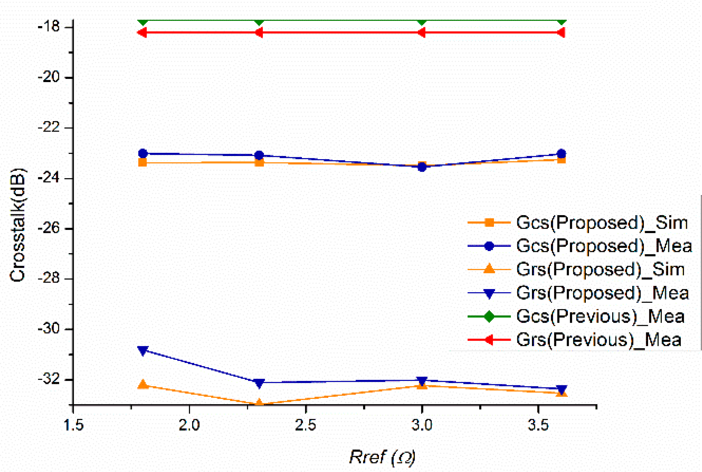
| Reflected Load | Power In | Power Received | SNR |
|---|---|---|---|
| 1.8 Ω | −20 dBmW | −35 dBmW | 9 dB |
| 2.3 Ω | −22 dBmW | −32 dBmW | 10 dB |
| 3 Ω | −19 dBmW | −30 dBmW | 10 dB |
| 3.6 Ω | −21 dBmW | −33 dBmW | 11 dB |
© 2017 by the authors. Licensee MDPI, Basel, Switzerland. This article is an open access article distributed under the terms and conditions of the Creative Commons Attribution (CC BY) license (http://creativecommons.org/licenses/by/4.0/).
Share and Cite
Ji, L.; Wang, L.; Liao, C.; Li, S. Crosstalk Study of Simultaneous Wireless Power/Information Transmission Based on an LCC Compensation Network. Energies 2017, 10, 1606. https://doi.org/10.3390/en10101606
Ji L, Wang L, Liao C, Li S. Crosstalk Study of Simultaneous Wireless Power/Information Transmission Based on an LCC Compensation Network. Energies. 2017; 10(10):1606. https://doi.org/10.3390/en10101606
Chicago/Turabian StyleJi, Li, Lifang Wang, Chenglin Liao, and Shufan Li. 2017. "Crosstalk Study of Simultaneous Wireless Power/Information Transmission Based on an LCC Compensation Network" Energies 10, no. 10: 1606. https://doi.org/10.3390/en10101606