Piezoelectric and Magnetoelectric Thick Films for Fabricating Power Sources in Wireless Sensor Nodes

Abstract
:1. Introduction
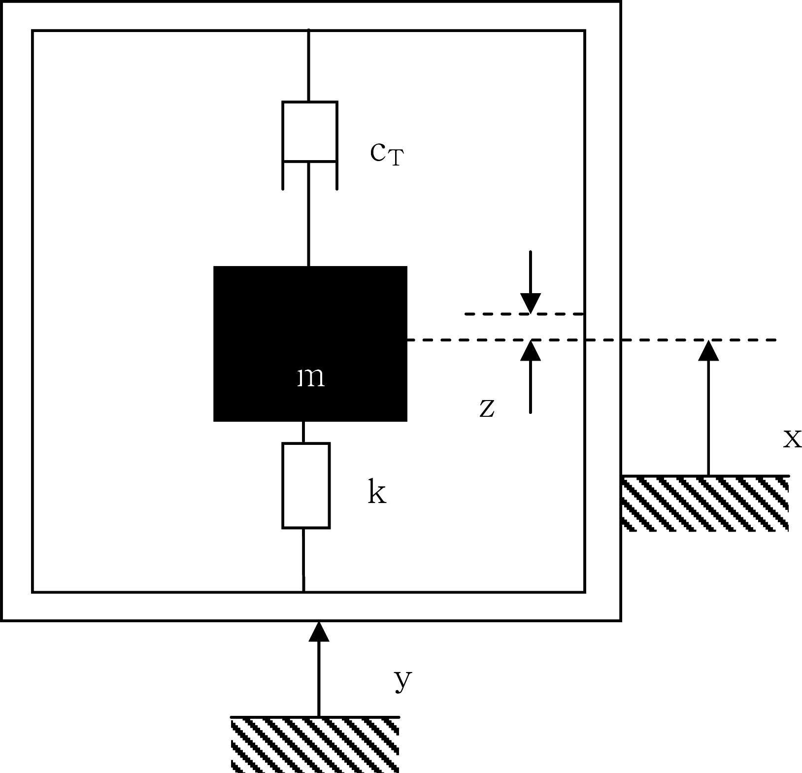
2. Vibration Energy Harvesting
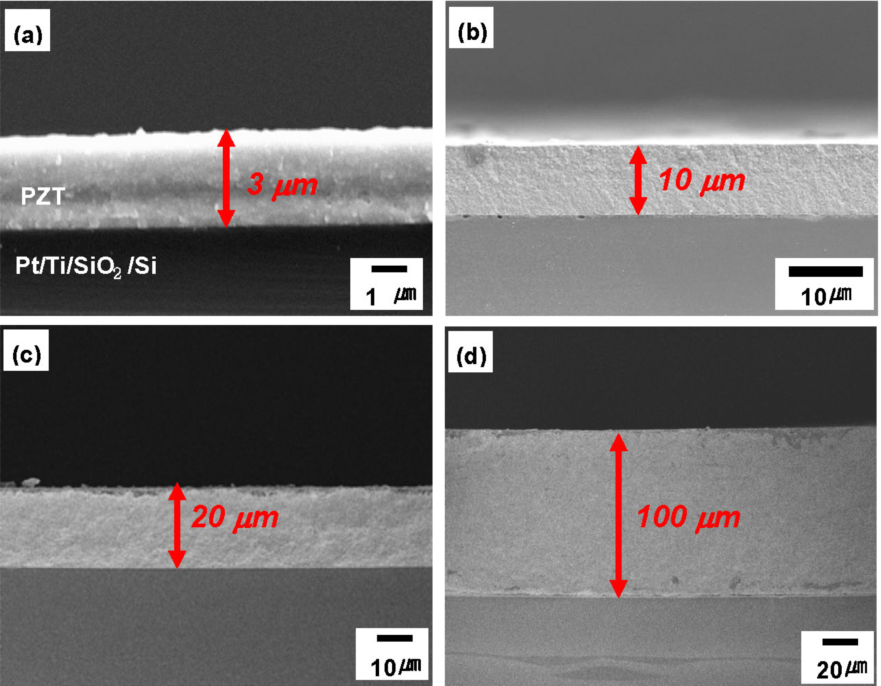
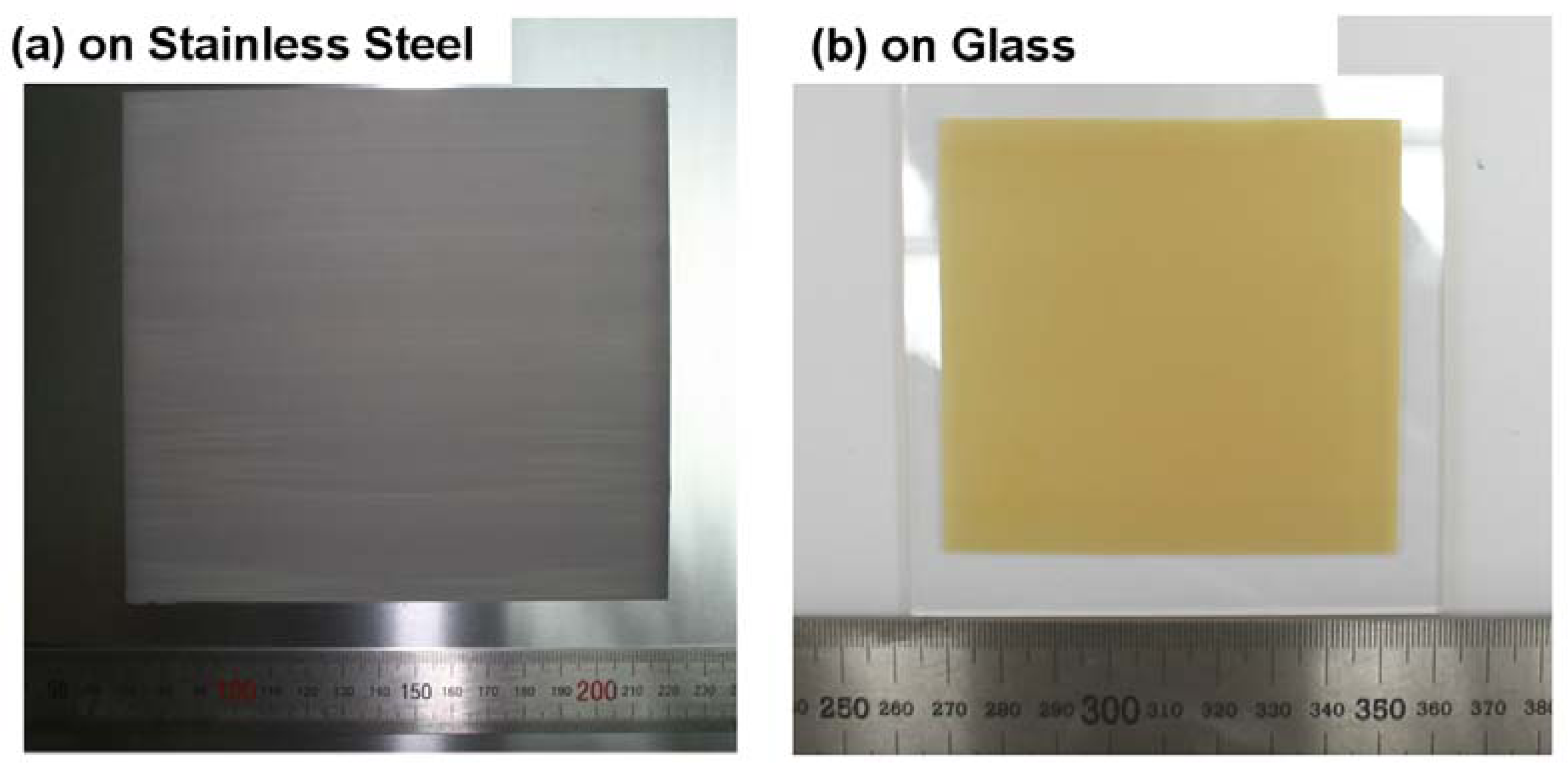
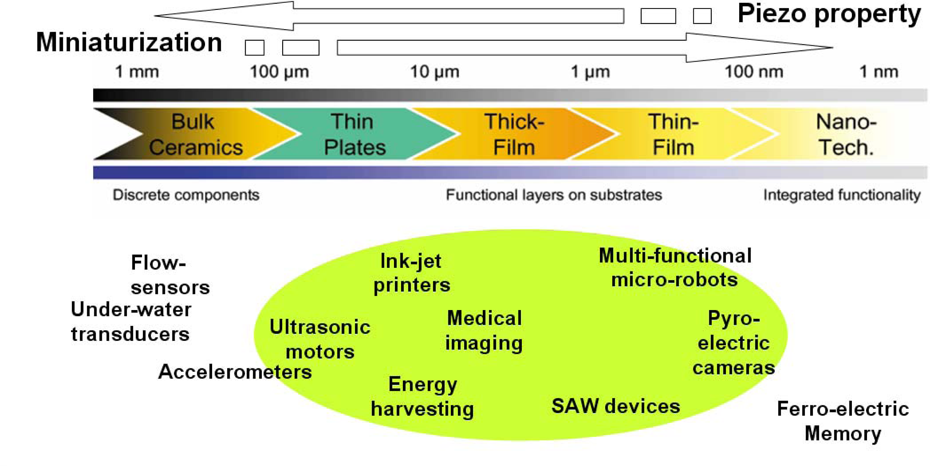
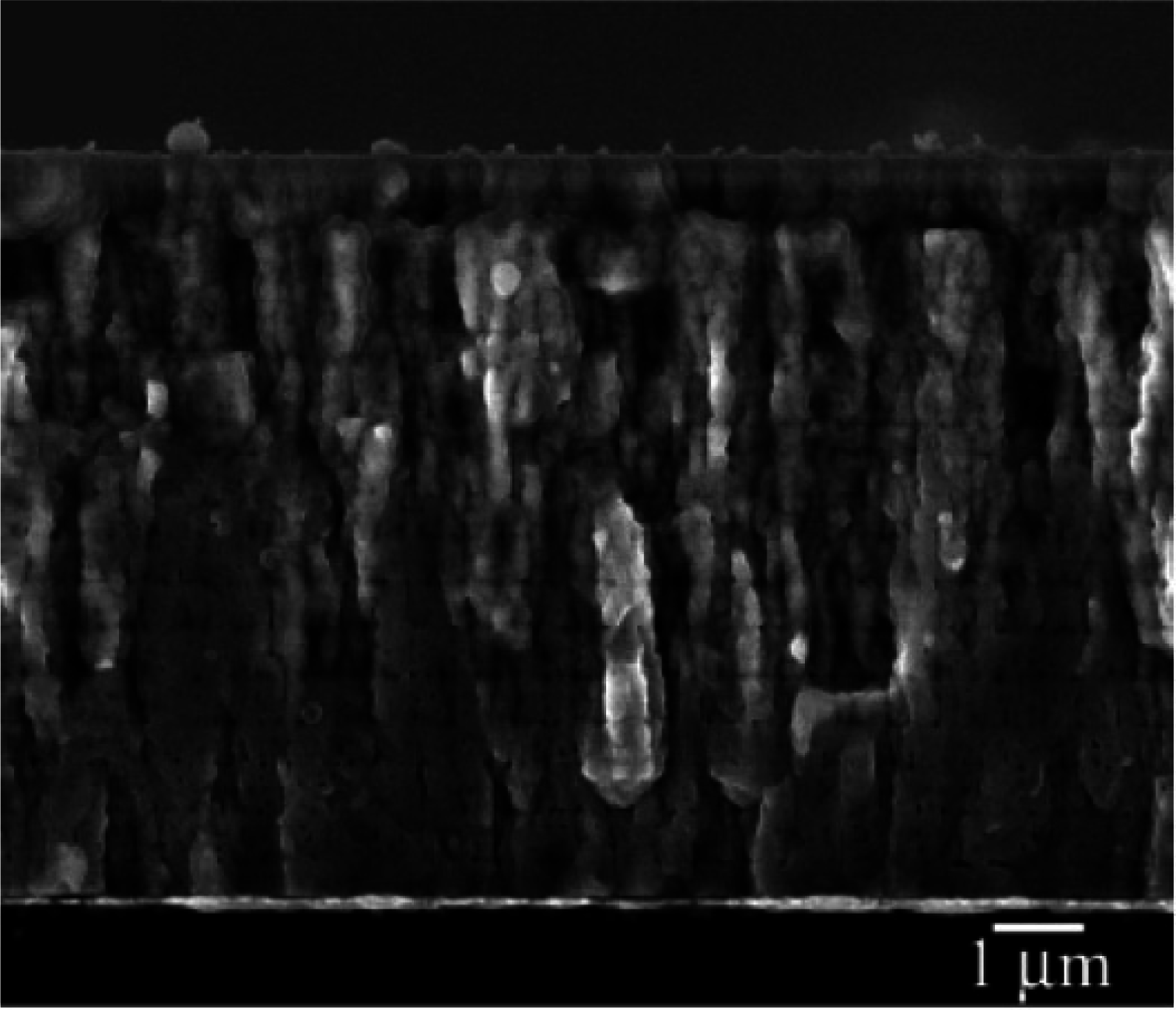
3. Piezoelectric Thick Films for Energy Harvesting
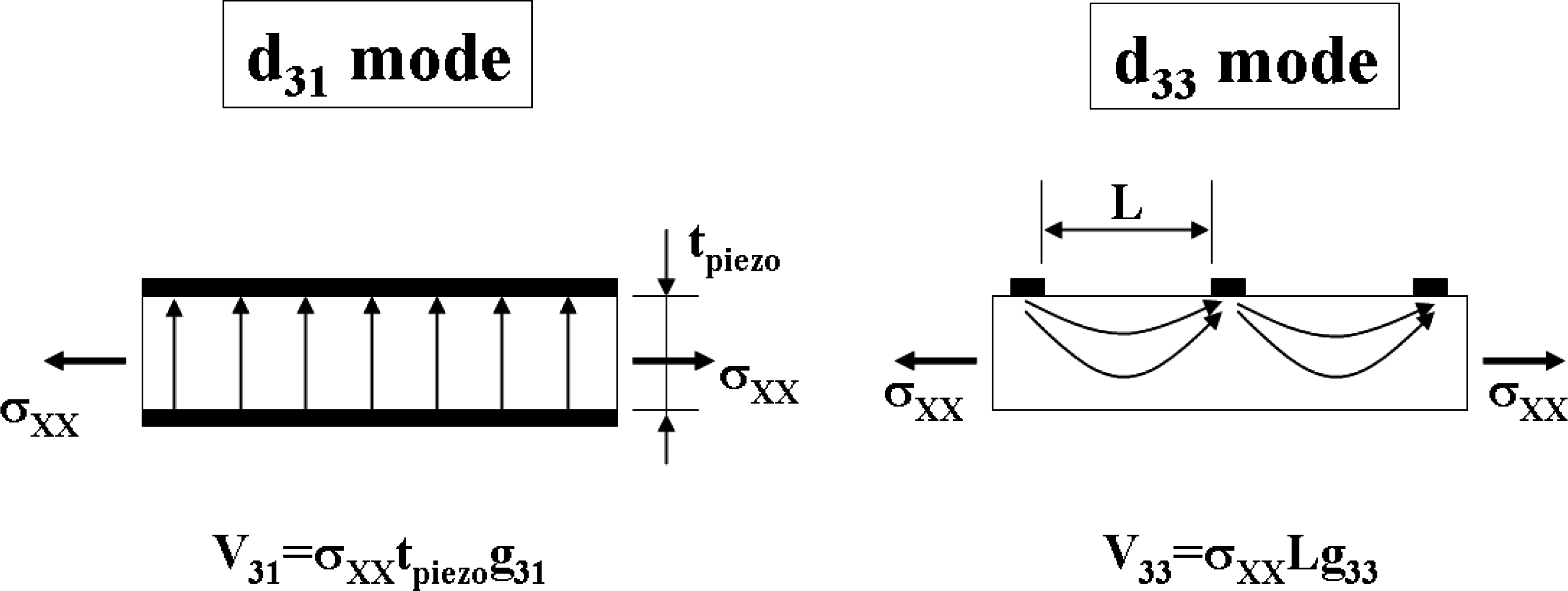
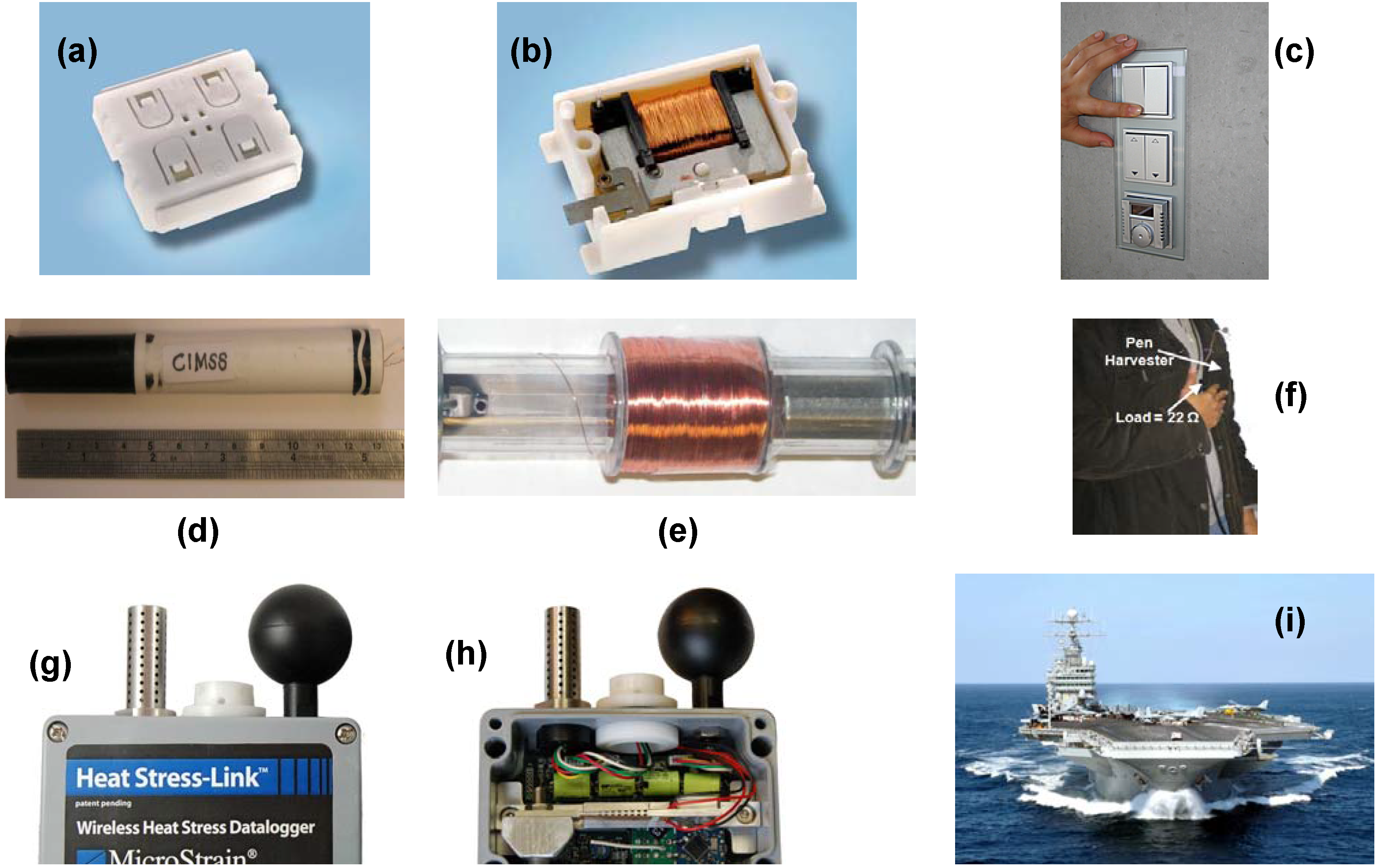
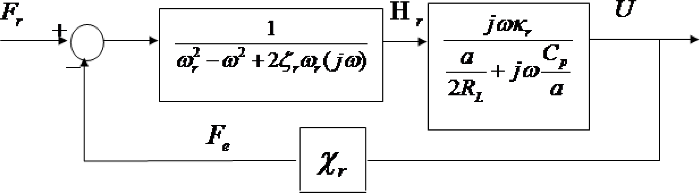
3.1. Piezoelectric Micro-Generators for Wireless Sensor Nodes
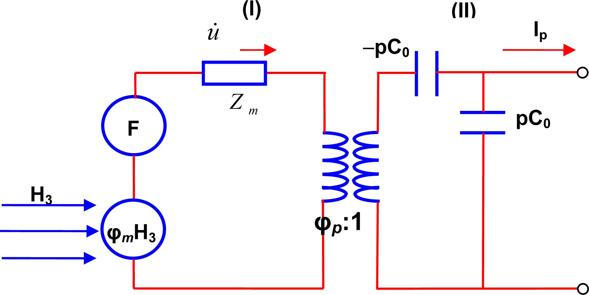
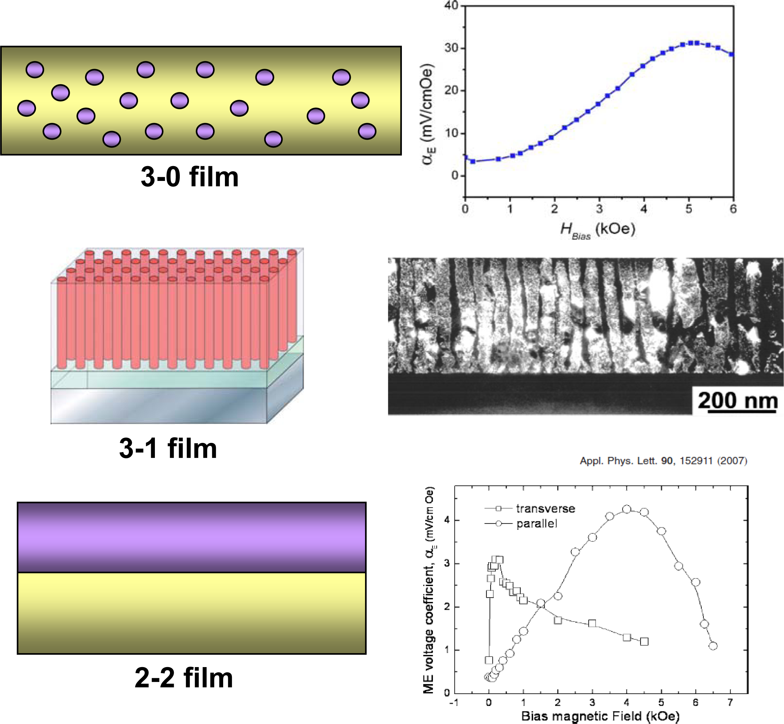
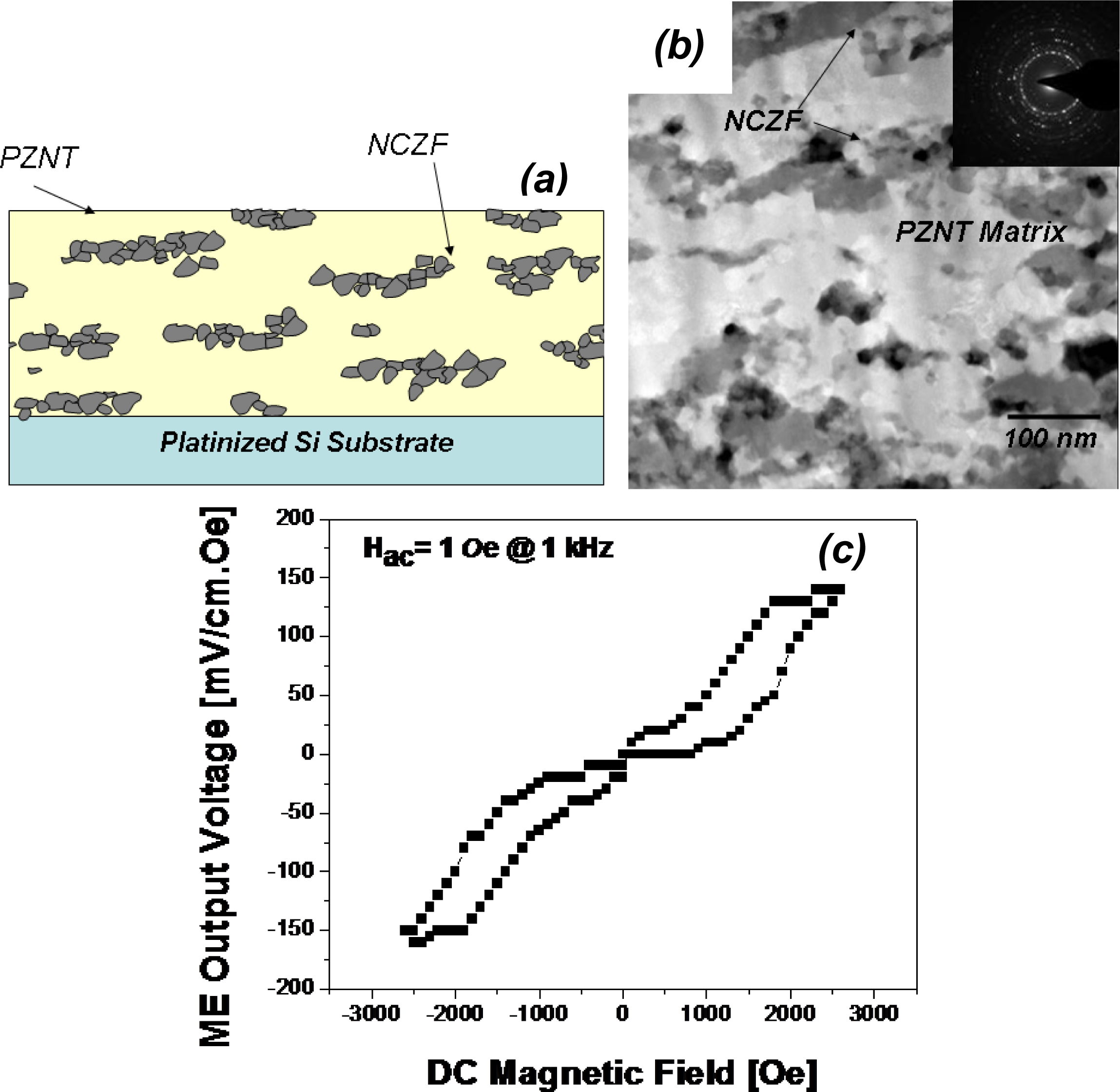
4. Magnetoelectric Composites: Thick and Thin Film
5. Conclusions
Acknowledgments
References
- Murray, C.J. Energy Harvesting Gets Real. Design News. October 2008. Available at: http://www.designnews.com/article/189768-Energy_Harvesting_Gets_Real.php (accessed March 16, 2009).
- Rabaey, J.M.; Ammer, M.J.; da Silva, J.L., Jr.; Patel, D.; Roundy, S. PicoRadio Supports ad Hoc Ultra-Low Power Wireless Networking. Computer 2000, 33, 42–48. [Google Scholar]
- Gates, B. The disappearing computer. In The World in 2003; The Economist Group: New York, NY, USA, 2002. [Google Scholar]
- Hitachi Unveils Smallest RFID Chip. RFID J. 14 March 2003. Available at: http://www.rfidjournal.com/article/view/337/1/1 (accessed August 11, 2009).
- Douseki, T.; Shigematsu, S.; Tanabe, Y.; Harada, M.; Inokawa, H.; Tsuchiya, T. A 0.5 V SIMOX-MTCMOS Circuit with 200 ps Logic Gate. Solid-State Circuits Conference, Digest of Technical Papers. 42nd ISSCC., 1996 IEEE International, San Francisco, CA, USA, February 1996; pp. 84–85.
- Jones, C.E.; Sivalingam, K.M.; Agrawal, P.; Chen, J.C. A Survey of Energy Efficient Network Protocols for Wireless Networks. Wirel. Netw 2001, 7, 343–358. [Google Scholar]
- Roundy, S.; Wright, P.K.; Rabaey, J.M. Energy Scavenging for Wireless Sensor Networks; Kluwer Academic Publishers: Boston, MA, USA, October 2004. [Google Scholar]
- Calaway, E.H., Jr. Wireless Sensor Networks; IEEE Press: New York, NY, USA, 2004. [Google Scholar]
- Energy Harvesting Technologies; Priya, S.; Inman, D.J. (Eds.) Springer Science+Business Media Inc: Norwell, MA, USA, 2008.
- Anton, S.R.; Sodano, H.A. A Review of Power Harvesting Using Piezoelectric Materials (2003–2006). Smart Mater. Struct 2007, 16, R1–R21. [Google Scholar]
- Sodano, H.A.; Inman, D.J.; Park, G. A Review of Power Harvesting from Vibration Using Piezoelectric Materials. Shock Vibration Digest 2004, 36, 197–205. [Google Scholar]
- Bedekar, V.; Oliver, J.; Priya, S. Pen Harvester for Powering a Pulse Rate Sensor. J. Phys. D–Appl. Phys 2009, 42, 105105:1–105105:9. [Google Scholar]
- Cost-Effective Packaging Solutions for Automotive Electronics. http://www.astri.org/en/techprogram/mpt/mpt02_apt05.pdf (accessed August 11, 2009).
- Sham, I. Intro of ASTRI & Energy Harvesting Solutions for Electronic Products. Presentation at IDTechEx Energy Harvesting and Storage Conference, Cambridge, UK, June 3–4, 2009.
- Erturk, A.; Inman, D.J. An Experimentally Validated Bimorph Cantilever Model for Piezoelectric Energy Harvesting from Cantilevered Beams. Smart Mater. Struct 2008, 18, 025009:1–025009:18. [Google Scholar]
- Dong, S.; Zhai, J.; Li, J.F.; Viehland, D.; Priya, S. Multimodal System for Harvesting Magnetic and Mechanical Energy. Appl. Phys. Lett 2008, 93, 103511:1–103511:18. [Google Scholar]
- Scott, J.F.; Paz De Araujo, C.A. Ferroelectric Memories. Science 1989, 246, 1400–1405. [Google Scholar]
- Paz De Araujo, C.A.; Cuchiaro, J.D.; McMillan, L.D.; Scott, M.C.; Scott, J.F. Fatigue-Free Ferroelectric Capacitors with Platinum Electrodes. Nature 1995, 374, 627–629. [Google Scholar]
- Yamakawa, K.; Imai, K.; Arisumi, O.; Arikado, T.; Yoshioka, M.; Owada, T.; Okumura, K. Novel Pb(Ti,Zr)O3 (PZT) Crystallization Technique Using Flash Lamp for Ferroelectric RAM (FeRAM) Embedded LSIs and One Transistor Type FeRAM Devices. Jpn. J. Appl. Phys 2002, 41, 2630–2634. [Google Scholar]
- Baik, S.; Setter, N.; Auciello, O. Preface: Science of Ferroelectric Thin Films and Application to Devices. J. Appl. Phys 2006, 100, 051501:0–051501:1. [Google Scholar]
- Nam, H.-J.; Kim, Y.-S.; Cho, S.-M.; Lee, C.S.; Bu, J.-U.; Hong, J.-W.; Khim, Z.-G. Calibration of Non Linear Properties of Pb(Zr,Ti)O3 Cantilever Using Integrated Piezoresistive Sensor for High Speed Atomic Force Microscopy. Jpn. J. Appl. Phys 2002, 41, 7153–157. [Google Scholar]
- Polla, D.L.; Francis, L.F. Ferroelectric Thin Films in Microelectromechanical Systems Applications. MRS Bull 1996, 21, 59–65. [Google Scholar]
- Spearing, S.M. Materials Issues in Microelectromechanical Systems (MEMS). Acta Mater 2000, 48, 179–196. [Google Scholar]
- Jeon, Y.B.; Sood, R.; Jeong, J.-H; Kim, S.-G. MEMS Power Generator with Transverse Mode Thin Film PZT. Sens. Actuat A 2005, 122, 16–22. [Google Scholar]
- Shen, D.; Park, J.-H.; Ajitasria, J.; Choe, S.-Y.; Wikle, H.C., III; Kim, D.-J. The Design, Fabrication and Evaluation of a MEMS PZT Cantilever with an Intergrated Si Proof Mass for Vibration Energy Harvesting. J. Micromech. Microeng 2008, 18, 055017:1–055017:7. [Google Scholar]
- Evans, A.G.; Hutchison, J.W. The Thermomechanical Integrity of Thin Films and Multilayers. Acta Metall. Mater 1995, 43, 2507–2530. [Google Scholar]
- Zhou, Y.C.; Yang, Z.Y.; Zheng, X.J. Residual Stress in PZT Thin Films Prepared by Pulsed Laser Deposition. Surf. Coat. Tech 2003, 162, 202–211. [Google Scholar]
- Park, S.-E.; Shrout, T.R. Ultrahigh Strain and Piezoelectric Behavior in Relaxor Based Ferroelectric Single Crystals. J. Appl. Phys 1997, 82, 1804–1811. [Google Scholar]
- Du, X.; Belegundu, U.; Uchino, K. Crystal Orientation Dependence of Piezoelectric Properties in Lead Zirconate Titanate: Theoretical Expectation for Thin Films. Jpn. J. Appl. Phys 1997, 36, 5580–5587. [Google Scholar]
- Du, X.; Zheng, J.; Belegundu, U.; Uchino, K. Crystal Orientation Dependence of Piezoelectric Properties of Lead Zirconate Titanate Near the Morphotropic Phase Boundary. Appl. Phys. Lett 1998, 72, 2421–2423. [Google Scholar]
- Kalpat, S.; Du, X.; Abothu, I.R.; Akiba, A.; Goto, H.; Uchino, K. Effect of Crystal Orientation on Dielectric Properties of Lead Zirconium Titanate Thin Films Prepared by Reactive RF-Sputtering. Jpn. J. Appl. Phys 2001, 40, 713–717. [Google Scholar]
- Chen, S.-Y.; Chen, I.-W. Temperature-Time Texture Transition of Pb(Zr1-xTix)O3 Thin Films: I, Role of Pb-rich Intermediate Phase. J. Am. Ceram. Soc 1994, 77, 2332–2336. [Google Scholar]
- Chen, S.-Y.; Chen, I.-W. Temperature-Time Texture Transition of Pb(Zr1-xTix)O3 Thin Films: II, Heat Treatment and Compositional Effects. J. Am. Ceram. Soc 1994, 77, 2337–2344. [Google Scholar]
- Chen, S.Y.; Sun, C.L. Ferroelectric Characteristics of Oriented Pb(Zr1-xTix)O3 films. J. Appl. Phys 2001, 90, 2970–2974. [Google Scholar]
- Taylor, D.V.; Damjanovic, D. Piezoelectric Properties of Rhombohedral Pb(Zr,Ti)O3 Thin Films with (100), (111), and Random Crystallographic Orientation. Appl. Phys. Lett 2000, 76, 1615–1617. [Google Scholar]
- Shimizu, M.; Okaniwa, M.; Fujisawa, H.; Niu, H. Crystalline and Ferroelectric Properties of Pb(Zr,Ti)O3 Thin Films Grown by Low-Temperature Metalorganic Chemical Vapor Deposition. Jpn. J. Appl. Phys 2002, 41, 6686–6689. [Google Scholar]
- Brooks, K.G.; Reaney, I.M.; Klissurska, R.; Huang, Y.; Bursill, L.; Setter, N. Orientation of Rapid Thermally Annealed Lead Zirconate Titanate Thin Films on (111) Pt Substrates. J. Mater. Res 1994, 9, 2540–2553. [Google Scholar]
- Krupanidhi, S.B.; Maffei, N.; Sayer, M.; El-Assal, K. Rf Planar Magnetron Sputtering and Characterization of Ferroelectric Pb(Zr,Ti)O3 Films. J. Appl. Phys 1983, 54, 6601–6609. [Google Scholar]
- Hau, S.K.; Wong, K.H.; Chan, P.W.; Choi, C.L. Intrinsic Resputtering in Pulsed-Laser Deposition of Lead-Zirconate-Titanate Thin Films. Appl. Phys. Lett 1995, 66, 245–247. [Google Scholar]
- Wang, Z.J.; Kikuchi, K.; Maeda, R. Effect of Pb contents in Target on Electrical Properties of Laser Ablation Derived Lead Zirconate Titanate Thin Films. Jpn. J. Appl. Phys 2000, 39, 5413–5417. [Google Scholar]
- Park, G.-T.; Park, C.-S.; Choi, J.-J.; Lee, J.-W.; Kim, H.-E. Effects of Thickness on Piezoelectric Properties of Highly Oriented Lead Zirconate Titanate Films. J. Am. Ceram. Soc 2006, 89, 2314–2316. [Google Scholar]
- Park, C.-S.; Lee, J.-W.; Park, G.-T.; Kim, H.-E.; Choi, J.-J. Microstructural Evolution and Piezoelectric Properties of Thick PZT Films Deposited by Multi-Sputtering: Part I. Microstructural Evolution. J. Mater. Res 2007, 22, 1367–1372. [Google Scholar]
- Park, C.-S.; Lee, J.-W.; Park, G.-T.; Kim, H.-E.; Choi, J.-J. Microstructural Evolution and Piezoelectric Properties of Thick PZT Films Deposited by Multi-Sputtering: Part II. Piezoelectric properties. J. Mater. Res 2007, 22, 1373–1377. [Google Scholar]
- Chen, L.; Li, J.-H.; Slutsker, J.; Ouyang, J.; Roytburd, A.L. Contribution of Substrate to Converse Piezoelectric Response of Constrained Thin Films. J. Mater. Res 2004, 19, 2853–2858. [Google Scholar]
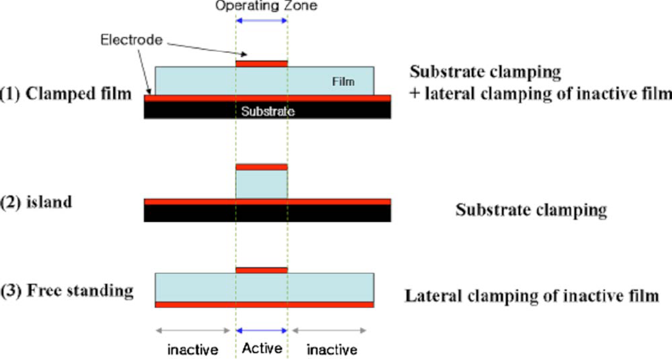
- Torah, R.N.; Beeby, S.P.; White, N.M. Experimental Investigation into the Effect of Substrate Clamping on the Piezoelectric Behavior of Thick-Film PZT Elements. J. Phys. D: Appl. Phys 2004, 37, 1074–1078. [Google Scholar]
- Gwirc, S.N.; Negreira, C.A. Evaluation of the Effect of Porosity and Substrate on the Piezoelectric Behaviour of Thick-Film PZT Element. J. Phys. D: Appl. Phys 2006, 39, 4215–4221. [Google Scholar]
- Sengupta, S.S.; Park, S.M; Payne, D.A.; Allen, L.H. Origins and Evolution of Stress Development in Sol-Gel Derived Thin Layers and Multideposited Coatings of Lead Titanate. J. Appl. Phys 1998, 83, 2291–2295. [Google Scholar]
- Ryu, J.; Priya, S.; Park, C.-S.; Kim, K.-Y.; Choi, J.-J.; Hahn, B.-D.; Yoon, W.-H.; Lee, B.-K.; Park, D.-S.; Park, C. Enhanced Domain Contribution to Ferroelectric Properties in Freestanding Thick Films. J. Appl. Phys 2009, 106, 024108:1–024108:6. [Google Scholar]
- Lebedev, M.; Akedo, J. Effect of Thickness on the Piezoelectric Properties of Lead Zirconate Titanate Films Fabricted by Aerosol Deposition Method. Jpn. J. Appl. Phys 2002, 41, 6669–6673. [Google Scholar]
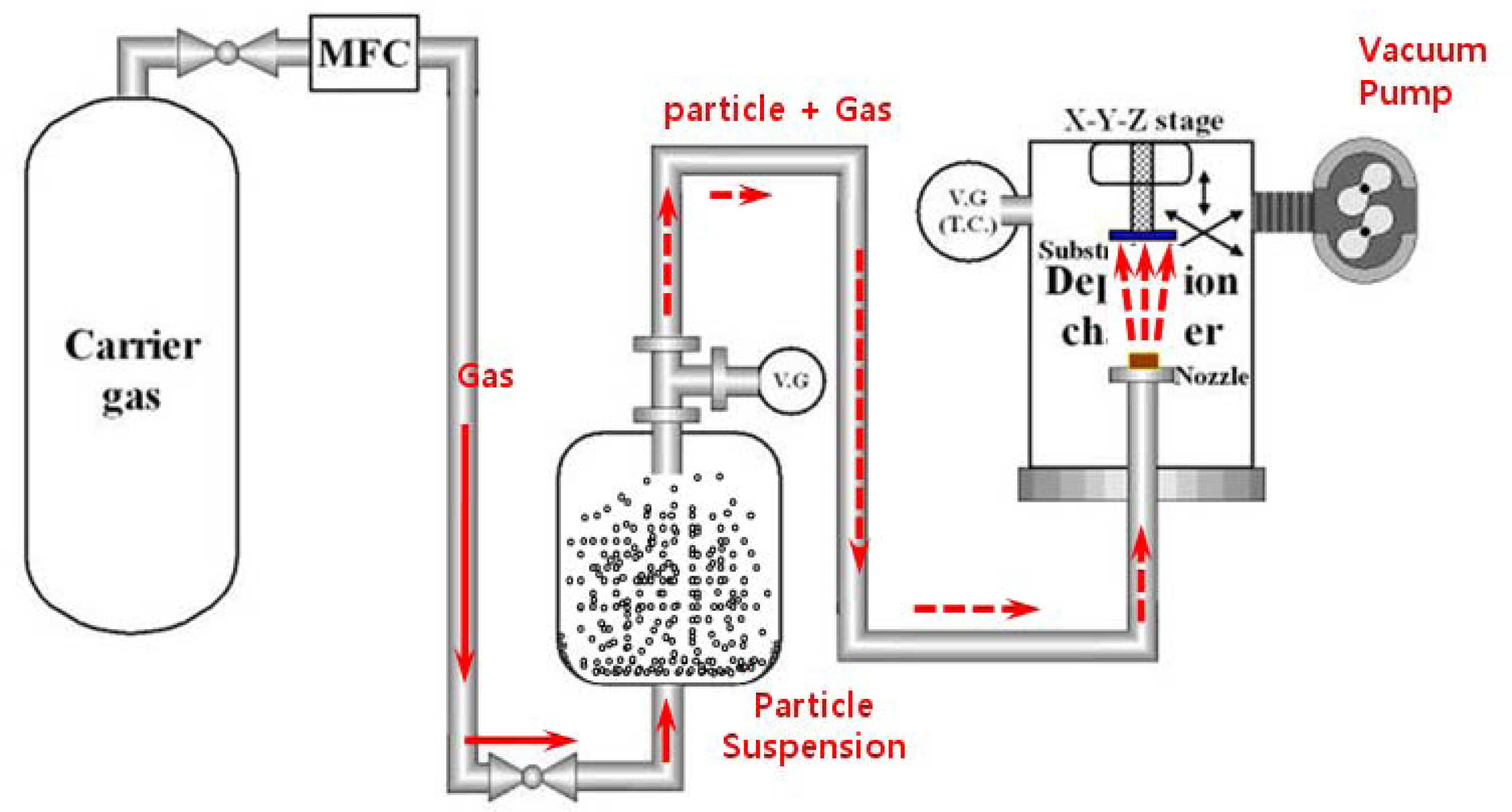
- Akedo, J. Aerosol Deposition of Ceramic Thick Films at Room Temperature: Densification Mechanism of Ceramic Layers. J. Am. Ceram. Soc 2006, 89, 1834–1839. [Google Scholar]
- Choi, J.-J.; Jang, J.-H.; Han, B.-D.; Park, D.-S.; Yoon, W.-H.; Ryu, J.; Park, C. Preparation of Highly dense PZN-PZT Thick Films by the Aerosol Deposition Method Using Excess-PbO Powder. J. Am. Ceram. Soc 2007, 90, 3389–3394. [Google Scholar]
- Ryu, J.; Choi, J.-J.; Han, B.-D.; Park, D.-S.; Yoon, W.-H.; Kim, K.-Y. Sintering and Piezoelectric Properties of KNN Ceramics Doped with KZT. IEEE Trans. Ultrason. Ferroelectr. Equation Control 2007, 54, 2510–2595. [Google Scholar]
- Ryu, J.; Choi, J.-J.; Han, B.-D.; Park, D.-S.; Yoon, W.-H.; Kim, K.-H. Fabrication and Ferroelectric Properties of High Dense Lead-Free Piezoelectric (K0.5Na0.5)NbO3 thick Films by Aerosol Deposition. Appl. Phys. Lett 2007, 90, 152901. [Google Scholar]
- Han, B.-D. Piezoelectric Thick Films. Ph.D Thesis,. Seoul National University, Seoul, Korea, 2008. [Google Scholar]
- Zhang, Q.; Whatmore, R.R. Hysteretic Properties of Mn-Doped Pb(Zr,Ti)O3 Thin Films. J. Euro. Ceram. Soc 2004, 24, 277–282. [Google Scholar]
- Ryu, J.; Park, C.-S.; Kim, K.-Y.; Choi, J.-J.; Park, C.; Hahn, B.-D.; Yoon, W.-H.; Lee, B.-K.; Park, D.-S.; Priya, S. Hard Piezoelectric Pb(Zr0.52Ti0.48)O3-Pb(Zn1/3Nb2/3)O3-MnO2 Thick Film by Aerosol-Deposition. Phil. Mag. Phil. Lett 2009, in press.. [Google Scholar]
- Williams, C.B.; Yates, R.B. Analysis of a Micro-Electric Generator for Microsystems. Sens. Actuat. A 1996, 52, 8–11. [Google Scholar]
- Roundy, S.; Wright, P.K.; Rabaey, J. A Study of Low Level Vibrations as a Power Source for Wireless Sensor Nodes. Comput. Commun 2003, 26, 1131–1144. [Google Scholar]
- Priya, S. Advances in Energy Harvesting Using Low Profile Piezoelectric Transducers. J. Electroceram 2007, 19, 165–182. [Google Scholar]
- Fang, H.-B.; Liu, J.-Q.; Xu, Z.-Y.; Dong, L.; Wang, L.; Chen, D.; Cai, B.-C.; Liu, Y. Fabrication and Performance of MEMS-Based Piezoelectric Power Generator for Vibration Energy Harvesting. Microelectron. J 2006, 37, 1280–1284. [Google Scholar]
- Liu, J.-Q.; Fang, H.-B.; Xu, Z.-Y.; Mao, X.-H.; Shen, X.-C.; Chen, D.; Liao, H.; Cai, B.-C. A MEMS-Based Piezoelectric Power Generator Array for Vibration Energy Harvesting. Microelectron. J 2008, 39, 802–806. [Google Scholar]
- Renaud, M.; Karakya, K.; Sterken, T.; Fiorini, P.; Hoof, C.V.; Puers, R. Fabrication, Modelling and Characterization of MEMS Piezoelectric Vibration Harvesters. Sens. Actuat. A 2008, 145–146, 380–386. [Google Scholar]
- Marzencki, M.; Ammar, Y.; Basrour, S. Integrated Powder Harvesting System Including a MEMS Generator and a Power Management Circuit. Sens. Actuat. A 2008, 145–146, 363–370. [Google Scholar]
- Xu, B.; Ye, Y.; Cross, L.E.; Bernstein, J.J.; Miller, R. Dielectric Hysteresis from Transverse Electric Fields in Lead Zirconate Titanate Thin Films. Appl. Phys. Lett 1999, 74, 3549–3551. [Google Scholar]
- Choi, W.J.; Jeon, Y.; Jeong, J.-H.; Sood, R.; Kim, S.G. Energy Harvesting MEMS Device Based on Thin Film Piezoelectric Cantilevers. J. Electroceram 2006, 17, 543–548. [Google Scholar]
- Curie, P. Sur la Symétrie dans les Phénomènes Physiques. J. Phys 1894, 3ed Ser.,. 393–415. [Google Scholar]
- O’Dell, T.H. Magnetoelectrics- A New Class of Materials. Electron. Power 1965, 11, 266–267. [Google Scholar]
- Ryu, J.; Carazo, A.V.; Uchino, K.; Kim, H.-E. Magnetoelectric Properties in Piezoelectric and Magnetostrictive Laminar Composites. Jpn. J. Appl. Phys 2001, 40, 4948–4951. [Google Scholar]
- Ryu, J.; Priya, S.; Uchino, K.; Kim, H.-E. Magnetoelectric Effect in Composites of Magnetostrictive and Piezoelectric Materials. J. Electroceram 2002, 8, 107–120. [Google Scholar]
- Suchetelene, J.V. Product Properties: A New Application of Composite Materials. Philips Res. Report 1972, 27, 28–37. [Google Scholar]
- Newnham, R.E.; Skinner, D.P.; Cross, L.E. Connectivity and Piezoelectric-Pyroelectric Composites. Mat. Res. Bull 1978, 13, 525–536. [Google Scholar]
- Kim, H.; Lee, W.-H.; Dias, R.; Priya, S. Piezoelectric Microgenerator-Current Status, and Challenges. IEEE Trans. Ultrason. Ferroelectr. FrEquation Control 2009. in print.. [Google Scholar]
- Zheng, H.; Wang, J.; Lofland, S.E.; Ma, Z.; Mohaddes-Ardabili, L.; Zhao, T.; Salamanca-Riba, L.; Shinde, S.R.; Ogale, S.B.; Bai, F.; Viehland, D.; Jia, Y.; Schlom, D.G.; Wuttig, M.; Roytburd, A.; Ramesh, R. Multiferroic BaTiO3-CoFe2O4 Nanostructures. Science 2004, 303, 661–663. [Google Scholar]
- Zheng, H.; Wang, J.; Mohaddes-Ardabili, L.; Wuttig, M.; Salamanca-Riba, L.; Schlom, D.G.; Ramesh, R. Three-Dimensional Hetetoepitaxy in Self-Assmbled BaTiO3-CoFe2O4 Nanostructures. Appl. Phys. Lett 2004, 85, 2035–2037. [Google Scholar]
- Zavaliche, F.; Zheng, H.; Mohaddes-Ardabili, L.; Yang, S.Y.; Zhan, Q.; Shafer, P.; Reilly, E.; Chopdekar, R.; Jia, Y.; Wright, P.; Schlom, D.G.; Suzuki, Y.; Ramesh, R. Electric Field-Induced Magnetization Switching in Epitaxial Columnar Nanostructures. Nano Lett 2005, 5, 1793–1796. [Google Scholar]
- Wan, J.G.; Zhang, H.; Wang, X.; Pan, D.; Liu, J.-M.; Wang, G. Magnetoelectric CoFe2O4-Lead Zirconate Titanate Thick Films Prepared by a Polyvinylpyrrolidone-Assisted Sol-Gel Method. Appl. Phys. Lett 2006, 89, 122914:1–122914:3. [Google Scholar]
- Ryu, H.; Murugavel, P.; Lee, J.H.; Chae, S.C.; Noh, T.W.; Oh, Y.S.; Kim, H. J.; Kim, K. H.; Bae, C.; Park, J.-G. Magnetoelectric Effects of Nanopartiulate Pb(Zr0.52Ti0.48)O3-NiFe2O4 Composite Films. Appl. Phys. Lett 2006, 89, 102907:1–102907:3. [Google Scholar]
- Zhou, J.-P.; He, H.; Shi, Z.; Nan, C.-W. Magnetoelectric CoFe2O4/Pb(Zr0.52Ti0.48)O3 Double-Layer Thin Film Prepared by Pulsed-Laser Deposition. Appl. Phys. Lett 2006, 88, 013111:1–013111:3. [Google Scholar]
- Ma, Y.G.; Cheng, W.N.; Ning, M.; Ong, C.K. Magnetoelectric Effect in Epitaxial Pb(Zr0.52Ti0.48)O3/La0.7Sr0.3MnO3 Composite Thin Film. Appl. Phys. Lett 2007, 90, 152911:1–152911:3. [Google Scholar]
- Park, C.-S.; Ryu, J.; Choi, J.-J.; Park, D.-S.; Ahn, C.-W.; Priya, S. Giant Magnetoelectric Coefficient in 3-2 Nanocomposite Thick Films. Jpn. J. Appl. Phys 2009, 48, 080204:1–080204:3. [Google Scholar]


| Human body | Vehicles | Structures | Industrial | Environment |
|---|---|---|---|---|
| Breathing, blood pressure, exhalation, body heat, walking, arm motion, finger motion, jogging, swimming, eating, talking | Aircraft, UAV, helicopter, automobiles, trains, tires, tracks, peddles, brakes, shock absorbers, turbines | Bridges, roads, tunnels, farm house structures, control-switch, HVAC systems, ducts, cleaners, etc. | Motors, compressors, chillers, pumps, fans, conveyors, cutting and dicing, vibrating mach. | Wind, ocean currents, acoustic waves. |
| Power (μW) | Frequency (Hz) | Acceleration (g) | Power density (μW/cm3) | Mode | Materials | Ref. |
|---|---|---|---|---|---|---|
| 1.0 | 13.9k | 10.8 | 37,037* | d33 | PZT | [24] |
| 2.16 | 609 | 1 | 10,843* | d31 | PZT | [60] |
| 2.15 | 461 | 2 | 3,272 | d31 | PZT | [25] |
| 3.98 | 226–234 | 0.5 | ------ | d31 | PZT | [61] |
| 40 | 1.8k | 1.9* | 21,680* | d31 | PZT | [62] |
| 0.045 | 1,495 | 2 | ------- | d31 | AIN | [63] |
© 2009 by the authors; licensee MDPI, Basel, Switzerland This article is an open access article distributed under the terms and conditions of the Creative Commons Attribution license (http://creativecommons.org/licenses/by/3.0/).
Share and Cite
Priya, S.; Ryu, J.; Park, C.-S.; Oliver, J.; Choi, J.-J.; Park, D.-S. Piezoelectric and Magnetoelectric Thick Films for Fabricating Power Sources in Wireless Sensor Nodes. Sensors 2009, 9, 6362-6384. https://doi.org/10.3390/s90806362
Priya S, Ryu J, Park C-S, Oliver J, Choi J-J, Park D-S. Piezoelectric and Magnetoelectric Thick Films for Fabricating Power Sources in Wireless Sensor Nodes. Sensors. 2009; 9(8):6362-6384. https://doi.org/10.3390/s90806362
Chicago/Turabian StylePriya, Shashank, Jungho Ryu, Chee-Sung Park, Josiah Oliver, Jong-Jin Choi, and Dong-Soo Park. 2009. "Piezoelectric and Magnetoelectric Thick Films for Fabricating Power Sources in Wireless Sensor Nodes" Sensors 9, no. 8: 6362-6384. https://doi.org/10.3390/s90806362