Article

DNA Optical Detection Based on Porous Silicon Technology: from Biosensors to Biochips

1
Institute for Microelectronics and Microsystems – Unit of Naples – National Council of Research, Via P. Castellino 111, 80131 Napoli, Italy
2
Department of Biochemistry and Medical Biotechnologies, University of Naples “Federico II”, Via S. Pansini 5, 80131 Napoli, Italy
3
Department of Organic Chemistry and Biochemistry, University of Naples “Federico II”, Via Cinthia, 80128 Napoli, Italy
4
Department of Physical Sciences, University of Naples “Federico II”, Via Cinthia, 80126 Naples, Italy
*
Author to whom correspondence should be addressed.
Sensors 2007, 7(2), 214-221; https://doi.org/10.3390/s7020214
Submission received: 15 February 2007 / Revised: 26 February 1995 / Accepted: 1 January 2007 / Published: 28 February 2007

Abstract

:
A photochemical functionalization process which passivates the porous silicon surface of optical biosensors has been optimized as a function of the thickness and the porosity of the devices. The surface modification has been characterized by contact angle measurements. Fluorescence measurements have been used to investigate the stability of the DNA single strands bound to the nanostructured material. A dose-response curve for an optical label-free biosensor in the 6-80 mM range has been realized.

1. Introduction

Biosensors are nowadays technological hot topics due to the possible applications in social interest fields such as medical diagnostic and health care, monitoring of environmental pollutants, home and defence security [1]. Besides the signal generated by the sensing device, the biosensor is constituted by the molecular recognition element and the transducer material. The molecular recognition element can be a biological molecule, such as DNA single strand, proteins, enzymes, or a biological system, such as membrane, cell, and tissues: in this way, the sensing mechanism takes advantage of the natural sensitivity and specificity of the biomolecular interactions. Optical transduction is more and more used since photonic devices could be small, lightweight and thus portable due to the integrability of all optical components. Furthermore, optical devices do not require electric contacts. Fluorescence is by far the most used optical signalling method but a wide-use sensor can not be limited by the labelling of the probe nor the analyte, since this step is not always possible [2]. Reagentless optical biosensors are monitoring devices which can detect a target analyte in a heterogeneous solution without the addition of anything than the sample. In the fields of genomics and proteomics this is a straightforward advantage since it allows real-time readouts and, thus, very high throughoutputs analysis. A label free optical biosensor can be realized by integrating the biological probe with a signalling material which directly transduces the molecular recognition event into an optical signal. Recently, lot of theoretical and experimental work, concerning the worth noting properties of nanostructured porous silicon (PSi) in chemical and biological sensing, has been reported, showing that, due to its morphological and physical properties, PSi is a very versatile sensing platform [3, 4]. PSi is an available, low cost material, completely compatible with VLSI and micromachining technologies, so that it could usefully be employed in the fabrication of micro-opto-electric-mechanical system and smart sensors. PSi is also very used as photonic material due to the possibility of fabricating high quality optical structures, either as single layers, like Fabry-Perot interferometers [5], or multilayers, such as Bragg [6] or rugate filters [7]. A key feature for a recognition transducer is a large surface area: PSi has a porous structure with a specific area up to 200 – 500 m2 cm-3, so that it can be very sensitive to the presence of biochemical species which penetrate inside the pores. Unfortunately, the surface of the “as etched” PSi is highly hydrophobic so that aqueous solution can not infiltrate the sponge like matrix. A proper passivation process must be applied to stabilise the surface and to covalently link the bioprobe [8]. The development of PSi based biosensor arrays critically depends on the surface functionalization process and how it is compatible with the microfabrication technologies. In a recently published article, we have exploited a photochemical functionalization process of the PSi surface to covalently bind DNA single strands (ssDNA) and we have also demonstrate that the device works as an all optical biosensor for ssDNA-cDNA interactions [9]. In the present work, we have optimised the functionalization process by investigating the role of thickness and porosity of the PSi chip, the time exposure to ultraviolet (UV) light and also the concentration of the ssDNA solution. Fluorescent measurements have been used to test the chip stability against the washing in aqueous solutions.

2. Experimental Section

In this study we used as optical transducer a porous silicon layer of fixed thickness and porosity: from an optical point of view, this structure acts as a Fabry-Perot interferometer. To study the influence of porous silicon physical parameters, we have fabricated several layers, obtained by electrochemical etch in a HF/EtOH (3:7) solution, at room temperature and dark light. Highly doped p+-silicon, <100> oriented, 0.005 ω cm resistivity, 400 μm thick was used. The PSi samples were characterised by variable angle spectroscopic ellipsometry [10]. Etching times and anodic current densities have been reported in Table 1.
The photo-activated chemical modification of PSi surface was based on the UV exposure of a solution of alkenes which bring some carboxylic acid groups. The PSi chip has been pre-cleaned in an ultrasonic acetone bath then washed in deionized water. After dried in N2 stream, it has been immediately covered with 10% N-hydroxysuccinimide ester (UANHS) solution in CH2Cl2. The UANHS was house synthesised as described in literature [11]. This treatment results in covalent attachment of UANHS to the porous silicon surface. The chip was then washed in dichloromethane in an ultrasonic bath for 10 min to remove any adsorbed alkene from the surface. The carboxyl-terminated monolayer covering the PSi surface works as a reactive substrate for the chemistry of the subsequent attachment of the DNA sequences. DNA single strands in a HEPES solution 10mM (pH=7.5) have been incubated overnight.
FT-IR spectroscopy (Thermo - Nicholet NEXUS) has been used to verify the efficiency of the reaction. After the chemical functionalization we have also quantitatively measured the efficiency of the binding between the DNA and the porous silicon surface using a fluorescent DNA probe (5′GGACTTGCCCGAATCTACGTGTCCA3′, Primm) labelled with a proper chromophore group (Fluorescein CY3.5, the absorption peak is at 581 nm and the emission is at 596 nm). Fluorescence images were recorded by a Leica Z16 APO fluorescence macroscopy system. The fluorescent chips have been dialyzed overnight, first in water and then in a HEPES solution, at room temperature to assess the binding between the bioprobe and the PSi surface.
Contact angle measurements have been performed by using a KSV Instruments LTD CAM 200 Optical Contact Angle Meter.
The reflectivity measurements have been performed by a very simple experimental set-up: a tungsten lamp (400 nm < λ < 1800 nm) illuminates, through an optical fiber and a collimator, the sensor and the reflected beam is collected by an objective, coupled into a multimode fiber, and then directed in an optical spectrum analyser (Ando, AQ6315A). The reflectivity spectra have been measured with a resolution of 0.5 nm.

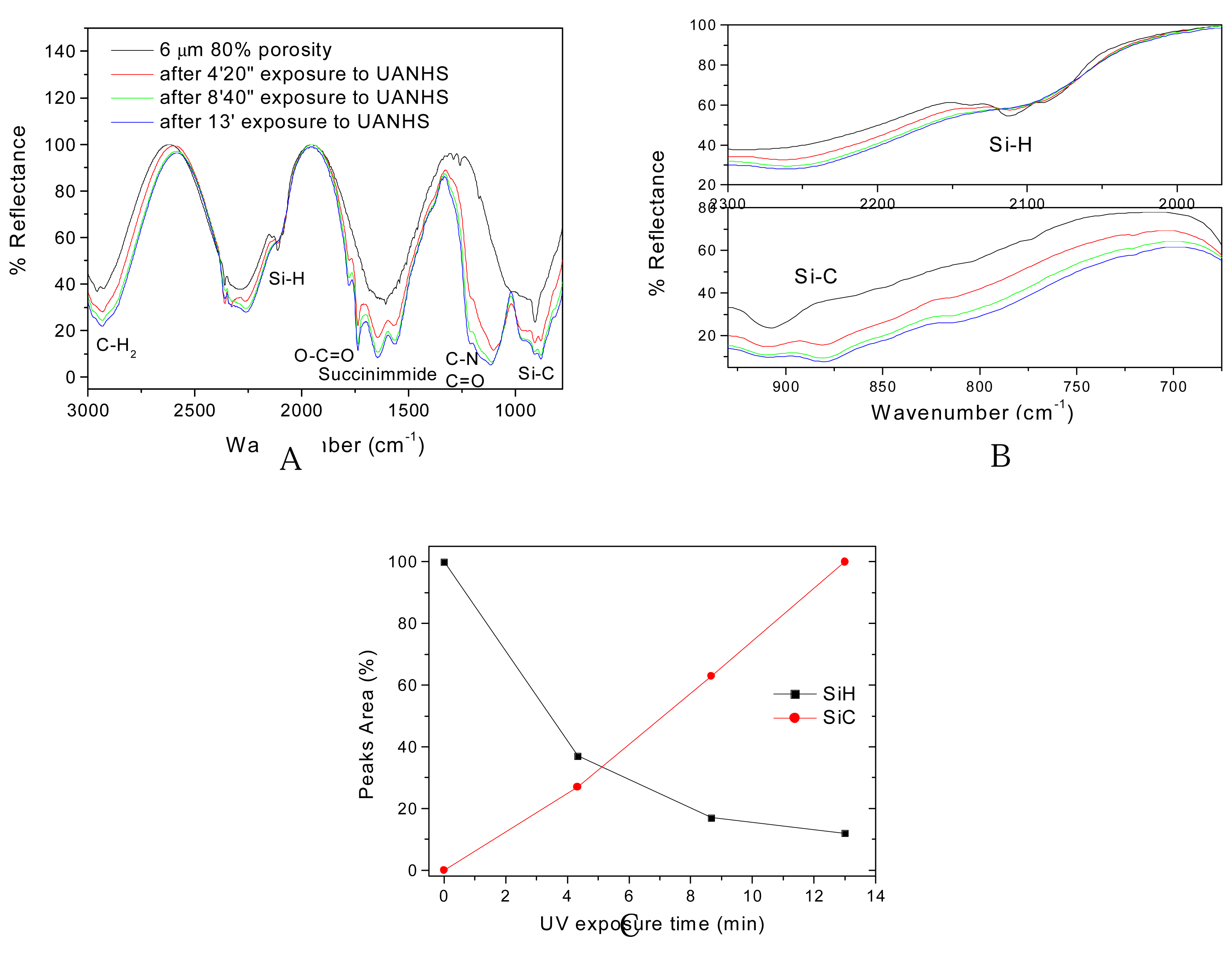
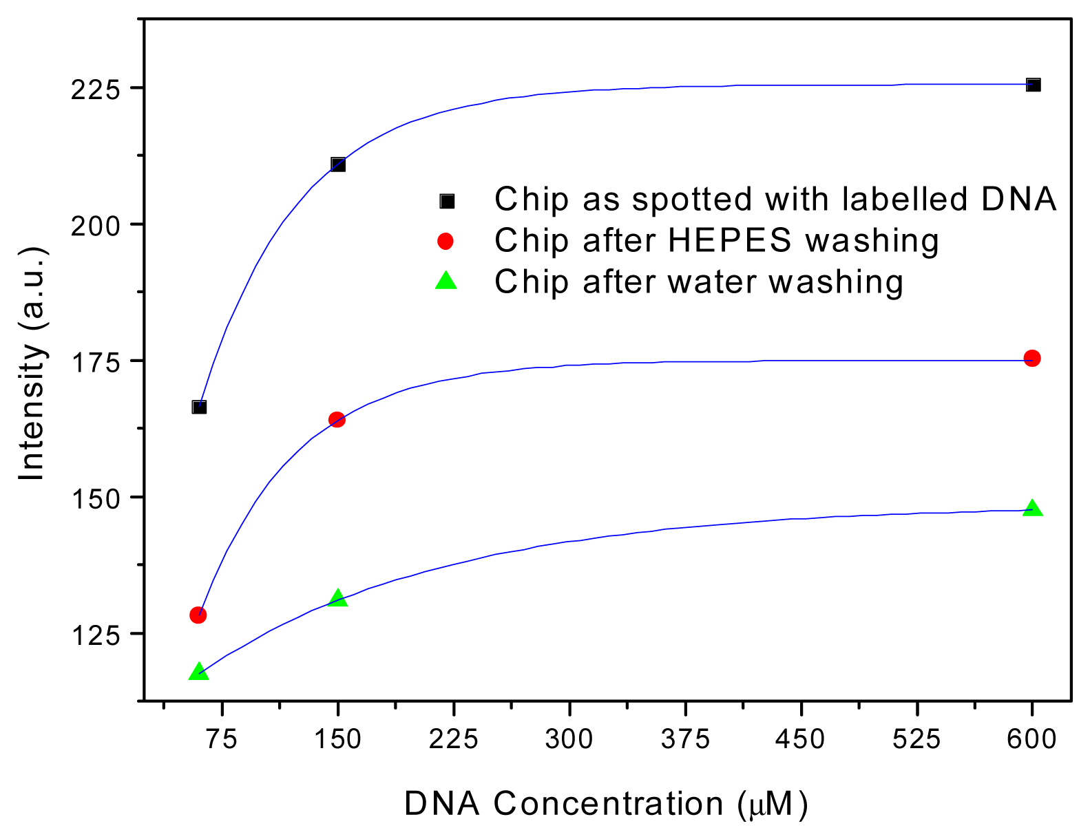
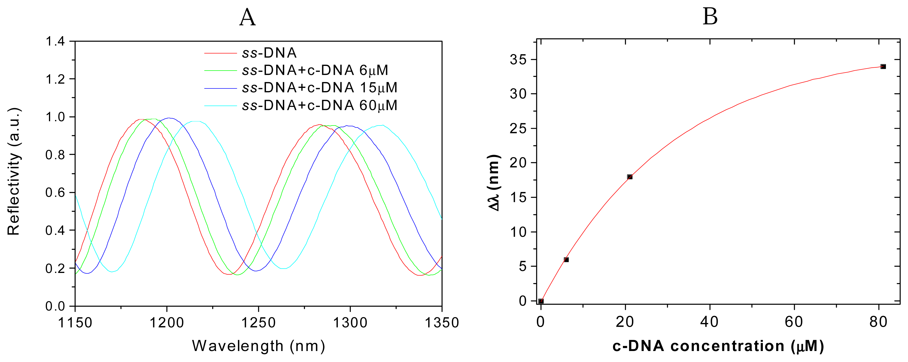
3. Results and Discussion

Infrared spectroscopy is a powerful tool in surfaces characterisation: it is fast, accurate and could also performe quantitative determinations. We have investigated all the PSi monolayers before and after the photochemical passivation process since we were worried about the functionalization efficiency of thicker samples. A thicker layer can adsorb more bioprobes than a thinner one but the UV exposure could also be less effective, due to light absorption by PSi at those frequencies. Our measurements demonstrate that up to 6 mm thick PSi monolayer, a complete passivation and functionalization of the surface can be obtained by exposing for a sufficiently long time the sample: in Figure 1A are shown the FT-IR spectra of the PSi monolayer as etched and after three different times of exposure to UV light.
The characteristic peaks of the Si-H bonds (at 2100 cm-1) progressively disappear while the amide I band (at 1634 cm-1) and the Si-C peak (at 880 cm-1) become more and more evident. Figure 1B is an enlargement of the characteristic peaks of these resonances. The reaction yield increases quite monotonically with the exposure time, as it can be seen in Figure 1C. Thinner samples can be functionalised in faster exposure times, but the overall volume available to adsorb bioprobes is drastically reduced.
The surface passivation is also well evident by contact angle measurements: the hydrogenated PSi surface is highly hydrophobic, due to the presence of the Si-H bonds, so that a drop of deionised water exploits a high surface tension which prevents its diffusion in the pores. This behaviour is well depicted in Figure 2A: the contact angle is 137±1 degree, averaging the left and right values of three different drops having the same volumes, and the estimated surface tension is 179 mN/m. After the photoreaction with the UANHS, the Si-H bonds are replaced by the Si-C bonds and the PSi surface shows a hydrophilic behaviour, as shown in Figure 2B: the drop spreads on the surface and the contact angle drastically decreases to 43±3 degree and also the surface tension is lowered to 67 mN/m. In this condition, an aqueous solution can be infiltrated in the nanostructured layer.
To test the stability of the covalent bonding between the organic linker layers, which homogeneously cover the PSi surface, and the biological probes we have used a fluorescent DNA single strand as an optical tracer. After the chemical bonding of the labelled ssDNA, the chip was observed by the fluorescence macroscopy system. Under the light of the 100W high-pressure mercury source, we have found a high and homogeneous fluorescence on the whole chip surface which still remains bright even after two overnight dialysis washings in a HEPES solution and in deionised water, as it can be seen in Figures 3 A, B, and C. We have also studied the yield of the chemical functionalization by spotting different concentrations of the fluorescent ssDNA and measuring the fluorescence intensities of the images before and after the washings. The results reported in Figure 4 confirm the qualitative findings of Figure 3: the fluorescent intensities decrease but remain of the same order of magnitude. From this graph we can also estimate the concentration of the DNA probe which saturates the binding sites available.
The PSi optical biosensors measure the change in the average refractive index of the device: when a bioconjugation event takes place, the refractive index of the molecular complex changes and the interference pattern on output is thus modified. The label free optical monitoring of the ssDNA-cDNA hybridization is simply the comparison between the optical spectra of the porous silicon layer after the UANHS and probe immobilization on the chip surface and after its hybridization with the cDNA. Each step of the chip preparation increases the optical path in the reflectivity spectrum recorded, due to the substitution of the air into the pores by the organic and biological compounds. The interaction of the ssDNA with its complementary sequence has been detected as a fringes shift in the wavelengths, which corresponds to a change in the optical path. Since the thickness d is fixed by the physical dimension of the PSi matrix, the variation is clearly due to changes in the average refractive index.
In Figure 5A the reflectivity spectra of the PSi layer for different cDNA concentration are reported, while in Figure 5B a dose-response curve is reported. A control measurement has been made using a ncDNA sequence: a very small shift (less than 2 nm) has been recorded in the reflectivity spectrum respect to the one obtained after the probe linking.
The sensor response has been fitted by a monoexponential growth model, y=A-Be-kx, where A is the offset, B the amplitude, k the rate and y'=Bk the limiting sensitivity, i.e. the sensitivity in the limit of zero ligand concentration. In this case, we obtained for this parameter the value of 1.1 (0.1) nm/μM, which corresponds to a limit of detection of 90 nM for a system able to detect a wavelength shift of 0.1 nm.
In conclusions, we have optimized the PSi surface functionalization process by investigating the role of chip thickness and porosity, on exposure to ultraviolet (UV) light for different times interval and also for different concentration of the ssDNA probe. Fluorescent measurements have confirmed the chip stability against the washing in aqueous solutions. These results will be very useful in the design and realisation of a PSi based label free optical biochip.

Acknowledgments

Authors wish to acknowledge dr. Andrea M. Rossi of National Institute of Metrological Research, Turin, Italy, for helpful discussions and Prof. N. Scaramuzza and dr. M. Giocondo of University of Calabria, Cosenza, Italy, for contact angle measurements. This work is partially supported by the FIRB Italian project RBLA033WJX_005.

References and Notes

  1. Optical Biosensors; Ligler, F.S.; Rowe Taitt, C.A. (Eds.) Elsevier: Amsterdam, The Netherlands, 2004.
  2. Salitermkan, S. S. Fundamentals of BioMEMS and Medical Microdevices; Wiley-Interscience, SPIE PRESS: Bellingham, Washington USA, 2006. [Google Scholar]
  3. Lin, V. S. Y.; Motesharei, K.; Dancil, K. P. S.; Sailor, M. J.; Ghadiri, M. R. A porous silicon-based optical interferometric biosensor. Science 1997, 278, 840–843. [Google Scholar]
  4. De Stefano, L.; Moretti, L.; Rendina, I.; Rossi, A. M. Time-resolved sensing of chemical species in porous silicon optical microcavity. Sensor and Actuators B 2004, 100, 168–172. [Google Scholar]
  5. Dancil, K. -P. S.; Greiner, D. P.; Sailor, M. J. A Porous Silicon Optical Biosensor: Detection of Reversible Binding of IgG to a Protein A-Modified Surface. J. Am. Chem. Soc. 1999, 121, 7925–7930. [Google Scholar]
  6. Snow, P. A.; Squire, E. K.; Russel, P. St. J.; Canham, L. T. Vapor sensing using the optical properties of porous silicon Bragg mirrors. J. Appl. Phys. 1999, 86, 1781–1784. [Google Scholar]
  7. Lorenzo, E.; Oton, C. J.; Capuj, N. E.; Ghulinyan, M.; Navarro-Urrios, D.; Gaburro, Z.; Pavesi, L. Porous silicon-based rugate filters. Appl. Opt. 2005, 44, 5415–5421. [Google Scholar]
  8. Ouyang, H.; Chrtistophersen, M.; Viard, R.; Miller, B. L.; Fauchet, P. M. Macroporous silicon microcavities for macromolecule detection. Adv. Funct. Mater. 2005, 15, 1851–1859. [Google Scholar]
  9. De Stefano, L.; Rotiroti, L.; Rea, I.; Rendina, I.; Moretti, L.; Di Francia, G.; Massera, E.; Lamberti, A.; Arcari, P.; Sangez, C. Porous silicon-based optical biochips. Journal of Optics A: Pure and Applied Optics 2006, 8, S540–S544. [Google Scholar]
  10. Wongmanerod, C.; Zangooie, S.; Arwin, H. Determination of pore size distribution and surface area of thin porous silicon layers by spectroscopic ellipsometry. Applied Surface Science 2001, 172, 117–125. [Google Scholar]
  11. Yin, H.B.; Brown, T.; Gref, R.; Wilkinson, J.S.; Melvin, T. Chemical modification and micropatterning of Si(100) with oligonucleotides. Microelectronic Engineering 2004, 73-74, 830–836. [Google Scholar]
Figure 1. A) FT-IR spectra of the PSi monolayer as etched and after three different times of exposure to UV light. B) Particulars of the Si-H bond and Si-C bond peaks at 2100 and 880 cm-1, respectively. C) Peaks area as function of the exposure time: the reaction yield increases monotonically with the exposure time.
Sensors 07 00214f1
Figure 2. Characterisation of the PSi surface by contact angles measurements. A) The PSi as etched shows a clearly hydrophobic behaviour. B) After the passivation process the PSi surface is hydrophilic thus allowing the penetration of biological solution.
Sensors 07 00214f2
Figure 3. A) Fluorescence of the chip surface after the binding of the labelled ssDNA; B) after the overnight dialysis in HEPES solution; C) after the overnight dialysis in deionised water.
Sensors 07 00214f3
Figure 4. Fluorescence intensities of the chip surface after the binding of the labelled ssDNA and the two overnight dialysis as a function of the cDNA concentration.
Sensors 07 00214f4
Figure 5. A) Fringes shifts due to ssDNA-cDNA interaction. B) Dose-response curve as a function of the cDNA concentration.
Sensors 07 00214f5
Table 1. PSi layers physical characteristics and fabrication parameters.
Current Density
(mA/cm2)
Porosity
(%)
Etch Rate
(nm/s)
Thickness
(μm)
Etch Time
(s)
50601932.010.4
4.020.7
6.031.1
125702472.08.1
4.016.2
6.024.3
150801372.014.6
4.029.2
6.043.8

