2.1. Hydrogen Gas Sensors based on AlGaN/GaN-Based Metal-Oxide Semiconductor Diodes
Simple GaN Schottky diodes exhibit strong changes in current upon exposure to hydrogen-containing ambients. The effect is thought to be due to a lowering of the effective barrier height as molecular hydrogen catalytically cracks on the metal gate (typically made of Pt) and atomic hydrogen diffuses to the interface between the metal and GaN, altering the interfacial charge. Eickhoff et al. [
10] found that it was necessary to have a native oxide present between the semiconductor and the gate metal in order to see significant current changes. Thus it is desirable to specifically incorporate an oxide into GaN –based diodes or HEMTs in order to maximize the hydrogen detection response.
Gas sensors based on MOS diode on AlGaN/GaN high electron mobility transistor (HEMT) layer structure are of interest, because HEMTs are expected to be the first GaN electronic device that is commercialized, as part of next generation radar and wireless communication systems. These structures have much higher sensitivity than Schottky diodes on GaN layer, because they are true transistors and therefore operate with gain. In addition, the MOS-gate version of the HEMT has significantly better thermal stability than a metal-gate structure and is well-suited to gas sensing. When exposed to changes in ambient, changes in the surface potential of the semiconductor will lead to large changes in channel current.
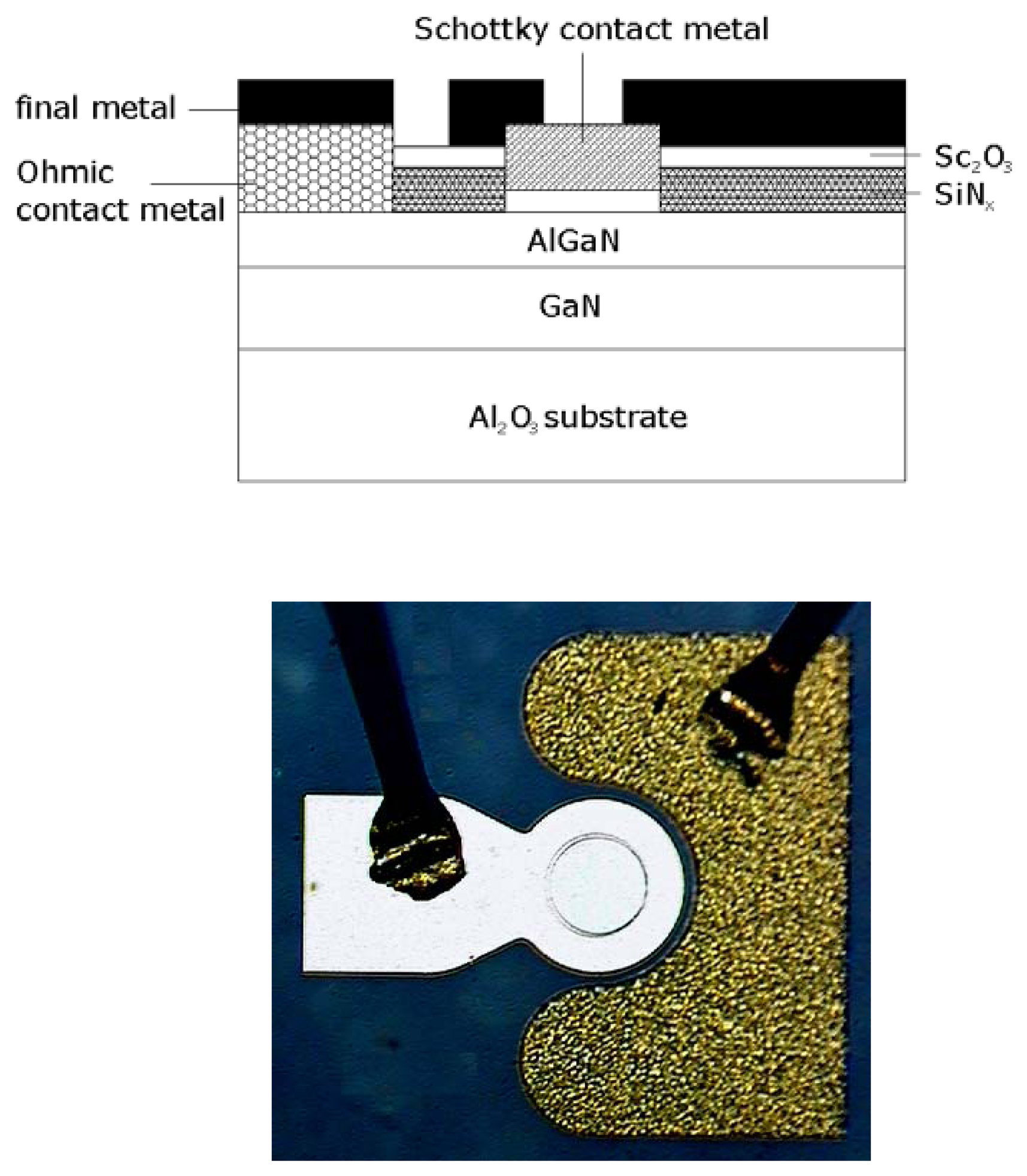
A typical HEMT gas sensor employs Ohmic contacts formed by lift-off of e-beam deposited Ti (200Å)/Al(1000Å)/Pt(400Å)/Au(800Å). The contacts are annealed at 850 °C for 45 sec to minimize the contact resistance. Thin (typically 400Å thick) gate dielectrics of MgO or Sc
2O
3 are deposited through a contact window of SiNx .The dielectrics are deposited by rf plasma-activated MBE at 100 °C using elemental Mg or Sc evaporated from a standard effusion all at 1130 °C and O
2 derived from an Oxford RF plasma source. 200 Å Pt Schottky contacts are deposited on the top of Sc
2O
3. Then, final metal of e-beam deposited Ti/Au (300Å/1200Å) interconnection contacts was employed on the MOS-HEMT diodes.
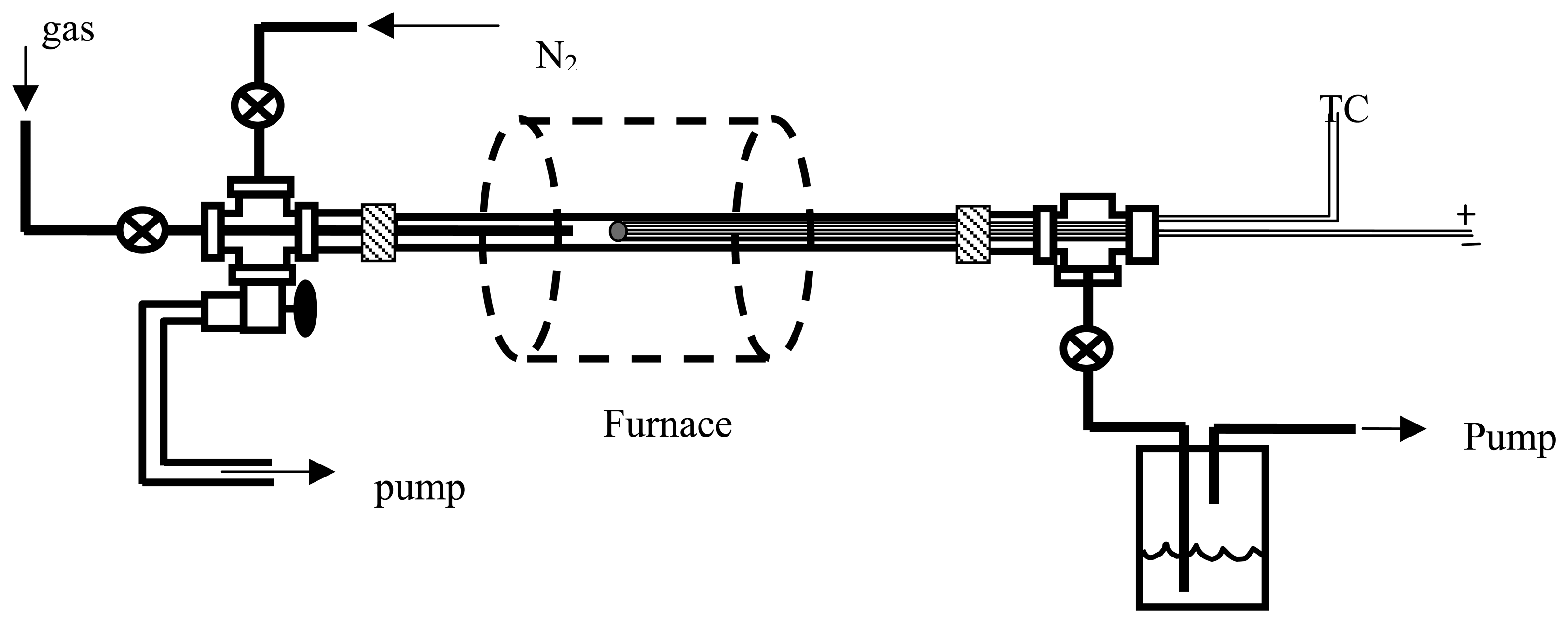
Figure 2 shows a schematic (left) and photograph (right) of the completed device. The devices are bonded to electrical feed-throughs and exposed to different gas ambients in an environmental chamber. A schematic of the chamber is shown in
Figure 3.
As the detection temperature is increased, the response of the MOS-HEMT diodes increases due to more efficient cracking of the hydrogen on the metal contact. Pt is a good choice as the contact due to its efficiency at cracking hydrogen at relatively low temperatures[
7-
10], but for applications requiring more thermally stable contacts, we have also found that W is effective at higher operating temperatures (300°C)[
16].
The threshold voltage for a MOSFET is given by [
8,
9]
where
VFB is the voltage required for flat band conditions,
фB the barrier height, e the electronic charge and
Ci the Sc
2O
3 capacitance per unit area. In analogy with results for MOS gas sensors in other materials systems, the effect of the introduction of the atomic hydrogen into the oxide is to create a dipole layer at the oxide/semiconductor interface that will screen some of the piezo-induced charge in the HEMT channel.
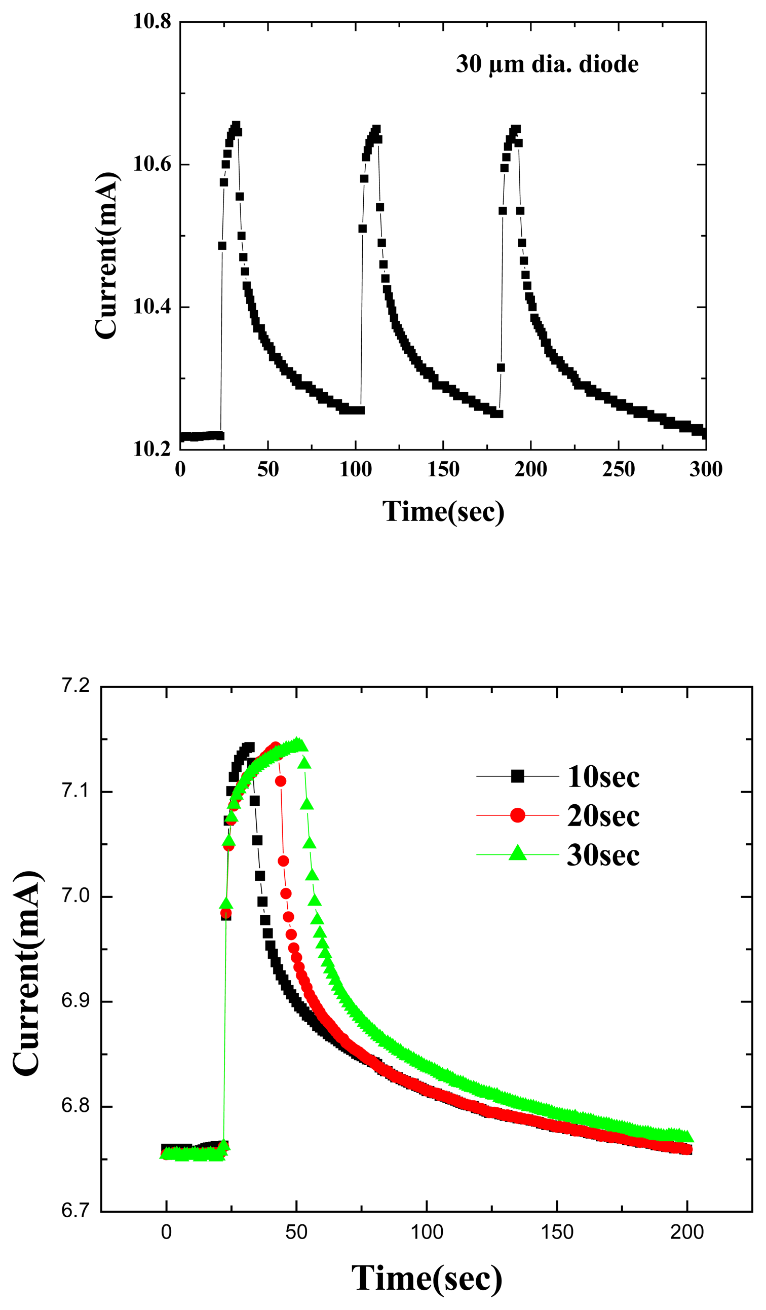
To test the time response of the MOS diode sensors, the 10%H
2/90%N
2 ambient was switched into the chamber through a mass flow controller for periods of 10, 20 or 30 seconds and then switched back to pure N
2.Figure 4 (top) shows the time dependence of forward current at a fixed bias of 2V under these conditions. The response of the sensor is rapid (<1 sec), with saturation taking almost the full 30 seconds. Upon switching out of the hydrogen–containing ambient, the forward current decays exponentially back to its initial value. This time constant is determined by the volume of the test chamber and the flow rate of the input gases and is not limited by the response of the MOS diode itself.
Figure 4 (bottom) shows the time response of the forward current at fixed bias to a series of gas injections into the chamber, of duration 10secs each (top) or 30 secs each (bottom). The MOS diode shows good repeatability in its changes of current and the ability to cycle this current in response to repeated introductions of hydrogen into the ambient. Once again, the response appears to be limited by the mass transport of gas into and out of the chamber and not to the diffusion of hydrogen through the Pt/Sc
2O
3 stack.
AlGaN/GaN MOS-HEMT diodes appear well-suited to combustion gas sensing applications. The changes in forward current are approximately double those of simple GaN Schottky diode gas sensors tested under similar conditions and suggest that integrated chips involving gas sensors and HEMT-based circuitry for off-chip communication are feasible in the AlGaN/GaN system.
2.2 Hydrogen-Induced Reversible Changes in Sc2O3/AlGaN/GaN HEMTs
Pt contacted AlGaN/GaN high electron mobility transistors with Sc
2O
3 gate dielectrics show reversible changes in drain-source current upon exposure to H
2-containing ambients [
6-
8,
13], even at room temperature. The changes in current (as high as 3mA for relatively low gate voltage and drain-source voltage) are approximately an order of magnitude larger than for Pt /GaN Schottky diodes and a factor of 5 larger than Sc
2O
3/AlGaN/GaN metal-oxide semiconductor(MOS) diodes exposed under the same conditions. This shows the advantage of using a transistor structure in which the gain produces larger current changes upon exposure to hydrogen-containing ambients. The increase in current is the result of a decrease in effective barrier height of the MOS gate of 30-50mV at 25°C for 10%H
2/90%N
2 ambients relative to pure N
2 and is due to catalytic dissociation of the H
2 on the Pt contact, followed by diffusion to the Sc
2O
3 /AlGaN interface.
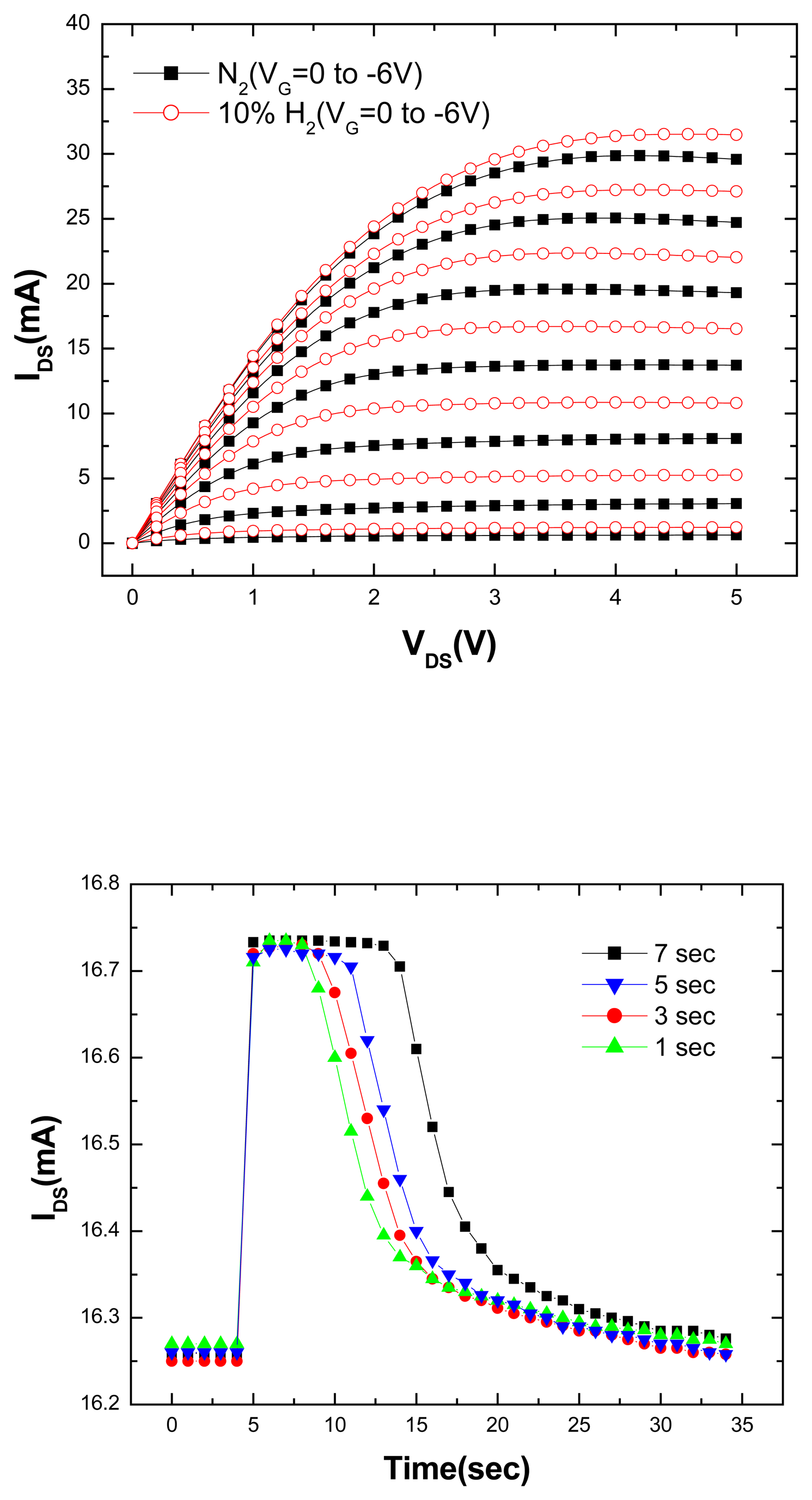
Figure 5 (top) shows the MOS-HEMT drain-source current voltage (I
DS-V
DS) characteristics at 25°C measured in both the pure N
2 and 10%H
2/90% N
2 ambients. The current is measurably larger in the latter case as would be expected if the hydrogen catalytically dissociates on the Pt contact and diffuses through the Sc
2O
3 to the interface where it screens some of the piezo-induced channel charge [
11,
12]. This is a clear demonstration of the sensitivity of AlGaN/GaN HEMT dc characteristics to the presence of hydrogen in the ambient in which they are being measured. The use of less efficient catalytic metals as the gate metallization would reduce this sensitivity, but operation at elevated temperatures would increase the effect of the hydrogen because of more efficient dissociation on the metal contact.
Figure 5 (bottom) shows some of the recovery characteristics of the MOS-HEMTs upon cycling the ambient from N
2 to 10%H
2/ 90% N
2. While the change in drain-source current is almost instantaneous (< 1 sec), the recovery back to the N
2 ambient value is of the order of 20 secs. This is controlled by the mass transport characteristics of the gas out of the test chamber, as demonstrated by changing the total flow rate upon switching the gas into the chamber. Given that the current change upon introduction of the hydrogen is rapid, the effective diffusivity of the atomic hydrogen through the Sc
2O
3 must be greater than 4 ×10
-12 cm
2/V.s at 25
oC. Note the complete reversibility of the drain-source current for repeated cycling of the ambient.
Sc
2O
3/AlGaN/GaN MOS-HEMTs show a marked sensitivity of their drain-source current to the presence of hydrogen in the measurement ambient [
10,
12]. This effect is due to the dissociation of the molecular hydrogen on the Pt gate contact, followed by diffusion of the atomic species to the oxide/semiconductor interface where it changes the piezo-induced channel charge. The MOS-HEMTs show larger changes in current than their corresponding MOS-diode or Schottky diode counterparts and show promise as sensitive hydrogen detectors.
Of particular interest are methods for detecting ethylene (C
2H
4), which offers problems because of its strong double bonds and hence the difficulty in dissociating it at modest temperatures. The forward diode current-voltage (I-V) characteristics at 400 °C of the Pt/Sc
2O
3/AlGaN/GaN MOS-HEMT diode both in pure N
2 and in a 10% C
2H
4/90%N
2 atmosphere show that at a given forward bias, the current increases upon introduction of the C
2H
4.In analogy with the detection of hydrogen in comparable SiC and Si Schottky diodes, a possible mechanism for the current increases involves atomic hydrogen either decomposed from C
2H
4 in the gas phase or chemisorbed on the Pt Schottky contacts then catalytically decomposed to release atomic hydrogen. The hydrogen can then diffuse rapidly though the Pt metallization and the underlying oxide to the interface where it forms a dipole layer and lowers the effective barrier height. We emphasize that other mechanisms could be present, however the activation energy for the current recovery is ∼1 eV, similar to the value for atomic hydrogen diffusion in GaN, which suggests that this is at least a plausible mechanism [
13].
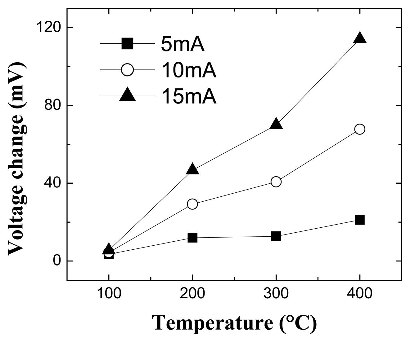
Figure 6 shows the change in voltage at fixed current as a function of temperature for the MOS diodes when switching from a 100 % N
2 ambient to 10% C
2H
4/90% N
2. As the detection temperature is increased, the response of the MOS-HEMT diodes increases due to more efficient cracking of the hydrogen on the metal contact. Note that the changes in both current and voltage are quite large and readily detected. In analogy with results for MOS gas sensors in other materials systems, the effect of the introduction of the atomic hydrogen into the oxide is to create a dipole layer at the oxide/semiconductor interface that will screen some of the piezo-induced charge in the HEMT channel [
13]. The time constant for response of the diodes was determined by the mass transport characteristics of the gas into the volume of the test chamber and was not limited by the response of the MOS diode itself.
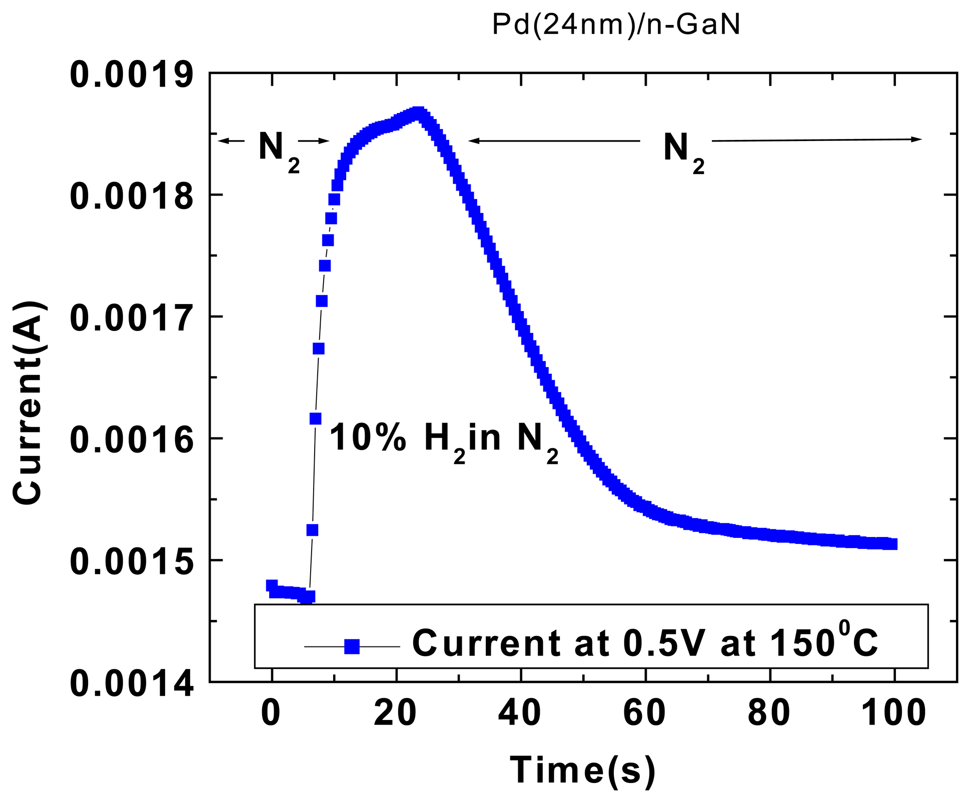
Simple Pt or Pd gate GaN Schottky diodes can also provide effective detection of combustion gases.
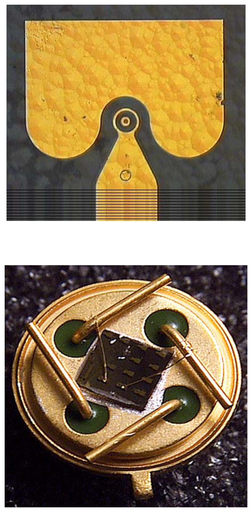
Figure 7 shows a plan view photograph of a two-terminal sensor, along with a device packaged into a header for testing. These devices produce easily measurable changes in forward current upon exposure to hydrogen-containing ambients, as shown in the I-V characteristics of
Figure 8. This data was taken at 150°C, but the changes are also measurable at room temperature, showing that the sensors do not need an on-chip heater to increase their detection efficiency, although of course they show larger current changes at higher temperatures.
2.3 Hydrogen-Selective Sensing at Room Temperature with ZnO Nanorods
The sensitivity for detecting hydrogen with multiple ZnO nanorods is found to be greatly enhanced by sputter-depositing clusters of Pd on the surface. The resulting structures show a change in room temperature resistance upon exposure to hydrogen concentrations in N2 of 10-500 ppm approximately a factor of five larger than without Pd. Pd-coated ZnO nanorods detected hydrogen down to < 10 ppm, with relative responses of >2.6 % at 10 ppm and > 4.2 % at 500 ppm H2 in N2 after 10 min exposure. There was no response at room temperature to O2. Approximately 95% of the initial ZnO conductance after exposure to hydrogen was recovered within 20s by exposing the nanorods to either air or pure O2.-This rapid and easy recoverability make the Pd-coated nanorods suitable for practical applications in hydrogen-selective sensing at ppm levels at room temperature with < 0.4 mW power consumption.
The site-selective growth of ZnO nanorods was achieved by nucleating the nanorods on a substrate coated with Au islands.-For nominal Au thicknesses of 20Å, discontinuous Au islands are realized.-ZnO nanorods were deposited by Molecular Beam Epitaxy (MBE) with a base pressure of 5 × 10
-8 mbar using high purity (99.9999%) Zn metal and an O
3/O
2 plasma discharge as the source chemicals. The Zn pressure was varied between 4 × 10
-6 and 2 × 10
-7 mbar, while the beam pressure of the O
3/O
2 mixture was varied between 5 × 10
-6 and 5 × 10
-4 mbar. The growth time was ∼2 h at 600°C.-The typical length of the resultant nanorods was 2∼10 μm, with typical diameters in the range of 30 – 150 nm.
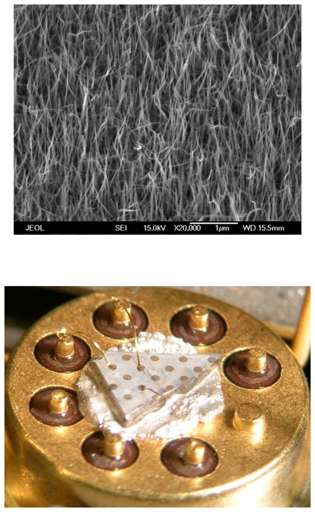
Figure 9 (top) shows a scanning electron micrograph of the as-grown rods. Selected area diffraction patterns showed the nanorods to be single-crystal.-In some cases, the nanorods were coated with Pd thin films (∼100Å thick) deposited by sputtering. This forms clusters of Pd with ∼70% coverage of the nanorod surface and root-mean-square roughness of ∼ 80Å.
A shadow mask was used to pattern sputtered Al/Ti/Au electrodes contacting both ends of multiple nanorods on the Al
2O
3 substrates. The separation of the electrodes was ∼30 um.-A picture of the packaged sensor is shown in
Figure 9 (bottom).-Au wires were bonded to the contact pad for current –voltage (I-V) measurements performed at 25°C in a range of different ambients (
,N
2, O
2 or 10-500 ppm H
2 in N
2). Note that no currents were measured through the discontinuous Au islands and no thin film of ZnO was observed with the growth condition for the nanorods. The I-V characteristics from the multiple nanorods were linear with typical currents of 0.8 mA at an applied bias of 0.5V.
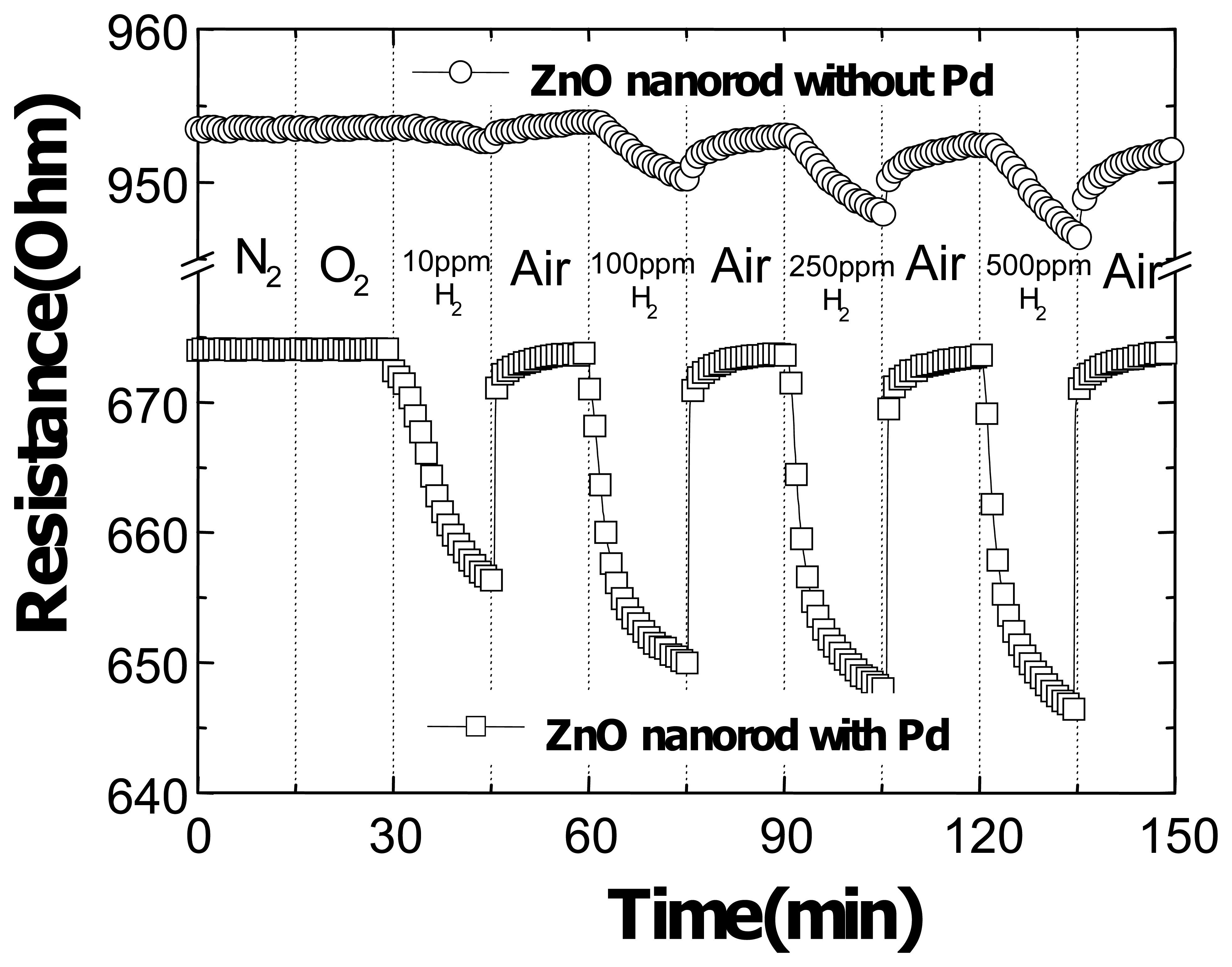
Figure 10 shows the time dependence of resistance of either Pt-coated or uncoated multiple ZnO nanorods as the gas ambient is switched from N
2 to various concentrations of H
2 in air (10-500 ppm) as time proceeds. There are several aspects of the data. First, there is a strong increase (approximately a factor of 5) in the response of the Pd-coated nanorods to hydrogen relative to the uncoated devices. The addition of the Pd appears to be effective in catalytic dissociation of the H
2 to atomic hydrogen. Second, there was no response of either type of nanorod to the presence of O
2 in the ambient at room temperature. Third, the effective conductivity of the Pd-coated nanorods is higher due to the presence of the metal. Fourth, the recovery of the initial resistance is rapid (<20 sec) upon removal of the hydrogen from the ambient, while the nanorod resistance is still changing at least 15 mins after the introduction of the hydrogen. The reversible chemisorption of reactive gases at the surface of metal oxides such as ZnO can produce a large and reversible variation in the conductance of the material. Fifth, the relative response of Pt-coated nanorods is a function of H
2 concentration in N
2. The Pd-coated nanrods detected hydrogen down to < 10 ppm, with relative responses of >2.6 % at 10 ppm and > 4.2 % at 500 ppm H
2 in N
2 after 10 min exposure, as shown in
Figure 11. By comparison, the uncoated devices showed relative resistance changes of ∼0.25% for 500 ppm H
2 in N
2 after 10 min exposure and the results were not consistent for lower concentrations. The gas sensing mechanisms suggested in the past include the desorption of adsorbed surface hydrogen and grain boundaries in poly-ZnO, exchange of charges between adsorbed gas species and the ZnO surface leading to changes in depletion depth and changes in surface or grain boundary conduction by gas adsorption/desorption. The detection mechanism is still not firmly established in these devices and needs further study. It should be remembered that hydrogen introduces a shallow donor state in ZnO and this change in near-surface conductivity may also play a role.
Figure 12 shows the time dependence of resistance change of Pt-coated multiple ZnO nanorods as the gas ambient is switched from vacuum to N
2, oxygen or various concentrations of H
2 in air(10-500 ppm) and then back to Air. This data confirms the absence of sensitivity to O
2. The resistance change during the exposure to hydrogen was slower in the beginning and the rate resistance change reached maximum at 1.5 min of the exposure time. This could be due to some of the Pd becoming covered with native oxide which is removed by exposure to hydrogen. Since the available surface Pd for catalytic chemical absorption of hydrogen increased after the removal of oxide, the rate of resistance change increased. However, the Pd surface gradually saturated with the hydrogen and the rate of resistance change decreased. When the gas ambient switched from hydrogen to air, the oxygen reacted with hydrogen right away, with the resistance of the nanorods changed back to the original value instantly. Moreover, the data was recorded at a power level of < 0.4 mW, which is low even in comparison with CNTs. This is attractive for long-term hydrogen sensing applications [
7,
9].
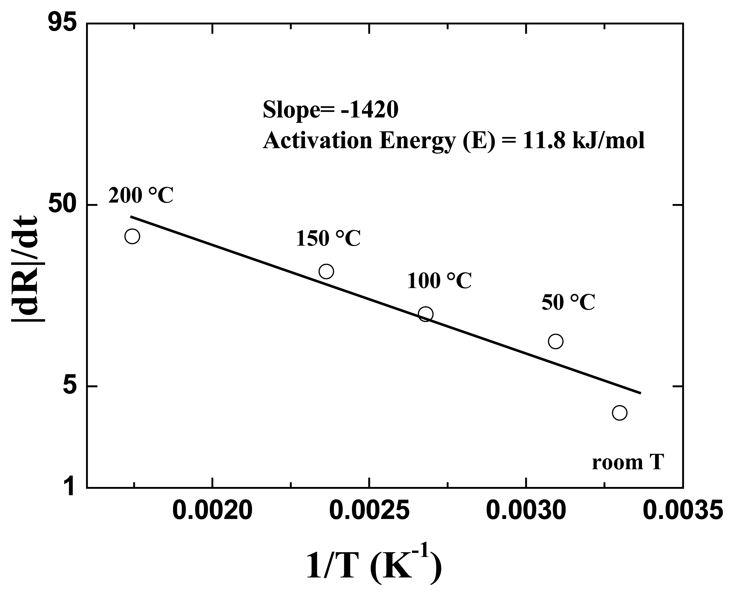
Figure 13 shows the Arrhenius plot of nanorod resistance change rate. The rate of resistance change for the nanorods exposed to the 500 ppm H
2 in N
2 was measured at different temperatures. An activation energy of 12KJ/mole was calculated from the slope of the Arrhenius plot. This value is larger than that of a typical diffusion process [
10,
14]. Therefore the dominant mechanism for this sensing process is more likely to be the chemisorption of hydrogen on the Pd surface.
In conclusion, Pd-coated ZnO nanorods appear well-suited to detection of ppm concentrations of hydrogen at room temperature. The recovery characteristics are fast upon removal of hydrogen from the ambient .The ZnO nanorods can be placed on cheap transparent substrates such as glass, making them attractive for low-cost sensing applications and operate at very low power conditions.
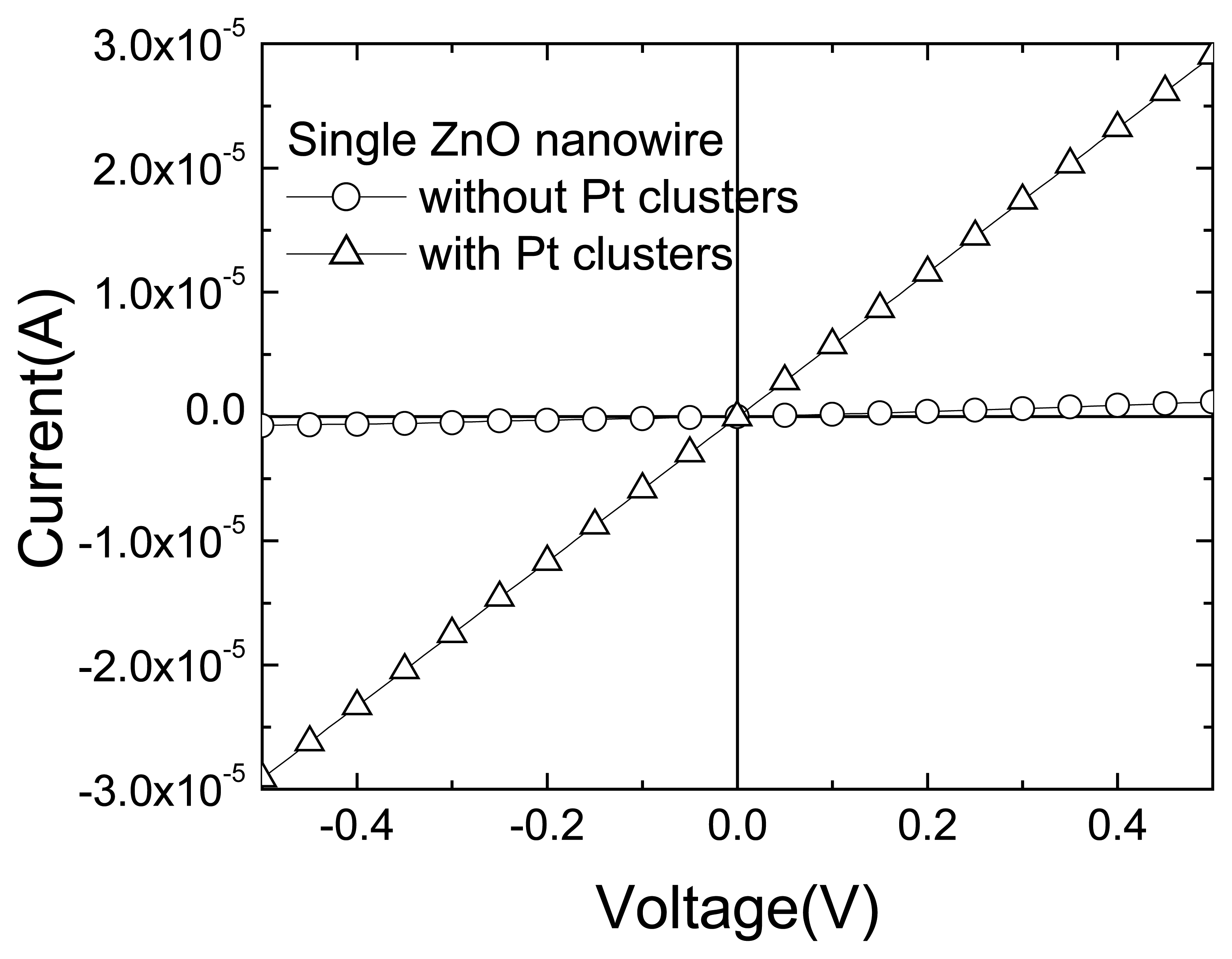
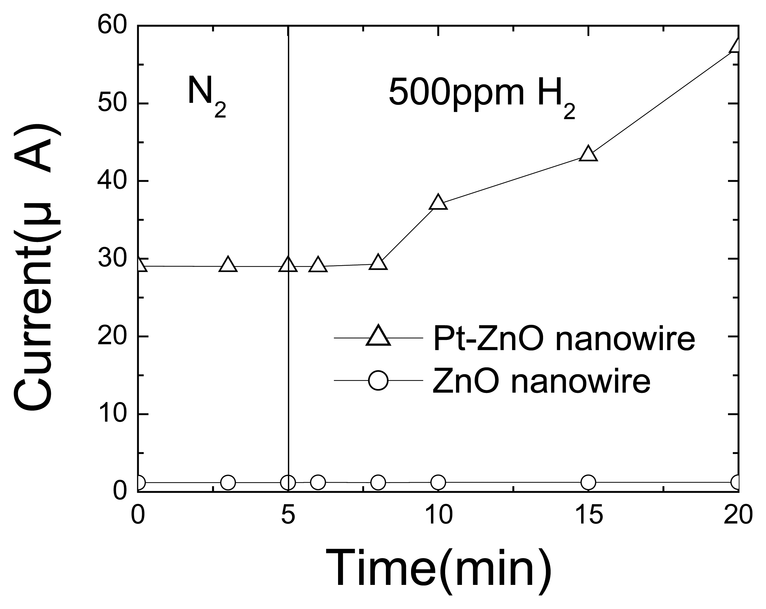
2.4 Room Temperature Hydrogen-Selective Sensing Using Single ZnO Nanorods at MicroWatt Power Levels
Single ZnO nanorods coated with Pt clusters by sputtering are shown to selectively detect hydrogen at room temperature. There were no differences in the current-voltage characteristics for measurement in air, N2 or vacuum. The single nanorods operate at extremely low power levels of ∼15-30 μW, which is approximately a factor of 25 lower than multiple ZnO nanorods operated under the same conditions. The addition of the Pt coatings increased the detection sensitivity of the nanorods for 500 ppm H2 in N2 by approximately an order of magnitude, which is about a factor of 2 improvement over the similar case for multiple nanorods. Pt-coated single ZnO nanorods showed relative responses of ∼20 % and 50%, respectively, after 10 mins or 20 mins exposure, respectively, to 500 ppm H2 in N2.
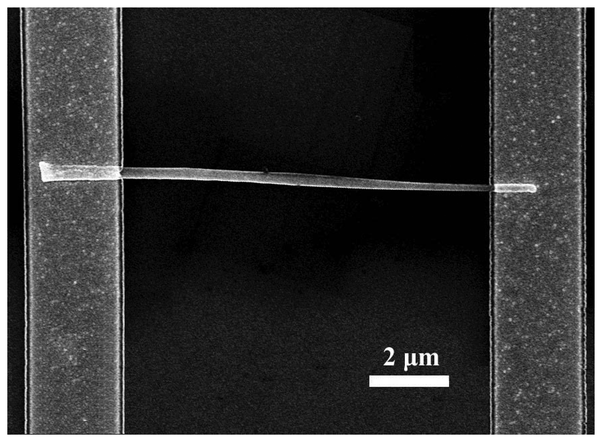
The site-selective growth of ZnO nanorods was achieved by nucleating the nanorods on a sapphire substrate coated with Au islands. A shadow mask was used to pattern sputtered Al/Ti/Au electrodes contacting both ends of single nanorods on the Si substrates. The separation of the electrodes was ∼10 um. In some cases, the nanorods were coated with discontinuous Pt cluster (∼10-20Å thick) deposited by sputtering. A scanning electron micrograph of the single nanorod sensor is shown in
Figure 14. Au wires were bonded to the contact pad for current–voltage (I-V) measurements performed at 25°C in a range of different ambients ( vacuum,N
2, O
2 or 100-500 ppm H
2 in N
2).
The I-V characteristics from the uncoated single nanorods were linear with typical currents in the μA at an applied bias of 0.5V.
Figure 15 shows that the addition of the Pt-coatings increased the effective conductivity of the nanorods by over an order of magnitude. Since the Pt films are discontinuous (as evidenced by both field-emission scanning electron microscopy and atomic force microscopy), this suggests that the sputtering process itself changes the resistance of the nanorods, most likely through the introduction of oxygen vacancies which are donor states in ZnO. There was a strong increase (approximately a factor of 5) in the response of the Pt-coated nanorods to hydrogen relative to the uncoated devices.
Figure 16 shows the I-V characteristics of Pt-coated nanorods as a function of both the measurement ambient and the time after exposure to 500 ppm H
2 in N
2. There are several aspects of the data. There was no response of either coated or uncoated nanorods to the presence of O
2 in the ambient at room temperature and indeed the I-V characteristics were independent of the measurement ambient for vacuum, air or pure N
2. By sharp contrast, the nanorods were sensitive to the presence of H
2 in the ambient, with the response being time-dependent. The nanorod resistance was still changing at least 15 mins after the introduction of the hydrogen. An Arrhenius plot of the rate of resistance change for the nanorods exposed to the 500 ppm H
2 in N
2 for 10 mins produced an activation energy of ∼15KJ/mole. This is larger than that expected for typical diffusion processes and suggests that the rate-limiting step maybe chemisorption of hydrogen on the Pt surface [
11,
13]. The reversible chemisorption of reactive gases at the surface of ZnO can produce a large reversible variation in the resistance. In addition, atomic hydrogen introduces a shallow donor state into ZnO and this may play a role in the increased conductance of the nanorods. The diffusion coefficient of the hydrogen is also much faster in ZnO than in any other wide bandgap semiconductor. Note the very low power consumption of the nanorod sensors, which is in the range 15-30 μW. This is approximately a factor of 25 lower than multiple ZnO nanorods operated under the same conditions and more than a factor of 50 lower than carbon nanotubes doped with Pd that were used for hydrogen detection. The low power consumptions is clearly of advantage in many types of remote sensing or long-term sensing applications.
Figure 17 shows the time dependence of current (top) in both the uncoated and Pt-coated nanorods exposed to 500 ppm H
2 in N
2. The relative resistance responses were ∼20 % and 50%, respectively, after 10 mins or 20 mins exposure. By comparison, the uncoated devices showed relative resistance changes of ∼ 2% and 3%, respectively, after 10 min or 20 min exposure. The resistance change during the exposure to hydrogen was slower in the first few minutes, as is clear in
Figure 17. This may be due to removal by the atomic hydrogen of native oxide on the Pt. As the effective surface area of the Pt would increase as the oxide was removed, the rate of change of resistance due to hydrogen adsorption should also increase.
In summary, Pt-coated ZnO single nanorods are shown to selectively detect hydrogen at room temperature with very low power consumption. The disadvantage of this approach relative to using a network of multiple nanorods is the additional processing that is needed to contact a single nanorod, but the power consumption is significantly(a factor of ∼25) lower.
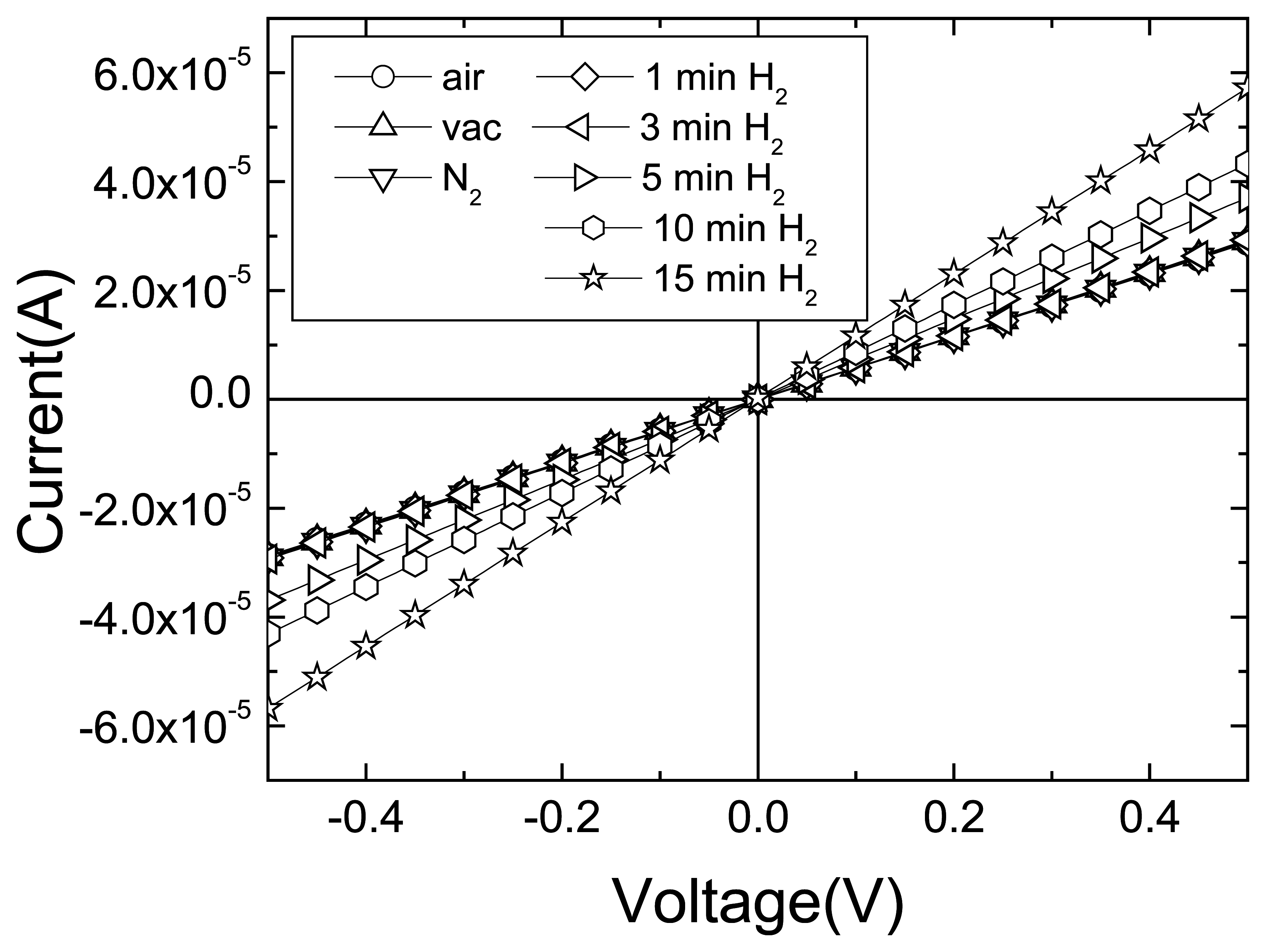
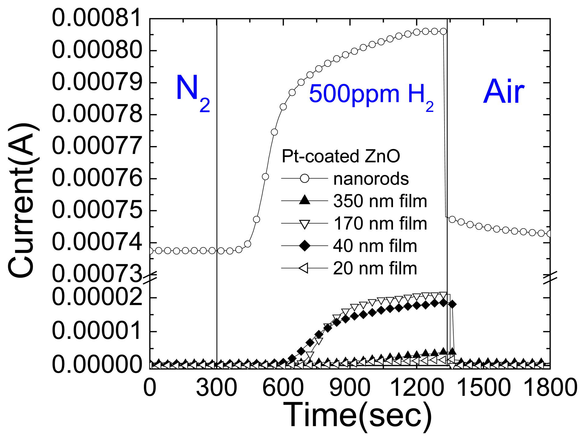
2.5 Hydrogen Sensing at Room Temperature with Pt-coated ZnO Thin Films and Nanorods
A comparison is made of the sensitivities for detecting hydrogen with Pt-coated single ZnO nanorods and thin films of various thicknesses (20-350 nm). The Pt-coated single nanorods show a current response approximately a factor of three larger at room temperature upon exposure to 500ppm H2 in N2 than the thin films of ZnO. The power consumption with both types of sensors can be very small (in the nW range) when using discontinuous coatings of Pt. Once the Pt coating becomes continuous, the current required to operate the sensors increases to the μW range. The optimum ZnO thin film thickness under our conditions was between 40-170 nm, with the hydrogen sensitivity falling off outside this range. The nanorod sensors show a slower recovery in air after hydrogen exposure than the thin films, but exhibit a faster response to hydrogen, consistent with the notion that the former adsorb relatively more hydrogen on their surface. Both ZnO thin and nanorods cannot detect oxygen.
There is strong current interest in the development of lightweight hydrogen sensors capable of ppm sensitivity and extended operation at low power levels [
4-
6,
11,
13]. The applications for these sensors include combustion gas detection in spacecraft and solid oxide fuel cells with proton-exchange membranes (PEM). Structures such as nanorods and nanotubes are natural candidates for these applications. To enhance the detection sensitivity for hydrogen, the use of catalytic Pt or Pd coatings or doping on semiconductors (either films or nanorods) and carbon nanotubes can increase the dissociation efficiency of molecular hydrogen to the more reactive atomic form. ZnO is attractive for sensing applications because of its wide bandgap (3.2 eV), the availability of heterostructures, the ease of synthesizing nanostructures and the bio-safe characteristics of this material. A number of previous reports have shown that ZnO with Pd nanoparticles can increase the detection sensitivity for H
2. The high surface-volume ratio of nanorods makes them attractive for detecting hydrogen at low concentrations and it is relatively straightforward to synthesize ZnO nanostructures on a wide variety of substrates. However, to this point, there has been no clear demonstration of improved detection sensitivity with nanorods compared to thin films.
Two types of ZnO were employed in these experiments. The thin films were grown by Pulsed Laser Deposition on sapphire substrates at 450°C. The ZnO thickness was varied from 20-350 nm. The films were nominally undoped with low n-type (1017 cm-3) carrier concentration. Top-side Ohmic contacts of sputtered Al/Ti/Au were patterned by lift-off. The site-selective growth of ZnO nanorods was achieved by nucleating the nanorods on a substrate coated with Au islands as has also been described in detail previously. For nominal Au thicknesses of 20Å, discontinuous Au islands are realized. ZnO nanorods were deposited by Molecular Beam Epitaxy (MBE) with a base pressure of 5×10⁻⁸ mbar using high purity (99.9999%) Zn metal and an O3/O2 plasma discharge as the source chemicals. The Zn pressure was varied between 4×10⁻⁶ and 2×10⁻⁷ mbar, while the beam pressure of the O3/O2 mixture was varied between 5 × 10⁻⁶ and 5×10⁻⁴ mbar. The growth time was ∼2 h at 600°C. The typical length of the resultant nanorods was 5∼15 μm, with typical diameters in the range of 50∼150 nm. Selected area diffraction patterns showed the nanorods to be single crystal. For the multiple nanorods, a shadow mask was used to pattern sputtered Al/Ti/Au electrodes on the ZnO nanorods/Al2O3 substrates. The separation of the electrodes was ∼400μm. In some cases, the sensors were coated with Pt thin films (∼10Å thick) deposited by sputtering. Au wires were bonded to the contact pad for current–voltage (I-V) measurements performed at 25°C in air, N2 or 500 ppm H2 in N2. No currents were measured through the discontinuous Au islands.
The I-V characteristics measured between the Ohmic contacts on the thin film ZnO samples of either 20 or 350 nm thickness, both before and after the Pt deposition on the surface show an increase in current upon exposure to hydrogen. The current increase as a result of the Pt deposition is approximately a factor of two for the thinnest sample and remains in the nA range at 0.5V bias, ie. the power consumption is 4nW at this operating voltage. The effective conductivity of the Pt-coated films is higher due to the presence of the metal. At longer Pt sputtering times we would typically see a transition to much higher currents as the Pt film became continuous and the conductivity of the structure was no longer determined by the ZnO layer itself.
Figure 18 (top) shows the time dependence of current change at 0.5 V bias on the Pt-coated ZnO films of different thickness as the gas ambient is switched from N
2 to 500ppm H
2 in N
2 and back to air as time proceeds. This data shows that the sensors are insensitive to N
2 and that there is a strong ZnO thickness dependence to the response to hydrogen. The bottom of
Figure 18 shows the change in current at 0.5 V bias when switching from N
2 to the hydrogen-containing ambient for the ZnO films of different thickness. At small thicknesses, the current change is small, which is probably related to poorer crystal quality and also at large film thickness where the bulk conductivity dominates the total resistance.
Figure 19 shows the time dependence of current in both the Pt-coated multiple ZnO nanorods and the thin films as the gas ambient is switched from N
2 to 500 ppm H
2 in N
2 and then back to air as time proceeds. It is clear that the nanorods have a much larger response (roughly a factor of 3 even for the optimal response for the thin films) to the introduction of hydrogen into the ambient compared to their thin film counterparts. This is consistent with the expectation of a higher relative response based on their larger surface-to-volume ratio.
Although not shown here, there was no response of either type of sensors to the presence of O
2 in the ambient at room temperature. The recovery of the initial resistance is rapid (90%, <20 sec) upon removal of the hydrogen from the ambient by either O
2 or air, while the nanorod resistance is still changing at least 15 mins after the introduction of the hydrogen. The response is faster at higher temperatures. The nanorods show a slower recovery than the thin films, most likely due to the relatively higher degree of hydrogen adsorption. The expected sensing mechanism suggested previously is that reversible chemisorption of the hydrogen on the ZnO produces a reversible variation in the conductance, with the exchange of charges between the hydrogen and the ZnO surface leading to changes in depletion depth [
11,
13]. The conductivity of both ZnO thin film and nanorods did change when the ambient switched from N
2 to Air.
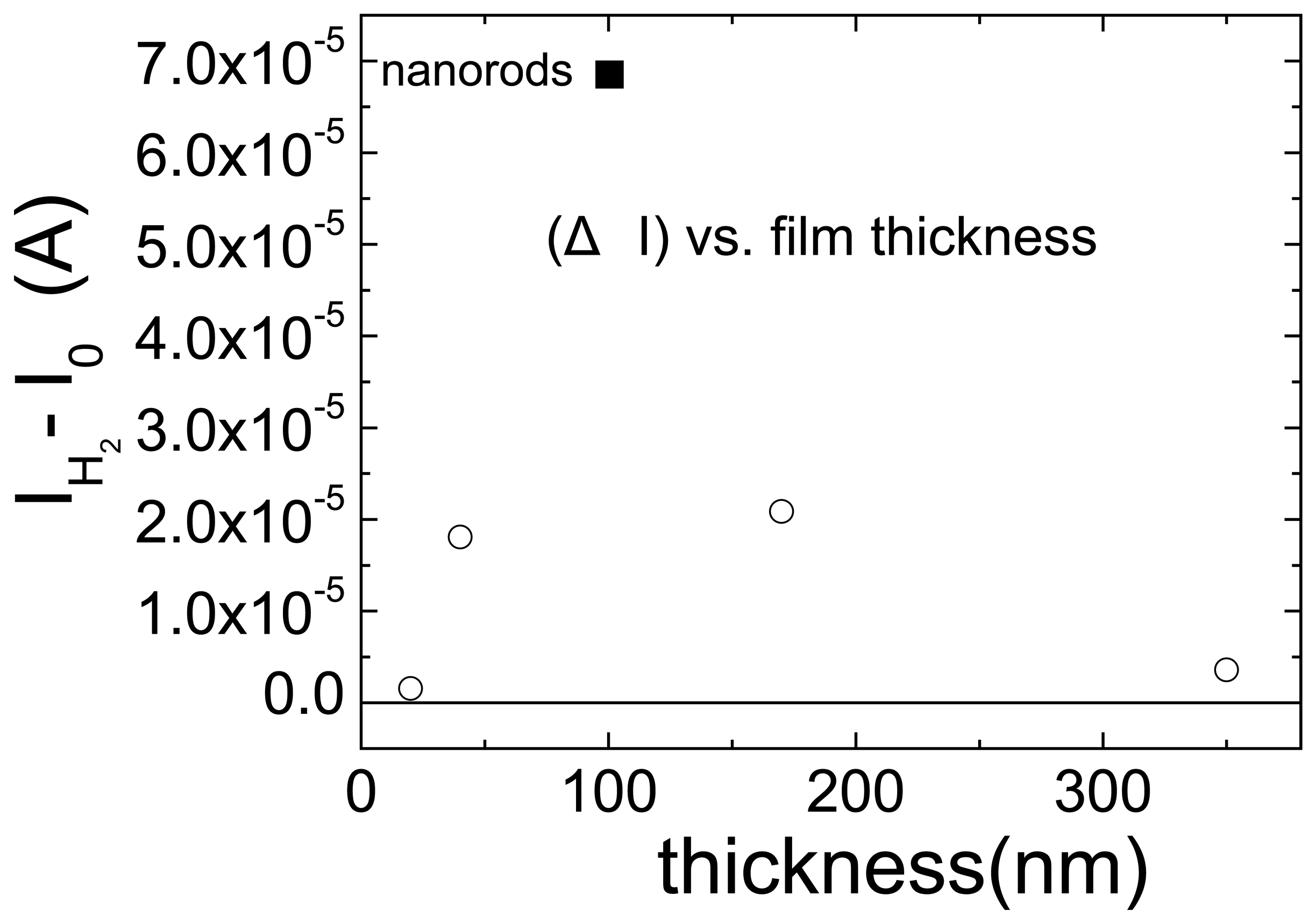
Figure 20 shows the maximum current change at 0.5 V bias for exposure of the nanorods and thin films to the 500 ppm H
2 in N
2.
As discussed earlier, a key requirement in long-term hydrogen sensing applications is the sensor power consumption [
7-
10]. Both the thin film and multiple nanorod sensors can operate at ≤ 0.5V bias and powers ≤ 4 nW. We have also demonstrated hydrogen sensing with single ZnO nanorods at power levels approximately an order of magnitude lower than this, but the devices show poorer long-term current stability than multiple nanorod sensors.
In conclusion, Pt-coated ZnO thin films and multiple nanorods both are capable of detection of ppm concentrations of hydrogen at room temperature. The thin films show optimum responses to the presence of hydrogen at moderate thicknesses. The nanorods show larger responses to hydrogen than the thin films, consistent with their large surface-to-volume ratios and have the advantage in terms of flexibility of the choice of substrate.
