
Smart pH Sensing: A Self-Sensitivity Programmable Platform with Multi-Functional Charge-Trap-Flash ISFET Technology

Department of Electronic Materials Engineering, Kwangwoon University, Gwangun-ro 20, Nowon-gu, Seoul 01897, Republic of Korea
*
Author to whom correspondence should be addressed.
Sensors 2024, 24(3), 1017; https://doi.org/10.3390/s24031017
Submission received: 8 January 2024
/
Revised: 1 February 2024
/
Accepted: 2 February 2024
/
Published: 4 February 2024
(This article belongs to the Special Issue Biosensors and Electrochemical Sensors)
Abstract
:This study presents a novel pH sensor platform utilizing charge-trap-flash-type metal oxide semiconductor field-effect transistors (CTF-type MOSFETs) for enhanced sensitivity and self-amplification. Traditional ion-sensitive field-effect transistors (ISFETs) face challenges in commercialization due to low sensitivity at room temperature, known as the Nernst limit. To overcome this limitation, we explore resistive coupling effects and CTF-type MOSFETs, allowing for flexible adjustment of the amplification ratio. The platform adopts a unique approach, employing CTF-type MOSFETs as both transducers and resistors, ensuring efficient sensitivity control. An extended-gate (EG) structure is implemented to enhance cost-effectiveness and increase the overall lifespan of the sensor platform by preventing direct contact between analytes and the transducer. The proposed pH sensor platform demonstrates effective sensitivity control at various amplification ratios. Stability and reliability are validated by investigating non-ideal effects, including hysteresis and drift. The CTF-type MOSFETs’ electrical characteristics, energy band diagrams, and programmable resistance modulation are thoroughly characterized. The results showcase remarkable stability, even under prolonged and repetitive operations, indicating the platform’s potential for accurate pH detection in diverse environments. This study contributes a robust and stable alternative for detecting micro-potential analytes, with promising applications in health management and point-of-care settings.
1. Introduction
In recent years, amid global health concerns and increased life expectancies, health management and point-of-care (PoC) applications have garnered significant attention [1,2,3,4]. Reflecting this trend, a fundamental biosensor, the pH sensor, has gained particular attention. Among pH sensors, the ion-sensitive field-effect transistor (ISFET) based on the metal oxide semiconductor field-effect-transistor (MOSFET) structure has been particularly extensively researched. While other pH sensors, such as optical fiber pH sensors, fluorometric pH sensors, and biosensor-based pH sensors, are also under investigation, they have not become primary research topics due to drawbacks such as complexity, high cost, labeling, and the instability of measurement results [5,6,7,8,9,10]. ISFETs stand out with advantages such as accurate sensing operation, label-free detection, compact size, rapid response, and compatibility with complementary metal oxide semiconductor (CMOS) processes, distinguishing itself from these alternatives [11,12,13,14].
However, the commercialization of ISFETs is hindered by its low sensitivity at room temperature (59.14 mV/pH), which is known as the Nernst limit [15,16,17]. Due to the fundamental role of pH sensors, used as diagnostic devices for diseases and environmental pollution, it is crucial to ensure their accurate sensing capabilities for even trace amounts. The Nernst limit is the most significant limitation that hinders precise and high-sensitive detection, which is essential for early problem detection. Addressing this limitation using external amplification circuits results in increased power consumption and complicates the sensor platforms. As an alternative, studies have explored the direct implementation of amplification capabilities in ISFET devices. Notable methods for self-amplification include capacitive and resistive coupling effects [18,19,20,21,22,23].
Capacitive coupling effects leverage the electrical amplification effect between the top- and bottom-gate insulators in a dual-gate (DG) structure. However, this approach poses challenges because the amplification ratio is determined by the dielectric capacitance ratio and cannot be adjusted after fabrication. By contrast, resistive coupling effects utilize the resistance ratio between two resistors to determine the amplification ratio, which facilitates the development of adjustable ratios via the modulation of the resistance of the resistors. The adjustability of the amplification ratio implies that the sensor characteristics can be modified according to the user’s preferences such as power consumption, sensitivity, and stability. This essentially means that a single sensor can effectively adapt to complex scenarios, meeting the user’s desired parameters. A crucial consideration in adjusting the amplification ratio is the selection of devices for the resistors. Adopting charge-trap-flash (CTF) memory devices facilitates the effective implementation of a wide range of amplification ratios through the modulation of the channel resistance changes according to the program or erasure modes [24,25,26].
This study developed a sensor platform using resistive coupling effects and CTF-type MOSFETs, enabling the flexible adjustment of the amplification ratio. An efficient multifunctional system was implemented by employing multiple CTF-type MOSFET devices, each with the same structure as the transducer and resistor. This was realized owing to the unique characteristics of the CTF-type MOSFET used as a transducer, which employed channel resistance modulation owing to charge trapping, similar to a variable resistor [24,25]. Conventional ISFET structures suffer from a vulnerability wherein analytes (pH buffer solution) directly contact the transducer, rendering the entire platform susceptible to contamination and reducing its lifespan. To overcome this, this study adopted an extended-gate (EG) structure to enhance the cost-effectiveness and increase the overall lifespan of the sensor platform [27,28,29]. The pH sensitivity of the proposed sensor platform was evaluated at various amplification ratios to confirm its effective sensitivity control. Furthermore, to validate the stability and reliability of the proposed sensor platform, we investigated non-ideal effects, such as hysteresis and drift effects [30,31,32,33,34].
2. Materials and Methods
2.1. Fabrication of the Multi-Functional Charge-Trap-Flash-Type Field-Effect Transistor
The proposed pH sensor platform relied on a multifunctional CTF-type MOSFET that served as both a transducer and a resistor. The CTF-type MOSFET with a DG structure prepared in this study used p-type (100) bonds and etch-back silicon-on-insulator (BESOI) wafers. The thicknesses of the top-silicon and buried-oxide (BOX) layers was 100 nm and 750 nm, respectively. The top-silicon layer, a MOSFET channel, was a p-type single-crystal silicon with 1 × 1015 cm−3 of boron doping. The active region of the top-Si layer was defined using photolithography and reactive-ion etching (RIE) with SF6 gas. Subsequently, a 100 nm thick heavily phosphorus (n+)-doped poly-Si layer was deposited for source/drain (S/D) using low-pressure chemical vapor deposition (LPCVD) at 650 °C. Post-deposition-annealing (PDA) was performed via rapid thermal annealing (RTA) at 850 °C (30 s, N2). The n+-doped poly-Si layer, except for the S/D region, was completely removed using RIE, and the top-Si layer was etched to a thickness of 40 nm for the channel. As a result, a DG-type nMOSFET with n+-doped poly-Si S/D and a thin channel with a 40 nm thickness was fabricated. Surface damage and roughness resulting from the thinning process were carefully eliminated using an ammonia peroxide solution. Channels were defined with widths and lengths of 10 μm each. Before forming the crucial components, a charge-trap layer (CTL), a barrier layer (BL), and a tunneling barrier were established. The tunneling barrier comprised an ONO structure stacked as a 2 nm thick SiO2 film (thermal oxidation), a 2 nm thick Si3N4 film (LPCVD), and a 3 nm thick SiO2 film (LPCVD). Subsequently, a 5 nm thick HfO2 film for the CTL and a 12 nm thick Al2O3 film for the BL were deposited using atomic layer deposition (ALD). To enhance the electrical properties of the thin films, PDA was conducted using RTA at 850 °C (30 s, N2). Electrodes were formed using a 20/100 nm thick Ni/Al thin film deposited using an electron-beam evaporator. Forming-gas annealing (FGA) at 450 °C (30 min, 2% H2/N2 mixture) removed any dangling bonds and internal defects in the thin film. Figure 1a shows an optical microscopy image of the fabricated CTF-type MOSFET, and Figure 1b illustrates the schematic structure and cross-sectional view of the thin-film layers.
2.2. Characterizations of the Self-Sensitivity Programmable pH Sensor Platform
We assessed the electrical characteristics of the self-sensitive programmable pH sensor platform using an Agilent 4156 B precision semiconductor parameter analyzer (Santa Clara, CA, USA). The device was positioned in a dark box to eliminate optical and electrical interference from the external environment. Pulse application for the channel resistance modulation of the CTF-type MOSFET was achieved using a waveform generator (RIGOL DG900, Suzhou, China). To analyze the pH response, a commercial ceramic plug junction-type Ag/AgCl electrode (Horiba 2080-06T, Kyoto, Japan) with an internal solution of AgCl-saturated KCl electrolyte served as the reference electrode. All measurements were recorded in a dark box in a controlled environment to ensure accuracy. To evaluate the hysteresis and drift effects, we conducted several tests to assess the reliability of the sensor platform under repeated and continuous operations. Hysteresis voltage (VH) was determined through calculations of the difference in reference voltage (VREF) between the initial and final pH states in the pH loop of [7→4→7→10→7]. Furthermore, the drift effect was observed by monitoring the shift in the VREF when exposing the SnO2 sensing membrane to a buffer solution of pH 7 for 10 h.
2.3. Signal Amplification of the Self-Sensitivity Programmable pH Sensor Platform
The self-sensitivity programmable pH sensor platform demonstrated variable amplification ratios during sensing operations, depending on the resistance ratios of the control gate resistor (RCG) and sensing gate resistor (RSG). The sensing gate (SG) comprised an EG, pH buffer solutions, and a reference electrode. This conveyed the surface potential changes owing to the adsorption and desorption of hydrogen ions to and from the transducer. The control gate (CG) was connected to an Agilent 4156B, which supplied the operational voltage to the transducer. In this configuration, RCG, RSG, and transducer utilized the same CTF-type MOSFET. Changes were employed in the channel resistance of the device as resistors through pulsed applications. However, the achievement of channel resistance modulation in the CTF-type MOSFET for signal amplification necessitated high voltage (over ∣7∣ V). Consequently, the sensing operation of the transducer, limited to the −5–5 V range, avoided inducing changes in the channel resistance, enabling the implementation of a multifunctional device. The equivalent circuit of the proposed self-sensitivity-programmable pH sensor platform is shown in Figure 2. The gate voltage (VG) of ISFETs is expressed as Equation (1). The voltage between CG and SG is expressed as Equation (2). A change in the potential of SG (Δψ0) was amplified by the resistive coupling ratio (RCG/RSG), causing a change in VCG. This implied that even micro-potential analytes could be detected with high sensitivity via resistive coupling [18,26].
3. Results and Discussion
3.1. Evaluation of the Multi-Functional Charge-Trap-Flash-Type Field-Effect Transistor
Figure 3a,b show the typical electrical characteristics of the transfer (ID–VG) and output (ID–VD) curves, respectively. As shown in Figure 3a, the drain current (ID) was recorded at a constant drain voltage (VD) of 1 V while applying a VG ranging from −3 to 5 V. The threshold voltage (VTH) was determined via linear extrapolation of the ID–VG curve in the linear region. Figure 3b illustrates ID as VG–VTH changed from 0 to 4 V across 11 steps. The current exhibited a linear increase in the low VD region and subsequently pinched off as VD increases, resulting in saturation characteristics.
The electrical parameters of the multi-functional CTF-type MOSFET were derived using the following equations [35,36]
and
where W is the channel width, L is the channel length, Cox is the capacitance per unit area of the gate oxide, and gm is the transconductance. The values extracted for various electrical parameters from the multi-functional CTF-type MOSFET were as follows: VTH was approximately −0.25 V, the on/off current ratio (Ion/Ioff) was 1.49 × 10⁷, the field-effect mobility (μFE) was 234.92 cm2/V·s, and the subthreshold swing (SS) was 234.92 mV/dec. Table 1 summarizes the electrical parameters.
Figure 4a,b show the energy band diagrams of the thin-film layer of the MAHONOS stack under non-, positive-, and negative-gate-bias conditions, respectively [37,38,39]. In these diagrams, the Al2O3 layer functioned as a BL, offering a high dielectric constant, significantly large bandgap offset, and substantial physical oxide thickness (POT) [40,41,42]. The selection of the HfO2 layer as the CTL was motivated by its higher trap density, greater dielectric constant, and lower bandgap offset compared with Al2O3 or SiO2 layers [43,44,45,46,47]. The engineered ONO structure, referred to as the variable oxide thickness (VARIOT) tunnel barrier, exhibited notable sensitivity to the electric field generated by the gate bias [48,49]. When the energy level of the electrons within the silicon channel was lower than that of the potential barrier, the ONO barrier functioned as an obstacle to electron penetration [50,51,52,53]. However, a substantial electric field induced significant band bending within the ONO barrier, allowing the electron wavefunction to tunnel through the thin triangular potential barrier. Consequently, the channel conductance in the CTL was modulated through charge trapping (leading to decreased conductance) or de-trapping (leading to increased conductance). In the retention mode, the trapped charges remained stable in the CTL, and the charge loss rate decreased owing to the substantial POT of the ONO barrier [54,55,56].
Figure 5 shows the transfer curves (a), hysteresis resistance (b), and retention time (c) corresponding to the program/erasure mode of the CTF-type MOSFET. We define the normal state of the CTF-type MOSFET as the state without an external voltage, the state after applying a positive bias as the program state, and the state after applying a negative bias as the erasure state. The changes in the electrical characteristics were measured for each state [57,58,59].
In the program mode, 50 pulses of 9.4 V with a duration of 100 ms were applied, whereas −10 V was utilized in the erasure mode. Depending on the magnitude and type of voltage applied to the gate, a VTH shift of approximately 1.47 V occurred. This shift was attributed to charge trapping and de-trapping, induced by the voltage applied to the top gate [60,61,62].
Hysteresis resistance was observed by cycling through a [normal–program–normal–erasure–normal] operation loop, and the change in the channel resistance after the loop was measured by expressing the difference between the initial and final values as ΔRnormal. The measured value of ΔRnormal was 645.48 Ω, representing approximately 5.33% of the resistance value in the normal state.
The retention time, which indicates how long the changed channel resistance is maintained for after the program/erasure mode, was also investigated [63,64,65]. Through the analysis of the records measured over 10,000 s, the change in resistance after 10 years was estimated. Percentage changes were observed as +22.28% at ×0.5, −2.02% at ×1, and −21.41% at ×5.
The measured results confirmed that the channel resistance modulation of the CTF-type MOSFET demonstrated significant stability, even under long-term and repetitive conditions. This indicates that there are no issues with its operation as a resistor in the proposed self-sensitivity programmable pH sensor platform.
Figure 6 depicts the channel resistance modulation of CTF-type MOSFET under various input voltage conditions. To construct a self-sensitive programmable pH sensor platform, it is crucial to accurately determine the RCG and RSG values for amplification. Therefore, this study investigated the channel resistance modulation according to the applied voltage type of the CTF-type MOSFET used as a resistor.
The objective of this experiment was to broadly configure the channel resistance variation based on the program/erase operation of the memory device, allowing the implementation of various amplification ratios. To secure various channel resistance modulation conditions, pulse-type program/erase voltages were applied instead of constant voltage. The pulse conditions used for measurements included pulse numbers of 1–50, pulse amplitudes of −10–10 V, and durations of 1–1000 ms. Resistance extraction was conducted for a total of 252 conditions, and the extracted resistance values ranged from 6.62 to 91.55 kΩ based on the measurement results. Therefore, it was confirmed that sensitivity adjustment is possible, ranging from a minimum of ×0.07 to a maximum of ×13.83 when combining resistance ratios. This signifies the successful fulfillment of the minimum conditions for constructing a self-sensitivity programmable pH sensor platform. Based on these results, subsequent measurements were implemented, with the amplification ratio specified as ×0.5, ×1, and ×5.
3.2. pH Sensing Characteristics of the Self-Sensitivity Programmable pH Sensor Platform
To evaluate the pH detection and signal amplification capabilities of the proposed pH sensor platform, we established the amplification ratio and examined the changes in the transfer curve as a function of CG. Figure 7 shows the alterations in the transfer curve when the amplification ratios were set to ×0.5, ×1, and ×5. The transfer curve was recorded in the range of −5–5 V using a buffer solution with pH values of 3, 4, 6, 7, 9, and 10. The sensing operation range was determined based on the conditions verified in Figure 6, setting it to the range (∣V∣ < 7 V) where the channel resistance of the transducer unit, the CTF-type MOSFET, remained unchanged.
The pH buffer solution that came into contact with the EG sensing unit caused a change in surface potential through ion adsorption on the sensing membrane’s surface. This change was then transmitted through the EG electrode to the top gate of the CTF-type MOSFET. In this process, ΔVSG was amplified in proportion to the ratio of RCG/RSG, leading to variations in the VTH shift of the transfer curves. As observed in Figure 7, surface potential changes due to pH sensing occur more prominently with increasing amplification ratios, resulting in a noticeable shift in the transfer curve. Consequently, the variation in VREF is determined accordingly.
Figure 8 shows the sensitivity data extracted from each transfer curve. The amplification ratio was determined via adjustments to the RCG/RSG value, resulting in pH sensitivities of ×0.49 amplification (28.02 mV/pH), ×1 amplification (56.96 mV/pH), and ×4.85 amplification (276.06 mV/pH). Also, the linearity of each sensitivity value was 98.51% at ×0.49 amplification, 98.88% at ×1 amplification, and 98.95% at ×4.85 amplification, respectively.
The measurement results demonstrate that the proposed self-sensitivity programmable pH sensor platform achieved sensitivities close to the configured amplification ratios while also ensuring excellent linearity for pH buffer solutions with different values. This indicates the successful and stable implementation of the intended sensitivity programming capability.
To assess the stability of the proposed pH sensor platform during repeated and continuous operation, we evaluated the non-ideal effects, including hysteresis and drift [66,67,68]. In Figure 9a, the hysteresis voltage is presented after a pH loop [7→10→7→4→7]. This was evaluated to estimate the stability in environments where different analytes needed to be detected repeatedly. The measurements were carried out at 2 min intervals for a total of 35 cycles in accordance with the specified pH loop, defining the hysteresis voltage as the difference between the initial and final values. The measured results showed values of 7.34, 9.98, and 13.05 mV for amplification ratios of ×0.5, ×1, and ×5, respectively. Figure 9b illustrates the drift effect measured after 10 h of exposure to a pH 7 buffer solution, evaluated in relation to stability when measuring a specific analyte over an extended period. The drift rate was expressed as a function of time, representing the difference between the initial and final values after 10 h of measurement. The measured results showed values of 3.71, 6.74, and 12.18 mV/h for amplification ratios of ×0.5, ×1, and ×5, respectively.
In both hysteresis voltage and drift rate, the measured results showed an increasing trend in non-ideal effect values with the rising amplification ratio. However, since the rate of increase in non-ideal effect values was considerably lower than the increase in sensitivity, it was evident that the benefits of increased sensitivity through amplification outweighed the negative impact of increased non-ideal effects through amplification. These results indicate that the proposed self-sensitivity programmable pH sensor platform demonstrates excellent stability. As the amplification ratio increases, the platform effectively withstands non-ideal effects, even in a continuous and repetitive measurement environment.
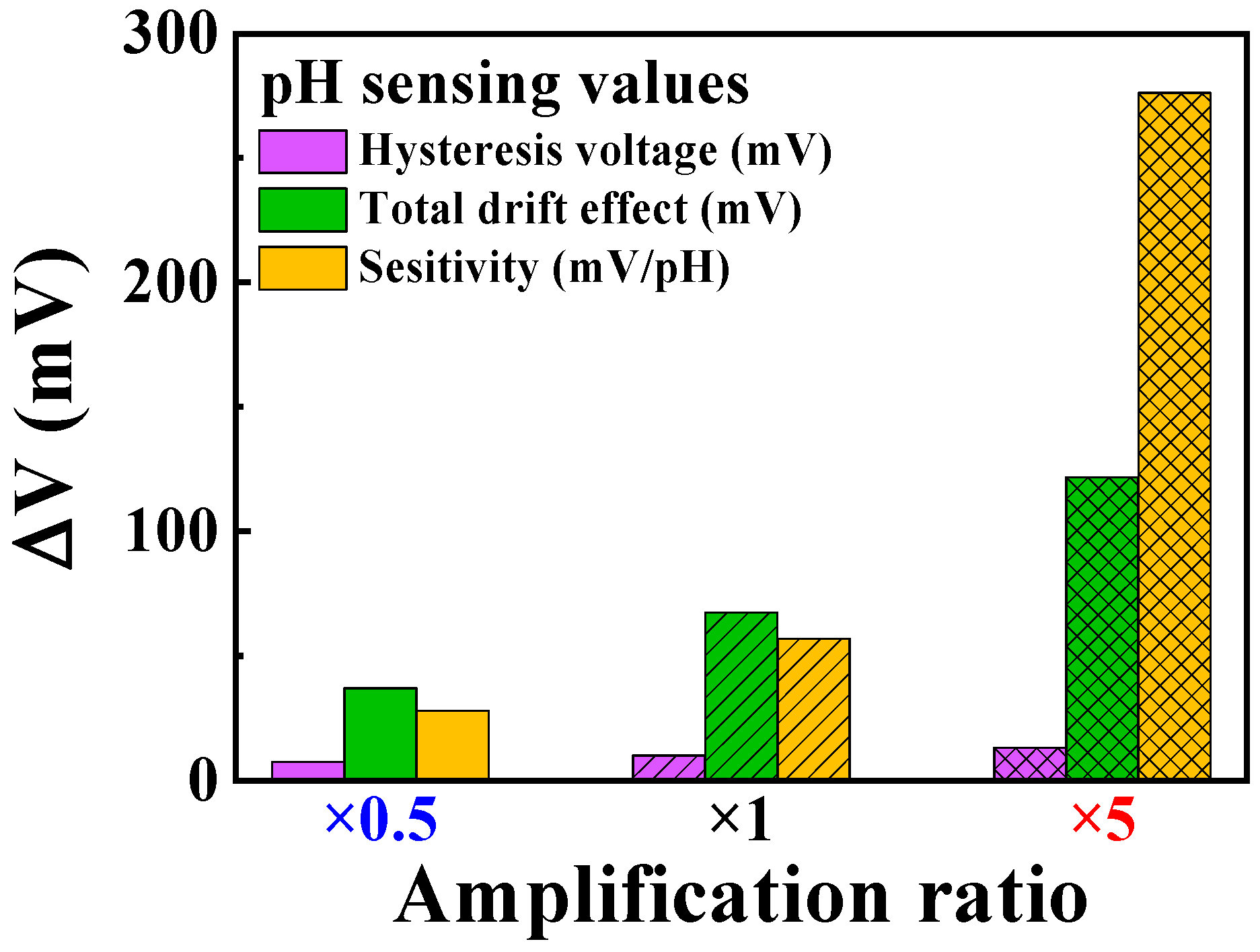
Table 2 summarizes the observed non-ideal effects and sensitivity values of the self-sensitivity programmable pH sensor platform based on the amplification ratios. As the amplification ratio increases, the numerical values of non-ideal effects also increase, seemingly indicating a decrease in the stability of the sensor platform. However, considering the increase in sensitivity, it can be noted that stability actually improves. Comparative data to confirm this are presented in Figure 10.
Figure 10 shows a quantitative comparison between the sensitivity and non-ideal effects in the pH-sensing operation. The parameters compared were sensitivity (ΔVREF per unit pH), total drift rate, and hysteresis voltage. Without amplification, ISFETs’ low sensitivity poses challenges as certain non-ideal effect values become larger than ΔVREF. This issue intensifies during prolonged measurements, rendering it difficult to discern whether ΔVREF variation is owing to pH differences or sensor platform instability. Consequently, accurate detection is impossible. Conversely, with the applied amplification, relatively accurate measurements are achievable owing to the significantly larger sensitivity values compared to the non-ideal effect values. This was quantitatively confirmed. The ratios of the hysteresis voltage to sensitivity were 26.19% at ×0.5 amplification, 17.52% at ×1 amplification, and 4.73% at ×5 amplification. Similarly, the ratios of the total drift effect to the sensitivity were 132.41% at ×0.5 amplification, 118.33% at ×1 amplification, and 44.12% at ×5 amplification, respectively.
The results demonstrated that, even after repetitive measurements of various pH values and continuous measurements for 10 h, the amplified sensitivity to unit pH was significantly larger than the total non-ideal effects. This indicates that the proposed sensor platform, with applied amplification, could accurately determine the pH of analytes, even in harsh environments. Therefore, the amplification ensured accurate and stable operational characteristics.
4. Conclusions
This study presents a novel pH sensor platform that leverages charge-trap-flash-type metal oxide semiconductor field-effect transistors (CTF-type MOSFETs) for enhanced sensitivity and self-amplification. Traditional ion-sensitive field-effect transistors (ISFETs) face challenges with commercialization due to low sensitivity at room temperature, known as the Nernst limit. To overcome this limitation, the research explores resistive coupling effects and CTF-type MOSFETs, enabling the flexible adjustment of the amplification ratio. The platform’s unique approach utilizes CTF-type MOSFETs as both transducers and resistors, allowing for efficient sensitivity control. To implement this, the electrical characteristics, energy band diagrams, and programmable resistance modulation of the CTF-type MOSFET are thoroughly characterized.
An extended-gate (EG) structure enhances cost-effectiveness and increases the sensor platform’s overall lifespan by preventing direct contact between analytes and the transducer. The proposed pH sensor platform demonstrates effective sensitivity control at various amplification ratios, showcasing stability and reliability even under repetitive and continuous operations. The key achievements of the study include the successful implementation of resistive coupling effects and CTF-type MOSFETs, enabling a multifunctional system with programmable sensitivity.
The results of sensitivity measurements demonstrate that the proposed self-sensitivity programmable pH sensor platform achieves amplification ratios very close to the intended ×0.5, ×1, ×5, with achieved amplification factors of approximately ×0.49 (28.02 mV/pH), ×1 (56.96 mV/pH), and ×4.85 (276.06 mV/pH), respectively. Further, the proposed sensor platform exhibits remarkable stability and reliability, as validated by the investigation of non-ideal effects such as hysteresis and drift.
The findings of this research contribute a robust and stable alternative for detecting micro-potential analytes, with promising applications in health management and point-of-care (PoC) settings. The ability to adjust sensitivity programmatically enhances the platform’s versatility, making it suitable for diverse environments and applications. Overall, the proposed pH sensor platform represents a significant advancement in the field of biosensors, paving the way for improved and reliable pH detection methodologies.
Author Contributions
Y.-U.K.: conceptualization, formal analysis, methodology, investigation, data curation, visualization, software, resources, and writing the original draft. W.-J.C.: conceptualization, methodology, investigation, resources, formal analysis, funding acquisition, supervision, validation, and writing the review & editing. All authors have read and agreed to the published version of the manuscript.
Funding
This work was supported by the Korea Institute for Advancement of Technology grant funded by the Korean government (MOTIE) (P0020967, The Competency Development Program for Industry Specialists).
Institutional Review Board Statement
Not applicable.
Informed Consent Statement
Not applicable.
Data Availability Statement
Data are contained within the article.
Acknowledgments
The present research has been conducted by the Research Grant of Kwangwoon University in 2023 and the excellent research support project of Kwangwoon University in 2023. The work reported in this paper was conducted during the sabbatical year of Kwangwoon University in 2023.
Conflicts of Interest
The authors declare no conflict of interest.
References
- Yager, P.; Domingo, G.J.; Gerdes, J. Point-of-Care Diagnostics for Global Health. Annu. Rev. Biomed. Eng. 2008, 10, 107–144. [Google Scholar] [CrossRef] [PubMed]
- Gubala, V.; Harris, L.F.; Ricco, A.J.; Tan, M.X.; Williams, D.E. Point of Care Diagnostics: Status and Future. Anal. Chem. 2012, 84, 487–515. [Google Scholar] [CrossRef] [PubMed]
- Biswas, G.C.; Choudhury, S.; Rabbani, M.M.; Das, J. A Review on Potential Electrochemical Point-of-Care Tests Targeting Pandemic Infectious Disease Detection: COVID-19 as a Reference. Chemosensors 2022, 10, 269. [Google Scholar] [CrossRef]
- Kumar, A.; Parihar, A.; Panda, U.; Parihar, D.S. Microfluidics-Based Point-of-Care Testing (POCT) Devices in Dealing with Waves of COVID-19 Pandemic: The Emerging Solution. ACS Appl. Bio Mater. 2021, 5, 2046–2068. [Google Scholar] [CrossRef] [PubMed]
- Goicoechea, J.; Zamarreño, C.R.; Matías, I.R.; Arregui, F.J. Optical Fiber PH Sensors Based on Layer-by-Layer Electrostatic Self-Assembled Neutral Red. Sens. Actuators B Chem. 2008, 132, 305–311. [Google Scholar] [CrossRef]
- Lin, J. Recent Development and Applications of Optical and Fiber-Optic PH Sensors. TrAC Trends Anal. Chem. 2000, 19, 541–552. [Google Scholar] [CrossRef]
- Szmacinski, H.; Lakowicz, J.R. Optical Measurements of PH Using Fluorescence Lifetimes and Phase-Modulation Fluorometry. Anal. Chem. 1993, 65, 1668–1674. [Google Scholar] [CrossRef] [PubMed]
- Qi, J.; Liu, D.; Liu, X.; Guan, S.; Shi, F.; Chang, H.; He, H.; Yang, G. Fluorescent PH Sensors for Broad-Range PH Measurement Based on a Single Fluorophore. Anal. Chem. 2015, 87, 5897–5904. [Google Scholar] [CrossRef]
- Pijanowska, D.G.; Torbicz, W. PH-ISFET Based Urea Biosensor. Sens. Actuators B Chem. 1997, 44, 370–376. [Google Scholar] [CrossRef]
- Cai, Q.; Zeng, K.; Ruan, C.; Desai, T.A.; Grimes, C.A. A Wireless, Remote Query Glucose Biosensor Based on a PH-Sensitive Polymer. Anal. Chem. 2004, 76, 4038–4043. [Google Scholar] [CrossRef]
- Moser, N.; Lande, T.S.; Toumazou, C.; Georgiou, P. ISFETs in CMOS and Emergent Trends in Instrumentation: A Review. IEEE Sens. J. 2016, 16, 6496–6514. [Google Scholar] [CrossRef]
- Douthwaite, M.; Moser, N.; Georgiou, P. CMOS ISFET Arrays for Integrated Electrochemical Sensing and Imaging Applications: A Tutorial. IEEE Sens. J. 2021, 21, 22155–22169. [Google Scholar] [CrossRef]
- Wong, H.S.; White, M.H. A Cmos-Integrated “Isfet-Operational Amplifier” Chemical Sensor Employing Differential Sensing. IEEE Trans. Electron Devices 1989, 36, 479–487. [Google Scholar] [CrossRef]
- Chan, W.P.; Premanode, B.; Toumazou, C. An Integrated ISFETs Instrumentation System in Standard CMOS Technology. IEEE J. Solid-State Circuits 2010, 45, 1923–1934. [Google Scholar] [CrossRef]
- Bergveld, P. The Operation of an ISFET as an Electronic Device. Sens. Actuators 1981, 1, 17–29. [Google Scholar] [CrossRef]
- Knopfmacher, O.; Tarasov, A.; Fu, W.; Wipf, M.; Niesen, B.; Calame, M.; Schönenberger, C. Nernst Limit in Dual-Gated Si-Nanowire FET Sensors. Nano Lett. 2010, 10, 2268–2274. [Google Scholar] [CrossRef] [PubMed]
- Bergveld, P. Thirty Years of ISFETOLOGY: What Happened in the Past 30 Years and What May Happen in the next 30 Years. Sens. Actuators B Chem. 2003, 88, 1–20. [Google Scholar] [CrossRef]
- Cho, S.-K.; Cho, W.-J. High-Sensitivity PH Sensor Based on Coplanar Gate AlGaN/GaN Metal-Oxide-Semiconductor High Electron Mobility Transistor. Chemosensors 2021, 9, 42. [Google Scholar] [CrossRef]
- Shojaei Baghini, M.; Vilouras, A.; Douthwaite, M.; Georgiou, P.; Dahiya, R. Ultra-Thin ISFET-Based Sensing Systems. Electrochem. Sci. Adv. 2022, 2, e2100202. [Google Scholar] [CrossRef]
- Ahn, J.H.; Kim, J.Y.; Seol, M.L.; Baek, D.J.; Guo, Z.; Kim, C.H.; Choi, S.J.; Choi, Y.K. A PH Sensor with a Double-Gate Silicon Nanowire Field-Effect Transistor. Appl. Phys. Lett. 2013, 102, 83701. [Google Scholar] [CrossRef]
- Livingstone, A.W.; Welbourn, A.D.; Blau, G.L. Manufacturing Tolerance of Capacitor Coupled GaAs FET Logic Circuits. IEEE Electron Device Lett. 1982, 3, 284–285. [Google Scholar] [CrossRef]
- Xu, C.; Banerjee, K. Physical Modeling of the Capacitance and Capacitive Coupling Noise of through-Oxide vias in FDSOI-Based Ultra-High Density 3-D ICs. IEEE Trans. Electron Devices 2013, 60, 123–131. [Google Scholar] [CrossRef]
- Shin, K.; Kang, D.S.; Lee, S.H.; Moon, W. A Scanning Microscopy Technique Based on Capacitive Coupling with a Field-Effect Transistor Integrated with the Tip. Ultramicroscopy 2015, 159, 1–10. [Google Scholar] [CrossRef]
- Jang, K.H.; Jang, H.J.; Park, J.K.; Cho, W.J. Self-Amplified Dual Gate Charge Trap Flash Memory for Low-Voltage Operation. IEEE Electron Device Lett. 2013, 34, 756–758. [Google Scholar] [CrossRef]
- Ahn, M.J.; Cho, W.J. Dual-Gate Charge Trap Flash Memory for Highly Reliable Triple Level Cell Using Capacitive Coupling Effects. IEEE Electron Device Lett. 2017, 38, 36–39. [Google Scholar] [CrossRef]
- Kim, M.; Park, E.; Kim, I.S.; Park, J.; Kim, J.; Jeong, Y.; Lee, S.; Kim, I.; Park, J.K.; Seong, T.Y.; et al. A Comparison Study on Multilayered Barrier Oxide Structure in Charge Trap Flash for Synaptic Operation. Crystals 2021, 11, 70. [Google Scholar] [CrossRef]
- Yin, L.T.; Chou, J.C.; Chung, W.Y.; Sun, T.P.; Hsiung, S.K. Separate Structure Extended Gate H+-Ion Sensitive Field Effect Transistor on a Glass Substrate. Sens. Actuators B Chem. 2000, 71, 106–111. [Google Scholar] [CrossRef]
- Chi, L.L.; Chou, J.C.; Chung, W.Y.; Sun, T.P.; Hsiung, S.K. Study on Extended Gate Field Effect Transistor with Tin Oxide Sensing Membrane. Mater. Chem. Phys. 2000, 63, 19–23. [Google Scholar] [CrossRef]
- Yin, L.T.; Chou, J.C.; Chung, W.Y.; Sun, T.P.; Hsiung, S.K. Study of Indium Tin Oxide Thin Film for Separative Extended Gate ISFET. Mater. Chem. Phys. 2001, 70, 12–16. [Google Scholar] [CrossRef]
- Chou, J.C.; Wang, Y.F. Preparation and Study on the Drift and Hysteresis Properties of the Tin Oxide Gate ISFET by the Sol–Gel Method. Sens. Actuators B Chem. 2002, 86, 58–62. [Google Scholar] [CrossRef]
- Tsai, C.N.; Chou, J.C.; Sun, T.P.; Hsiung, S.K. Study on the Sensing Characteristics and Hysteresis Effect of the Tin Oxide PH Electrode. Sens. Actuators B Chem. 2005, 108, 877–882. [Google Scholar] [CrossRef]
- Jamasb, S. An Analytical Technique for Counteracting Drift in Ion-Selective Field Effect Transistors (ISFETs). IEEE Sens. J. 2004, 4, 795–801. [Google Scholar] [CrossRef]
- Chen, D.Y.; Chan, P.K. An Intelligent ISFET Sensory System with Temperature and Drift Compensation for Long-Term Monitoring. IEEE Sens. J. 2008, 8, 1948–1959. [Google Scholar] [CrossRef]
- Bousse, L.; van den Vlekkert, H.H.; de Rooij, N.F. Hysteresis in Al2O3-Gate ISFETs. Sens. Actuators B Chem. 1990, 2, 103–110. [Google Scholar] [CrossRef]
- Trinh, T.T.; Nguyen, V.D.; Ryu, K.; Jang, K.; Lee, W.; Baek, S.; Raja, J.; Yi, J. Improvement in the Performance of an InGaZnO Thin-Film Transistor by Controlling Interface Trap Densities between the Insulator and Active Layer. Semicond. Sci. Technol. 2011, 26, 085012. [Google Scholar] [CrossRef]
- Du, H.; Lin, X.; Xu, Z.; Chu, D. Electric Double-Layer Transistors: A Review of Recent Progress. J. Mater. Sci. 2015, 50, 5641–5673. [Google Scholar] [CrossRef]
- Lee, D.H.; Park, H.; Cho, W.J. Advancements in Complementary Metal-Oxide Semiconductor-Compatible Tunnel Barrier Engineered Charge-Trapping Synaptic Transistors for Bio-Inspired Neural Networks in Harsh Environments. Biomimetics 2023, 8, 506. [Google Scholar] [CrossRef]
- Baik, S.J.; Shin, H. Charge Trapping in Amorphous Dielectrics for Secure Charge Storage. ACS Appl. Mater. Interfaces 2021, 13, 11507–11514. [Google Scholar] [CrossRef]
- Hota, M.K.; Alshammari, F.H.; Salama, K.N.; Alshareef, H.N. Transparent Flash Memory Using Single Ta2O5 Layer for Both Charge-Trapping and Tunneling Dielectrics. ACS Appl. Mater. Interfaces 2017, 9, 21856–21863. [Google Scholar] [CrossRef]
- Nakata, S.; Saito, K.; Shimada, M. Non-Volatile Al2O3 Memory Using Nanoscale Al-Rich Al2O3 Thin Film as a Charge Storage Layer. Jpn. J. Appl. Phys. Part 1 Regul. Pap. Short. Notes Rev. Pap. 2006, 45, 3176–3178. [Google Scholar] [CrossRef]
- Lee, D.J.; Yim, S.S.; Kim, K.S.; Kim, S.H.; Kim, K.B. Nonvolatile Memory Characteristics of Atomic Layer Deposited Ru Nanocrystals with a SiO2/Al2O3 Bilayered Tunnel Barrier. J. Appl. Phys. 2010, 107, 13707. [Google Scholar] [CrossRef]
- Kim, H.J.; Cha, S.Y.; Choi, D.J. Memory Characteristics of Al2O3/La2O3/Al2O3 Multi-Layer Films with Various Blocking and Tunnel Oxide Thicknesses. Mater. Sci. Semicond. Process 2010, 13, 9–12. [Google Scholar] [CrossRef]
- Zhu, W.J.; Ma, T.P.; Zafar, S.; Tamagawa, T. Charge Trapping in Ultrathin Hafnium Oxide. IEEE Electron Device Lett. 2002, 23, 597–599. [Google Scholar] [CrossRef]
- Maikap, S.; Lee, H.Y.; Wang, T.Y.; Tzeng, P.J.; Wang, C.C.; Lee, L.S.; Liu, K.C.; Yang, J.R.; Tsai, M.J. Charge Trapping Characteristics of Atomic-Layer-Deposited HfO2 Films with Al2O3 as a Blocking Oxide for High-Density Non-Volatile Memory Device Applications. Semicond. Sci. Technol. 2007, 22, 884. [Google Scholar] [CrossRef]
- Song, Y.S.; Song, Y.S.; Jang, T.; Min, K.K.; Baek, M.H.; Yu, J.; Kim, Y.; Lee, J.H.; Park, B.G. Tunneling Oxide Engineering for Improving Retention in Nonvolatile Charge-Trapping Memory with TaN/Al2O3/HfO2/SiO2/Al2O3/SiO2/Si Structure. Jpn. J. Appl. Phys. 2020, 59, 061006. [Google Scholar] [CrossRef]
- Yoo, J.H.; Park, W.J.; Kim, S.W.; Lee, G.R.; Kim, J.H.; Lee, J.H.; Uhm, S.H.; Lee, H.C. Preparation of Remote Plasma Atomic Layer-Deposited HfO2 Thin Films with High Charge Trapping Densities and Their Application in Nonvolatile Memory Devices. Nanomaterials 2023, 13, 1785. [Google Scholar] [CrossRef]
- Yoon, G.; Kim, T.; Agrawal, K.; Kim, J.; Park, J.; Kim, H.-H.; Cho, E.-C.; Yi, J. Optimization of MIS Type Non-Volatile Memory Device with Al-Doped HfO2 as Charge Trapping Layer. ECS J. Solid State Sci. Technol. 2020, 9, 075004. [Google Scholar] [CrossRef]
- Govoreanu, B.; Blomme, P.; Rosmeulen, M.; Van Houdt, J.; De Meyer, K. Variot: A Novel Multilayer Tunnel Barrier Concept for Low-Voltage Nonvolatile Memory Devices. IEEE Electron Device Lett. 2003, 24, 99–101. [Google Scholar] [CrossRef]
- Spitzer, A.; Baunach, R. The Physics of ONO Layer Dielectrics. Appl. Surf. Sci. 1989, 39, 192–199. [Google Scholar] [CrossRef]
- Golubović, D.S.; Vianello, E.; Arreghini, A.; Driussi, F.; Van Duuren, M.J.; Akil, N.; Selmi, L.; Esseni, D. Programme and Retention Characteristics of SONOS Memory Arrays with Layered Tunnel Barrier. Semicond. Sci. Technol. 2008, 23, 075003. [Google Scholar] [CrossRef]
- Lu, C.Y.; Hsieh, K.Y.; Liu, R. Future Challenges of Flash Memory Technologies. Microelectron. Eng. 2009, 86, 283–286. [Google Scholar] [CrossRef]
- Mori, S.; Sakagami, E.; Araki, H.; Kaneko, Y.; Narita, K.; Ohshima, Y.; Yoshikawa, K.; Arai, N. ONO Inter-Poly Dielectric Scaling for Nonvolatile Memory Applications. IEEE Trans. Electron Devices 1991, 38, 386–391. [Google Scholar] [CrossRef]
- Boutchich, M.; Golubović, D.S.; Akil, N.; van Duuren, M. Evaluation of Layered Tunnel Barrier Charge Trapping Devices for Embedded Non-Volatile Memories. Microelectron. Eng. 2010, 87, 41–46. [Google Scholar] [CrossRef]
- Mori, S.; Araki, Y.Y.; Sato, M.; Meguro, H.; Tsunoda, H.; Kamiya, E.; Yoshikawa, K.; Arai, N.; Sakagami, E. Thickness Scaling Limitation Factors of ONO Interpoly Dielectric for Nonvolatile Memory Devices. IEEE Trans. Electron Devices 1996, 43, 47–53. [Google Scholar] [CrossRef]
- Kobayashi, K.; Miyatake, H.; Hirayama, M.; Higaki, T.; Abe, H. Dielectric Breakdown and Current Conduction of Oxide/Nitride/Oxide Multi-Layer Structures. J. Electrochem. Soc. 1992, 139, 1693–1699. [Google Scholar] [CrossRef]
- Mori, S.; Kaneko, Y.; Yoshikawa, K.; Arai, N. Polyoxide Thinning Limitation and Superior ONO Interpoly Dielectric for Nonvolatile Memory Devices. IEEE Trans. Electron Devices 1991, 38, 270–277. [Google Scholar] [CrossRef]
- Mielke, N.; Belgal, H.; Kalastirsky, I.; Kalavade, P.; Kurtz, A.; Meng, Q.; Righos, N.; Wu, J. Flash EEPROM Threshold Instabilities Due to Charge Trapping during Program/Erase Cycling. IEEE Trans. Device Mater. Reliab. 2004, 4, 335–343. [Google Scholar] [CrossRef]
- Min, J.; Ronchi, N.; McMitchell, S.R.C.; OrSullivan, B.; Banerjee, K.; Van den Bosch, G.; Van Houdt, J.; Shin, C. Program/Erase Scheme for Suppressing Interface Trap Generation in HfO2-Based Ferroelectric Field Effect Transistor. IEEE Electron Device Lett. 2021, 42, 1280–1283. [Google Scholar] [CrossRef]
- Kim, D.H.; Park, B.G. Program/Erase Model of NAND-Type Nitride-Based Charge Trapping Flash Memories. In Proceedings of the IEEE 2008 Silicon Nanoelectronics Workshop, Honolulu, HI, USA, 15–16 June 2008. [Google Scholar] [CrossRef]
- Kim, S.J.; Lee, S.Y.; Lee, Y.W.; Kuk, S.H.; Kwon, J.Y.; Han, M.K. Effect of Charge Trapping/Detrapping on Threshold Voltage Shift of IGZO TFTs under AC Bias Stress. Electrochem. Solid-State Lett. 2012, 15, H108–H110. [Google Scholar] [CrossRef]
- Zafar, S.; Callegari, A.; Gusev, E.; Fischetti, M.V. Charge Trapping Related Threshold Voltage Instabilities in High Permittivity Gate Dielectric Stacks. J. Appl. Phys. 2003, 93, 9298–9303. [Google Scholar] [CrossRef]
- Zafar, S.; Callegari, A.; Gusev, E.; Fischetti, M.V. Charge Trapping in High K Gate Dielectric Stacks. Tech. Dig. Int. Electron Devices Meet. 2002, 517–520. [Google Scholar] [CrossRef]
- Liu, J.; Jaiyen, B.; Kim, Y.; Wilkerson, C.; Mutlu, O. MutluOnur An Experimental Study of Data Retention Behavior in Modern DRAM Devices. ACM SIGARCH Comput. Archit. News 2013, 41, 60–71. [Google Scholar] [CrossRef]
- Tao, G.; Scarpa, A.; Dijkstra, J.; Stidl, W.; Kuper, F. Data Retention Prediction for Modern Floating Gate Non-Volatile Memories. Microelectron. Reliab. 2000, 40, 1561–1566. [Google Scholar] [CrossRef]
- Krieger, J.H.; Spitzer, S.M. Non-Traditional, Non-Volatile Memory Based on Switching and Retention Phenomena in Polymeric Thin Films. In Proceedings of the 2004 Non-Volatile Memory Technology Symposium, NVMTS, Orlando, FL, USA, 17 November 2004; pp. 121–124. [Google Scholar] [CrossRef]
- Jamasb, S.; Collins, S.; Smith, R.L. A Physical Model for Drift in PH ISFETs. Sens. Actuators B Chem. 1998, 49, 146–155. [Google Scholar] [CrossRef]
- Chou, J.C.; Weng, C.Y. Sensitivity and Hysteresis Effect in Al2O3 Gate PH-ISFET. Mater. Chem. Phys. 2001, 71, 120–124. [Google Scholar] [CrossRef]
- Chiang, J.L.; Jan, S.S.; Chou, J.C.; Chen, Y.C. Study on the Temperature Effect, Hysteresis and Drift of PH-ISFET Devices Based on Amorphous Tungsten Oxide. Sens. Actuators B Chem. 2001, 76, 624–628. [Google Scholar] [CrossRef]
Figure 1.
(a) Optical microscope image and (b) schematic structure with a cross-sectional view of the thin-film layers of the CTF-type MOSFET.
Figure 1.
(a) Optical microscope image and (b) schematic structure with a cross-sectional view of the thin-film layers of the CTF-type MOSFET.
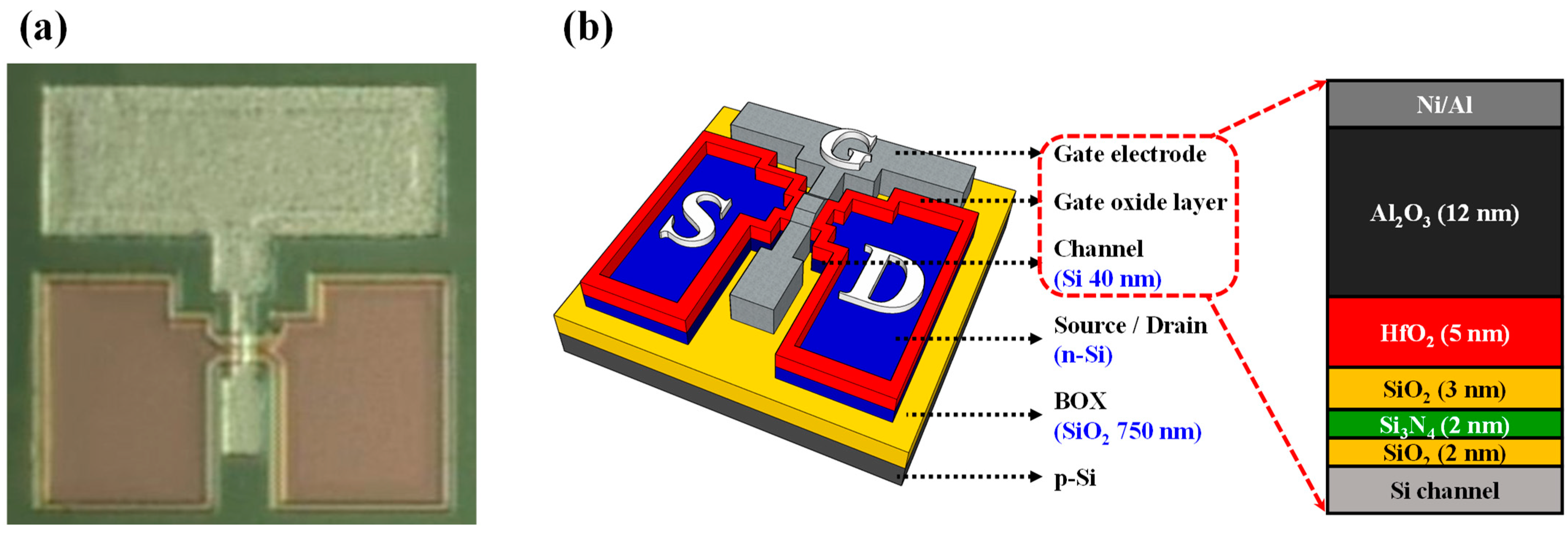
Figure 2.
Simplified equivalent circuit for the self-sensitivity programmable pH sensor platform.
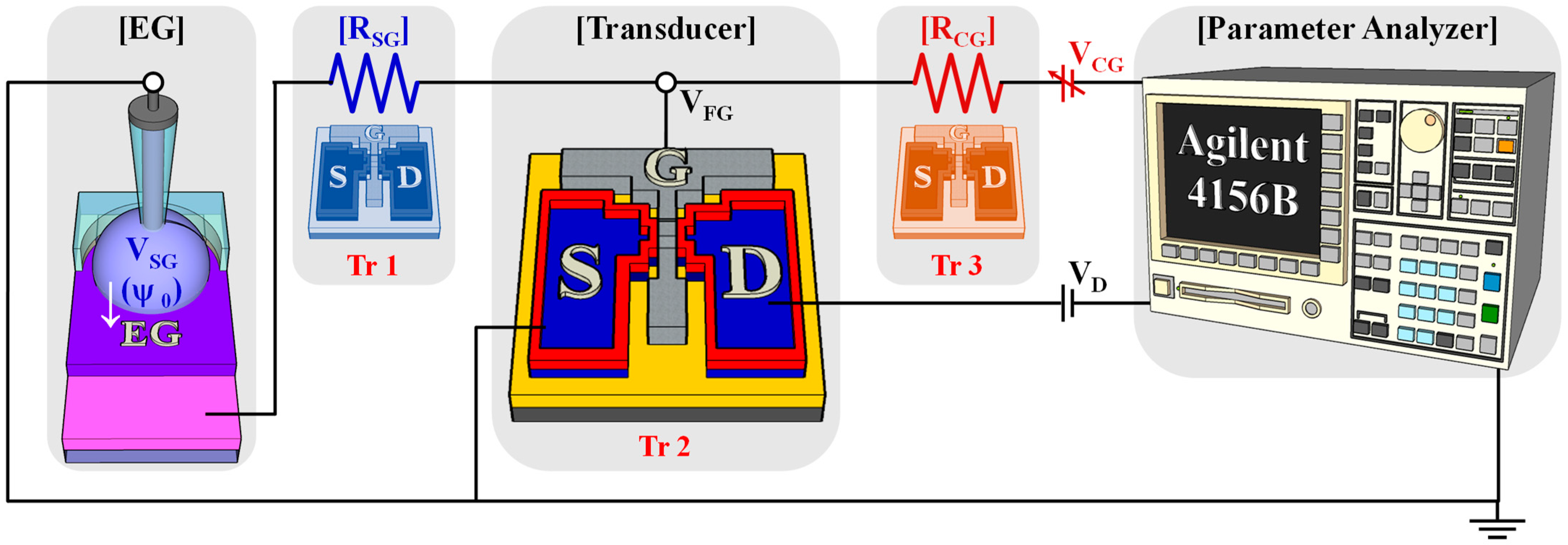
Figure 3.
Electrical characteristics of CTF-type MOSFET: (a) transfer curve, and (b) output curve.
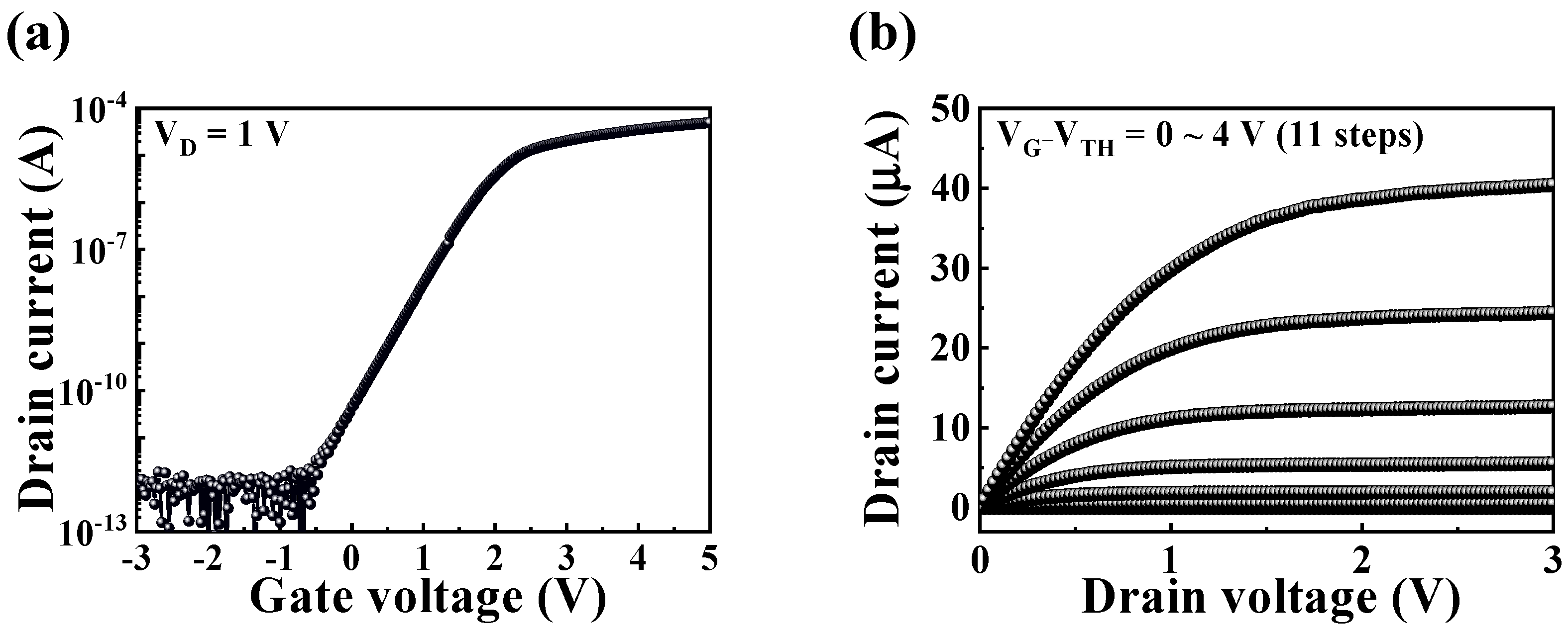
Figure 4.
Energy band diagram of CTF-type MOSFET under (a) non-bias, (b) positive-bias, and (c) negative-bias states.
Figure 4.
Energy band diagram of CTF-type MOSFET under (a) non-bias, (b) positive-bias, and (c) negative-bias states.

Figure 5.
(a) Transfer curves, (b) hysteresis resistance, and (c) retention time according to the program/erasure modes.
Figure 5.
(a) Transfer curves, (b) hysteresis resistance, and (c) retention time according to the program/erasure modes.

Figure 6.
Channel resistance modulation with input pulse application. Conditions include the number of pulses: (a) 1, (b) 10, and (c) 50.
Figure 6.
Channel resistance modulation with input pulse application. Conditions include the number of pulses: (a) 1, (b) 10, and (c) 50.

Figure 7.
pH sensing operation of self-sensitivity programmable pH sensor with amplification ratio of (a) ×0.5, (b) ×1, and (c) ×5.
Figure 7.
pH sensing operation of self-sensitivity programmable pH sensor with amplification ratio of (a) ×0.5, (b) ×1, and (c) ×5.

Figure 8.
Programmed pH sensitivity values based on the amplification ratio.

Figure 9.
Non-ideal effect of the self-sensitivity programmable pH sensor platform: (a) hysteresis voltage, and (b) drift rate.
Figure 9.
Non-ideal effect of the self-sensitivity programmable pH sensor platform: (a) hysteresis voltage, and (b) drift rate.
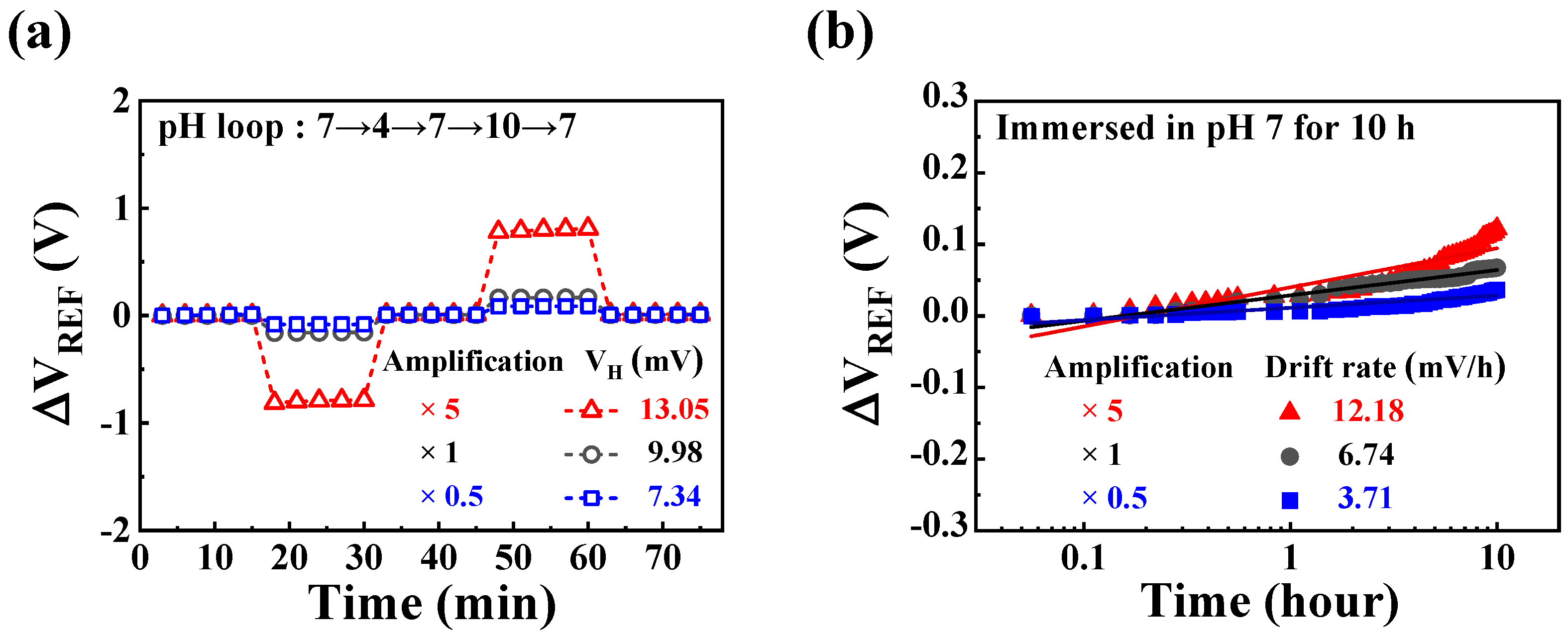
Figure 10.
Comparative analysis of sensitivity and non-ideal effects in pH sensing operations.

Table 1.
Electrical parameters of the multi-functional CTF-type MOSFET.
| VTH (V) | SS (mV/dec) | μFE (cm2/V·s) | Ion/Ioff (A/A) |
|---|---|---|---|
| −0.25 | 175.54 | 234.92 | 1.49 × 10⁷ |
Table 2.
Summarization of non-ideal effects and sensitivity values of the self-sensitivity programmable pH sensor platform according to the amplification ratio.
Table 2.
Summarization of non-ideal effects and sensitivity values of the self-sensitivity programmable pH sensor platform according to the amplification ratio.
| Amplification Ratio | Hysteresis Voltage (mV) | Drift Rate (mV/h) | Sensitivity (mV/pH) |
|---|---|---|---|
| ×0.5 | 7.34 | 3.71 | 28.02 |
| ×1 | 9.98 | 6.74 | 56.96 |
| ×5 | 13.05 | 12.18 | 276.06 |
Disclaimer/Publisher’s Note: The statements, opinions and data contained in all publications are solely those of the individual author(s) and contributor(s) and not of MDPI and/or the editor(s). MDPI and/or the editor(s) disclaim responsibility for any injury to people or property resulting from any ideas, methods, instructions or products referred to in the content. |
© 2024 by the authors. Licensee MDPI, Basel, Switzerland. This article is an open access article distributed under the terms and conditions of the Creative Commons Attribution (CC BY) license (https://creativecommons.org/licenses/by/4.0/).
Share and Cite
MDPI and ACS Style
Kim, Y.-U.; Cho, W.-J. Smart pH Sensing: A Self-Sensitivity Programmable Platform with Multi-Functional Charge-Trap-Flash ISFET Technology. Sensors 2024, 24, 1017. https://doi.org/10.3390/s24031017
AMA Style
Kim Y-U, Cho W-J. Smart pH Sensing: A Self-Sensitivity Programmable Platform with Multi-Functional Charge-Trap-Flash ISFET Technology. Sensors. 2024; 24(3):1017. https://doi.org/10.3390/s24031017
Chicago/Turabian StyleKim, Yeong-Ung, and Won-Ju Cho. 2024. "Smart pH Sensing: A Self-Sensitivity Programmable Platform with Multi-Functional Charge-Trap-Flash ISFET Technology" Sensors 24, no. 3: 1017. https://doi.org/10.3390/s24031017
Note that from the first issue of 2016, this journal uses article numbers instead of page numbers. See further details here.