
Wideband MOEMS for the Calibration of Optical Readout Systems

 ,
, 
Abstract
:1. Introduction
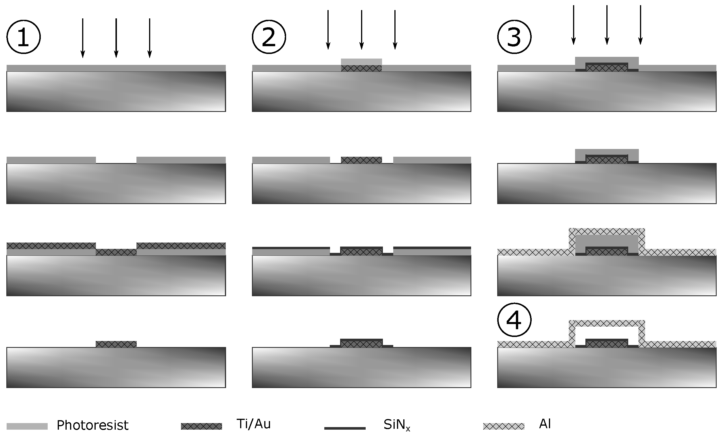
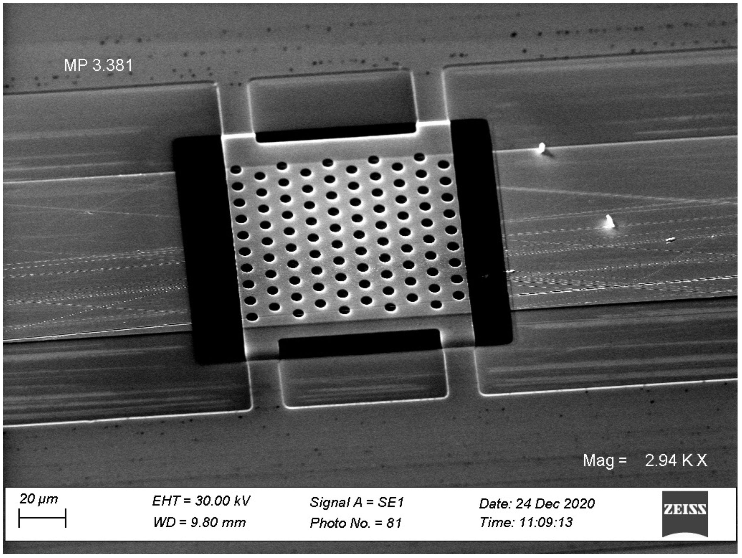
2. Technology
- the formation of a bottom electrode;
- the formation of a layer of the protective dielectric;
- the formation of the membrane;
- the release of the membrane.
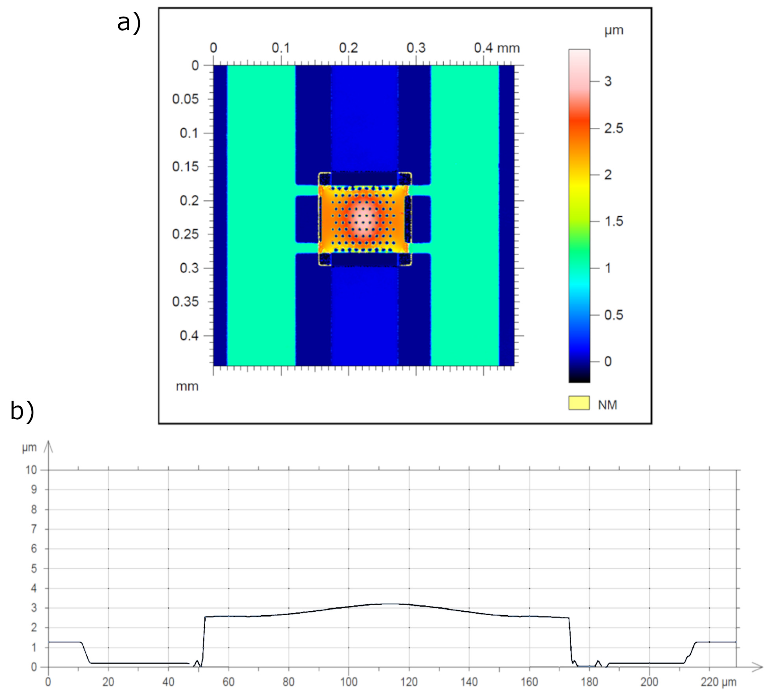
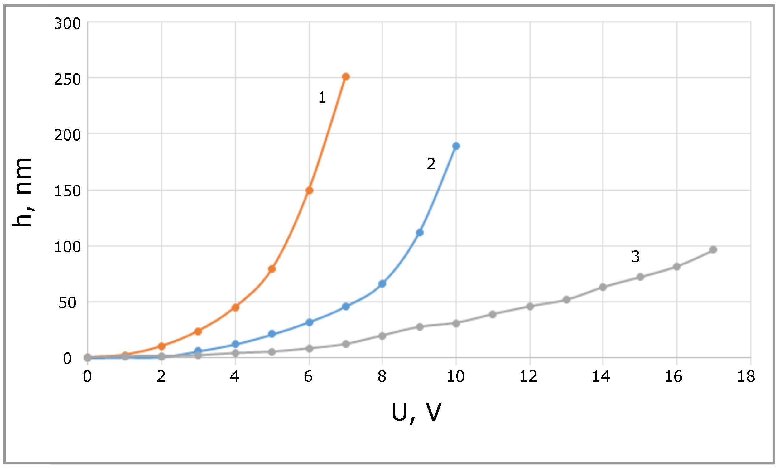
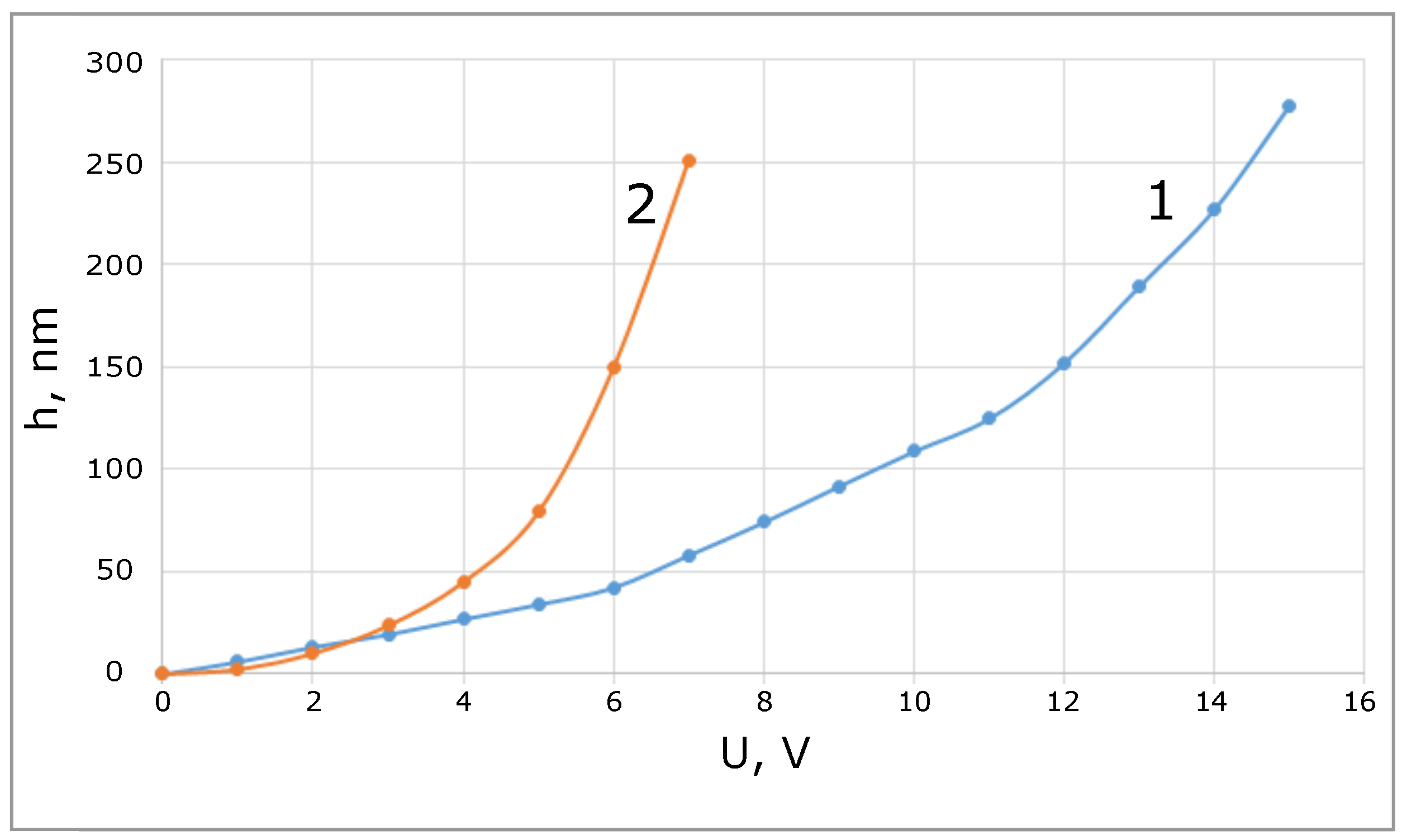
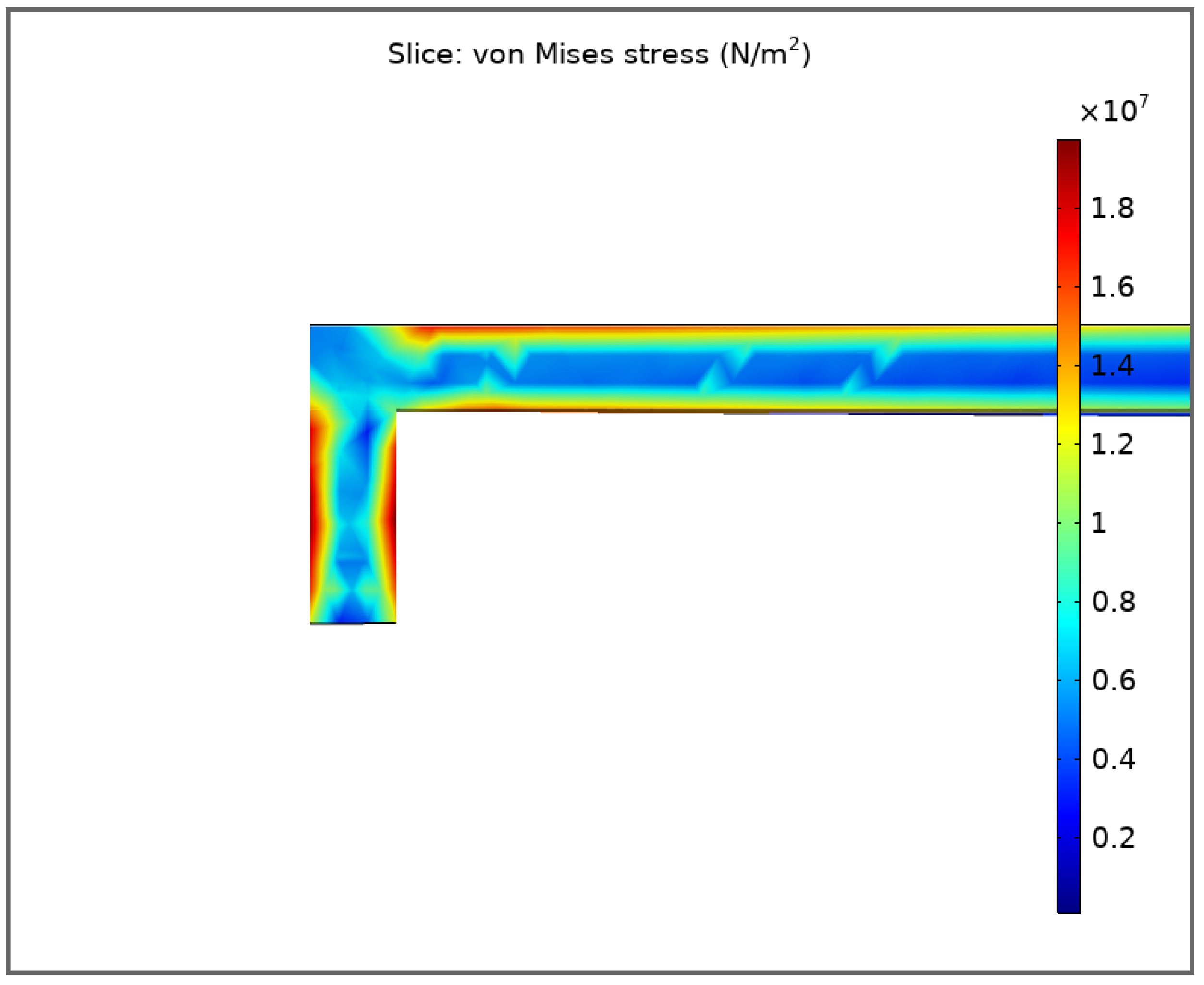
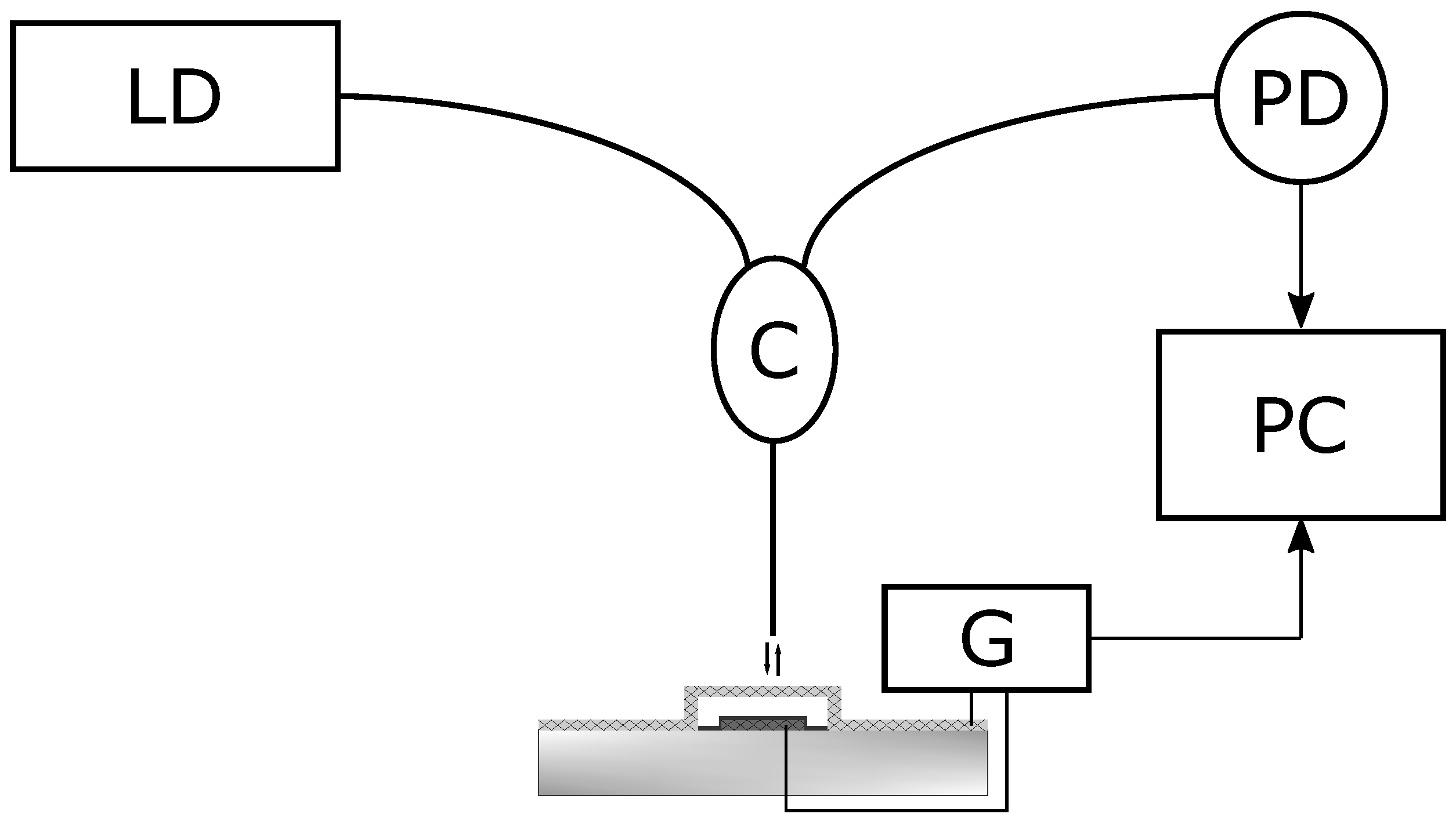
3. Studying Static Parameters
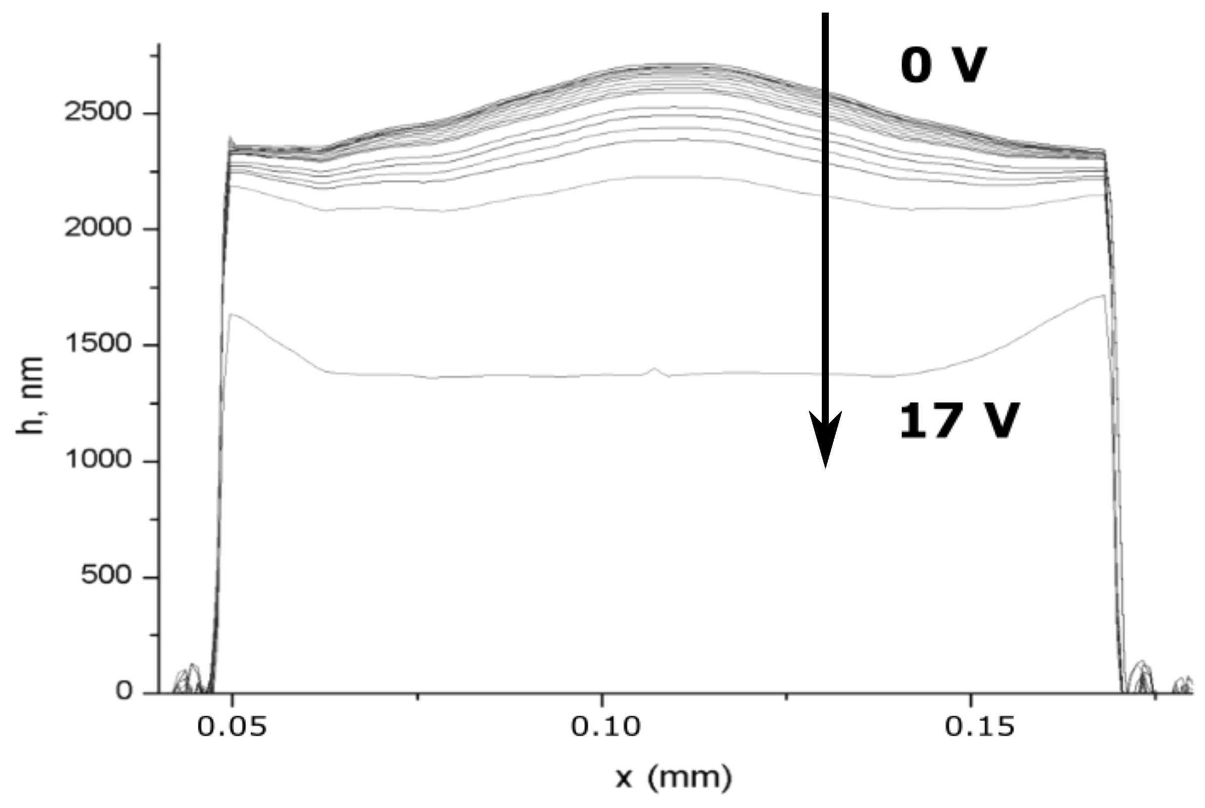
4. Dynamic Parameters
5. Conclusions
Author Contributions
Funding
Institutional Review Board Statement
Informed Consent Statement
Data Availability Statement
Acknowledgments
Conflicts of Interest
References
- Verma, P.; Khan, K.Z.; Khonina, S.N.; Kazanskiy, N.L.; Gopal, R. Ultraviolet-LIGA-based fabrication and characterization of a nonresonant drive-mode vibratory gyro/accelerometer. J. Micro/Nanolithogr. MEMS MOEMS 2016, 15, 1–9. [Google Scholar] [CrossRef]
- Jangra, M.; Arya, D.S.; Khosla, R.; Sharma, S.K. Maskless lithography: An approach to SU-8 based sensitive and high-g Z-axis polymer MEMS accelerometer. Microsyst. Technol. 2021, 27, 2925–2934. [Google Scholar] [CrossRef]
- Han, J.; Zhu, Y.; Tao, G.; Zhao, Z.; Yin, Y.; Niu, W.; Dong, L. A Triaxial Accelerometer Based on Differential Resonant Beams and Force-Balanced Capacitive Plates. IEEE Sens. J. 2019, 19, 6602–6609. [Google Scholar] [CrossRef]
- Bruno, F.A.; Pisco, M.; Gruca, G.; Rijnveld, N.; Cusano, A. Opto-Mechanical Lab-on-Fiber Accelerometers. J. Light. Technol. 2020, 38, 1998–2009. [Google Scholar] [CrossRef]
- Aspelmeyer, M.; Kippenberg, T.J.; Marquardt, F. Cavity optomechanics. Rev. Mod. Phys. 2014, 86, 1391–1452. [Google Scholar] [CrossRef]
- Metcalfe, M. Applications of cavity optomechanics. Appl. Phys. Rev. 2014, 1, 031105. [Google Scholar] [CrossRef]
- Iannuzzi, D.; Deladi, S.; Gadgil, V.J.; Sanders, R.G.P.; Schreuders, H.; Elwenspoek, M.C. Monolithic fiber-top sensor for critical environments and standard applications. Appl. Phys. Lett. 2006, 88, 053501. [Google Scholar] [CrossRef] [Green Version]
- Li, M.; Wang, M.; Li, H. Optical MEMS pressure sensor based on Fabry-Perot interferometry. Opt. Express 2006, 14, 1497–1504. [Google Scholar] [CrossRef]
- Pang, C.; Bae, H.; Gupta, A.; Bryden, K.; Yu, M. MEMS Fabry-Perot sensor interrogated by optical system-on-a-chip for simultaneous pressure and temperature sensing. Opt. Express 2013, 21, 21829–21839. [Google Scholar] [CrossRef] [PubMed]
- Ge, Y.; Wang, M.; Yan, H. Optical MEMS pressure sensor based on a mesa-diaphragm structure. Opt. Express 2008, 16, 21746–21752. [Google Scholar] [CrossRef]
- Javernik, A.; Donlagic, D. Miniature, micro-machined, fiber-optic Fabry-Perot voltage sensor. Opt. Express 2019, 27, 13280–13291. [Google Scholar] [CrossRef]
- Stievater, T.H.; Rabinovich, W.S.; Ferraro, M.S.; Papanicolaou, N.A.; Bass, R.; Boos, J.B.; Stepnowski, J.L.; McGill, R.A. Photonic microharp chemical sensors. Opt. Express 2008, 16, 2423–2430. [Google Scholar] [CrossRef] [PubMed]
- Teixeira, J.G.V.; Leite, I.T.; Silva, S.; Frazão, O. Advanced fiber-optic acoustic sensors. Photonic Sens. 2014, 4, 198–208. [Google Scholar] [CrossRef] [Green Version]
- Ishihara, K.; Yung, C.F.; Ayon, A.; Schmidt, M. Inertial sensor technology using DRIE and wafer bonding with connecting capability. J. Microelectromech. Syst. 1999, 8, 403–408. [Google Scholar] [CrossRef]
- Li, Z.; Yang, Z.; Xiao, Z.; Hao, Y.; Li, T.; Wu, G.; Wang, Y. A bulk micromachined vibratory lateral gyroscope fabricated with wafer bonding and deep trench etching. Sens. Actuators A Phys. 2000, 83, 24–29. [Google Scholar] [CrossRef]
- Li, B.; Li, C.; Zhao, Y.; Han, C.; Zhang, Q. Deep Reactive Ion Etching of Z-Cut Alpha Quartz for MEMS Resonant Devices Fabrication. Micromachines 2020, 11, 724. [Google Scholar] [CrossRef]
- Oh, Y.; Lee, B.; Baek, S.; Kim, H.; Kim, J.; Kang, S.; Song, C. A surface-micromachined tunable vibratory gyroscope. In Proceedings of the IEEE the Tenth Annual International Workshop on Micro Electro Mechanical Systems, An Investigation of Micro Structures, Sensors, Actuators, Machines and Robots, Nagoya, Japan, 26–30 January 1997; pp. 272–277. [Google Scholar] [CrossRef]
- Piljek, P.; Keran, Z.; Math, M. Micromachining. Interdiscip. Descr. Complex Syst. 2014, 12, 1–27. [Google Scholar] [CrossRef]
- Shin, E.; Yeo, H.G.; Yeon, A.; Jin, C.; Park, W.; Lee, S.C.; Choi, H. Development of a High-Density Piezoelectric Micromachined Ultrasonic Transducer Array Based on Patterned Aluminum Nitride Thin Film. Micromachines 2020, 11, 623. [Google Scholar] [CrossRef]
- Jung, W.C.; Heo, Y.M.; Yoon, G.S.; Shin, K.H.; Chang, S.H.; Kim, G.H.; Cho, M.W. Micro Machining of Injection Mold Inserts for Fluidic Channel of Polymeric Biochips. Sensors 2007, 7, 1643–1654. [Google Scholar] [CrossRef] [Green Version]
- Kovacs, G.; Maluf, N.; Petersen, K. Bulk micromachining of silicon. Proc. IEEE 1998, 86, 1536–1551. [Google Scholar] [CrossRef] [Green Version]
- Pal, P.; Swarnalatha, V.; Rao, A.V.N.; Pandey, A.K.; Tanaka, H.; Sato, K. High speed silicon wet anisotropic etching for applications in bulk micromachining: A review. Micro Nano Syst. Lett. 2021, 9, 4. [Google Scholar] [CrossRef]
- Backer, E.W.; Ehrfeld, W.; Münchmeyer, D.; Betz, H.; Heuberger, A.; Pongratz, S.; Glashauser, W.; Michel, H.J.; Siemens, R.V. Production of separation-nozzle systems for uranium enrichment by a combination of X-ray lithography and galvanoplastics. Naturwissenschaften 1982, 69, 520–523. [Google Scholar] [CrossRef]
- Chung, S.J.; Hein, H.; Mohr, J.; Pantenburg, F.J.; Schulz, J.; Wallrabe, U. LIGA technology today and its industrial applications. In Microrobotics and Microassembly II, Proceedings of the Intelligent Systems and Smart Manufacturing, Boston, MA, USA, 5–8 November 2000; Nelson, B.J., Breguet, J.M., Eds.; International Society for Optics and Photonics, SPIE: San Diego, CA, USA, 2000; Volume 4194, pp. 44–55. [Google Scholar] [CrossRef]
- Bohling, M.; Seiler, T.; Wdowiak, B.; Jahns, J.; Mohr, J.; Börner, M. Highly precise micro-retroreflector array fabricated by the LIGA process and its application as tapped delay line filter. Appl. Opt. 2012, 51, 5989–5995. [Google Scholar] [CrossRef] [PubMed] [Green Version]
- Ma, Y.; Liu, W.; Liu, C. Research on the process of fabricating a multi-layer metal micro-structure based on UV-LIGA overlay technology. Nanotechnol. Precis. Eng. 2019, 2, 83–88. [Google Scholar] [CrossRef]
- Hu, J.; Guo, J. The development of microsystem technology. In Proceedings of the 2017 2nd IEEE International Conference on Integrated Circuits and Microsystems (ICICM), Nanjing, China, 8–11 November 2017; pp. 96–100. [Google Scholar] [CrossRef]
- Li, H.; Yun, H.; Du, X.; Guo, C.; Zeng, R.; Jiang, Y.; Chen, Z. Design, Fabrication and Mass-spectrometric Studies of a Micro Ion Source for High-Field Asymmetric Waveform Ion Mobility Spectrometry. Micromachines 2019, 10, 286. [Google Scholar] [CrossRef] [Green Version]
- Sabaawi, A.; Doychinov, V.; Mathisen, S.; Steenson, D.P.; Letizia, R.; Paoloni, C. UV-LIGA microfabrication of 0.3 THz double corrugated waveguide. In Proceedings of the 2017 Eighteenth International Vacuum Electronics Conference (IVEC), London, UK, 24–26 April 2017; pp. 1–2. [Google Scholar] [CrossRef] [Green Version]
- Lu, C.T.; Tseng, S.C. LIGA nanofabrication of sub-wavelenght optics. In Proceedings of the 2018 IEEE International Conference on Applied System Invention (ICASI), Chiba, Japan, 13–17 April 2018; pp. 931–934. [Google Scholar] [CrossRef]
- Westerdick, S.; Walther, B.; Hermanns, P.; Fricke, F.; Musch, T. Planar Lab-On-A-Chip Micro Mass Spectrometer with Time-Of-Flight Separation. In Proceedings of the 2021 IEEE 34th International Conference on Micro Electro Mechanical Systems (MEMS), Gainesville, FL, USA, 25–29 January 2021; pp. 434–437. [Google Scholar] [CrossRef]
- Alper, S.E.; Silay, K.M.; Akin, T. A low-cost rate-grade nickel microgyroscope. Sens. Actuators A Phys. 2006, 132, 171–181. [Google Scholar] [CrossRef]
- Verma, P.; Shekhar, C.; Arya, S.K.; Gopal, R. New design architecture of a 3-DOF vibratory gyroscope with robust drive operation mode and implementation. Microsyst. Technol. 2015, 21, 2175–2185. [Google Scholar] [CrossRef]
- Billa, L.R.; Shi, X.; Akram, M.N.; Chen, X. MEMS fabrication of H-plane and E-plane loaded 400 GHz TWT amplifier. In Proceedings of the 2017 Eighteenth International Vacuum Electronics Conference (IVEC), London, UK, 24–26 April 2017; pp. 1–2. [Google Scholar] [CrossRef]
- Genolet, G.; Lorenz, H. UV-LIGA: From Development to Commercialization. Micromachines 2014, 5, 486–495. [Google Scholar] [CrossRef]
- Okhapkin, A.I.; Korolyov, S.A.; Yunin, P.A.; Drozdov, M.N.; Kraev, S.A.; Khrykin, O.I.; Shashkin, V.I. Low-temperature deposition of SiNx Films in SiH4/Ar + N2 inductively coupled plasma under high silane dilution with argon. Semiconductors 2017, 51, 1449–1452. [Google Scholar] [CrossRef]

Publisher’s Note: MDPI stays neutral with regard to jurisdictional claims in published maps and institutional affiliations. |
© 2021 by the authors. Licensee MDPI, Basel, Switzerland. This article is an open access article distributed under the terms and conditions of the Creative Commons Attribution (CC BY) license (https://creativecommons.org/licenses/by/4.0/).
Share and Cite
Volkov, P.; Lukyanov, A.; Goryunov, A.; Semikov, D.; Vopilkin, E.; Kraev, S.; Okhapkin, A.; Tertyshnik, A.; Arkhipova, E. Wideband MOEMS for the Calibration of Optical Readout Systems. Sensors 2021, 21, 7343. https://doi.org/10.3390/s21217343
Volkov P, Lukyanov A, Goryunov A, Semikov D, Vopilkin E, Kraev S, Okhapkin A, Tertyshnik A, Arkhipova E. Wideband MOEMS for the Calibration of Optical Readout Systems. Sensors. 2021; 21(21):7343. https://doi.org/10.3390/s21217343
Chicago/Turabian StyleVolkov, Petr, Andrey Lukyanov, Alexander Goryunov, Daniil Semikov, Evgeniy Vopilkin, Stanislav Kraev, Andrey Okhapkin, Anatoly Tertyshnik, and Ekaterina Arkhipova. 2021. "Wideband MOEMS for the Calibration of Optical Readout Systems" Sensors 21, no. 21: 7343. https://doi.org/10.3390/s21217343