Article

Temperature-Dependent Resistive Properties of Vanadium Pentoxide/Vanadium Multi-Layer Thin Films for Microbolometer & Antenna-Coupled Microbolometer Applications

by
Mohamed Abdel-Rahman
1,2,*,
Muhammad Zia
3 and
Mohammad Alduraibi
4,5
1
Department of Electrical Engineering, College of Engineering, King Saud University, Riyadh 11421, Saudi Arabia
2
KACST-TIC in Radio Frequency and Photonics for the e-Society (RFTONICS), College of Engineering, King Saud University, Riyadh 11421, Saudi Arabia
3
Prince Sultan Advanced Technologies Research Institute (PSATRI), College of Engineering, King Saud University, Riyadh 11421, Saudi Arabia
4
Physics and Astronomy Department, College of Science, King Saud University, Riyadh 11451, Saudi Arabia
5
National Center for Nanotechnology and Advanced Materials, King Abdulaziz City for Science and Technology (KACST), Riyadh 11442, Saudi Arabia
*
Author to whom correspondence should be addressed.
Sensors 2019, 19(6), 1320; https://doi.org/10.3390/s19061320
Submission received: 8 January 2019 / Revised: 9 March 2019 / Accepted: 11 March 2019 / Published: 16 March 2019
(This article belongs to the Section Sensor Materials)

Abstract

:
In this study, vanadium oxide (VxOy) semiconducting resistive thermometer thin films were developed, and their temperature-dependent resistive behavior was examined. Multilayers of 5-nm-thick vanadium pentoxide (V2O5) and 5-nm-thick vanadium (V) films were alternately sputter-deposited, at room temperature, to form 105-nm-thick VxOy films, which were post-deposition annealed at 300 °C in O2 and N2 atmospheres for 30 and 40 min. The synthesized VxOy thin films were then patterned into resistive thermometer structures, and their resistance versus temperature (R-T) characteristics were measured. Samples annealed in O2 achieved temperature coefficients of resistance (TCRs) of −3.0036 and −2.4964%/K at resistivity values of 0.01477 and 0.00819 Ω·cm, respectively. Samples annealed in N2 achieved TCRs of −3.18 and −1.1181%/K at resistivity values of 0.04718 and 0.002527 Ω·cm, respectively. The developed thermometer thin films had TCR/resistivity properties suitable for microbolometer and antenna-coupled microbolometer applications. The employed multilayer synthesis technique was shown to be effective in tuning the TCR/resistivity properties of the thin films by varying the annealing conditions.

1. Introduction

Microbolometers and antenna-coupled microbolometers have found applications in infrared, terahertz, and millimeter wave sensing [1,2,3,4,5,6,7,8,9,10,11,12]. Microbolometers are composed of several functional layers, namely: an absorber layer, a resistive thermometer layer, a thermal insulation layer, and a reflective layer. An absorber layer absorbs the incident long-wave infrared (LWIR) radiation (in the 8–12 µm band). The absorbed radiation heats the resistive thermometer layer causing a change in its resistance that is read by a dedicated readout integrated circuit (ROIC). In antenna-coupled microbolometers, the incident LWIR radiation is received by an antenna; the antenna resonant currents are then dissipated into an impedance-matched resistive thermometer layer causing a change in its resistance, which can be read by a dedicated ROIC.
Two important parameters affect the performance of a microbolometer in both above-described configurations: the resistivity and the temperature coefficient of resistance (TCR) of the resistive thermometer layer. High TCRs lead to high responsivities. High TCRs are desirable to be accompanied with optimized resistivities suitable for the microbolometer resistance to be matchable to accompanying ROICs and coupled antennas (in antenna-coupled microbolometer configurations). The ability to tune the TCR/resistivity properties of the resistive thermometer layers is highlighted in this work through employing the multi-layer synthesis technique [13,14,15,16,17,18] toward developing VxOy resistive thermometer thin films.
Semiconductors materials have been the preferred choice for the resistive thermometer layers in microbolometers due to their TCRs [1,2,4]. The resistance, R, of a semiconducting material changes with temperature, T, is in accordance with the Arrhenius relationship [4]:
R ( T ) = R o · e ( Δ E k · T )
where Ro is a constant, ΔE is the activation energy, and k is Boltzmann’s constant. Accordingly, the TCR of a semiconducting material is given by [4]
TCR = 1 R d R d T = Δ E k · T 2 .
High TCRs (typically between −2 and −5%/K) are achievable using semiconducting materials such as vanadium oxide [13,14,15,16,17,18,19,20,21,22], amorphous silicon [22,23,24,25,26], and other materials [26,27,28,29,30]. The high TCRs are accompanied with resistivity values (typically between 0.07 and 8000 Ω·cm) suitable for resistive thermometer layers in microbolometer configurations. The achieved resistivity values at high TCRs, however, cannot be matched to real antenna impedances (ranging typically between 50 and 300 Ω) in antenna-coupled microbolometer configurations. This fact obligated the use of low TCR metals as resistive thermometers in antenna-coupled microbolometer configurations [5,6,7,8,9,11,12], which is one of the main causes of the low responsivities in antenna-coupled microbolometers.
The multi-layer synthesis technique has been successful in realizing thermometer thin films with resistivities and TCRs suitable for microbolometer applications [13,14,15,16,17,18]. This synthesis technique relies on depositing cascaded alternating layers of a vanadium oxide (e.g., vanadium sesquioxide (V2O3) [18] or vanadium pentoxide (V2O5) [13,14,15,16,17]) and vanadium (V) metal and then annealing the structure to allow for intermixing between the vanadium oxide layers and the V metal layers, thus forming a mixed phase vanadium oxide, VxOy, [15] with desirable TCR and resistivity values [13,14,15,16,17,18]. The multi-layer synthesis technique allows one to tune the TCR and resistivity values of the thin films by changing the ratio between the thicknesses of the vanadium oxide layers and V metal layers and by varying the annealing conditions.
In this work, we apply the multi-layer synthesis technique toward fabricating resistive thermometer thin films with TCR and resistivity values specifically suitable for antenna-coupled microbolometer applications. To this end and by considering the findings of previous works [13,14,15,16,17,18], the vanadium/(vanadium oxide) ratio was increased in the deposited thin film, aiming for both a reduction in the resistivity of the synthesized thermometer thin film and for a minimal decrease in the TCR. In this work, multi-layer structures consisting of 5-nm-thick alternating multi-layers of V2O5 and V are sputter-deposited and further ex situ annealed for 30 min and 40 min in O2 and N2 atmospheres. Resistive thermometers were then fabricated, and resistance versus temperature (R-T) characteristics were measured and analyzed.

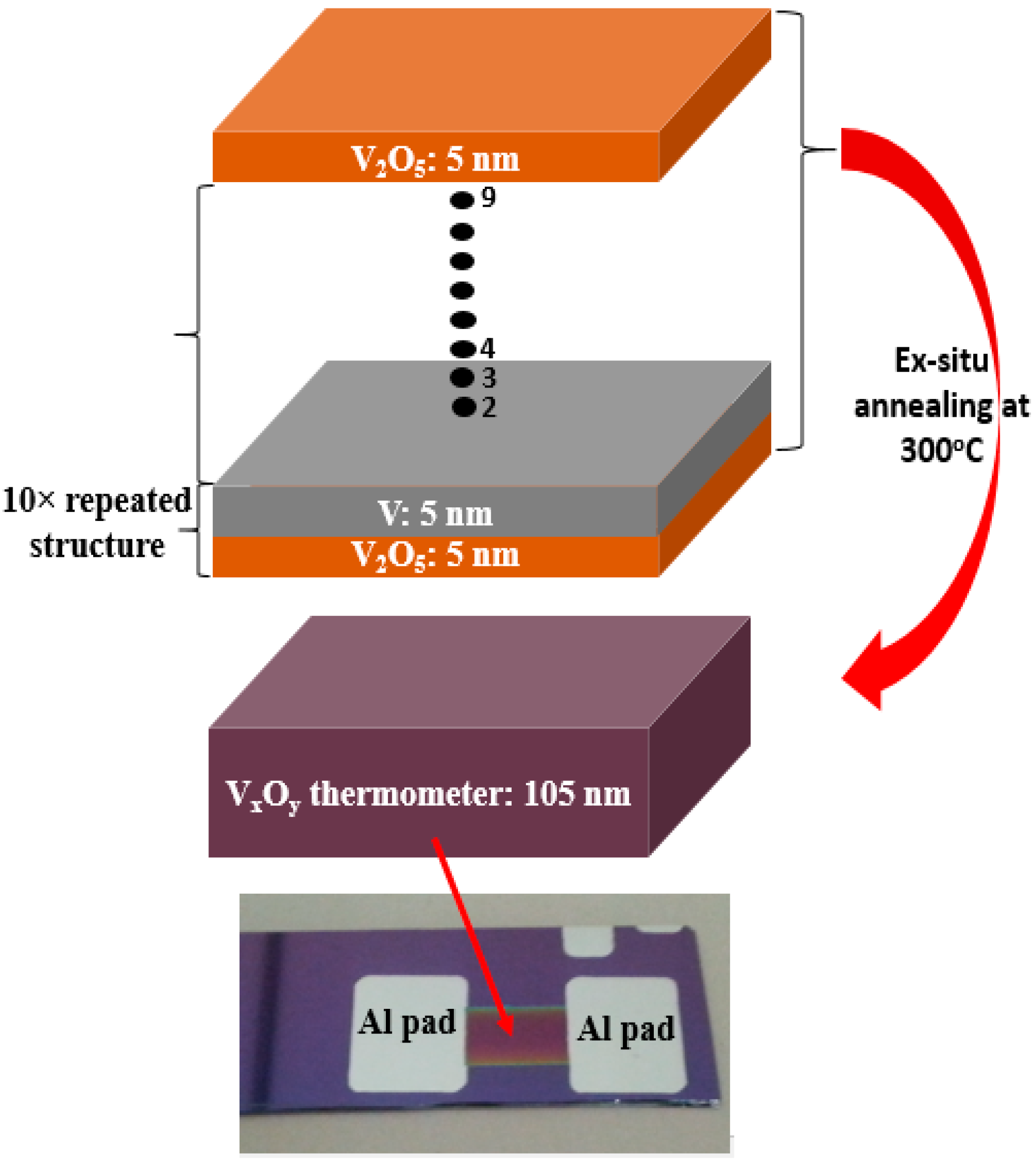
2. Materials and Methods
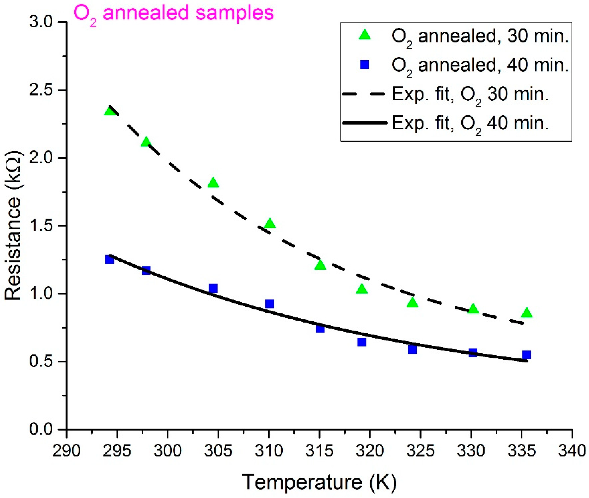
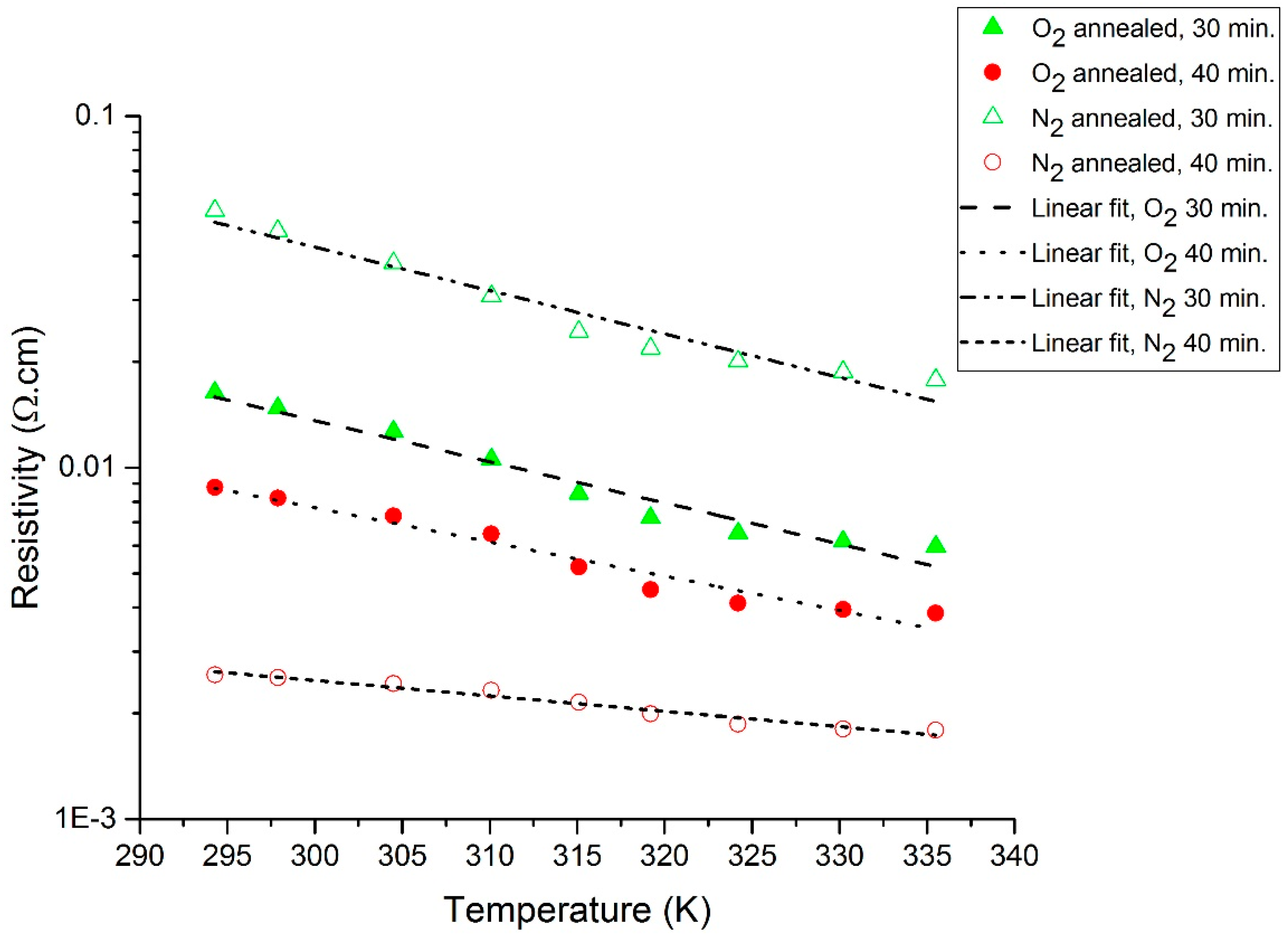
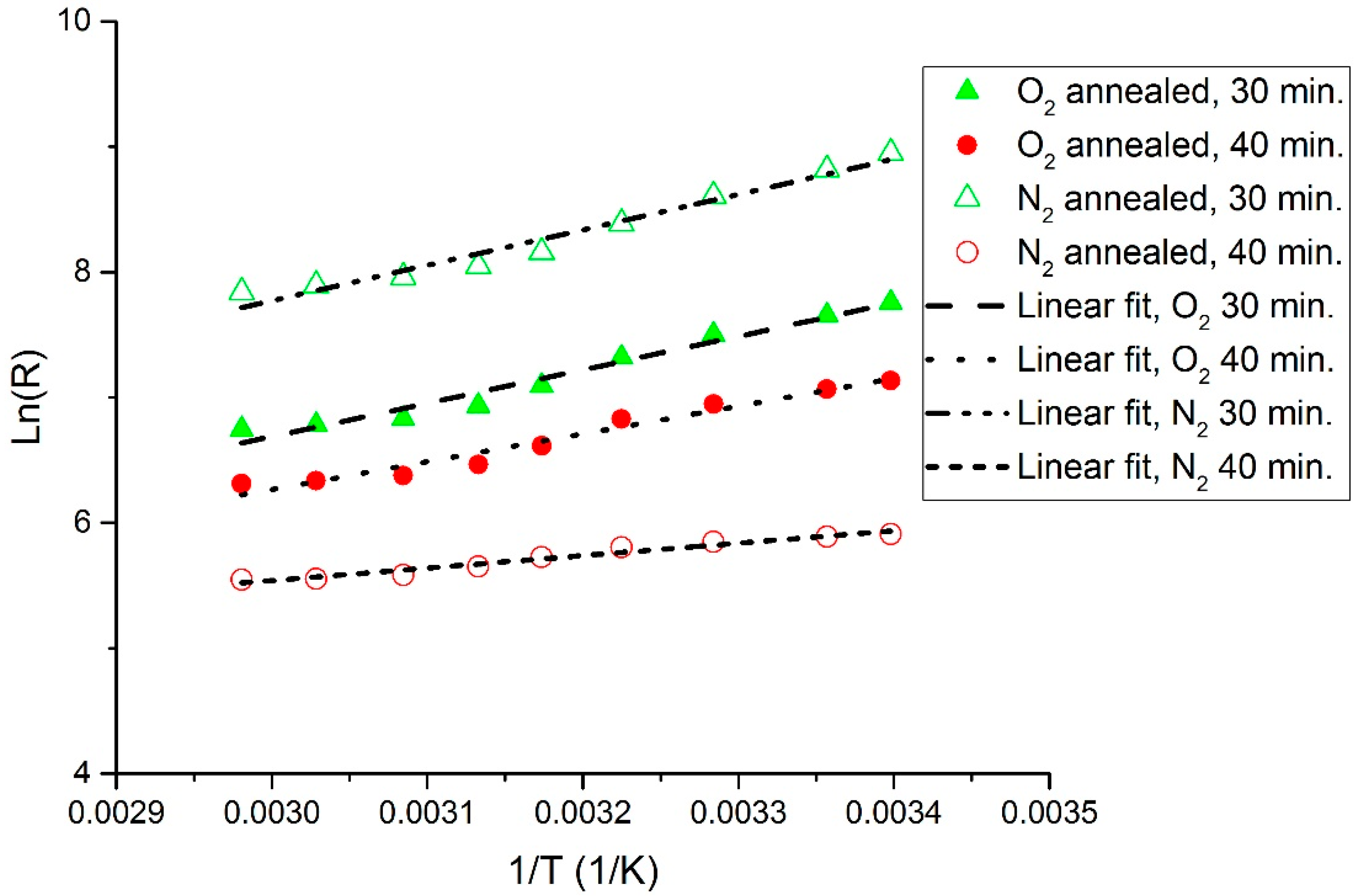
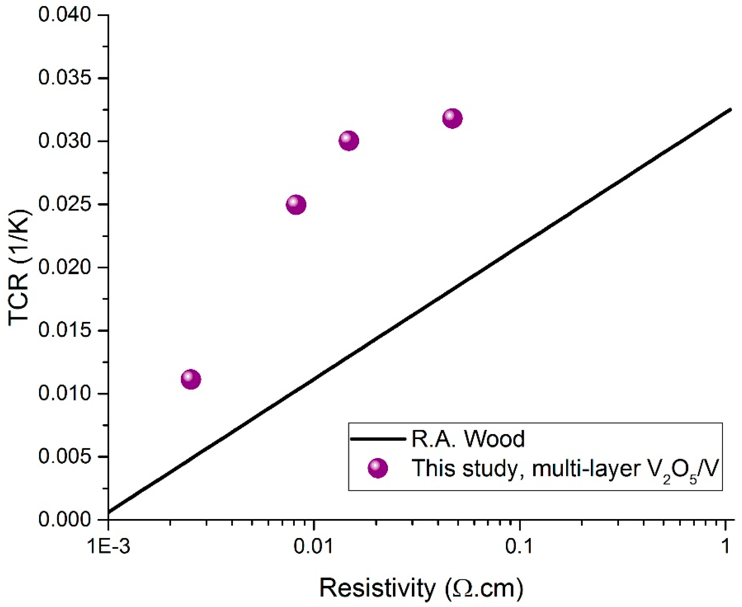
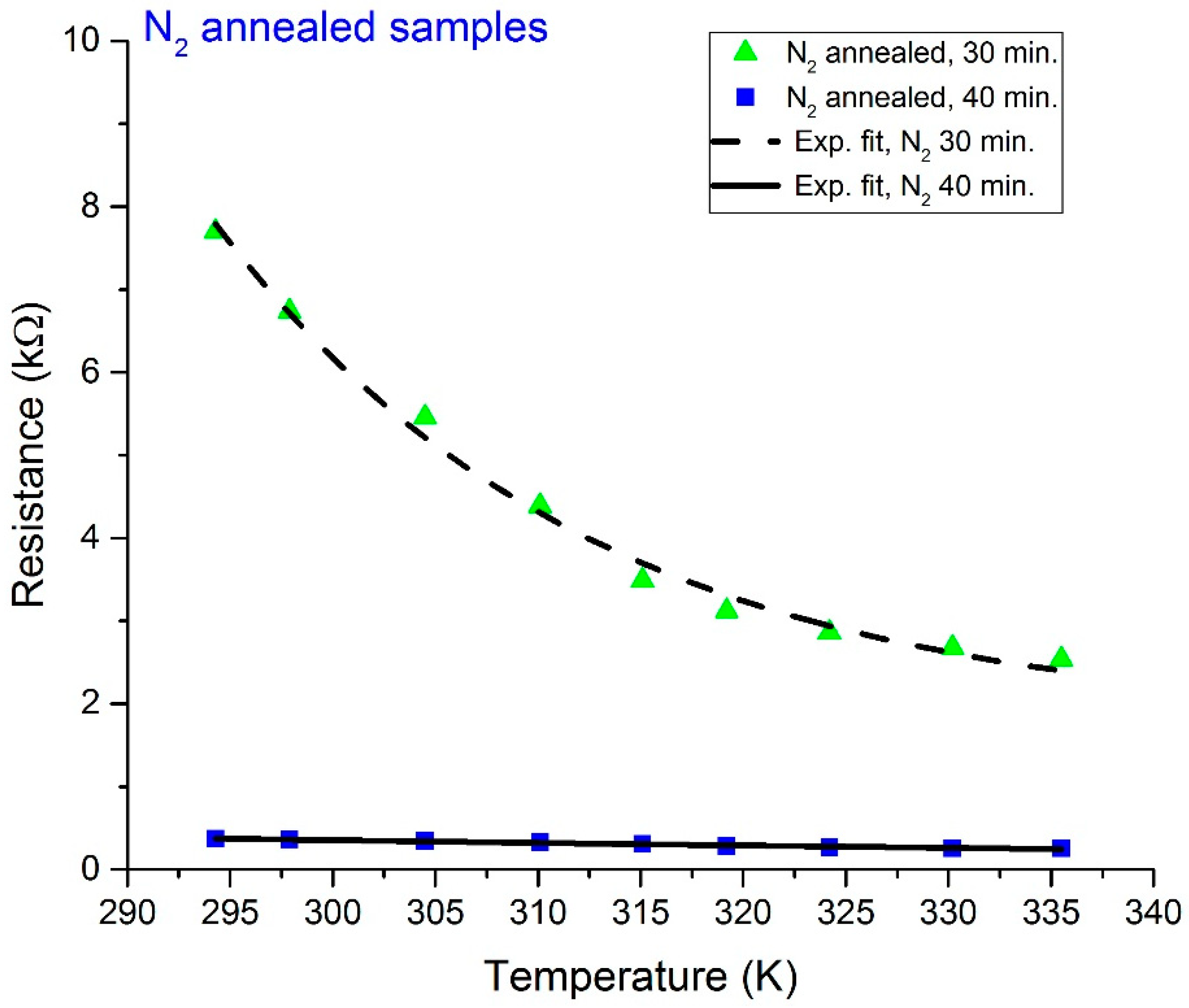
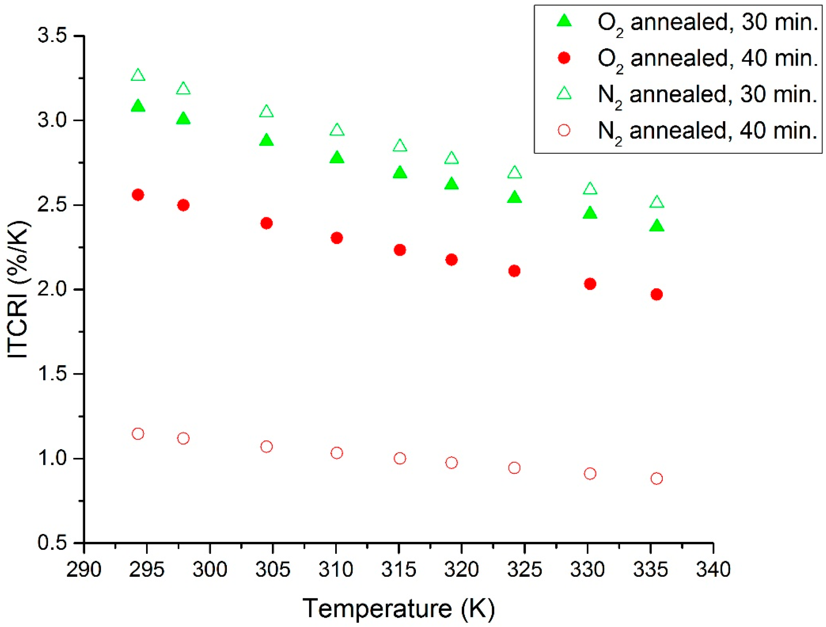
The synthesis process of the developed vanadium oxide, VxOy, thin films and a photograph of one of the fabricated resistive thermometers are shown in Figure 1. The VxOy thin films were sputter-deposited on silicon substrates having 300 nm of silicon dioxide on top of them. The VxOy thin films were synthesized via sputter coating alternating multi-layers of V2O5 and V, each having a thickness of 5 nm. The thickness of the whole sputter-deposited multi-layer structure is 105 nm. The deposited multi-layer structure was sputtered through a mechanical mask to yield a resistive thermometer with dimensions 9 mm × 6 mm. The V2O5 layers were sputter-deposited from a 99.5% pure V2O5 target at 150 W of RF power with a deposition rate of 0.75 nm/min. The V layers were sputter-deposited from a 99.9% pure V target at 150 W of DC power with a deposition rate of 4 nm/min. The sputtered multi-layered structures were then ex-situ annealed in a horizontal tube furnace at 573 K for 30 and 40 min in O2 and N2 atmospheres. Aluminum (Al) metal, having a thickness of 120 nm, was then DC sputter-deposited through a second mechanical mask to form the contact pads for the resistive thermometers. All sputter deposition operations were performed at a chamber base pressure of 2 × 10⁻⁶ Torr and at 3 mTorr of argon pressure.
For the purpose of electrical characterization, R-T measurements were performed. The measured results were then plotted and analyzed. The resistive thermometers were placed on a hot plate, which was in turn placed on the Cascade Microtech’s probe station. The hot plate’s temperature varied from 294.3 to 337 K, and the resistance of the thermometer structures was recorded in steps of approximately 5 K. For measuring the resistance, Agilent’s U1521 Multimeter was connected to the Mircotech’s microprobes, and the probes were made to contact the Al pads of the resistive thermometers.

3. Results

The measured R-T characteristic plots for the O2- and N2-annealed VxOy thermometer thin films are shown in Figure 2 and Figure 3, respectively. In addition, Figure 4 displays a re-plot of the measured R-T characteristics for the structure annealed for 40 min. in N2; this figure is presented for better scale clarity. The relationship between resistance and temperature reveals a clear semiconducting behavior, as the resistance decreases with the increase in temperature. The resistance versus temperature behavior is commensurate with the Arrhenius relationship, and the measured curves were found to be best fit using an exponential decay relationship. The resistivity versus temperature relationships are plotted in Figure 5, and Ln (R) versus 1/T Arrhenius relationships are plotted in Figure 6. The activation energies were extracted from the slopes of the fitted curves. The TCRs were calculated using Equation (2). Furthermore, the |TCR| versus temperature plots are depicted in Figure 7. A summary of all the measured and extracted parameters is given in Table 1.
The measured resistance values (at ~298 K) for the resistive thermometers annealed in O2 atmosphere were 2.11 and 1.17 kΩ for the 30 and 40 min annealed samples, respectively. This corresponds to resistivity values of 0.01477 and 0.00819 Ω·cm. The corresponding TCRs are −3.0036 and −2.4964%/K, while the measured resistance values (at ~298 K) for the resistive thermometers annealed in the N2 atmosphere were 6.74 and 0.361 kΩ for the 30 and 40 min annealed samples, respectively. This corresponds to resistivity values of 0.04718 and 0.002527 Ω·cm. The corresponding TCRs are −3.18 and −1.1181%/K. The highest observed TCR (at ~294.3 K) was −3.26%/K for the 30 min annealed sample in the N2 atmosphere. The room temperature resistivity decreased as the annealing time increased for both the O2 and N2 annealing atmospheres. This might be due to the improved intermixing between the V and V2O5 layers. Annealing for a longer period results in a vanadium-rich thin film in which the diffused vanadium atoms increase its conductivity. The improved intermixing at longer annealing times can be further verified by examining the Ro constant in Equation (1). The Ro constant is related to the conductivity prefactor, which depends on the carrier mobility and the density of states at the conduction band edge [23]. The Ro constant was extracted, and this is shown in Table 1. The Ro constant was found to increase with annealing time for both O2- and N2-annealed samples, which may indicate a reduction in carrier mobility due to an increase in carrier concentration because of improved intermixing. Moreover, it was observed that the N2-annealed thermometer thin films show much higher change in resistivity as compared to the O2-annealed films. This was expected to occur during the 30 min of annealing in O2 due to the formation of an oxide phase, which was due to the presence of O2 in the furnace. This oxide phase caused the 30 min annealed sample to possess lower resistivity. This oxide phase did not form during the 30 min of annealing in N2 due to the absence of O2 in the furnace and the incomplete diffusion of V atoms. Increasing the annealing time to 40 min increased the diffusion of V atoms, causing a phase change due to the intermixing between the V/V2O5 layers, despite the absence of O2 during the N2 annealing. Our previous analysis in [15] proved that the thin films prepared by the multilayer synthesis technique are composed of a mixture of different vanadium oxide phases. The composing vanadium oxide phases and their composition ratios can assist in explaining the above-measured behaviors.
Furthermore, the work presented in this study was compared to other research studies [13,14,15,16,17,18] involving VxOy thin films synthesized by sputter deposition of alternating multilayers of V/V2O5 or V/V2O3 followed by ex situ annealing at 300 °C in N2 or O2 atmospheres. By considering all the studies, it can be generally deduced that, increasing V content in V/V2O5 or V/V2O3 multilayer stacks reduces the resistivity of the synthesized thin film. When considering the studies concerned with the V/V2O5 multilayer stacks annealed at 300 °C in an N2 atmosphere, it can be seen that, for a V/V2O5 ratio of 5 [13], the resistivity value was found to be 3.6 Ω·cm at a TCR of −2.42%/K. For a V/V2O5 ratio of 3 [16], the resistivity value was found to be 2.68 Ω·cm at a TCR of −3.55%/K. For a V/V2O5 ratio of 1 (this work), the resistivity value was found to be 0.04718 Ω·cm at a TCR of −3.18%/K. Resistivity values are clearly decreasing with the increase in V content. Additionally, in alternating multilayers of V/V2O5, the resistivities and the TCRs of the thin films were both found to decrease as the annealing time increased from 30 to 40 min ([13], this work). Moreover, it can be generally deduced that thin films synthesized from V/V2O3 multilayer stacks [17,18] possess higher TCRs at any given resistivity value than thin films synthesized from V/V2O5 multilayer stacks [13,14,15,16]; a TCR of −3.72%/K at 0.72 Ω·cm was measured for a 30 min annealed sample in an N2 atmosphere [18].

4. Discussion

The resistive thermometer thin films developed in this work exhibit relatively high TCR values at low resistivities values. This allows for employing such thin films in different microbolometer applications. Low resistivity yields low thermal noise in addition to low power dissipation in the microbolometer. This can be useful, especially, for microbolometers employed in low power thermal imaging systems where low power consumption is sought. It is generally known that the temperature sensing layers in commercial VOx microbolometers have TCRs ranging from approximately −2 to −3%/K [1,2,4] with corresponding resistivities between 0.07 to 1.1 Ω·cm [1,2]. The resistive thermometer layers developed in this work possessing TCRs between −2 to −3%/K have lower resistivities, between 0.00819 and 0.04718 Ω·cm. Further, the TCR/resistivity performance of the resistive thermometers developed in this work were compared to the literature-standard results in [4], where VOx thin films were produced using ion-beam deposition. This comparison is represented graphically in Figure 8. The line plot (black) represents the results in [4] and was generated by plotting the equation: TCR = 0.03227 + 0.010556·log(x), where x is the resistivity in Ω·cm. The violet dots represent the values achieved in this paper. It is clear from the plot that the resistive thermometer thin films developed in this work possess higher TCRs at any given resistivity value. Additionally, when comparing the results achieved in this work to the results in [31,32], where VOx thin films were produced by reactive pulsed-dc magnetron sputtering with and without substrate bias, it can be seen that, in most of the cases, the work presented in this paper shows higher TCRs at any given resistivity value. Another notable result is the low resistivity, 2.527 × 10⁻³ Ω·cm, and moderate TCR, −1.1181%/K, achieved by annealing in an N2 atmosphere for 40 min. This resistivity yields thermometer resistances matchable to real antenna impedances in antenna-coupled microbolometer configurations. Here, it is worth pointing out the work in [10], where VOx thermometers were coupled with gold (Au) antennas and yielded 5× higher infrared responsivity compared to Au antennas coupled with niobium (Nb) thermometers. The authors, however, revealed neither the synthesis method nor the resistance or TCR of the fabricated VOx thermometer. Moreover, it is worth mentioning that the synthesis technique used in this work is CMOS-compatible, as the annealing temperatures do not exceed 300 °C; this makes the resistive thermometer layers suitable for monolithic integration with CMOS ROICs. Furthermore, for an estimate of the 1/f noise of microbolometers containing the thin films presented in this study, we referred to [33]. In [33], the noise of microbolometers based on VxOy thin films fabricated using the multilayer synthesis method was found to be 29.41 μV/√Hz at a modulation frequency of 100 Hz; those devices were 1/f noise-limited. Accordingly, the 1/f noise of microbolometers containing the thin films presented in this study are expected to have 1/f noise values of the same order of magnitude.

5. Conclusions

In this paper, the multi-layer synthesis technique was used to realize resistive thermometers with different TCR & resistivity values useful for both microbolometer and antenna-coupled microbolometer configurations. When compared with other results, it can be seen that the TCR values achieved in this work are higher than others at any given resistivity value. This would be useful in making microbolometers in thermal imaging systems requiring low power consumption. Remarkably, the 40 min annealed thin film yielded a resistive thermometer with low resistivity, 2.527 × 10⁻³ Ω·cm, which allows matching a microbolometer to real antenna impedances in antenna-coupled microbolometer configurations and simultaneously maintain a moderate TCR value that allows for acceptable responsivity. The achieved results in this paper are promising and therefore suggest that more studies be done. Specifically, the 1/f noise performance and the compositional nature of the synthesized VxOy thin films need to be studied.

Author Contributions

Conceptualization: M.A.-R., M.Z., and M.A.; fabrication and testing: M.Z.; analysis: M.A.-R.; writing—original draft preparation: M.A.-R.; writing—review and editing: M.A.-R. and M.A.; funding acquisition: M.A. and M.A.-R.

Funding

The authors extend their appreciation to the Deanship of Scientific Research at King Saud University for funding this work through research group No. (RG-1440-055).

Conflicts of Interest

The authors declare no conflict of interest.

References

  1. Kruse, P.W. Uncooled Thermal Imaging Arrays, Systems, and Applications; SPIE: Washington, DC, USA, 2002. [Google Scholar]
  2. Niklaus, F.; Vieider, C.; Jakobsen, H. MEMS-based uncooled infrared bolometer arrays: A review. In Proceedings of the SPIE on MEMS, MOEMS Technologies and Applications III, Beijing, China, 11–15 November 2007; SPIE: Washington, DC, USA, 2008. [Google Scholar]
  3. Dem’yanenko, M.A.; Esaev, D.G.; Ovsyuk, V.N.; Fomin, B.I.; Aseev, A.L.; Knyazev, B.A.; Kulipanov, G.N.; Vinokurov, N.A. Microbolometer detector arrays for the infrared and terahertz ranges. J. Opt. Technol. 2009, 76, 739–743. [Google Scholar] [CrossRef]
  4. Wood, R.A. Monolithic Silicon Microbolometer Arrays. In Semiconductors and Semimetals; Kruse, P.W., Skatrud, D.D., Eds.; Elsevier: Amsterdam, The Netherlands, 1997. [Google Scholar]
  5. Mubarak, M.H.; Sidek, O.; Abdel-Rahman, M.R.; Mustaffa, M.T.; Mustapa Kamal, A.S.; Mukras, S.M. Nano-Antenna Coupled Infrared Detector Design. Sensors 2018, 18, 3714. [Google Scholar] [CrossRef] [PubMed]
  6. Gonzalez, F.; Ilic, B.; Alda, J.; Boreman, G. Antenna-coupled infrared detectors for imaging applications. IEEE J. Sel. Top. Q. 2005, 11, 117–120. [Google Scholar] [CrossRef]
  7. Middlebrook, C.T.; Krenz, P.M.; Lail, B.A.; Boreman, G.D. Infrared phased-array antenna. Microw. Opt. Technol. Lett. 2008, 50, 719–723. [Google Scholar] [CrossRef]
  8. Krenz, P.; Alda, J.; Boreman, G.D. Orthogonal infrared dipole antenna. Infrared Phys. Technol. 2008, 51, 340–343. [Google Scholar] [CrossRef]
  9. González, F.J.; Boreman, G.D. Comparison of dipole, bowtie, spiral and log-periodic IR antennas. Infrared Phys. Technol. 2005, 46, 418–428. [Google Scholar] [CrossRef]
  10. Gonzalez, F.J.; Abdel-Rahman, M.A.; Boreman, G.D. Antenna-coupled VOx thin film microbolometer array. Microw. Opt. Technol. Lett. 2003, 38, 235–237. [Google Scholar] [CrossRef]
  11. Miller, A.J.; Luukanen, A.; Grossman, E.N. Micromachined antenna-coupled uncooled bolometers for terahertz imaging. In Proceedings of the SPIE 5411, Terahertz for Military and Security Applications II, Orlando, FL, USA, 12–16 April 2004; SPIE: Washington, DC, USA, 2004. [Google Scholar]
  12. Nolen, S.; Koch, J.A.; Paulter, N.G.; Reintsema, C.D.; Grossman, E.N. Antenna-coupled niobium bolometers for mm-wave imaging arrays. In Proceedings of the SPIE Conference on Terahertz and Gigahertz Photonics, Denver, CO, USA, 18–23 July 1999; SPIE: Washington, DC, USA, 1999. [Google Scholar]
  13. Abdel-Rahman, M.; Ilahi, S.; Zia, M.F.; Alduraibi, M.; Debbar, N.; Yacoubi, N.; Ilahi, B. Temperature coefficient of resistance and thermal conductivity of vanadium oxide ‘Big Mac’ sandwich structure. Infrared Phys. Technol. 2015, 71, 127–130. [Google Scholar] [CrossRef]
  14. Zia, M.; Abdel-Rahman, M.; Alduraibi, M.; Ilahi, B.; Alasaad, A. Synthesis and electrical characterization of vanadium oxide thin film thermometer for microbolometer applications. Electron. Lett. 2016, 52, 827–828. [Google Scholar] [CrossRef]
  15. Ilahi, B.; Abdel-Rahman, M.; Zaaboub, Z.; Zia, M.; Alduraibi, M.; Maaref, H. Thermal annealing induced multiple phase in V/V2O5 alternating multilayer structure. Int. J. Mod. Phys. B 2016, 30, 1650210. [Google Scholar] [CrossRef]
  16. Zia, M.; Abdel-Rahman, M.; Alduraibi, M.; Ilahi, B.; Awad, E.; Majzoub, S. Electrical and infrared optical properties of vanadium oxide semiconducting thin film thermometers. J. Electron. Mater. 2017, 46, 5978–5985. [Google Scholar] [CrossRef]
  17. Abdel-Rahman, M. Vanadium Oxide Thin Films with High Midwave & Longwave Infrared Thermo-Optic Coefficients and High Temperature Coefficients of Resistance. Optik 2018, 159, 79–86. [Google Scholar]
  18. Abdel-Rahman, M.; Alduraibi, M.; Zia, M.; Bahidra, E.; Alasaad, A. Vanadium sesquioxide (V2O3)-based semiconducting temperature sensitive resistors for uncooled microbolometers. Mod. Phys. Lett. B 2017, 31, 1750145. [Google Scholar] [CrossRef]
  19. Généreux, F.; Provençal, B.; Tremblay, M.; Boucher Julien, C.; Alain, C. Vanadium oxide thin film with improved sheet resistance uniformity. In Proceedings of the SPIE on Infrared Technology and Applications XL, Baltimore, MD, USA, 5–9 May 2014; SPIE: Washington, DC, USA, 2014. [Google Scholar]
  20. Benirschke, D.; Howard, S. Characterization of a low-cost, commercially available, vanadium oxide microbolometer array for spectroscopic imaging. Opt. Eng. 2017, 56, 040502. [Google Scholar] [CrossRef]
  21. Fisette, B.; Tremblay, M.; Oulachgar, H.; Généreux, F.; Béland, D.; Beaupré, P.; Julien, C.; Gay, D.; Deshaies, S.; Terroux, M.; et al. Novel vacuum packaged 384 × 288 broadband bolometer FPA with enhanced absorption in the 3–14 µm wavelength range. In Proceedings of the SPIE 10177, Infrared Technology and Applications XLIII, Anaheim, CA, USA, 9–13 April 2017; SPIE: Washington, DC, USA, 2017. [Google Scholar]
  22. Frame, J.D.; Green, N.G.; Kubo, W.; Fang, X. Plasmonic vanadium dioxide microbolometers with wavelength and polarisation sensitivity. In Proceedings of the SPIE 10722, Plasmonics: Design, Materials, Fabrication, Characterization, and Applications XVI, San Diego, CA, USA, 19–23 August 2018; SPIE: Washington, DC, USA, 2018. [Google Scholar]
  23. Ajmera, S.K.; Syllaios, A.J.; Tyber, G.S.; Taylor, M.F.; Hollingsworth, R.E. Amorphous silicon thin-films for uncooled infrared microbolometer sensors. In Proceedings of the SPIE 7660 on Infrared Technology and Applications XXXVI, Anaheim, CA, USA, 5–9 April 2010; SPIE: Washington, DC, USA, 2010. [Google Scholar]
  24. Tissot, J.-L.; Mottin, E.; Martin, J.-L.; Yon, J.-J.; Vilain, M. Advanced uncooled infrared focal plane development at CEA/LETI. In Proceedings of the SPIE 10569, International Conference on Space Optics—ICSO 2000, Toulouse Labège, France, 5–7 December 2000; SPIE: Washington, DC, USA, 2017. [Google Scholar]
  25. Shin, C.; Pham, D.P.; Park, J.; Kim, S.; Lee, Y.-J.; Yi, J. Structure and electrical properties of boron doped hydrogenated mixed-phase silicon films for uncooled microbolometer. Infrared Phys. Technol. 2019, 96, 84–88. [Google Scholar] [CrossRef]
  26. Voshell, A.; Dhar, N.; Rana, M.M. Materials for microbolometers: Vanadium oxide or silicon derivatives. In Proceedings of the SPIE 10209, Image Sensing Technologies: Materials, Devices, Systems, and Applications IV, Anaheim, CA, USA, 9–13 April 2017; SPIE: Washington, DC, USA, 2017. [Google Scholar]
  27. Tilkioglu, B.T.; Bolat, S.; Tanrikulu, M.Y.; Okyay, A.K. Digitally alloyed ZnO and TiO2 thin film thermistors by atomic layer deposition for uncooled microbolometer applications. J. Vac. Sci. Technol. A 2017, 35, 021513. [Google Scholar] [CrossRef]
  28. Jagtap, V.S.; Dégardin, A.F.; Kreisler, A.J. Low temperature amorphous growth of semiconducting Y-Ba-Cu-O oxide thin films in view of infrared bolometric detection. Thin Solid Films 2012, 520, 4754–4757. [Google Scholar] [CrossRef]
  29. Jeong, Y.J.; Kang, S.G.; Kwon, M.H.; Jung, H. Development of titanium oxide based 12 µm pixel pitch uncooled infrared detector. In Proceedings of the SPIE 10624, Infrared Technology and Applications XLIV, Orlando, FL, USA, 15–19 April 2018; SPIE: Washington, DC, USA, 2018. [Google Scholar]
  30. Wu, Z.-Y.; Tang, S.-F.; Zeng, H.-Y.; Lin, W.-J.; Chen, T.-C.; Gau, Y.-T. Infrared response of vanadium oxide (VOx)/SiNx/reduced graphene oxide (rGO) composite microbolometer. Microelectron. Reliab. 2018, 91, 313–318. [Google Scholar] [CrossRef]
  31. Basantani, H.A. Effect of RF Substrate Bias on Vanadium Oxide Thin Films during Reactive Pulsed DC Magnetron Sputter Deposition. Master’s Thesis, Pennsylvania State University, State College, PA, USA, 2011. [Google Scholar]
  32. Jin, Y. Reactive Sputter Deposition of Vanadium, Nickel, and Molybdenum Oxide Thin Films for Use in Uncooled Infrared Imaging. Ph.D. Thesis, Pennsylvania State University, State College, PA, USA, 2014. [Google Scholar]
  33. Abdel-Rahman, M.; Al-Khalli, N.; Zia, M.F.; Alduraibi, M.; Ilahi, B.; Awad, E.; Debbar, N. Fabrication and design of vanadium oxide microbolometer. In Proceedings of the 6th International Advances in Applied Physics and Materials Science Congress & Exhibition, Istanbul, Turkey, 1–3 June 2016; AIP: Washington, DC, USA, 2017. [Google Scholar]
Figure 1. A schematic diagram of the synthesis process of the VxOy thin films. A photograph of the fabricated resistive thermometer (bottom).
Sensors 19 01320 g001
Figure 2. Measured resistance versus temperature for O2-annealed resistive thermometers.
Sensors 19 01320 g002
Figure 3. Measured resistance versus temperature for N2-annealed resistive thermometers.
Sensors 19 01320 g003
Figure 4. Measured resistance versus temperature for the resistive thermometers annealed in N2 for 40 min.
Sensors 19 01320 g004
Figure 5. Resistivity (log scale) versus temperature plot for O2- and N2-annealed resistive thermometers.
Sensors 19 01320 g005
Figure 6. Ln(R) versus 1/T Arrhenius plot for O2- and N2-annealed resistive thermometers.
Sensors 19 01320 g006
Figure 7. |TCR| versus temperature plot for O2- and N2-annealed resistive thermometers.
Sensors 19 01320 g007
Figure 8. TCR versus resistivity for thermometer thin films developed in this work in comparison to the results published in [4].
Sensors 19 01320 g008
Table 1. Summary of measured and extracted electrical properties for V/V2O5 thin film resistive thermometers.
Sample IDResistance (kΩ) at R.T.Resistivity (Ω·cm) at R.T.TCR (%/K)ΔE (eV)Ro (Ω)
O2_30min.anneal2.110.01477−3.00360.2290.162
O2_40min.anneal1.170.00819−2.49640.19141.797
N2_30min.anneal6.740.04718−3.180.2430.517
N2_40min.anneal0.3610.002527−1.11810.08512.896

