A VCII-Based Stray Insensitive Analog Interface for Differential Capacitance Sensors


Department of Industrial and Information Engineering and Economics, University of L’Aquila, 67100 L’Aquila, Italy
*
Author to whom correspondence should be addressed.
Sensors 2019, 19(16), 3545; https://doi.org/10.3390/s19163545
Submission received: 10 July 2019
/
Revised: 4 August 2019
/
Accepted: 12 August 2019
/
Published: 14 August 2019
(This article belongs to the Special Issue Electronic Interfaces for Sensors)
Abstract
:In this paper, a novel approach to implement a stray insensitive CMOS interface for differential capacitive sensors is presented. The proposed circuit employs, for the first time, second-generation voltage conveyors (VCIIs) and produces an output voltage proportional to differential capacitor changes. Using VCIIs as active devices inherently allows the circuit to process the signal in the current domain, and hence, to benefit from its intrinsic advantages, such as high speed and simple implementation, while still being able to natively interface with voltage mode signal processing stages at necessity. The insensitiveness to the effects of parasitic capacitances is achieved through a simple feedback loop. In addition, the proposed circuit shows a very simple and switch-free structure (which can be used for both linear and hyperbolic sensors), improving its accuracy. The readout circuit was designed in a standard 0.35 μm CMOS technology under a supply voltage of ±1.65 V. Before the integrated circuit fabrication, to produce tangible proof of the effectiveness of the proposed architecture, a discrete version of the circuit was also prototyped using AD844 and LF411 to implement a discrete VCII. The achieved measurement results are in good agreement with theory and simulations, showing a constant sensitivity up to 412 mV/pF, a maximum linearity error of 1.9%FS, and acknowledging a good behavior with low baseline capacitive sensors (10 pF in the proposed measurements). A final table is also given to summarize the key specs of the proposed work comparing them to the available literature.
1. Introduction
In recent years, capacitive sensors have found numerous applications in measuring pressure, displacement, velocity, etc. [1,2,3,4,5,6,7,8,9,10]. Inside this category, there are the differential capacitive sensors, which exhibit robust performance against unwanted common-mode inputs and are capable of detecting low values of capacitive variations. Thanks to the recent advancements in CMOS technology like silicon micromachining, capacitive sensors can be easily implemented through this technology. Therefore, it is viable to integrate the sensor itself and the readout circuitry on a single chip, advancing towards the interesting field of smart sensors. The readout circuit of a smart sensor requires demanding specifications such as easy integration; low-voltage, low-power operation; high accuracy; and high speed. As the noise performance of the readout circuitry limits the overall precision, it must feature low input and output noise. In addition, the ever-growing need of markets for portable devices makes low power consumption an important factor. Therefore, as the performance of complete smart sensor is highly dependent on the readout circuitry, the development of an interface which can fulfil the above-mentioned requirements has become a hot research topic of our times.
A survey in literature reveals that different approaches have been adopted to design readout circuits for differential capacitors. However, most of the circuits presented so far fail to fulfil important features such as easy integration, low power consumption, and high accuracy. For example, the circuit presented in [11,12] includes several high value resistors, capacitors, and a large number of active building blocks, which results in large chip area and very high power consumption. The solutions reported in [13,14,15,16,17,18,19] employ a large number of switches and require additional controlling clock signals. Moreover, the clock feedthrough and charge injection errors of switches limit their maximum achievable accuracy. The readout circuit proposed in [8,20,21] operates on a bridge-based approach. Its main drawback is its complicated structure, which includes a differential amplifier using several matched resistors. Although adopting current mode signal processing leads to circuits with reduced complexity, high speed, and low voltage operation [7,8,10,22], when the sensor is excited by a current source, the parasitic capacitances become a limiting factor since it consumes part of the input current. As a consequence, the readout circuitry is applicable in those cases where the sensor capacitance is much larger than parasitic capacitance. For example, the interfaces presented in [7,22] are based on the current mode approach, enjoying a very simple structure, but the circuits allow less than 40% of capacitor changes and suffer from a limited accuracy. In the current mode readout circuit presented in [10], a mechanism has been adopted to compensate the effect of parasitic capacitance. However, there are three switches in the circuitry, which demands a control by additional clock signals. Moreover, the clock feedthrough and charge injection errors limit the circuit’s overall accuracy.
In this paper, we describe and prototype a novel current mode interface based, for the first time, on the second-generation voltage conveyor, a three terminal active block that, differently from Op-Amps or second-generation current conveyors (CCIIs), allows for both current domain and voltage domain signal processing without adding extra components or losing performances [23,24,25,26,27,28,29,30]. The interface fulfils many important features namely: Very simple implementation and insensitivity to large sensor parasitic capacitances thanks to an active compensation of the current taken from them. Notably, even when the parasitic capacitance has a large value in the order of the baseline, the proposed circuit exhibits high accuracy and high linearity with high read time, which are comparable to those of previously reported works, while it employs a very simple structure and avoids using any complicated switching circuitry. As an innovative solution, to charge and discharge the sensor capacitors, a square wave current signal is used to excite the sensor. Therefore, the errors and complexity related to switches are avoided. As a result, the proposed circuit features high measure accuracy and high linearity even at maximum sensor variation. To cancel the effect of parasitic capacitance, the current wasted by the parasitic capacitance is determined by a simple second-generation voltage conveyors (VCII)-based summing circuitry and an appropriate compensation current is fed back to input. Therefore, low value sensor changes are detectable by the readout circuitry. The differential capacitor variation is measured by a simple VCII-based current differencing circuit, which produces an output voltage proportional to sensor variation at a low impedance voltage output port. The circuit is completely suitable for integration as it enjoys a very simple structure employing CMOS transistors, single grounded capacitor, and two low-valued resistors. To consider the effect of nonidealities, and to confirm the effectiveness of the working principle, the circuit has been prototyped and measurement results are given. The outline of the presented work is as follows. In section two the basic theory of differential capacitor sensor is presented. In section three a general overview of the main VCII features is given, together with the detailed description of the proposed interface. In section four the simulation results of the designed readout circuit and the measurements on the prototyped circuit are given. Finally, section five concludes the paper.
2. Basic Theory
Figure 1 shows the schematic and structural diagram of a differential capacitive sensor. As it is shown, a differential capacitive sensor has three plates, two of them fixed and the middle one capable of moving. The parameter x is defined as the variation of C1 and C2 (under the action of the measurand) with respect to each capacitor value in static condition (C0/2 = Cbl), called baseline value. In the case when the overlapping area of capacitors changes under the action of a measurand (Figure 1b), there will be a linear relationship between C1–C2 and measurand x, as it is stated in Equation (1). In the case when the stimulus affects the distance between capacitors plates (Figure 1c), the relationship between C1–C2 and the measurand x becomes hyperbolic, according to Equation (2).
For both linear and hyperbolic cases, the relationship between C1–C2 and x (−1 < x < 1) is a ratiometric parameter expressed by Equation (3):
Figure 2 shows a differential capacitor (C1, C2), and its parasitic capacitance (Cp), excited by a current source. In the ideal case where there is no parasitic capacitance (Cp = 0), the value of x can be obtained by simply writing i1 − i2 as:
In the real case where Cp exists, a part of Iref (namely, ip) is taken by Cp. In this case, we can write:
Currents i1 and i2 can be written as:
where the parameters λ and (1 − λ) can be respectively written, according to the Kirchhoff current law (KCL), as:
We can therefore use the difference between the two currents flowing into the sensor to evaluate the x parameter:
As it is seen from Equation (8), the effect of the parasitic capacitance is then a loss of sensitivity of any interface that uses the difference of the two currents in order to evaluate the measurand x. This can be negligible for high baseline sensors (thousands of pF), but it drastically reduces the sensitivity of the readout circuit for small baseline sensors (tens of pF or less). In the following section, the proposed approach to cancel the effect of Cp is also presented.
3. The Proposed Interface
The proposed readout circuitry is shown in Figure 3. It utilizes VCII blocks and operates based on a capacitance variation to voltage conversion. VCII can be considered as the dual version of the well-known second-generation current conveyor (CCII). While its introduction is dated back to 2001 [23,24], it is recently gaining more attention [24,25,26]. VCII has been profitably used in fields like current-mode Wheatstone bridges [27], active filters [28], and interfaces for silicon photomultipliers [29,31]. It is characterized by a current buffer between Y and X terminals (having named β the ratio between Ix and Iy) and a voltage buffer between X and Z terminals (having named α the ratio between Vz and Vx). The Y and Z terminals are of the low impedance kind (ideally zero). The X node is a high impedance terminal (ideally infinite). The relationship between current and voltage signals of VCII is represented as:
In the ideal case α and β are in unity.
With the aim of cancelling the effect of parasitic capacitance Cp, making the readout insensitive to it, the current taken by Cp is evaluated by subtracting the sum of the currents flowing through the sensor capacitances from the reference current and then feeding it back using a current loop (Ifb). Therefore, its effect on the overall sensitivity is cancelled.
As an innovative approach, the sensor is excited by a square wave current signal. By this solution, the charging and discharging of capacitors are automatically performed without any need to use switches. There are many implementations of square wave current source such as [32], which can be easily integrated together with interface circuit. Here, in order to test the behavior of the interface alone and to eliminate sources of uncertainties, it has preliminarily been implemented by an external voltage source followed by a resistor and a current.
The proposed circuit is composed of three main sections as follows:
- The first part is a VCII-based current summing/subtracting block composed of VCII1–VCII2 and a current source equal to Iref. The sensor input is excited by a current source equal to 2Iref. The virtual ground and low impedance at Y terminal of VCII keeps the sensor second terminal to ground. In this section, according to Equation (5), the sum of I1 and I2 is produced and the result is subtracted from Iref to obtain Ifb, which, suitably integrated, generates the current taken by Cp (Iout tends to −Ip).
- The second part is the control section, which feeds Ifb to the sensor input. As it is shown in Figure 3, it is a VCII-based current-input—current-output integrator composed of the two VCII blocks, a resistor, and a grounded capacitor.
- In the third part (output section), the difference between I1 and I2 is produced and converted to a proportional voltage signal. This operation is performed by three VCII blocks (VCII3–VCII5) and resistor Rg.
The detailed operation of the proposed circuit can be analyzed as follows. At the input node (node in), considering Iout = 0 at the initial time and writing KCL, it results:
Thanks to the virtual ground at Y ports of VCIIs, using Equation (6), for I1 and I2 we have:
As the used VCIIs have a similar internal structure at Y port, I1 and I2 will be split by half. Therefore I3, I4, I7, and I8 are obtained as:
Inserting Equations (13) and (14), respectively, into Equations (11) and (12), I3 and I4 are given by:
A simple KCL analysis at node A gives:
By considering the current buffering action between Y and X nodes of VCII, we have:
Using Equation (18), and inserting Equations (15) and (16) into Equation (17), it results:
By assuming β1 = β2 = 1, from Equation (19) we have:
In fact, at node A, a current comparing action is performed. According to Equation (20), as long as the sum of I5 and I6 is not equal to Iref (i.e., I1 + I2 is not equal to 2Iref), a non-zero compensation current (Ifb) is produced. This current is fed to the input node by the controller circuit, which is a simple VCII-based current integrator as is shown in Figure 3. By assuming virtual ground at Y port of VCII, the relationship between the input and output currents of the integrator can be expressed as:
The design of the integrator (and, in general, of the feedback controller) determines the readout speed of the interface. In particular, its time constant RC must be sufficiently smaller than the half-period of the reference current Iref, ensuring that the loop reaches the steady state before the reference signal changes polarity, consequently, completing an effective measurement.
To find the output voltage, we assume that Ip is provided by the feedback circuitry. The output voltage is equal to the voltage produced at node B, which can be written as:
For I10 and I11 we have:
By assuming α4 = β3 = β4 = β5 = 1, inserting Equations (23) and (24) into Equation (22) gives the output voltage as:
As Equation (25) indicates, supposing Iref as a square wave current, the output of the interfaces is a square wave voltage, with the amplitude modulated by the sensor variations (regardless of being positive, C1 > C2, or negative C2 > C1) and the phase indicating whether C1 is greater than C2 (phase equal to 0°), or vice versa (phase equal to 180°). The gain can be easily set by Rg, therefore, the circuit enjoys a tunable sensitivity. In order to define this last parameter, it is convenient to consider ΔC as reference magnitude and, without losing generality, it is possible to write:
4. Simulation Results and Measurements
The proposed readout circuit of Figure 3 has been simulated using Spice in 0.35 μm CMOS technology and a supply voltage of ±1.65 V. For the required VCIIs, the circuit of [27] (Figure 4a) has been used with the same aspect ratios and biasing. Current sources have been implemented by means of simple current mirrors. AC and DC performances of the VCII in terms of α and β are shown respectively in Figure 4b,c. The low impedance current input (Y) is implemented by a regulated common gate (M1–M5), while the current transferring action is performed by the current mirror M6, M7. The flipped voltage follower M9, M10 allow us to obtain the voltage buffering between the X voltage input and the Z voltage output. The important parameters of the used VCIIs are summarized in Table 1.
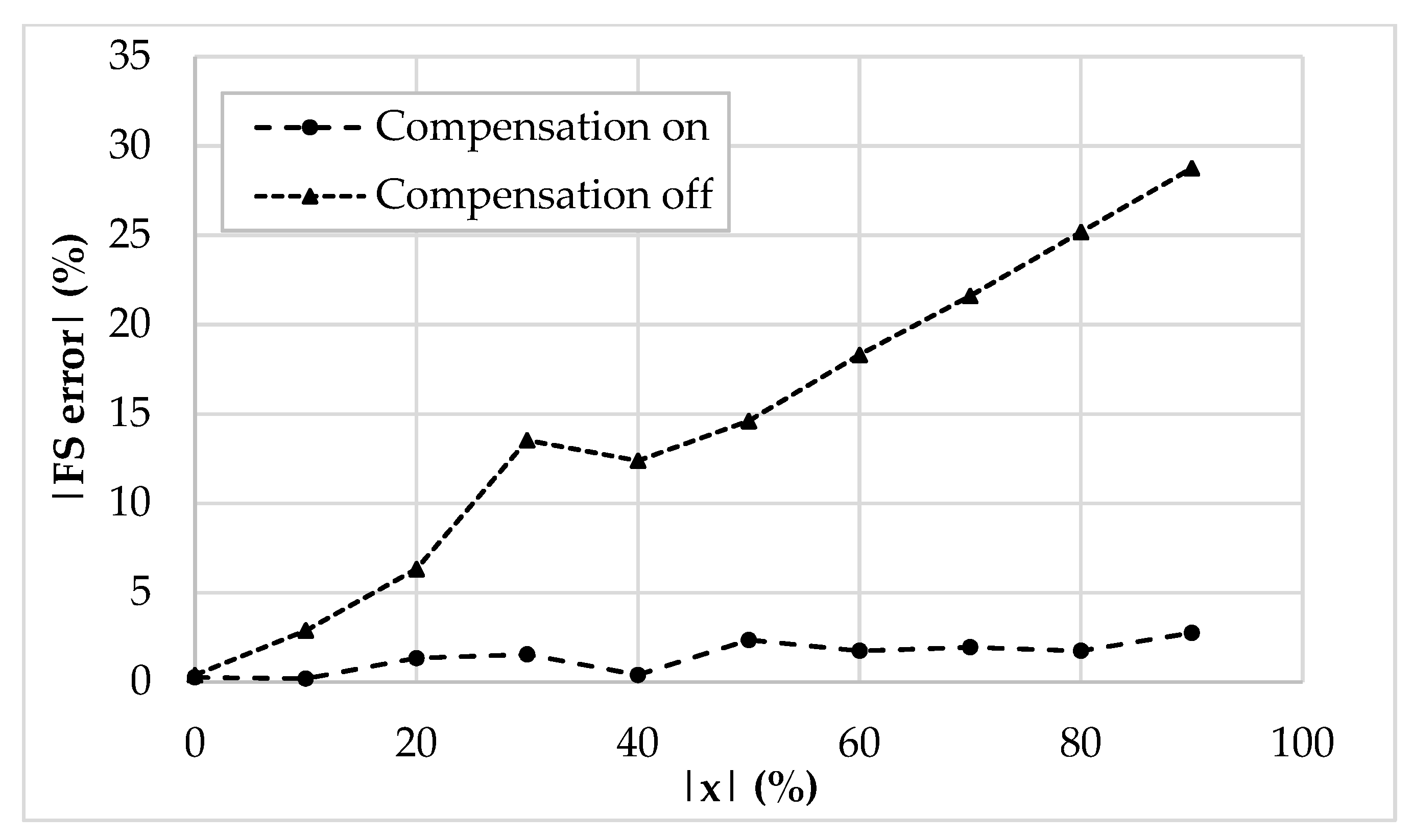
The values of Iref, Rg, R, and C have been selected as 5 μA, 12 kΩ, 1 kΩ, and 20 pF, respectively. The frequency of Iref has been chosen equal to 500 kHz to test the interface behavior close to its maximum operating condition. By setting the sensor baseline Cbl at 10 pF and the parasitic capacitance Cp at 5 pF, the simulation results where the compensation loop has been first enabled, and then disabled, are shown in Figure 5a,b, respectively. For sake of clarity, the picture shows the output voltage only in the case of phase equal to zero. As visible, without the compensation, the amplitude of the output voltage reaches only 80% of full-scale. This behavior is better shown in Figure 6, where the amplitude of each curve has been extracted and compared to ideal values. The full-scale error for each case has also been calculated and is shown in Figure 7: With compensation, the error remains below 2.1%, further proving the effectiveness of the proposed compensation technique. As it is seen, the compensation technique is very effective. It is also observed that thanks to the proposed method, the large parasitic capacitance of 5 pF does not have any effect on the output voltage. In order to analyze both the effects of VCII nonidealities and the effects of mismatches on passive and active components, a mixed simulation was carried out where a Monte Carlo analysis was performed on both PVT conditions for active devices and on tolerances for passive ones. In particular, temperature range was set from −10 °C to 80 °C, supply voltage variation from −5% to 5% of the nominal one, resistors tolerance was set to 5%, while capacitor one to 10%. The overall maximum variation from the nominal reference value was experienced at x = 90%, with a deviation from the ideality of about 3 mV. These results are achieved while the circuit consumes 5.2 mW.
To demonstrate the validity of the proposed architecture before the chip fabrication, and to obtain tangible results, a discrete version of the interface has been simulated and fabricated. The discrete VCII has been implemented as shown in Figure 8, where the current I/O of the AD844 has been used to implement a current buffer, and a simple LF411 has been suitably added to perform a voltage buffering action. Although directly available from the AD844, an external voltage buffer has been adopted in order to gain the possibility of setting an α value greater than unity. For the simulations, taking Figure 3 as reference, R and C have been again set to 1 kΩ and 20 pF, respectively, while Rg has been set to 33 kΩ.
Sensor baseline Cbl and parasitic capacitance Cp have been set to 200 pF and 120 pF, respectively. The reference current Iref has been set to 250 µA peak amplitude and 100 kHz frequency. Figure 9 acknowledges the functionality of the discrete interface and of the compensation mechanism, showing the time domain behavior (Figure 9a), the DC characteristic (Figure 9b), and the full-scale error (Figure 9c).
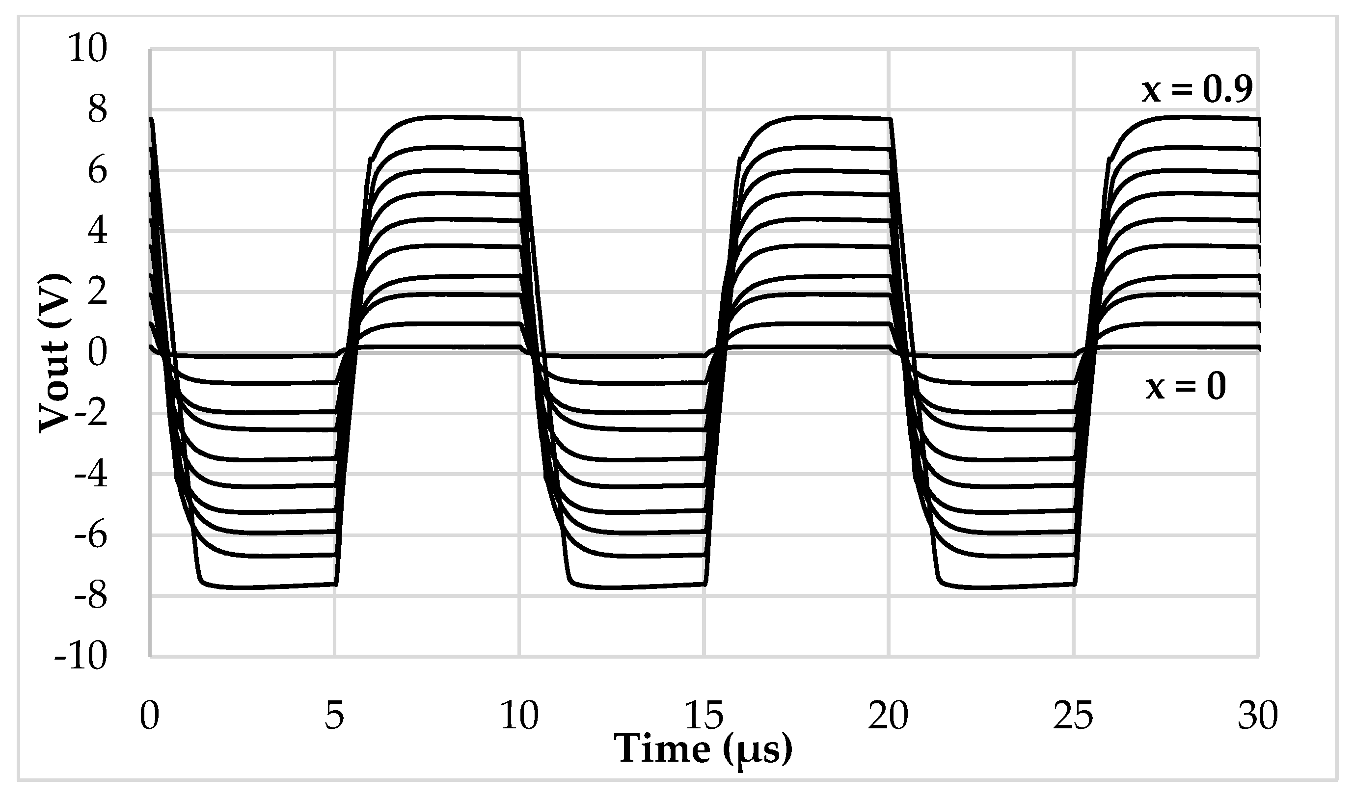
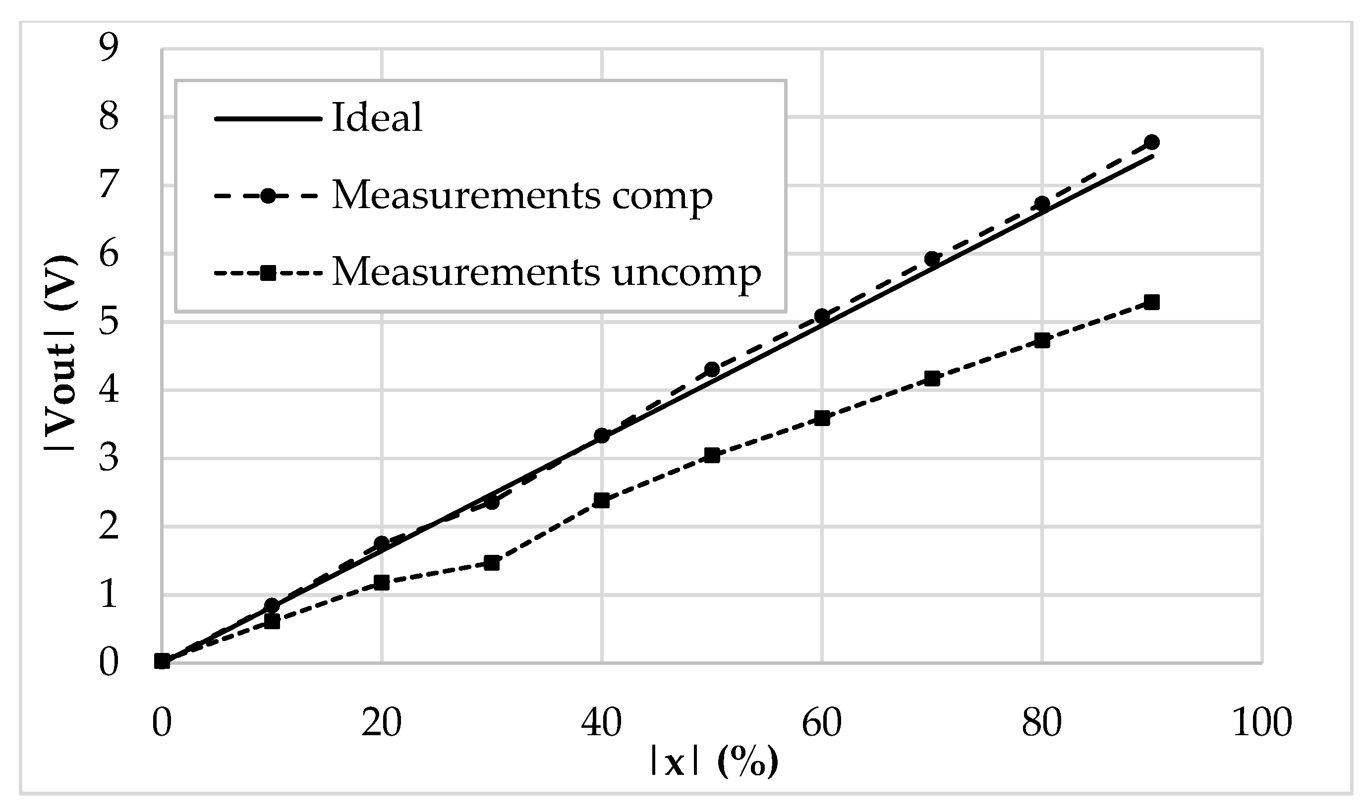
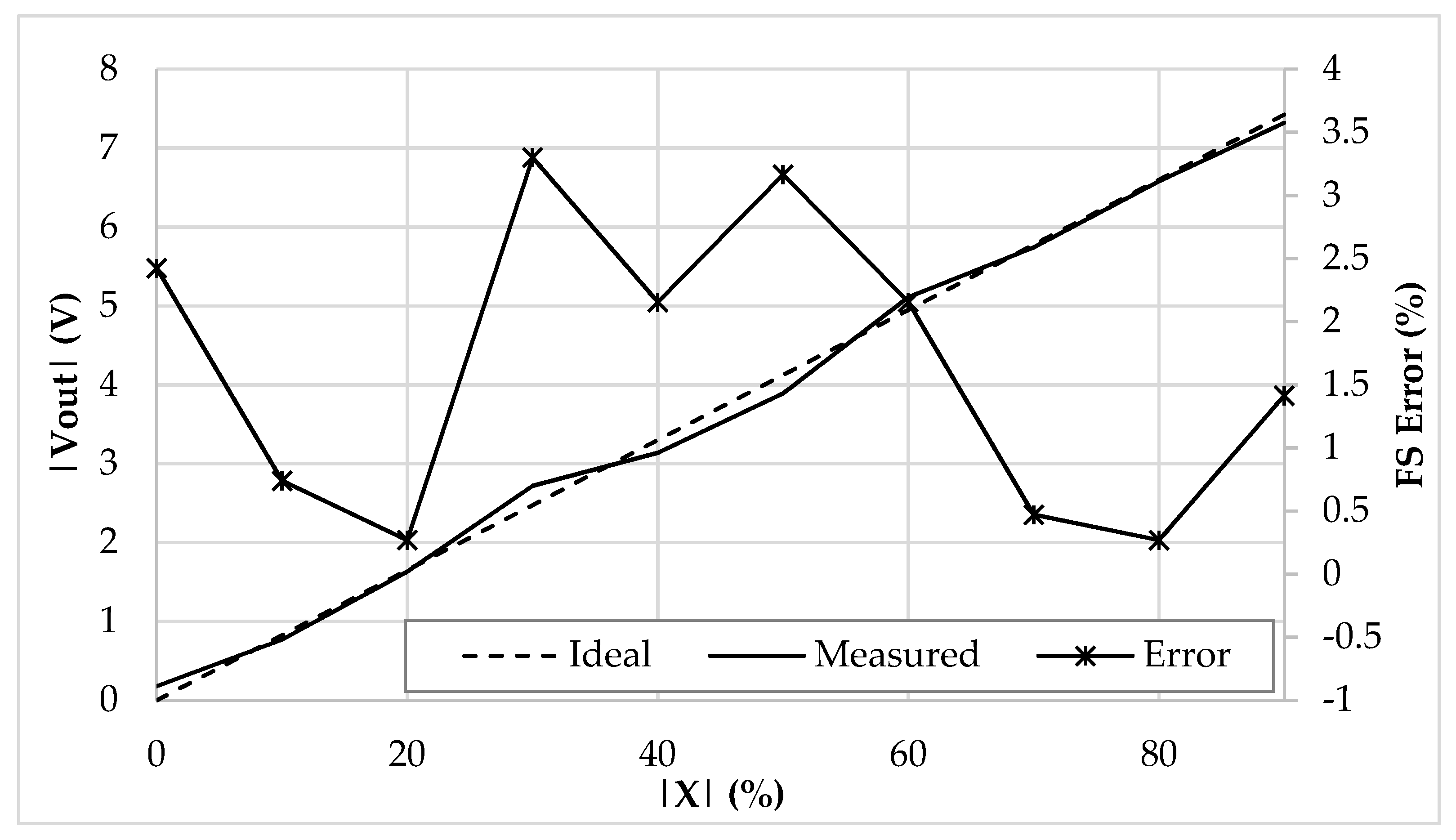
In Figure 10, the prototyped board is shown. All the parameters have been set to match the ones used in the simulation environment. The reference current has been generated through a Keysight 33600A signal generator, which, together with two resistors and two current buffers, has been able to output accurate values of 250 µA and 500 µA for Iref and 2Iref. The output voltage has been measured through a Keysight MSOX3054T oscilloscope and a Keysight N2843A probe. To emulate the behavior of a 200 pF baseline linear differential capacitive sensor (Figure 1b), a set of reference capacitors have been used. The test bench allows us to freely add parasitic capacitances as in Figure 2, so as to mimic even harsh conditions when stray capacitances are comparable to the baseline of the sensor. The time domain measurements are reported in Figure 11, while Figure 12 shows the DC characteristic of the prototype board. As visible, the behavior of the interface is very close to the simulations and the full-scale error (Figure 13) remains always below the 2.5%. The maximum linearity error is equal to 0.9%FS. The presented setup allows us to obtain a sensitivity of 21 mV/pF.
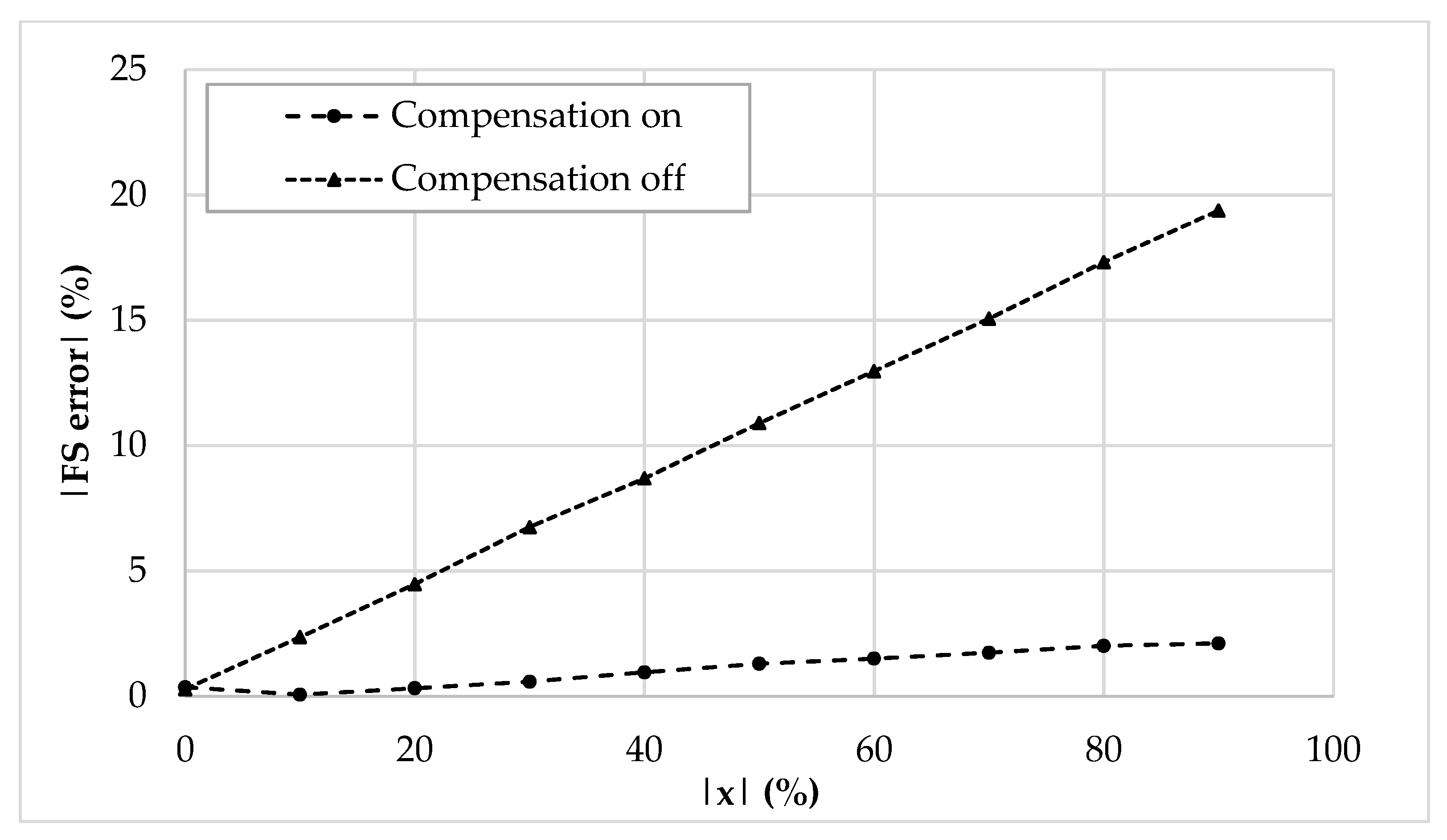
Although, without reference capacitors, the interface capability of reading very low baseline values has been investigated as well. A set of 1% tolerance capacitors was adopted to mimic a 10 pF baseline sensor. The DC characteristic is shown in Figure 14: As expected, the error increases up to the 3.3%, however, the interface still shows good behavior when the maximum linearity error is equal to 1.9%FS. The resulted sensitivity is equal to 412 mV/pF. The maximum value of C0 i.e., C0max is 200 pF, and its minimum value C0min is 10 pF. Therefore, the dynamic range is C0max − C0min = 200 pF − 10 pF = 190 pF.
Table 2 compares the presented readout technique with data available from the literature: As visible, the advantages coming from a mixed current–voltage approach, together with the consequent ease in alleviating the effects of parasitic capacitances, allow us to maintain a full-range readout capability if compared to traditional voltage mode circuits, while sensibly reducing the allowable sensors baseline. The sensitivity parameter reported in the table is calculated from the output voltage relationships of the referenced works and refers to the minimum baseline allowed by the interface. Since the circuit in [21] has a nonlinear input–output relationship, the sensitivity cannot be uniquely determined.
5. Conclusions
A parasitic insensitive readout circuit for differential capacitive sensors has been presented. The proposed circuit utilizes VCII and produces an output voltage proportional to the sensor variation. The working principle is based on the current summing and subtracting technique, resulting in a very simple yet effective implementation. To reduce the errors to the minimum value, no switches are employed. The effect of parasitic capacitances is cancelled using a very simple compensation circuit. The proposed method has been theoretically analyzed and simulated. The simulation results have shown a negligible full-scale error, even for parasitic capacitances comparable to the baseline value. The notable advantage of the proposed circuit is that the sensitivity can be simply adjusted by a resistor. Measurement collected from a discrete prototype has been given, proving good agreement with theory and simulation results and the capability of the circuit to host low baseline sensors. These results confirm the good potentiality of the proposed topology and all the benefits that could come from the on-chip measurements. Several degrees of freedom are also available for the designer to better optimize the performances to her/his necessity. A comparison with the available literature has also been proposed, highlighting the effectiveness of the presented idea and the good potential of the integrated version.
Author Contributions
Conceptualization, G.B.; Methodology, G.B; Validation, G.F. and V.S.; Formal Analysis, G.B. and L.S.; Investigation, G.B. and L.S.; Data Curation, G.F.; Writing-Original Draft Preparation, L.S.; Writing-Review & Editing, G.F. and V.S.; Supervision, G.F.; Funding Acquisition, V.S.
Funding
The work has been co-funded by the “CityMap: Sistema non invasivo per il monitoraggio delle aree di sosta (parcheggi) cittadine” project in the framework of the action “POR FESR Abruzzo 2014–2020—Linea di azione 1.1.4 - Avviso Pubblico per il Sostegno a progetti di Innovazione delle Grandi Imprese e delle PMI nelle aree di specializzazione S3”.

Conflicts of Interest
The authors declare no conflict of interest.
References
- Polak, L.; Sotner, R.; Petrzela, J.; Jerabek, J. CMOS Current Feedback Operational Amplifier-Based Relaxation Generator for Capacity to Voltage Sensor Interface. Sensors 2018, 18, 4488. [Google Scholar] [CrossRef] [PubMed]
- Brookhuis, R.; Lammerink, T.; Wiegerink, R. Differential capacitive sensing circuit for a multi-electrode capacitive force sensor. Sens. Actuators A Phys. 2015, 234, 168–179. [Google Scholar] [CrossRef]
- Royo, G.; Sánchez-Azqueta, C.; Gimeno, C.; Aldea, C.; Celma, S. Programmable Low-Power Low-Noise Capacitance to Voltage Converter for MEMS Accelerometers. Sensors 2016, 17, 67. [Google Scholar] [CrossRef] [PubMed]
- Chen, W.; Zhao, Z.; Liu, X.; Zhang, Z.; Suo, C. A Capacitive Humidity Sensor Based on Multi-Wall Carbon Nanotubes (MWCNTs). Sensors 2009, 9, 7431–7444. [Google Scholar] [CrossRef] [PubMed]
- Wang, Y.; Chodavarapu, V. Differential Wide Temperature Range CMOS Interface Circuit for Capacitive MEMS Pressure Sensors. Sensors 2015, 15, 4253–4263. [Google Scholar] [CrossRef] [Green Version]
- Hu, H.; Xu, T.; Hui, S. A high-accuracy, high-speed interface circuit for differential-capacitance transducer. Sens. Actuators A Phys. 2006, 125, 329–334. [Google Scholar] [CrossRef]
- Pennisi, S. High-performance and simple CMOS interface circuit for differential capacitive sensors. IEEE Trans. Circuits Syst. II Express Briefs 2005, 52, 327–330. [Google Scholar] [CrossRef]
- Depari, A.; Sisinni, E.; Flammini, A.; Ferri, G.; Stornelli, V.; Barile, G.; Parente, F. Autobalancing Analog Front End for Full-Range Differential Capacitive Sensing. IEEE Trans. Instrum. Meas. 2018, 67, 885–893. [Google Scholar] [CrossRef]
- Barile, G.; Ferri, G.; Parente, F.; Stornelli, V.; Depari, A.; Flammini, A.; Sisinni, E. A standard CMOS bridge-based analog interface for differential capacitive sensors. In Proceedings of the 13th Conference on Ph.D. Research in Microelectronics and Electronics (PRIME), Giardini Naxos, Italy, 12–15 June 2017. [Google Scholar]
- Scotti, G.; Pennisi, S.; Monsurrò, P.; Trifiletti, A. 88-uA 1-MHz Stray-Insensitive CMOS Current-Mode Interface IC for Differential Capacitive Sensors. IEEE Trans. Circuits Syst. I Regul. Pap. 2014, 61, 1905–1916. [Google Scholar] [CrossRef]
- George, B.; Madhu Mohan, N.; Jagadeesh Kumar, V. A Linear Variable Differential Capacitive Transducer for Sensing Planar Angles. IEEE Trans. Instrum. Meas. 2008, 57, 736–742. [Google Scholar] [CrossRef]
- Mochizuki, K.; Watanabe, K.; Masuda, T. A high-accuracy high-speed signal processing circuit of differential-capacitance transducers. IEEE Trans. Instrum. Meas. 1998, 47, 1244–1247. [Google Scholar] [CrossRef] [Green Version]
- Dimitropoulos, P.; Karampatzakis, D.; Panagopoulos, G.; Stamoulis, G. A low-power/low-noise readout circuit for integrated capacitive sensors. IEEE Sens. J. 2006, 6, 755–769. [Google Scholar] [CrossRef]
- Shiah, J.; Rashtian, H.; Mirabbasi, S. A low-noise high-sensitivity readout circuit for MEMS capacitive sensors. In Proceedings of the IEEE International Symposium on Circuits and Systems, Paris, France, 30 May–2 June 2010. [Google Scholar]
- Bracke, W.; Merken, P.; Puers, R.; Van Hoof, C. Ultra-Low-Power Interface Chip for Autonomous Capacitive Sensor Systems. IEEE Trans. Circuits Syst. I Regul. Pap. 2007, 54, 130–140. [Google Scholar] [CrossRef]
- George, B.; Kumar, V. Switched Capacitor Signal Conditioning for Differential Capacitive Sensors. IEEE Trans. Instrum. Meas. 2007, 56, 913–917. [Google Scholar] [CrossRef]
- Mohan, N.M.; Shet, A.R.; Kedarnath, S.; Kumar, V.J. Digital converter for differential capacitive sensors. IEEE Trans. Instrum. Meas. 2008, 57, 2576–2581. [Google Scholar] [CrossRef]
- Barile, G.; Ferri, G.; Parente, F.; Stornelli, V.; Sisinni, E.; Depari, A.; Flammini, A. A CMOS full-range linear integrated interface for differential capacitive sensor readout. Sens. Actuators A Phys. 2018, 281, 130–140. [Google Scholar] [CrossRef]
- Kim, H.; Lee, B.; Mun, Y.; Kim, J.; Han, K.; Roh, Y.; Song, D.; Huh, S.; Ko, H. Reconfigurable Sensor Analog Front-End Using Low-Noise Chopper-Stabilized Delta-Sigma Capacitance-to-Digital Converter. Micromachines 2018, 9, 347. [Google Scholar] [CrossRef]
- Ferri, G.; Parente, F.; Stornelli, V.; Barile, G.; Pantoli, L. Automatic Bridge-based Interface for Differential Capacitive Full Sensing. Procedia Eng. 2016, 168, 1585–1588. [Google Scholar] [CrossRef]
- Ferri, G.; Stornelli, V.; Parente, F.; Barile, G. Full range analog Wheatstone bridge-based automatic circuit for differential capacitance sensor evaluation. Int. J. Circuit Theory Appl. 2016, 45, 2149–2156. [Google Scholar] [CrossRef]
- Ferri, G.; Parente, F.; Stornelli, V. Current conveyor-based differential capacitance analog interface for displacement sensing application. AEU Int. J. Electron. Commun. 2017, 81, 83–91. [Google Scholar] [CrossRef]
- Filanovsky, I.M. Current Conveyor, Voltage Conveyor, Gyrator. In Proceedings of the 44th IEEE 2001 Midwest Symposium on Circuits and Systems, Dayton, OH, USA, 14–17 August 2001; Volume 1, pp. 314–317. [Google Scholar]
- Cajka, J.; Vrba, K. The Voltage Conveyor May Have in Fact Found its Way into Circuit Theory. Int. J. Electron. Commun. 2004, 58, 244–248. [Google Scholar] [CrossRef]
- Safari, L.; Barile, G.; Stornelli, V.; Ferri, G. An Overview on the Second Generation Voltage Conveyor: Features, Design and Applications. IEEE Trans. Circuits Syst. II Express Briefs 2019, 66, 547–551. [Google Scholar] [CrossRef]
- Barile, G.; Ferri, G.; Safari, L.; Stornelli, V. A New High Drive Class-AB FVF Based Second Generation Voltage Conveyor. IEEE Trans. Circuits Syst. II Express Briefs 2019. [Google Scholar] [CrossRef]
- Safari, L.; Barile, G.; Stornelli, V.; Ferri, G.; Leoni, A. New Current Mode Wheatstone Bridge Topologies with Intrinsic Linearity. In Proceedings of the 2018 14th Conference on Ph.D. Research in Microelectronics and Electronics (PRIME), Prague, Czech Republic, 2–5 July 2018. [Google Scholar]
- Safari, L.; Barile, G.; Ferri, G.; Stornelli, V. High performance voltage output filter realizations using second generation voltage conveyor. Int. J. Rf Microw. Comput. Aided Eng. 2018, 28, e21534. [Google Scholar] [CrossRef]
- Barile, G.; Leoni, A.; Pantoli, L.; Safari, L.; Stornelli, V. A New VCII Based Low-Power Low-Voltage Front-end for Silicon Photomultipliers. In Proceedings of the 2018 3rd International Conference on Smart and Sustainable Technologies (SpliTech), Split, Croatia, 26–29 June 2018. [Google Scholar]
- A New VCII Based Low-Power Low-Voltage Front-End for Silicon Photomultipliers. Available online: http://ieeexplore.ieee.org/stamp/stamp.jsp?tp=&arnumber=8448384&isnumber=8448303 (accessed on 13 August 2019).
- Pantoli, L.; Barile, G.; Leoni, A.; Muttillo, M.; Stornelli, V. A Novel Electronic Interface for Micromachined Si-Based Photomultipliers. Micromachines 2018, 9, 507. [Google Scholar] [CrossRef]
- Kaewpoonsuk, A.; Riewruja, V.; Rerkratn, A.; Kamsri, T. An accurate CCII-based voltage controlled current source. In Proceedings of the International Conference on Control, Automation and Systems (ICCAS), Seoul, Korea, 14–17 October 2008. [Google Scholar]
Figure 1.
Differential capacitive sensor (a) schematic and structure when the measurand influences (b) the overlapping area of plates; (c) the distance between plates.
Figure 1.
Differential capacitive sensor (a) schematic and structure when the measurand influences (b) the overlapping area of plates; (c) the distance between plates.

Figure 2.
Differential capacitive sensor excited by a current source, where parasitic capacitance Cp is evidenced.
Figure 2.
Differential capacitive sensor excited by a current source, where parasitic capacitance Cp is evidenced.
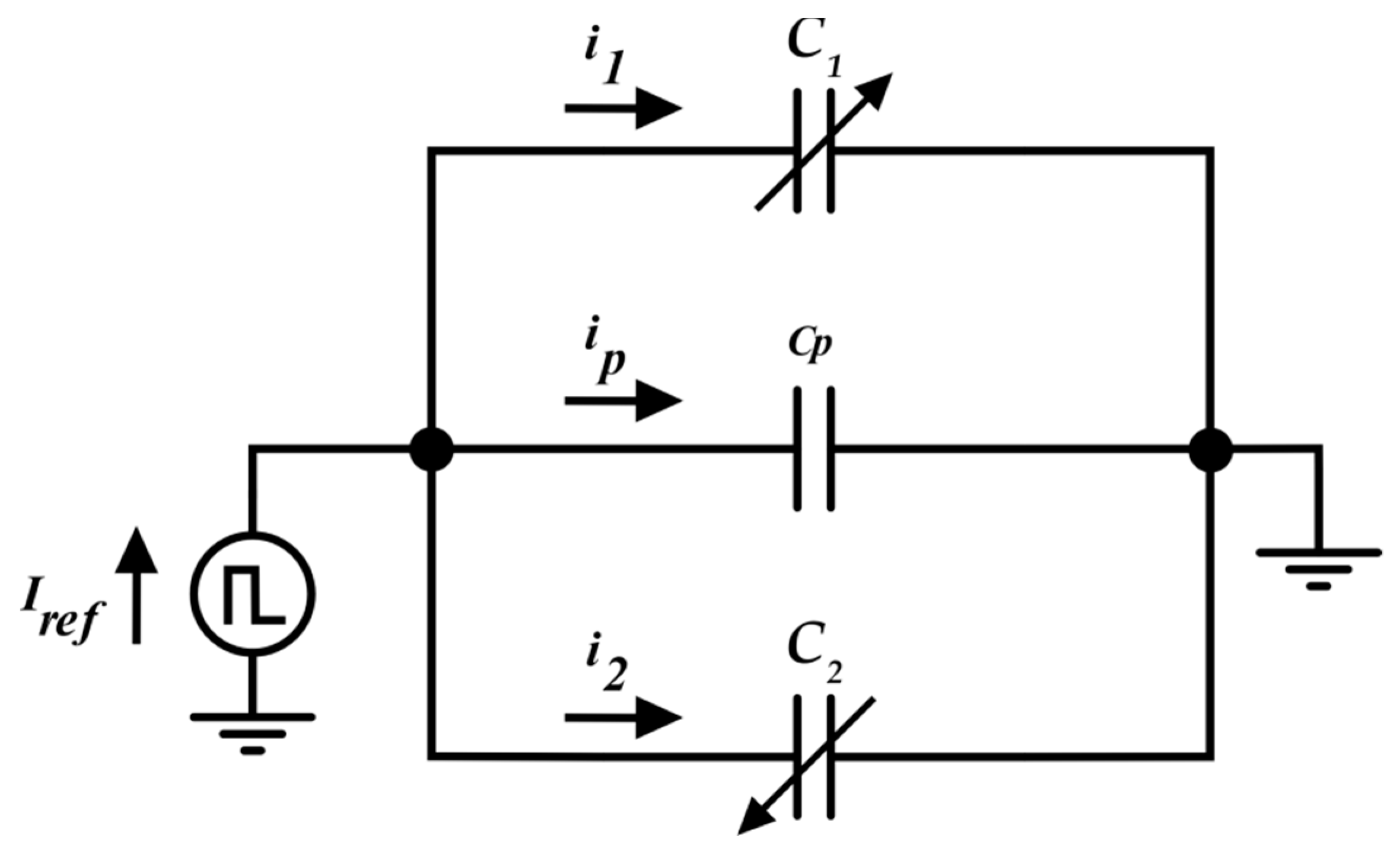
Figure 3.
The proposed second-generation voltage conveyors VCII based interface.
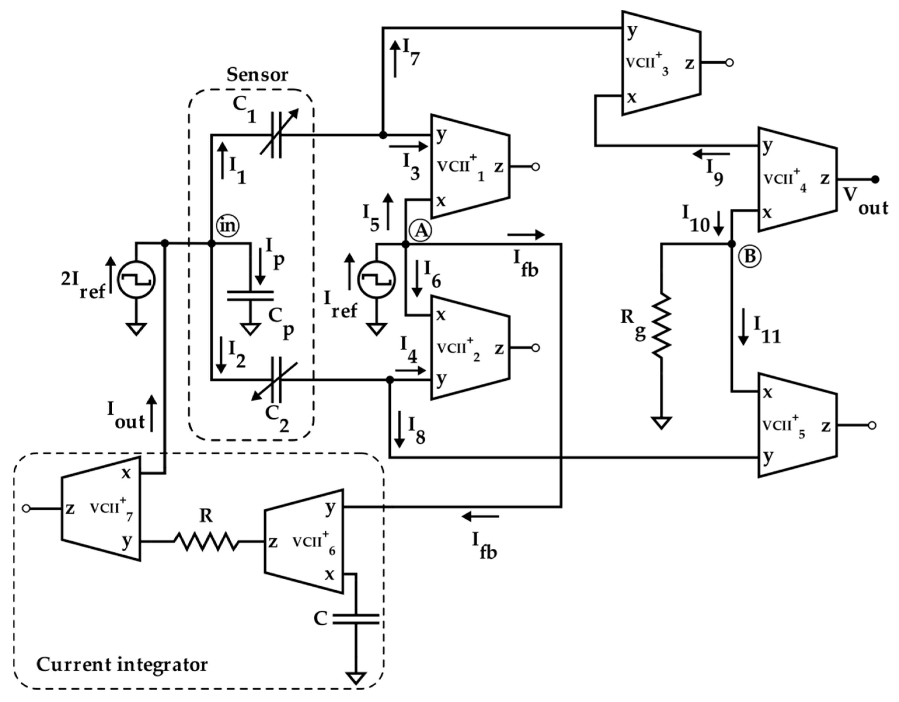
Figure 4.
The VCII used in the simulations: (a) Topology (see [27]), (b) AC performances (determined with a 3 pF load at X), (c) DC performances (determined with a 1 kΩ load at Y for β simulations, and with a 100 kΩ load at Z for α simulations).
Figure 4.
The VCII used in the simulations: (a) Topology (see [27]), (b) AC performances (determined with a 3 pF load at X), (c) DC performances (determined with a 1 kΩ load at Y for β simulations, and with a 100 kΩ load at Z for α simulations).

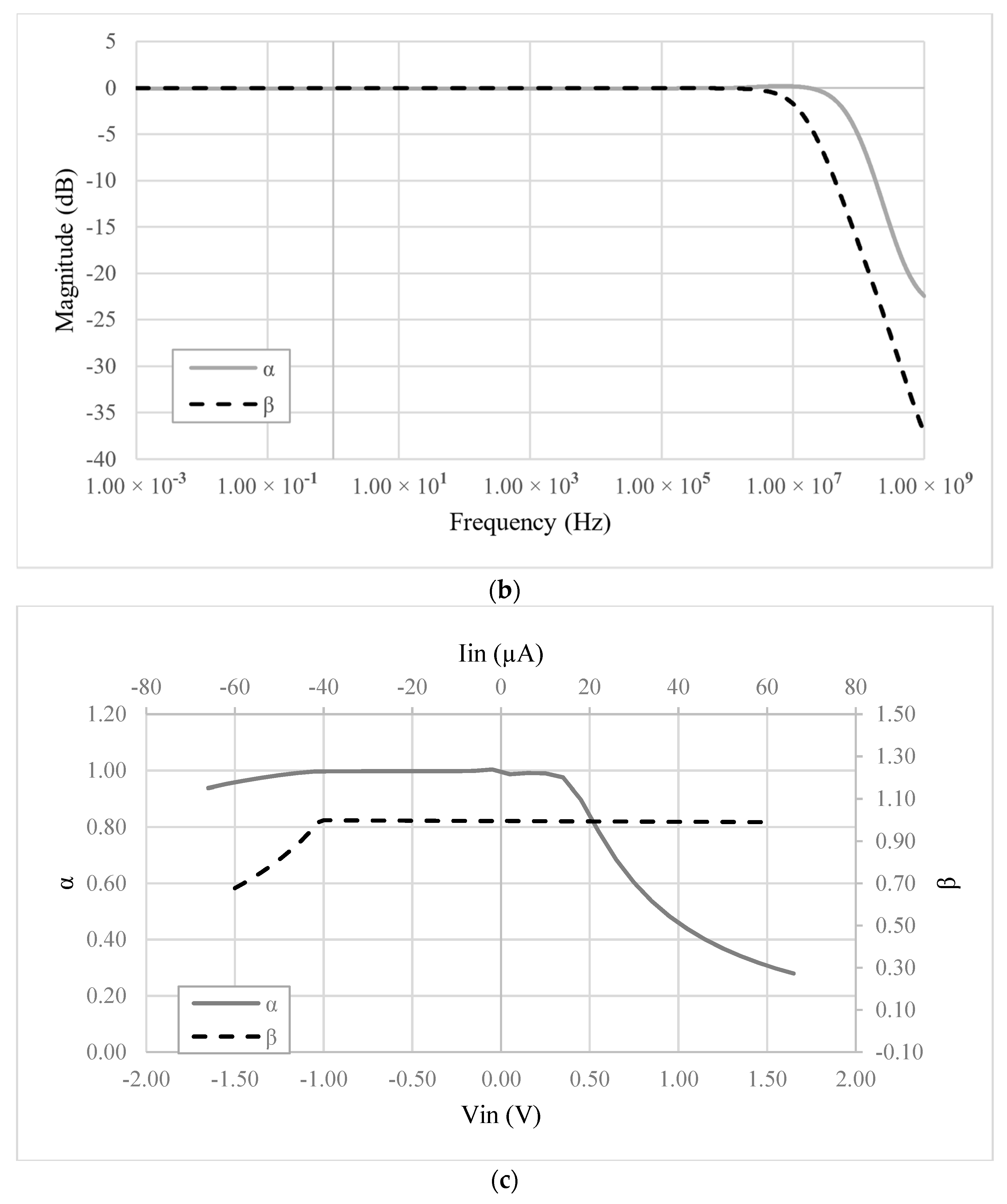
Figure 5.
Time domain output voltage with (a) compensation enabled and (b) compensation disabled.

Figure 6.
DC characteristic (|Vout| vs. |x|) of the integrated interface.
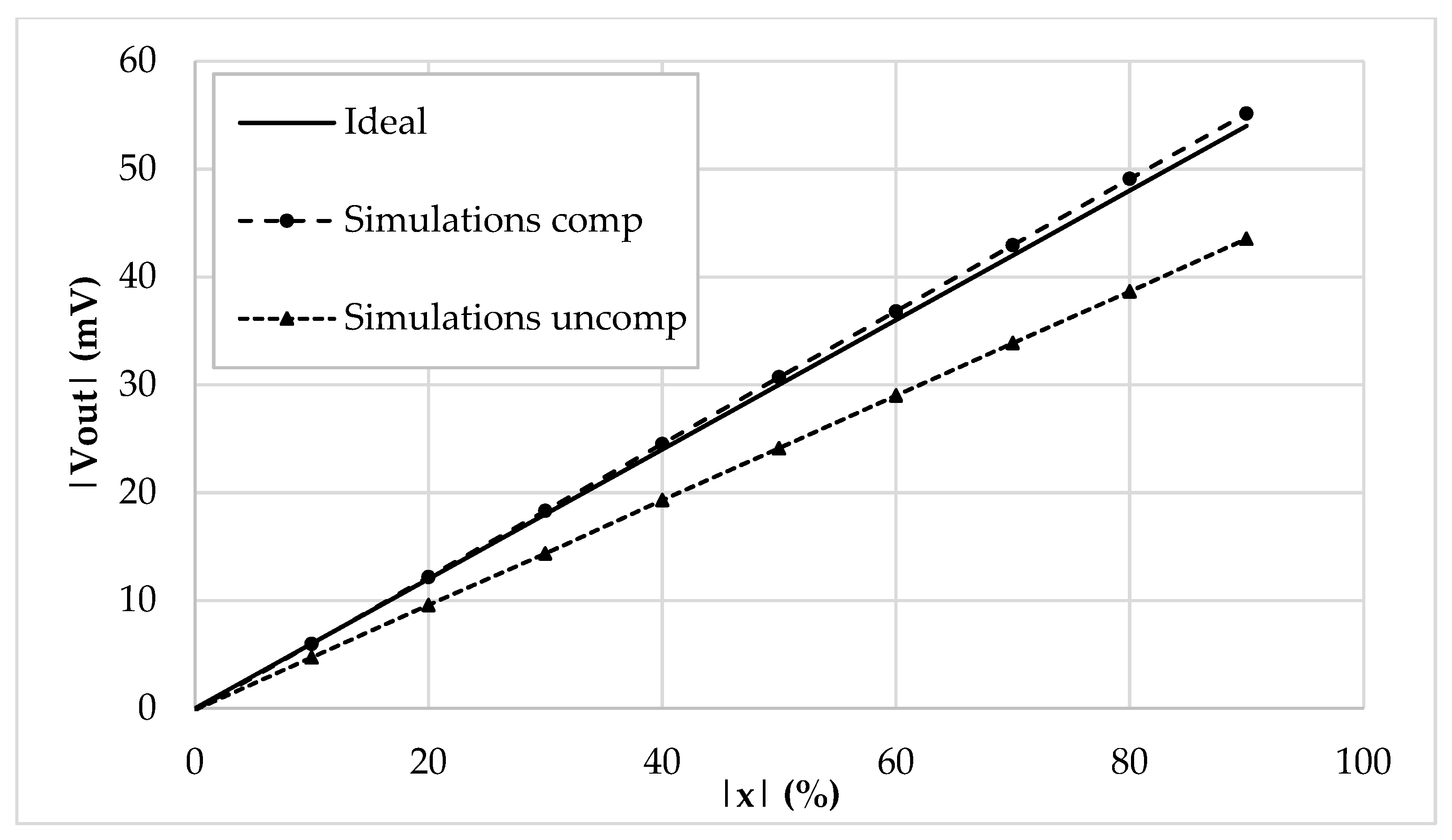
Figure 7.
Full-scale error (%) of the compensated and uncompensated integrated interface.

Figure 8.
Discrete VCII implementation.

Figure 9.
Discrete interface simulations: (a) Time domain output voltage, (b) extracted DC characteristic, (c) full-scale error (%).
Figure 9.
Discrete interface simulations: (a) Time domain output voltage, (b) extracted DC characteristic, (c) full-scale error (%).

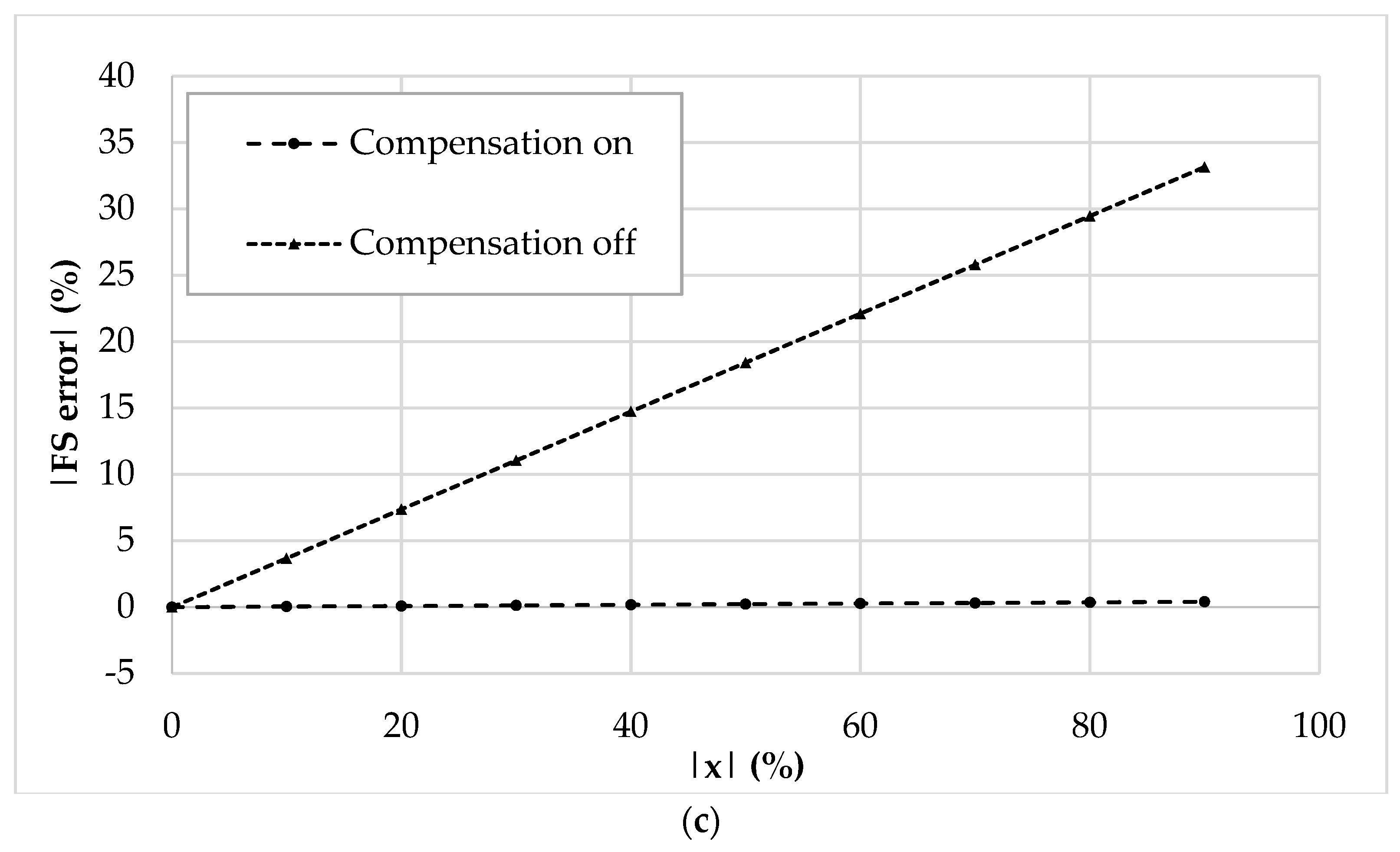
Figure 10.
The prototyped interface.

Figure 11.
Time domain output voltage of the prototyped interface.

Figure 12.
DC characteristic (|Vout| vs. |x|) of the prototyped interface.

Figure 13.
Full-scale error (%) of the compensated and uncompensated prototyped interface.

Figure 14.
DC characteristic (|Vout| vs. |x|) and full-scale error (%) of the prototyped interface with a 10 pF sensor baseline.
Figure 14.
DC characteristic (|Vout| vs. |x|) and full-scale error (%) of the prototyped interface with a 10 pF sensor baseline.


Table 1.
The used VCII parameters.
| Parameter | Value | |
|---|---|---|
| rx | 800 kΩ | |
| ry | 50 Ω | |
| rz | 80 Ω | |
| α | −43 mdB | |
| β | −45 mdB | |
| Voltage noise density at | x | 342 nV/√Hz |
| y | 420 nV/√Hz | |
| z | 118 nV/√Hz | |
| Power dissipation | 0.7 mW | |
Table 2.
Comparison table.
| Ref. | This Work | [8] | [10] | [12] | [16] | [17] | [21] |
|---|---|---|---|---|---|---|---|
| Approach | Mixed | C to V | C to I | C to V | C to V | C to Digital | C to V |
| Variation Range | ±100% | ±100% | ±100% | ±60% | ±50% | ±50% | −30%; +100% |
| Cbl | 10 pF/200 pF | 140 pF ÷ 14 nF | 1 pF | 20 pF | 500 pF | 400 pF | 400 pF |
| Linearity Error FS | <1.9%/<0.9% | 0.5 ÷ 0.8% | ±1.5% | <0.1% | <0.03% | <0.2% | <0.45% |
| Sensitivity | 412 mV/pF/21 mV/pF | 71 mV/pF | 50 nA/fF | 833 mV/pf | 5 mV/pF | 4 counts/pF | Nonlinear |
| Typology | Discrete | Discrete | Integrated | Discrete | Discrete | Discrete | Discrete |
© 2019 by the authors. Licensee MDPI, Basel, Switzerland. This article is an open access article distributed under the terms and conditions of the Creative Commons Attribution (CC BY) license (http://creativecommons.org/licenses/by/4.0/).
Share and Cite
MDPI and ACS Style
Barile, G.; Safari, L.; Ferri, G.; Stornelli, V. A VCII-Based Stray Insensitive Analog Interface for Differential Capacitance Sensors. Sensors 2019, 19, 3545. https://doi.org/10.3390/s19163545
AMA Style
Barile G, Safari L, Ferri G, Stornelli V. A VCII-Based Stray Insensitive Analog Interface for Differential Capacitance Sensors. Sensors. 2019; 19(16):3545. https://doi.org/10.3390/s19163545
Chicago/Turabian StyleBarile, Gianluca, Leila Safari, Giuseppe Ferri, and Vincenzo Stornelli. 2019. "A VCII-Based Stray Insensitive Analog Interface for Differential Capacitance Sensors" Sensors 19, no. 16: 3545. https://doi.org/10.3390/s19163545
Note that from the first issue of 2016, this journal uses article numbers instead of page numbers. See further details here.