Review

An Overview of High-k Oxides on Hydrogenated-Diamond for Metal-Oxide-Semiconductor Capacitors and Field-Effect Transistors

1
Research Center for Functional Materials, National Institute for Materials Science (NIMS), 1-1 Namiki, Tsukuba 305-0044, Ibaraki, Japan
2
Research Network and Facility Services Division, National Institute for Materials Science (NIMS), 1-2-1 Sengen, Tsukuba 305-0047, Ibaraki, Japan
*
Author to whom correspondence should be addressed.
Sensors 2018, 18(6), 1813; https://doi.org/10.3390/s18061813
Submission received: 17 April 2018 / Revised: 17 May 2018 / Accepted: 1 June 2018 / Published: 4 June 2018
(This article belongs to the Special Issue Novel Sensors Based on Metal Oxide Films and Structures)

Abstract

:
Thanks to its excellent intrinsic properties, diamond is promising for applications of high-power electronic devices, ultraviolet detectors, biosensors, high-temperature tolerant gas sensors, etc. Here, an overview of high-k oxides on hydrogenated-diamond (H-diamond) for metal-oxide-semiconductor (MOS) capacitors and MOS field-effect transistors (MOSFETs) is demonstrated. Fabrication routines for the H-diamond MOS capacitors and MOSFETs, band configurations of oxide/H-diamond heterointerfaces, and electrical properties of the MOS and MOSFETs are summarized and discussed. High-k oxide insulators are deposited using atomic layer deposition (ALD) and sputtering deposition (SD) techniques. Electrical properties of the H-diamond MOS capacitors with high-k oxides of ALD-Al2O3, ALD-HfO2, ALD-HfO2/ALD-Al2O3 multilayer, SD-HfO2/ALD-HfO2 bilayer, SD-TiO2/ALD-Al2O3 bilayer, and ALD-TiO2/ALD-Al2O3 bilayer are discussed. Analyses for capacitance-voltage characteristics of them show that there are low fixed and trapped charge densities for the ALD-Al2O3/H-diamond and SD-HfO2/ALD-HfO2/H-diamond MOS capacitors. The k value of 27.2 for the ALD-TiO2/ALD-Al2O3 bilayer is larger than those of the other oxide insulators. Drain-source current versus voltage curves show distinct pitch-off and p-type channel characteristics for the ALD-Al2O3/H-diamond, SD-HfO2/ALD-HfO2/H-diamond, and ALD-TiO2/ALD-Al2O3/H-diamond MOSFETs. Understanding of fabrication routines and electrical properties for the high-k oxide/H-diamond MOS electronic devices is meaningful for the fabrication of high-performance H-diamond MOS capacitor and MOSFET gas sensors.

1. Introduction

Due to limitation of its bandgap energy, thermal conductivity, and electron saturation velocity, Si-based electronic devices cannot meet future demands in fields of high-power, high-temperature, high-frequency, and low power loss. Wide bandgap semiconductors such as SiC, GaN, and diamond are developed to partly replace Si for next-generation power electronic devices [1,2,3]. Table 1 summarizes basic physical properties of Si, 4H-SiC, GaN, and diamond [4,5,6]. Comparing with other semiconductors in this table, diamond has the widest bandgap energy, the highest breakdown field, the largest thermal conductivity, and the largest carrier mobility. Therefore, diamond-based electronic devices are promising for the future applications in fields of high-power handling, high-temperature operation, and high-frequency switching. Meanwhile, since diamond has good chemical inertness, good biocompatibility, and a large electrochemical window, it is also a suitable candidate for applications of biosensors [7,8,9]. Additionally, diamond can also be applied in fields of ultraviolet (UV) light-emitting diodes [10], UV detectors [11], and high-temperature tolerant gas sensors [12,13,14].
Although semiconductor diamond-based devices have many potential applications, lack of shallow dopants hinders the development of them. Activation energies of boron and phosphorus doped p-type and n-type diamond are as large as 370 and 570 meV at room temperature (RT), respectively. They are much higher than the RT thermal energy of around 26 meV. Although thin heavily boron-doped diamond channel layer is promising to resolve this issue [15,16], its hole mobility is not high and growth technique still needs to be improved. A p-type hydrogenated diamond (H-diamond) channel layer is considered as another candidate to resolve this issue [17,18]. Two-dimensional hole gases are accumulated on the surface of the H-diamond caused by transfer of electrons from H-diamond to negatively surface adsorbate layer [19]. Its sheet hole density is around ~1013 cm−2. After exposing H-diamond in NO2 ambient or annealing treatment in NH3 + H2 ambient, its hole density can be enhanced to be as high as ~1014 cm−2 [20,21].
Si-, GaAs- and SiC-based metal-oxide-semiconductor (MOS) capacitor and MOS field-effect transistor (MOSFET) gas sensors have been developed greatly [22,23,24,25,26]. Gate metals (such as Pd, Pt, and Ir) have catalytic properties. They can adsorb hydrogen, ammonia, and carbon monoxide gases, leading to the generation of charges at metal/oxide interfaces, which make capacitance-voltage (C-V) curve shift in the depletion region for MOS capacitors and threshold voltage (VTH) shift for the MOSFETs [27]. Although diamond has superior properties over other semiconductors, there are rarely reports for the diamond-based MOS capacitor and MOSFET gas sensors. In order to fabricate them successfully, it is important to know the fabrication routines and electrical properties of diamond-based MOS capacitors and MOSFETs.
Recently, fabrication techniques for the H-diamond-based MOS capacitors and MOSFETs have been developed greatly. The electrical properties of them have also been improved. The H-diamond MOS capacitors with low leakage current and trapped charge densities were fabricated [28,29,30,31,32,33,34]. By improving the device structures, T-type and triple-gate fin-type H-diamond MOSFETs were fabricated successfully with current outputs more than 200 mA·mm−1 [32,33,34]. The NO2-treated H-diamond channel layer based MOSFETs could operate well with a current output as high as 1.35 A·mm−1 [35]. Improvement of deposition conditions for the oxide insulators enhanced H-diamond MOSFET’s operation temperature and breakdown voltage to be more than 400 °C and 1000 V, respectively [36]. Additionally, enhancement-mode H-diamond MOSFETs were developed for low power consumption [37,38,39].
Previously, we have focused on fabrication of high-k oxide/H-diamond MOS electronic devices [28,29,30,31,32,33]. Figure 1 shows polarization charge and sheet hole density in the H-diamond as functions of electric field [40,41], which is applied to gate oxide insulators of SiO2, Al2O3, HfO2 [42], and TiO2 [43]. At the same electric field, the oxide insulator with a higher-k value can response a larger sheet hole density for the MOS electronic devices. A gate oxide insulator with k value around 100 based on TiO2 is essential to attain hole densities around 1014 cm−2 for the H-diamond channel layer. Here, we summarize our previous reports for the Al2O3, HfO2, and TiO2 high-k oxide insulators on the H-diamond for the MOS electronic devices [28,29,30,31,44]. The oxide insulators are deposited using atomic layer deposition (ALD) and sputtering deposition (SD) techniques. Band configurations of ALD-Al2O3/H-diamond, ALD-HfO2/H-diamond, and ALD-TiO2/ALD-Al2O3/H-diamond heterojunctions are demonstrated. Electrical properties of H-diamond MOS capacitors with oxides of ALD-Al2O3 [28], ALD-HfO2 [29], ALD-HfO2/ALD-Al2O3 multilayer [28], SD-HfO2/ALD-HfO2 bilayer [30], SD-TiO2/ALD-Al2O3 bilayer [31], and ALD-TiO2/ALD-Al2O3 bilayer [31] are summarized and discussed. Analyses for the C-V characteristics of them show that there are low fixed and trapped charge densities for the ALD-Al2O3/H-diamond and SD-HfO2/ALD-HfO2/H-diamond MOS capacitors. The k value of ALD-TiO2/ALD-Al2O3 bilayer is larger than those of other oxide insulators. There are excellent electrical properties for the ALD-Al2O3/H-diamond, SD-HfO2/ALD-HfO2/H-diamond, and ALD-TiO2/ALD-Al2O3/H-diamond MOSFETs.

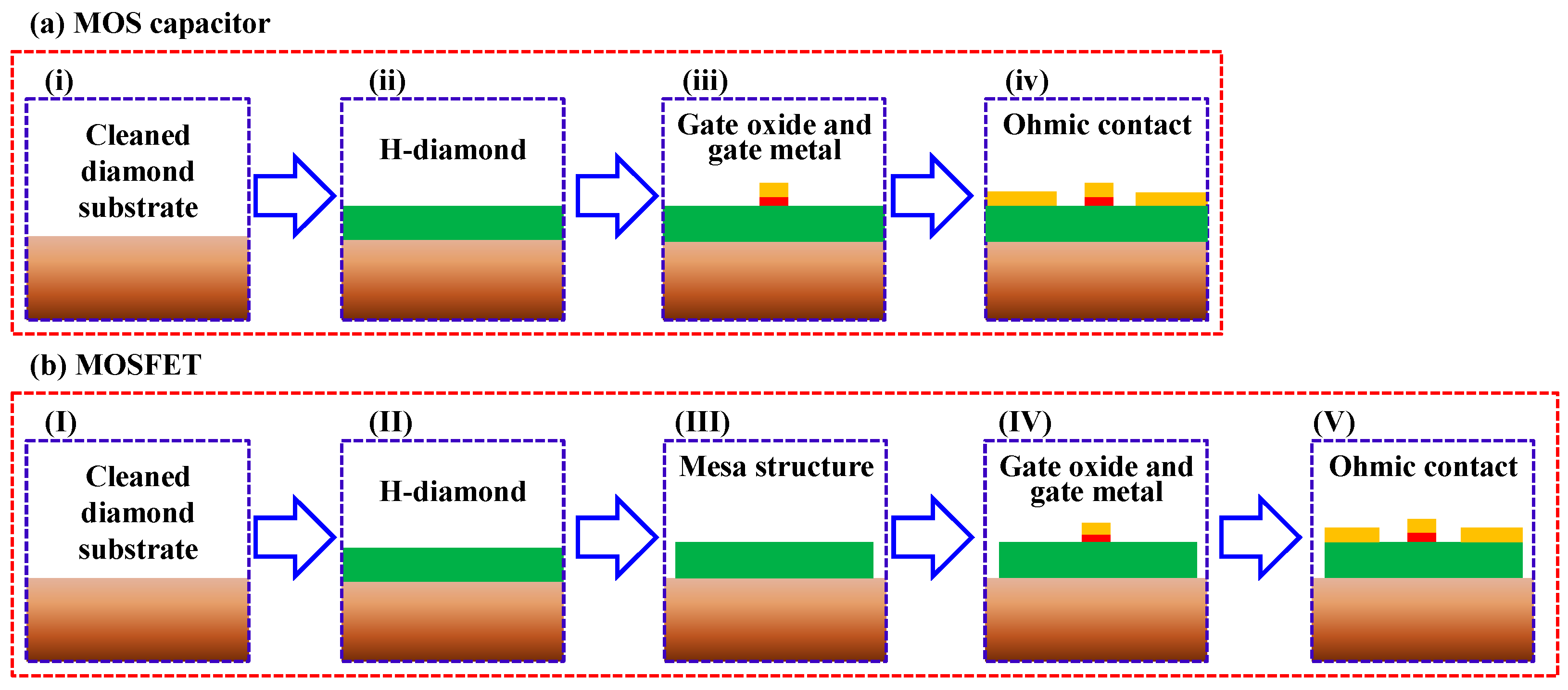
2. Materials and Methods

Figure 2a,b show fabrication routines for the H-diamond MOS capacitor and MOSFET, respectively. Ib-type single crystalline diamond (001) substrate is boiled using a hotplate in a H2SO4 and HNO3 mixture solution at 300 °C for 3 h to clean surface contaminations (Figure 2ai,bI). The H-diamond channel layer is epitaxially grown on the cleaned substrate using microwave plasma-enhanced chemical vapor deposition technique (Figure 2aii,bII). Growth gases are H2 and CH4 with flow rates of 500 and 0.5 sccm, respectively. Chamber pressure is fixed at 80 Torr. Microwave power and growth temperature are in the range of 880~960 W and 900~940 °C, respectively. Thicknesses of the H-diamond epitaxial layers are in the range of 150~200 nm. Surface roughness confirmed by atomic force microscope is around 1.2 nm [45]. The sheet hole density and mobility investigated by Hall measurement are around 1013 cm−2 and 90 cm2·V−1·s−1, respectively. After growing the H-diamond channel layer, mesa-structure is formed for the H-diamond MOSFETs (Figure 2bIII) using capacitive coupled plasma dry-etching system. The chamber pressure and etching time are 10 Pa and 90 s, respectively. Etching gas (O2) flow rate and plasma power are 100 sccm and 50 W, respectively. It should be noted that there is no mesa-structure formation step for the fabrication of oxide/H-diamond MOS capacitor. High-k oxides of the ALD-Al2O3, ALD-HfO2, ALD-HfO2/ALD-Al2O3 multilayer, SD-HfO2/ALD-HfO2 bilayer, SD-TiO2/ALD-Al2O3 bilayer, and ALD-TiO2/ALD-Al2O3 bilayer are deposited as high-k oxides for the MOS capacitors and MOSFETs (Figure 2aiii,bIV). For the SD-HfO2/ALD-HfO2 and SD-TiO2/ALD-Al2O3 bilayers, the ALD-HfO2 and ALD-Al2O3 impact as buffer layers with thicknesses of around 4.0 nm to protect the hydrogen surface from being damaged by SD plasma discharge during the SD-HfO2 and SD-TiO2 depositions, respectively. For the ALD-TiO2/ALD-Al2O3 bilayer, the ALD-Al2O3 with thicknesses of 0~4.0 nm impacts as a buffer layer to suppress high leakage current density (J) of ALD-TiO2/H-diamond MOS capacitor due to a low valence band offset (ΔEV) between TiO2 and H-diamond [42]. The ALD-Al2O3, ALD-HfO2, and ALD-TiO2 are deposited using precursors of trimethylaluminum, tetrakis (ethylmethylamino) hafnium, and tetrakis(dimethylamino)titanium with water vapor, respectively. Although the high deposition temperature for the ALD-oxides can increase their properties possibly, we have deposited them at 120 °C. There are two reasons for the low deposition temperature. Since the hydrogen surface of the H-diamond is thermal sensitivity, the low deposition temperature can protect the surface from being damaged by the heating at high temperature. Additionally, since deposition areas of oxide insulators are patterned using LOR 5A/AZ 5214E bilayer photoresists and the temperature limitation of them is 150 °C, we set the temperature of 120 °C to deposit the ALD-oxides. The SD-HfO2 layer is deposited on the ALD-HfO2/H-diamond in a pure Ar ambient at RT. The radio-frequency (RF) power, gas flow rate, and chamber pressure are 30 W, 2.0 sccm, and 1 Pa, respectively. The SD-TiO2 layer is deposited on the ALD-Al2O3/H-diamond in an Ar+O2 ambient at RT. Oxygen content in the SD chamber is in the range of 0~20%. The RF power, total gas flow rate, and chamber pressure are 40 W, 2.0 sccm, and 1 Pa, respectively. Total thickness of oxide insulators for each MOS capacitor is in the range of 18.9~34.1 nm. After depositing the oxide insulators, gate cover metals of Au/Ti or Au/Ti/Pd are formed using evaporator system. Lastly, Au/Ti/Pd triple-layer metals are evaporated on the H-diamond for the source/drain ohmic contacts (Figure 2aiv,bV).
Band configurations of oxide/H-diamond heterointerfaces are determined using X-ray photoelectron spectroscopy (XPS) technique, which is performed with a monochromated Al Kα X-ray source (hv = 1486.6 eV). All core level spectra are recorded with a 0.05 eV step and a 55 eV pass energy. Electrical properties of the MOS capacitors and MOSFETs are measured under a dark condition using MX-200/B prober and B1500A parameter analyzer at RT.

3. Results and Discussion

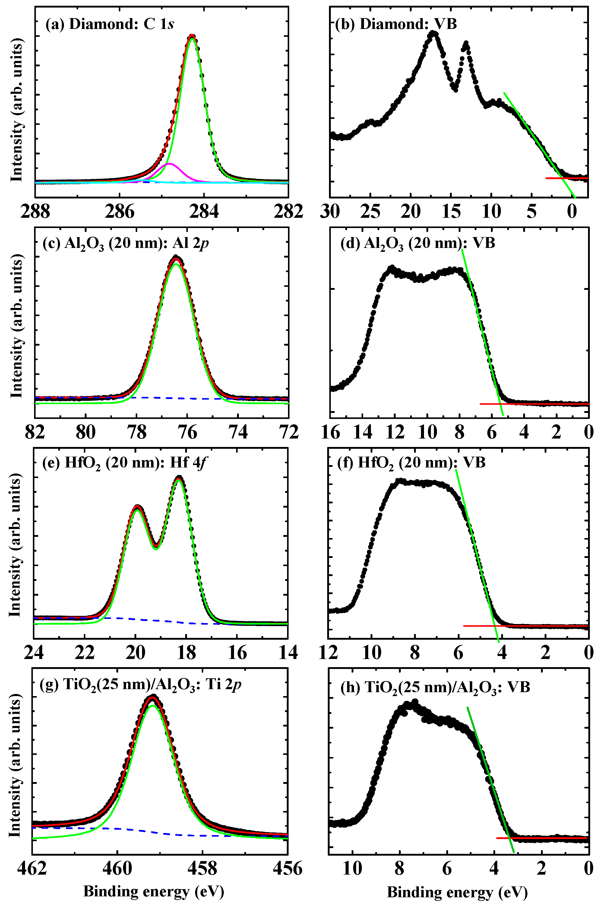
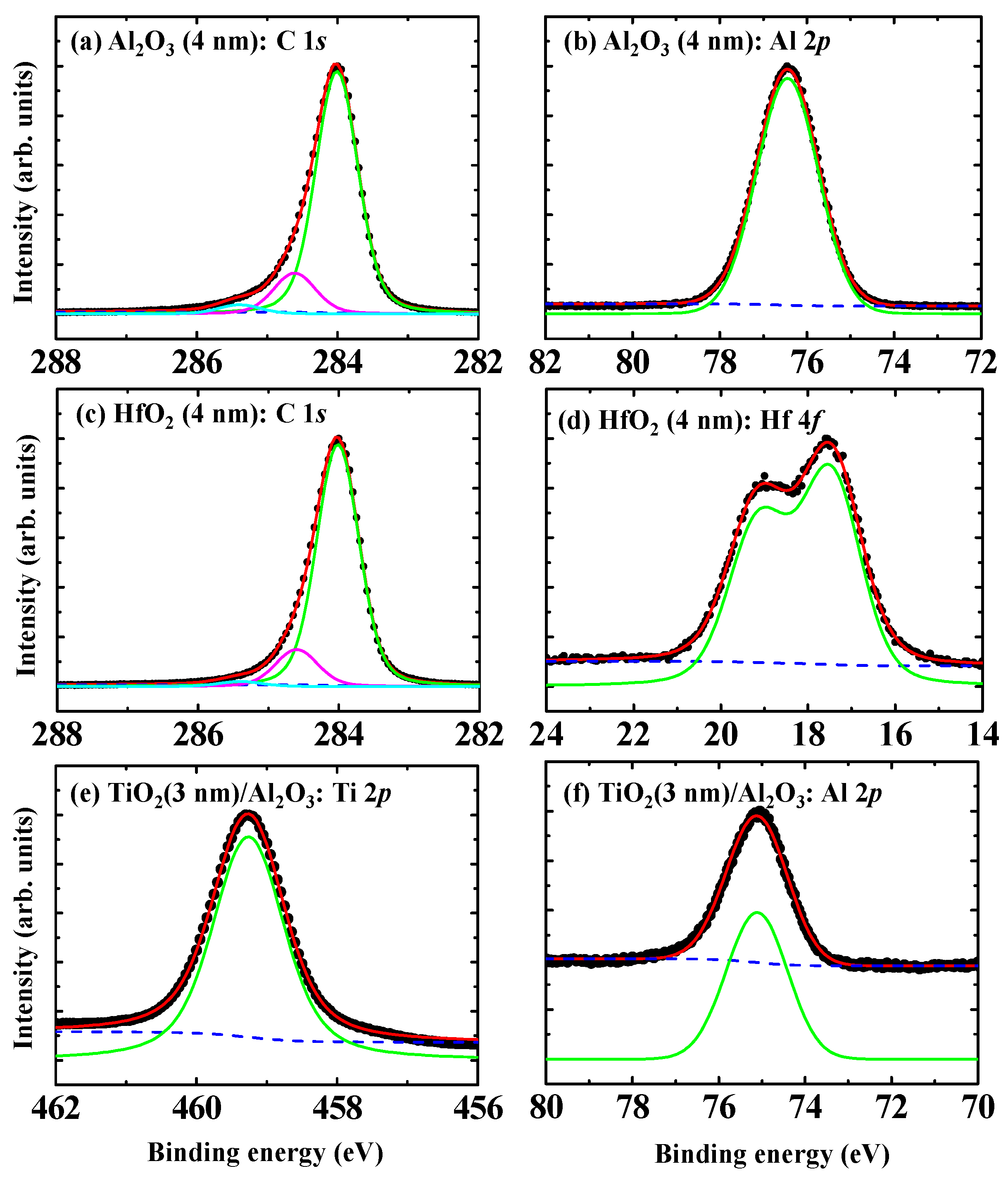
3.1. Band Configurations of High-k Oxide/H-Diamond Heterointerfaces

Band configurations of heterointerfaces are considered as the most fundamental properties in material physics. Understanding of them for high-k oxide/H-diamond heterojunctions is very important for the development of high-performance H-diamond-based MOS electronic devices. Band configurations of ALD-Al2O3/H-diamond [46], ALD-HfO2/H-diamond [46], and ALD-TiO2/ALD-Al2O3/H-diamond [31] are investigated. The ΔEV values of ALD-Al2O3/H-diamond and ALD-HfO2/H-diamond heterojunctions are calculated using the equation below,
Δ E V = ( E C L E V B M ) H d i a . ( E C L E V B M ) O x i d e T h i c k ( E C L H d i a .   E C L o x i d e ) O x i d e T h i n
where the ( E C L E V B M ) H d i a . is the difference in binding energies between C 1s core level (CL) and valence band maximum (VBM) of the H-diamond. The ( E C L E V B M ) O x i d e T h i c k is the difference in binding energies between Al 2p3/2 and VBM for the 20 nm thick Al2O3 sample or between Hf 4f7/2 and VBM for the 20 nm thick HfO2 sample. The ( E C L H d i a . E C L o x i d e ) O x i d e T h i n is the difference in binding energies between C 1s and Al 2p3/2 for the ALD-Al2O3 (4 nm)/H-diamond sample or between C 1s and Hf 4f7/2 for the ALD-HfO2 (4 nm)/H-diamond sample. The ΔEV for the ALD-TiO2/ALD-Al2O3 heterojunction can be calculated using the equation below,
Δ E V = ( E T i 2 p 3 / 2 E V B M ) T i O 2 T h i c k ( E A l 2 p 3 / 2 E V B M ) A l 2 O 3 T h i c k ( E T i 2 p 3 / 2 E A l 2 p 3 / 2 ) T i O 2 T h i n
where the ( E T i 2 p 3 / 2 E V B M ) T i O 2 T h i c k is the difference in binding energies between Ti 2p3/2 and VBM for the ALD-TiO2(25 nm)/ALD-Al2O3(4 nm) sample. The ( E A l 2 p 3 / 2 E V B M ) A l 2 O 3 T h i c k is the difference in binding energies between Al 2p3/2 and VBM for the 20 nm thick Al2O3 film [46]. The ( E T i 2 p 3 / 2 E A l 2 p 3 / 2 ) T i O 2 T h i n is the difference in binding energies between Ti 2p3/2 and Al 2p3/2 for the ALD-TiO2 (3 nm)/ALD-Al2O3 (4 nm) sample. Since calculations of the ΔEV for the ALD-Al2O3/H-diamond, ALD-HfO2/H-diamond, and ALD-TiO2/ALD-Al2O3 heterojunctions are based on the relative energies for the two peaks of each sample, there are no charge-up effects for the deduced ΔEV values.
Figure 3 shows CL and VB spectra for the H-diamond substrate (Figure 3a,b), ALD-Al2O3 (20 nm) (Figure 3c,d), ALD-HfO2 (20 nm) (Figure 3e,f), and ALD-TiO2 (25 nm)/ALD-Al2O3 (4 nm) (Figure 3g,h) measured by XPS technique. All the CL peaks are fitted using Voigt (mixed Lorentzian-Gaussian) line shapes and Shirley background. The valence band maxima of the H-diamond and thick oxide insulators are determined by extrapolating linear fitting to leading edges of the VB spectra to intersect with the baselines. The C 1s spectrum of H-diamond [Figure 3a] is fitted with three components of C-C, CHx, and C-OH [47]. Binding energy difference between C-C and CHx is 0.6 eV. That between C-C and C-OH is 1.2 eV [48]. According to angle-resolved XPS measurement result [49,50], the CHx and C-OH are attributed to surface contaminations. The Al-O (Figure 3c) and Hf-O [Figure 3e] are used to fit the Al 2p and Hf 4f spectra, respectively. The VBM values for the H-diamond, Al2O3 (20 nm), HfO2 (20 nm), and ALD-TiO2 (25 nm)/ALD-Al2O3 samples are determined to be 1.2 ± 0.2, 5.4 ± 0.2, 4.3 ± 0.2 eV, and 3.4 ± 0.2 eV, respectively.
Figure 4a,b show C 1s and Al 2p spectra for the Al2O3 (4 nm)/H-diamond sample, respectively. Figure 4c,d show C 1s and Hf 4f for the HfO2 (4 nm)/H-diamond sample, respectively. Figure 4e,f show Al 2p and Ti 2p spectra for TiO2 (3 nm)/Al2O3 (4 nm)/H-diamond sample, respectively. Three components of C-C, CHx, and C-OH are used to fit each C 1s spectrum, which is similar to those of the H-diamond substrate. The Al-O, Hf-O, and Ti-O are used to fit the Al 2p, Hf 4f, and Ti 2p spectra, respectively. Table 2 summarizes the CL peak energies and VBM values corresponding to the spectra in Figure 3 and Figure 4. The peak energies for the C 1s are relative to the C-C bonds. Binding energy error for each peak is ±0.2 V. By inserting CL binding energies and the VBM values into the Equations (1) and (2), the ΔEV values for the ALD-Al2O3/H-diamond, ALD-HfO2/H-diamond, and ALD-TiO2/ALD-Al2O3 heterojunctions are calculated to be 2.9 ± 0.2, 2.6 ± 0.2, and −0.6 ± 0.2 eV, respectively. Based on the bandgap energies of ALD-Al2O3 (7.2 eV) [46], ALD-HfO2 (5.4 eV) [46], and ALD-TiO2 (3.4 eV) [51], conduction band offset (ΔEC) values for them can be deduced to be 1.2 ± 0.2, 2.7 ± 0.2, and 3.2 ± 0.2 eV, respectively.
Figure 5a–c show band configurations of the ALD-Al2O3/H-diamond, ALD-HfO2/H-diamond, and ALD-TiO2/ALD-Al2O3/H-diamond heterojunctions, respectively. There are type II staggering-type structures for the ALD-Al2O3/H-diamond and ALD-HfO2/H-diamond heterojunctions and a type I straddling-type structure for the ALD-TiO2/ALD-Al2O3 heterojunction, respectively. The ΔEV between ALD-TiO2 and H-diamond is deduced to be 2.3 ± 0.2 eV. Because there are very large ΔEV values between the H-diamond with ALD-Al2O3, ALD-HfO2, and ALD-TiO2/ALD-Al2O3, they are promising to fabricate MOS electronic devices with low leakage current densities.

3.2. High-k Oxides on H-Diamond for MOS Capacitors

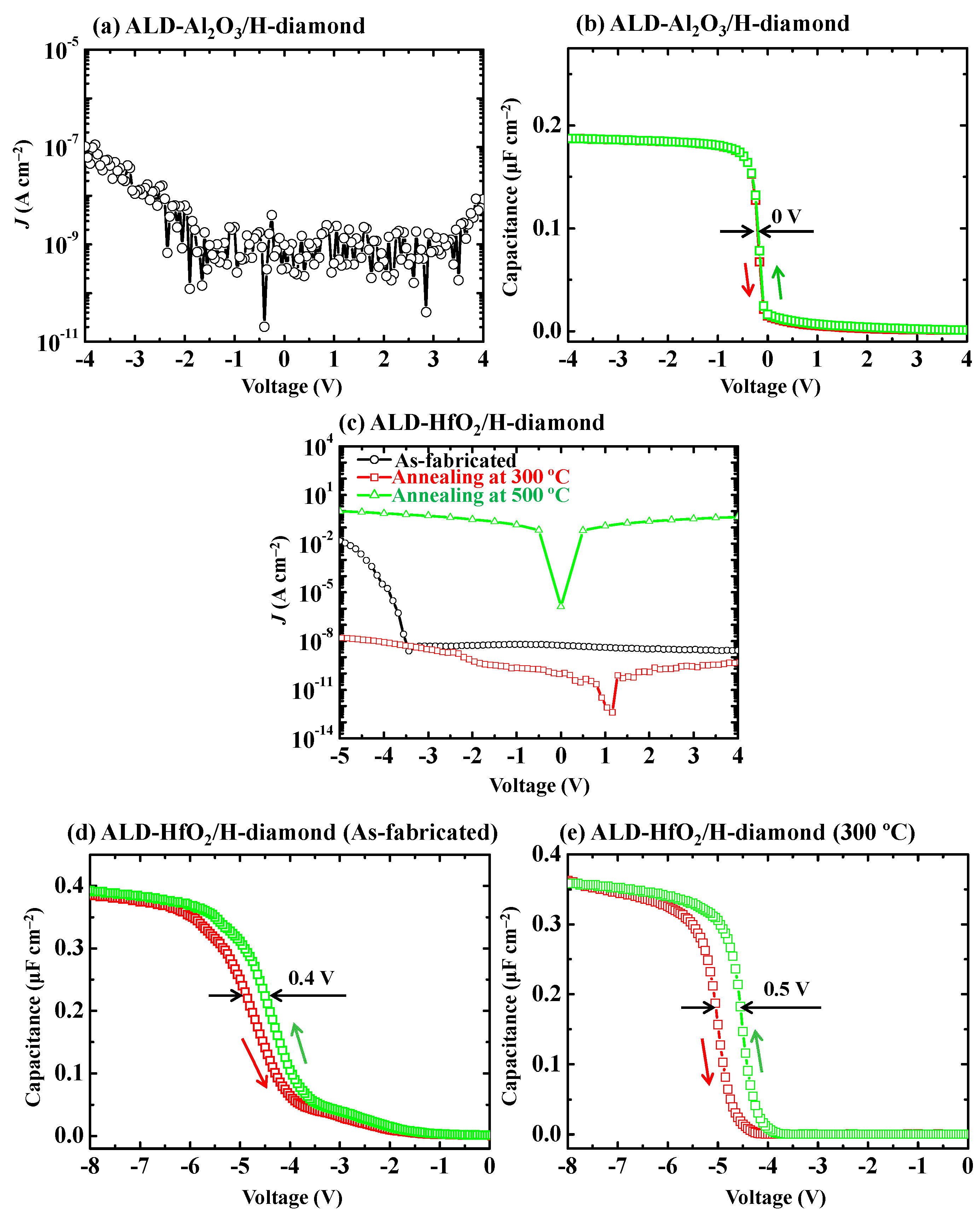
3.2.1. ALD-Al2O3 and ALD-HfO2 Single Layers

Since Al2O3 and HfO2 are two common high-k oxide insulators, electrical properties of ALD-Al2O3/H-diamond and ALD-HfO2/H-diamond MOS capacitors have been investigated firstly [28,29]. Figure 6a,b show J-V and C-V characteristics for ALD-Al2O3/H-diamond MOS capacitor, respectively. The J is deduced using leakage current divided by the gate electrode area. It is lower than 1.0 × 10⁻⁷ A·cm−2 as the gate voltage in the range of −4.0~4.0 V for the ALD-Al2O3/H-diamond MOS capacitor. Red and green lines in Figure 6b represent the C-V curves with the gate voltage sweeping directions from negative to positive and from positive to negative, respectively. Distinct accumulation region and sharp dependence at depletion region are observed in the C-V curves. Interfacial trapped charge density for the ALD-Al2O3/H-diamond is thus quite low [52]. There is a quite low voltage shift relative to 0 V in the depletion region for the C-V curves, indicating the low fixed charge density in the ALD-Al2O3 [53]. Hysteresis loop voltage for the C-V curves with the change of sweeping directions is 0 V, which suggests that there is low trapped charge density in the ALD-Al2O3 single layer. High quality Al2O3 film is thus deposited by the ALD technique at 120 °C. Maximum capacitance (Cmax) for the MOS capacitor is 0.187 μF·cm−2. By considering the ALD-Al2O3 thickness of 25.4 nm, the k value of the single ALD-Al2O3 layer can be calculated to be 5.4, which is much lower than that for the ideal Al2O3 of 8.5~9. This is possibly attributed to the low deposition temperature (120 °C) for our ALD-Al2O3 film.
Figure 6c shows annealing effect on the J-V characteristics of the ALD-HfO2/H-diamond MOS capacitors. For gate voltage higher than 0 V, the leakage current densities of the MOS capacitors before and after annealing at 300 °C are lower than 10−8 A·cm−2. For gate voltage more negative than 0 V, the J of MOS capacitor before annealing increases from 10−8 A·cm−2 at −3.4 V to 10−2 A·cm−2 at −5.0 V. However, the J after annealing at 300 °C is still lower than 1.6 × 10⁻⁸ A·cm−2. Therefore, after annealing at 300 °C, the qualities of the ALD-HfO2 film and the ALD-HfO2/H-diamond interface are improved greatly. When the annealing temperature increases to 500 °C, the large J is observed at gate voltage from −5.0 to 4.0 V, which is probably attributed to the formation of polycrystalline HfO2 film at this high temperature [54]. Figure 6d,e show C-V characteristics of ALD-HfO2/H-diamond MOS capacitors before and after annealing at 300 °C, respectively. Both C-V curves shift to the left hand sides greatly relative to 0 V, thus positive fixed charges with high densities exist in the bulk HfO2 film or close to the HfO2/H-diamond interface [53]. Both C-V curves show hysteresis loops with voltages of 0.4 and 0.5 V, respectively, which implies that there are higher trapped charge density in the bulk HfO2 film than that in the ALD-Al2O3 film, which is possibly ascribed to the oxygen vacancies in the ALD-HfO2 film. Noted that the C-V curves in the depletion regions for the ALD-HfO2/H-diamond MOS capacitor after annealing are sharper than those of before annealing and there is no residual capacitance from −1.2 V to −3.8 V in Figure 6e. Therefore, there is a lower interface trapped charge density for the ALD-HfO2/H-diamond interface after annealing than that before annealing [52]. The Cmax values for both MOS capacitors are 0.393 and 0.359 μF·cm−2, respectively. The difference is possibly ascribed to a little variation of gate electrode area during the fabrication. Based on the Cmax values and the HfO2 thickness (27.3 nm), the dielectric constants of the HfO2 films before and after annealing are calculated to be 12.1 and 11.2, respectively, which are in good agreement with the reported values (11.7~14) of ALD-HfO2 on Si and GaN substrates [54,55]. Low dielectric constants comparing with the ideal value of around 24 are believed to be the intrinsic property for the amorphous ALD-HfO2 deposited at low temperature (120 °C).

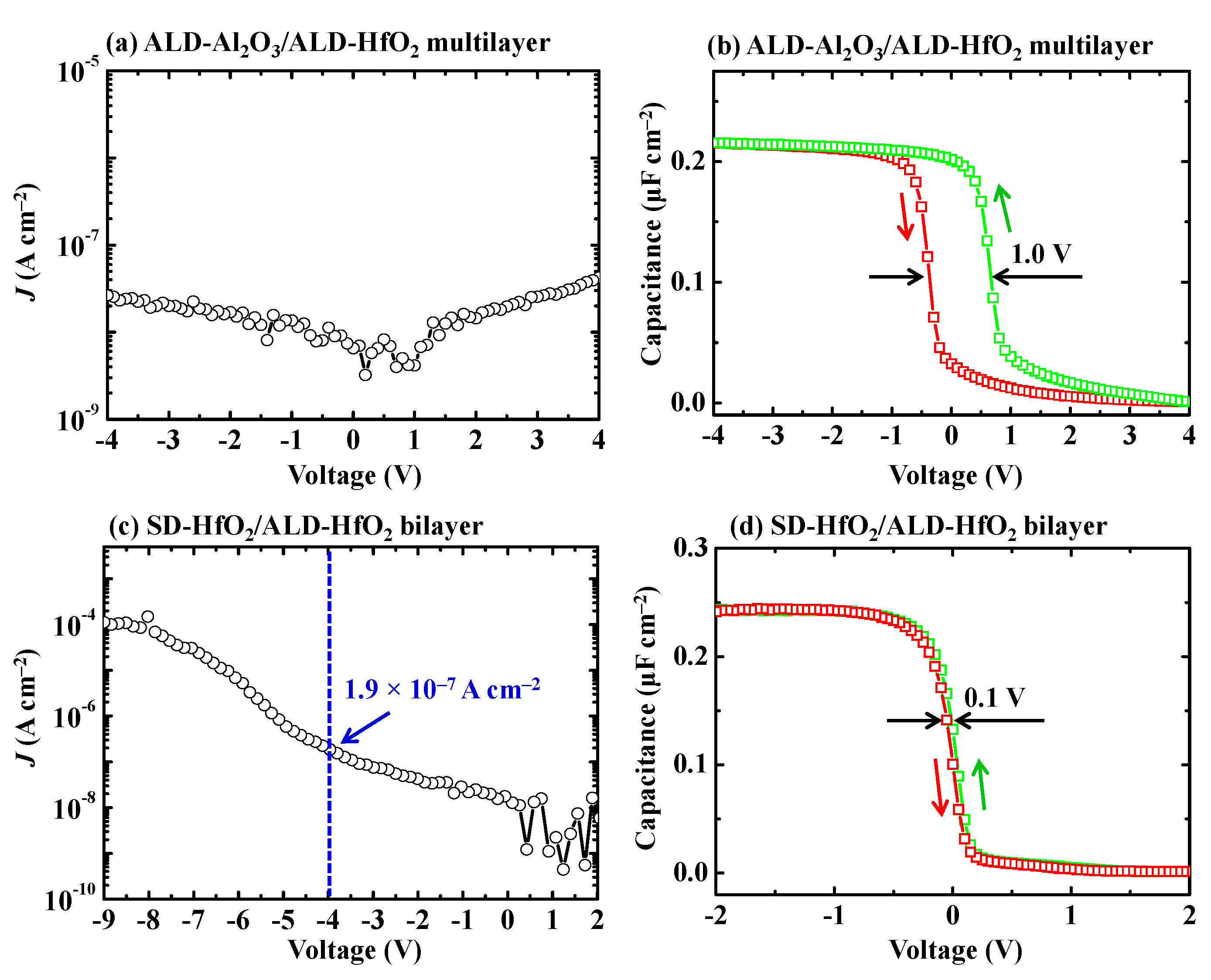
3.2.2. ALD-HfO2/ALD-Al2O3 Multilayer and SD-HfO2/ALD-HfO2 Bilayer

Since k value of the ALD-Al2O3 single layer on the H-diamond is not high and there are high positive fixed charge densities in the ALD-HfO2, we investigate electrical properties of ALD-HfO2/ALD-Al2O3 multilayer and SD-HfO2/ALD-HfO2 bilayer on the H-diamond for MOS capacitors [28,30]. Figure 7a,b show J-V and C-V characteristics for the H-diamond MOS capacitor with the ALD-Al2O3/ALD-HfO2 multilayer as the oxide insulator, respectively. The ALD-Al2O3 and ALD-HfO2 are the first and top layers in contact with the H-diamond surface and gate cover metal, respectively. Each monolayer thickness for ALD-Al2O3 and ALD-HfO2 is 1.0 nm with total thickness for the multilayer of 32.0 nm. The J for the MOS capacitor in Figure 7a at −4.0 V is 2.7 × 10⁻⁸ A·cm−2, which is lower than those of ALD-Al2O3/H-diamond and as-fabricated ALD-HfO2/H-diamond MOS capacitors. The C-V curve of the MOS capacitor in Figure 7b shows decrease of stretch-out in the depletion region compared to that for the as-fabricated ALD-HfO2/H-diamond MOS capacitor. Therefore, the interfacial trapped charge densities for the MOS capacitor with the ALD-HfO2/ALD-Al2O3 multilayer as the oxide insulator are lower than that for the as-fabricated ALD-HfO2/H-diamond MOS capacitor [53]. However, there is a large hysteresis loop voltage of around 1.0 V for the C-V curves in Figure 7b, indicating the high trapped charge density in the ALD-HfO2/ALD-Al2O3 multilayer. The Cmax for the C-V curves of the MOS capacitor is 0.216 μF·cm−2 and the k value for the HfO2/Al2O3 multilayer can be calculated to be 7.8, which is lower than that for the ALD-HfO2 single layer of 12.1 and larger than that for the ALD-Al2O3 single layer of 5.4.
Figure 7c,d show J-V and C-V characteristics for the SD-HfO2/ALD-HfO2/H-diamond MOS capacitor. The J increases with the gate voltage changing from 0 to −9.0 V. It is 1.9 × 10⁻⁷ A·cm−2 at gate voltage of −4.0 V, which is close to that of the single ALD-Al2O3/H-diamond MOS capacitor and lower than that of as-fabricated ALD-HfO2/H-diamond MOS capacitor. The maximum J value at −9.0 V is 1.1 × 10⁻⁴ A·cm−2. Based on Cmax of 0.244 μF·cm−2 and the total SD-HfO2/ALD-HfO2 thickness (34.1 nm), the k of the SD-HfO2/ALD-HfO2 bilayer is calculated to be 9.4, which is smaller than the value (12.1) of the ALD-HfO2 single layer. This is probably attributed to the low deposition temperature (at RT) for the SD-HfO2. The voltage shift relative to 0 V of the C-V curves for the SD-HfO2/ALD-HfO2/H-diamond MOS capacitor is one order magnitude lower than that for the ALD-HfO2/H-diamond MOS capacitor. Thus, the issue of high fixed charge density for the ALD-HfO2/H-diamond MOS capacitor is resolved. Additionally, the C-V curve in the depletion region shows sharp dependence and small hysteresis voltage loop of 0.1 V for the SD-HfO2/ALD-HfO2/H-diamond MOS capacitor, indicating its low trapped charge densities in the SD-HfO2/ALD-HfO2 bilayer and at the SD-HfO2/ALD-HfO2/H-diamond interfaces.

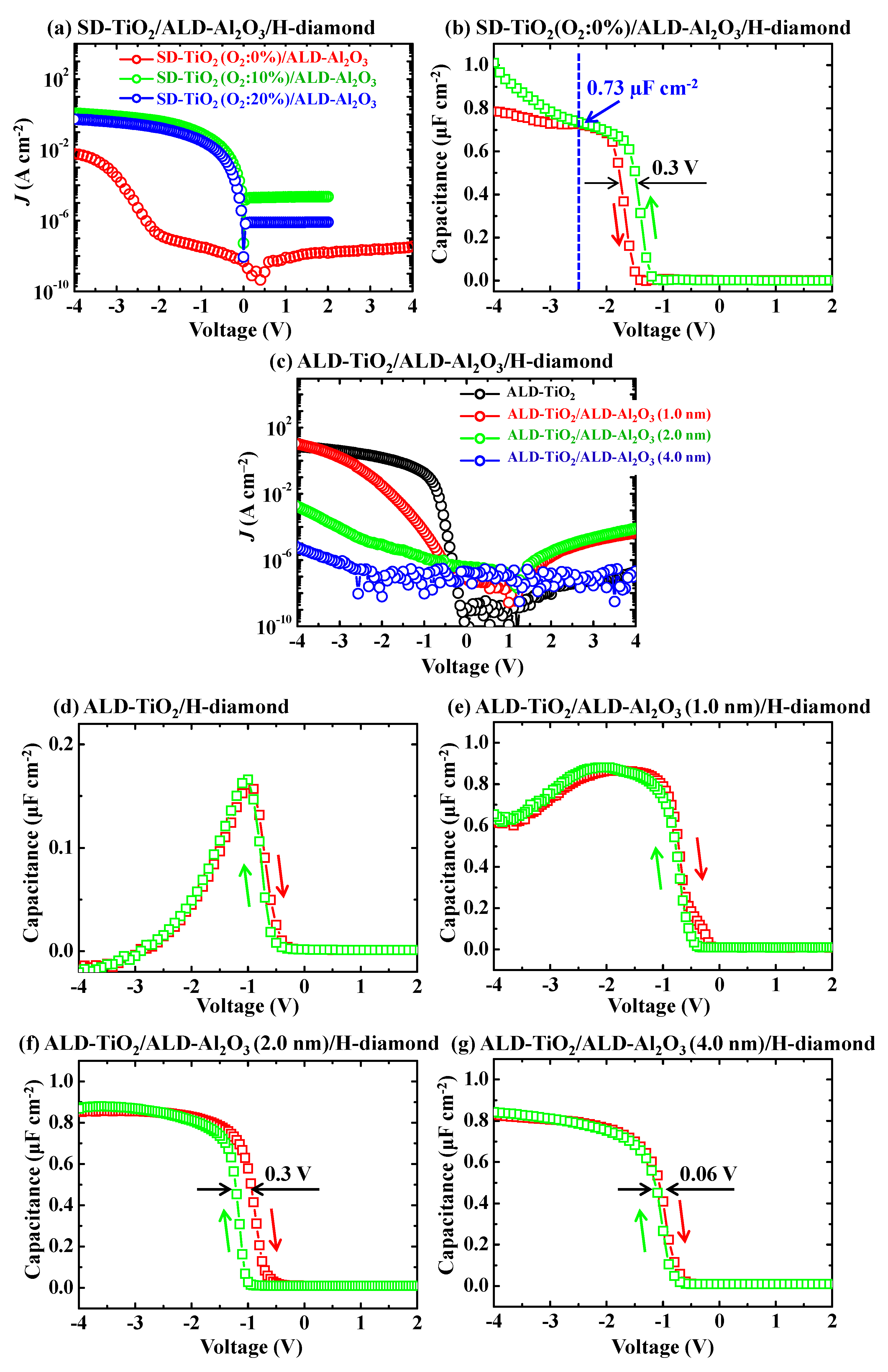
3.2.3. SD-TiO2/ALD-Al2O3 and ALD-TiO2/ALD-Al2O3 Bilayers

Figure 8a shows J-V characteristics for the SD-TiO2/ALD-Al2O3/H-diamond MOS capacitors. Thicknesses of SD-TiO2 films are 24.4, 18.9, and 23.3 nm with the change of oxygen gas content in the SD chamber of 0%, 10%, and 20%, respectively. When the chamber gas during the SD-TiO2 deposition is only Ar (O2: 0%), the J of the received MOS capacitor is lower than 10−7 A·cm−2 with the gate voltage changing from −2.0 to 4.0 V. As the gate voltage sweeps from −2.0 to −4.0 V, the J of the MOS capacitor increases from 10−7 to as large as 10−2 A·cm−2. As the oxygen gas content in the SD chamber increases to 10% and 20%, there are very high leakage current densities for the MOS capacitors. Figure 8b shows the C-V characteristic of the SD-TiO2/ALD-Al2O3/H-diamond MOS capacitor with 0% O2 content in the SD chamber during the SD-TiO2 deposition. Depletion regions of the C-V curves locate at the left hand side relative to 0 V. Thus, positive charges exist at the ALD-Al2O3/H-diamond interface or in the SD-TiO2/ALD-Al2O3 bilayer. It is clarified above that there are rarely positive charges for the ALD-Al2O3/H-diamond MOS capacitor. Therefore, the positive charges in the SD-TiO2 (O2: 0%)/ALD-Al2O3/H-diamond MOS capacitor possibly exist in the SD-TiO2/ALD-Al2O3 bilayer. When the gate voltage shifts to the left hand side relative to −2.5 V (blue dashed line), the capacitance maxima separate with the gate voltage sweeping directions, which is possibly attributed to the high J at voltage of −4.0~−2.5 V. A hysteresis loop (0.3 V) for the C-V curve is possibly ascribed to the existence of trapped charges in the SD-TiO2/ALD-Al2O3 bilayer. The Cmax for the SD-TiO2 (O2: 0%)/ALD-Al2O3/H-diamond MOS capacitor is 0.73 µF cm−2 at −2.5 V. The k value of the SD-TiO2/ALD-Al2O3 bilayer can be calculated to be 22.5.
Figure 8c shows the leakage current densities of the ALD-TiO2/ALD-Al2O3/H-diamond MOS capacitors. The ALD-TiO2 thickness for each sample is 25.0 nm. The ALD-Al2O3 buffer layer thicknesses are 0, 1.0, 2.0, and 4.0 nm, respectively. The black, red, green, and blue lines represent the J for the MOS capacitors with the ALD-Al2O3 buffer layer thickness changing from 0 to 4.0 nm, respectively. With increase of the ALD-Al2O3 buffer layer thickness, the J for the MOS capacitors decreases at gate voltage of −4.0 V. Since the EV at the ALD-TiO2/H-diamond heterointerface is low, the J for the ALD-TiO2/H-diamond MOS capacitor is quite high [41]. While there is 1.0 nm-thick Al2O3 buffer layer for the ALD-TiO2/ALD-Al2O3/H-diamond MOS capacitor, the J of it is still high due to hole tunneling effect. When the buffer layer thicknesses are 2.0 and 4.0 nm, the leakage current densities of the MOS capacitors are improved to be lower than 1.7 × 10⁻³ and 6.0 × 10⁻⁶ A·cm−2, respectively. Figure 8d–g show the C-V characteristics for ALD-TiO2/ALD-Al2O3/H-diamond MOS capacitors with ALD-Al2O3 buffer layer thicknesses of 0, 1.0, 2.0, and 4.0 nm, respectively. The depletion regions for all the C-V curves locate at left hand sides relative to 0 V. Thus, there are positive charges at the ALD-TiO2/ALD-Al2O3 bilayers [53]. In Figure 8d,e, the Cmax values decrease greatly with the gate voltages changing from −1.0 to −4.0 V and from −2.0 to −4.0 V, respectively, which are possibly attributed to their high leakage current densities. When the thickness of ALD-Al2O3 buffer layer increases to be 2.0 nm, there are distinct accumulation and depletion regions for the C-V characteristics of the MOS capacitor. However, a small hysteresis loop of 0.3 V exists. On the contrary, the hysteresis loop is only 0.06 V for the MOS capacitor with the ALD-Al2O3 buffer layer thickness of 4.0 nm. According to the Cmax value of 0.83 µF·cm−2 for the ALD-TiO2 (25.0 nm)/ALD-Al2O3 (4.0 nm)/H-diamond MOS capacitor, the k value for the ALD-TiO2/ALD-Al2O3 bilayer is deduced to be 27.2, which is larger than those of other oxide insulators on the H-diamond for the MOS capacitors.

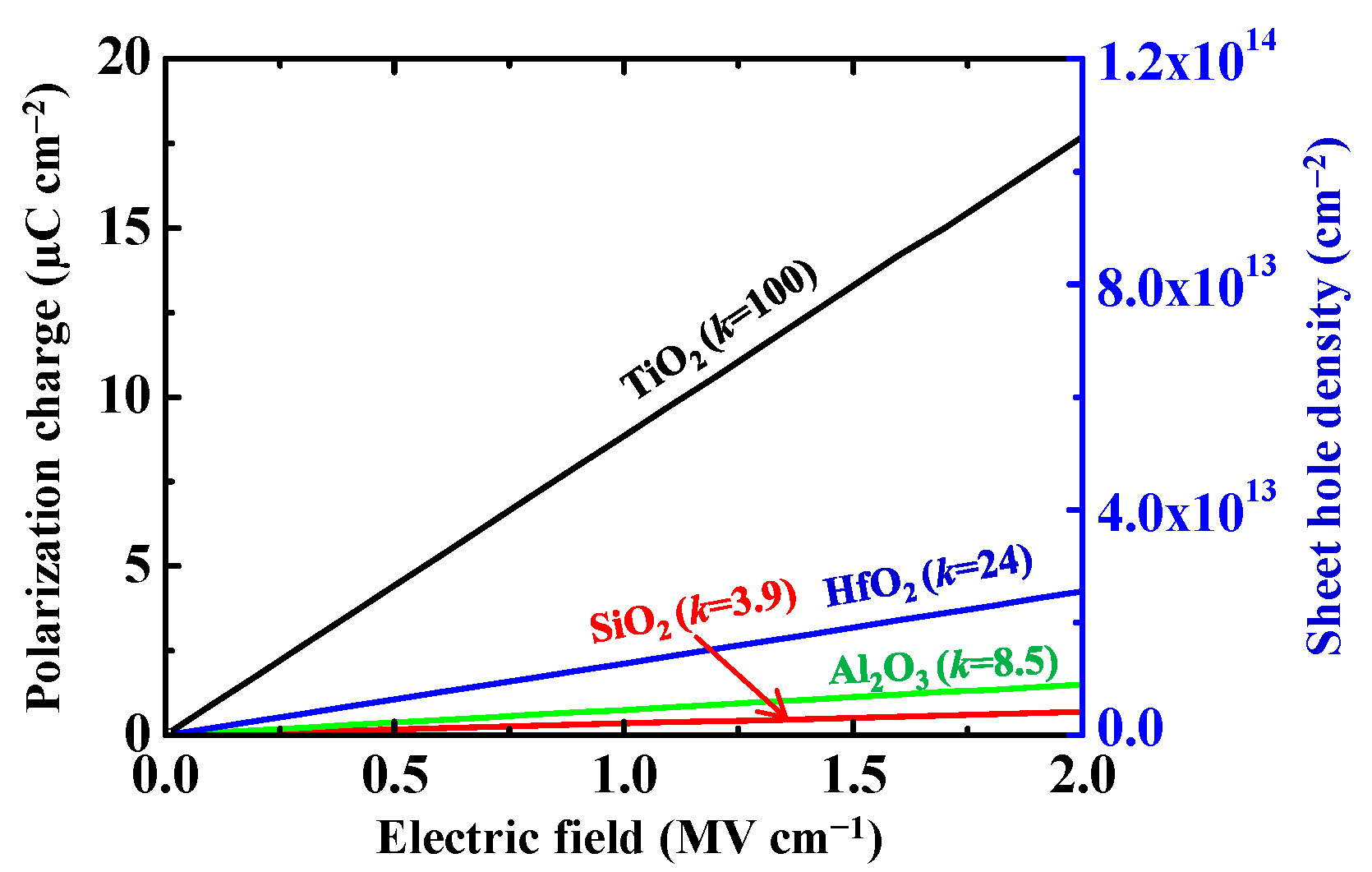
3.2.4. Discussion for High-k Oxide/H-Diamond MOS Capacitors

We have demonstrated above for the electronic properties of several high-k oxide insulators on the H-diamond for the MOS capacitors. The J at −4.0 V, k values of oxide, C-V curve hysteresis loop voltage, and C-V curve voltage shift relative to 0 V for them are summarized in Table 3. Except for SD-TiO2 (O2: 0%)/ALD-Al2O3/H-diamond MOS capacitor, the J at −4.0 V for other MOS capacitors is lower than 6.0 × 10⁻⁶ A·cm−2. The k value of ALD-TiO2/ALD-Al2O3 bilayer (27.2) is higher than those of ALD-Al2O3 (5.4), ALD-HfO2 (12.1), ALD-HfO2/ALD-Al2O3 multilayer (7.8), SD-HfO2/ALD-HfO2 bilayer (9.1), and SD-TiO2/ALD-Al2O3 bilayer (22.5). The hysteresis loop voltages for C-V curves of the ALD-Al2O3/H-diamond, SD-HfO2/ALD-HfO2/H-diamond, and SD-TiO2/ALD-Al2O3/H-diamond MOS capacitors are lower than 0.1 V, indicating their low trapped charge densities in the oxide insulators. There are large voltage shift relative to 0 V for the ALD-HfO2/H-diamond, SD-TiO2/ALD-Al2O3/H-diamond, and ALD-TiO2/ALD-Al2O3/H-diamond MOS capacitors. Since hysteresis loop of C-V curves for the MOS capacitor with ALD-HfO2/ALD-Al2O3 multilayer as oxide insulator is very large, we do not show its voltage shift relative to 0 V. There are small voltage shifts for the ALD-Al2O3/H-diamond and SD-HfO2/ALD-HfO2/H-diamond MOS capacitors, indicating their low fixed charged densities in the oxides. For the MOS capacitor gas sensors, reactions between gases and catalytic metals make charges accumulation at the metal/oxide interfaces, leading to the shift of C-V curve in the deletion region. Therefore, the best oxide insulators for the MOS capacitor gas sensors are those having low fixed and trapped charge densities. Based on the electrical properties of MOS capacitors, the ALD-Al2O3 and SD-HfO2/ALD-HfO2 bilayer are possibly two good choices for the applications of the H-diamond MOS capacitor gas sensors.

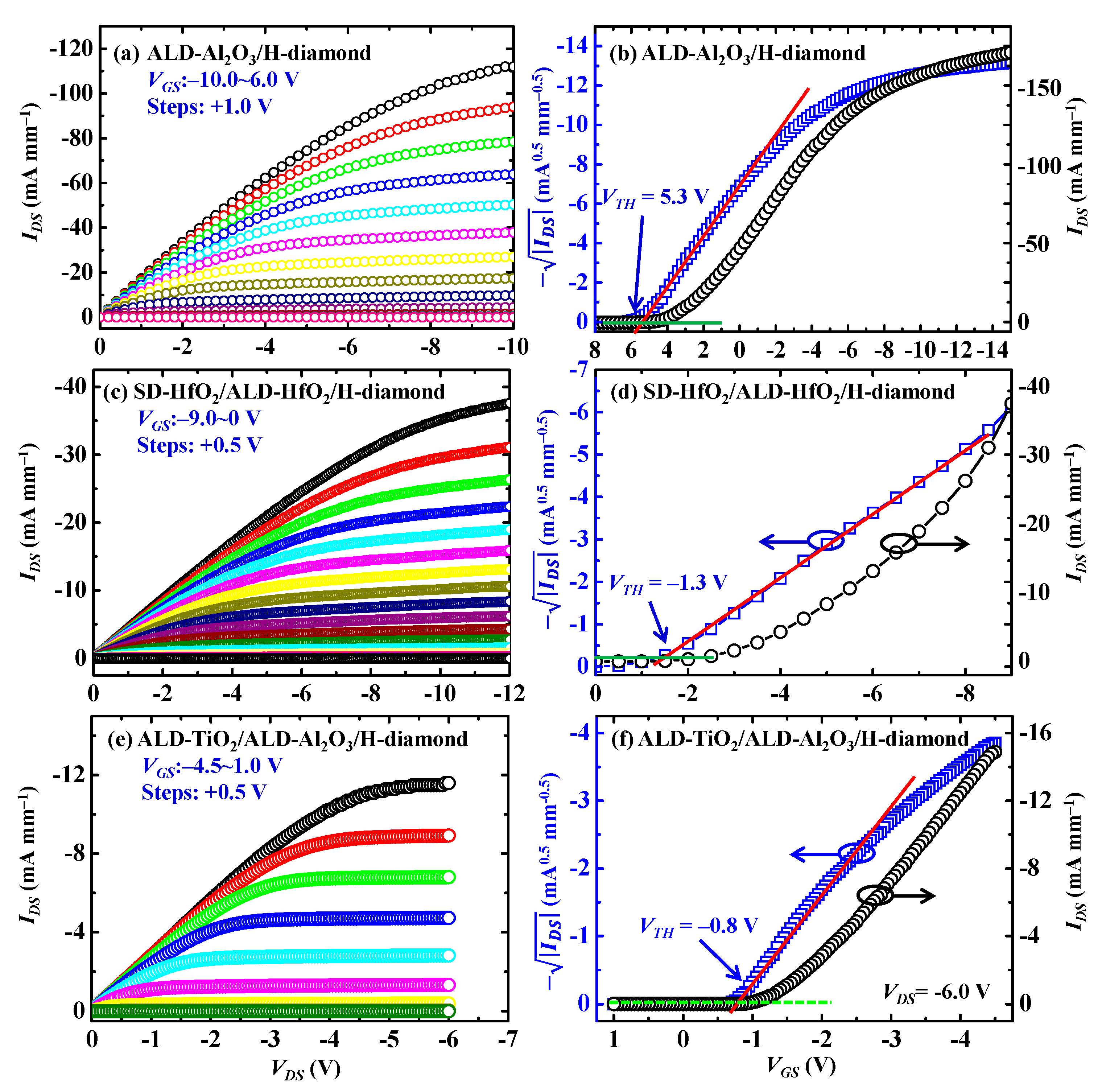
3.3. Electrical Properties of H-Diamond MOSFETs

Since there are low fixed and trapped charge densities for the ALD-Al2O3/H-diamond and SD-HfO2/ALD-HfO2/H-diamond MOS capacitors and there is the highest k value for the ALD-TiO2/ALD-Al2O3 bilayer, we will show electrical properties of the ALD-Al2O3/H-diamond, SD-HfO2/ALD-HfO2/H-diamond, and ALD-TiO2/ALD-Al2O3/H-diamond MOSFETs. Figure 9a,c,e show drain-source current versus drain voltage (IDS-VDS) characteristics for the ALD-Al2O3/H-diamond, SD-HfO2/ALD-HfO2/H-diamond, and ALD-TiO2/ALD-Al2O3/H-diamond MOSFETs, respectively. Gate length (LG) and gate width (WG) are 3 and 100 μm for the ALD-Al2O3/H-diamond MOSFET, respectively [39]. Those are 4 and 150 μm for the SD-HfO2/ALD-HfO2/H-diamond and ALD-TiO2/ALD-Al2O3/H-diamond MOSFETs, respectively [30]. Interspaces between source/drain and gate are around 1.2 ± 0.1, 5.0, and 4.0 μm for the ALD-Al2O3/H-diamond, SD-HfO2/ALD-HfO2/H-diamond, and ALD-TiO2/ALD-Al2O3/H-diamond MOSFETs, respectively. Gate-source voltage (VGS) is varied from −10.0 to 6.0 V in steps of +1.0 V for the ALD-Al2O3/H-diamond MOSFET. Those for the SD-HfO2/ALD-HfO2/H-diamond and ALD-TiO2/ALD-Al2O3/H-diamond MOSFETs are varied from −9.0 to 0 V in steps of +0.5 V and from −4.5 to 1.0 V in steps of +0.5 V, respectively. All of curves show obvious pinch-off and p-type characteristics. The maximum IDS (IDSmax) values are −112.4, −37.6, and −11.6 mA·mm−1, respectively. Difference of IDSmax for the three MOSFETs is attributed to the variations of H-diamond channel layer hole density and MOSFET device structures referring to LG, WG, and interspaces between source/drain and gate electrodes. Figure 9b,d,f show | I D S | -VGS characteristics for the ALD-Al2O3/H-diamond, SD-HfO2/ALD-HfO2/H-diamond, and ALD-TiO2/ALD-Al2O3/H-diamond MOSFETs, respectively. The VTH values of them are 5.3 ± 0.1, −1.3 ± 0.1 V, and −0.8 ± 0.1, respectively. Thus, the ALD-Al2O3/H-diamond MOSFET operate with a depletion-mode characteristic. The SD-HfO2/ALD-HfO2/H-diamond and ALD-TiO2/ALD-Al2O3/H-diamond MOSFETs operate with enhancement-mode characteristics, which indicate that there is no current output at VGS = 0 V. Hole accumulation conditions for the H-diamond channel layer are surface carbon-hydrogen bonds and negatively adsorbed layer [56,57]. Since the carbon-hydrogen bonds are very stable at the temperature lower than 250 °C, the enhancement-mode characteristics for the MOSFETs result from the disappearance of negatively adsorbed layer or the formation of positive charges at the SD-HfO2/ALD-HfO2/H-diamond and ALD-TiO2/ALD-Al2O3/H-diamond interfaces [58]. On/off ratios for all MOSFETs are higher than 108. Subthreshold swings are 138, 195, and 79 mV·dec−1 for the ALD-Al2O3/H-diamond, SD-HfO2/ALD-HfO2/H-diamond, and ALD-TiO2/ALD-Al2O3/H-diamond MOSFETs, respectively [31,39].
There is the following relationship between on-resistance (RON) and effective mobility (μeff) for the H-diamond channel layer of the MOSFETs with condition of RON and source/drain-to-gate resistance (2RSD) much higher than source/drain ohmic contact resistances.
R O N = R C H + 2 R S D = [ ( I D S V D S ) V D S = 0 ] 1 = L G W G × μ e f f × C O X × ( V G S V T H ) + 2 R S D
where the RON normalized by the WG was obtained from fitting the IDS-VDS curve. The COX is the Cmax of the oxide insulator. The 2RSD value was determined based on the linear function between the LG and RON. Since the 2RSD values for the ALD-Al2O3/H-diamond and ALD-TiO2/ALD-Al2O3/H-diamond MOSFETs were not investigated in our previous studies [31,39], we only calculate the μeff of H-diamond channel layer for the SD-HfO2/ALD-HfO2/H-diamond MOSFET [30], which is around 38.7 ± 0.5 cm2·V−1·s−1.

4. Conclusions

Here, fabrication routines for the H-diamond MOS capacitor and MOSFET, band configurations of high-k oxide/H-diamond heterointerfaces, and electrical properties of the H-diamond MOS capacitors and MOSFETs were summarized. There were high valence band offsets for ALD-Al2O3/H-diamond, ALD-HfO2/H-diamond, and ALD-TiO2/ALD-Al2O3/H-diamond heterointerfaces. Electrical properties of the H-diamond MOS capacitors with the ALD-Al2O3, ALD-HfO2, ALD-HfO2/ALD-Al2O3 multilayer, SD-HfO2/ALD-HfO2 bilayer, SD-TiO2/ALD-Al2O3 bilayer, and ALD-TiO2/ALD-Al2O3 bilayer were investigated and discussed. Except for the SD-TiO2/ALD-Al2O3/H-diamond MOS capacitor, the leakage current densities at −4.0 V for the other MOS capacitors were lower than 6.0 × 10⁻⁶ A·cm−2. The k value of ALD-TiO2/ALD-Al2O3 bilayer was 27.2, which was higher than those of other oxide insulators. There were low fixed and trapped charge densities for the ALD-Al2O3/H-diamond and SD-HfO2/ALD-HfO2/H-diamond MOS capacitors and good operations for the MOSFETs. These characteristics made them promising for the fabrication of high-performance H-diamond MOS capacitor and MOSFET gas sensors.

Acknowledgments

This work was supported by KAKENHI (No. 18K13806 and No. 16H06419) projects, Leading Initiative for Excellent Young Researchers (LEADER) program, and NIMS Nanofabrication Platform in the Nanotechnology Platform project sponsored by the Ministry of Education, Culture, Sports, and Technology, Japan.

Conflicts of Interest

The authors declare no conflict of interest.

References

  1. Bhatnagar, M.; Baliga, B.J. Comparison of 6H-SiC, 3C-SiC, and Si for power devices. IEEE Tran. Electron Dev. 1993, 40, 645–655. [Google Scholar] [CrossRef]
  2. Saito, W.; Takada, Y.; Kuraguchi, M.; Tsuda, K.; Omura, I.; Ogura, T.; Ohashi, H. High breakdown voltage AlGaN-GaN power-HEMT design and high current density switching behavior. IEEE Tran. Electron Dev. 2013, 50, 2528–2531. [Google Scholar] [CrossRef]
  3. Umezawa, H.; Nagase, M.; Kato, Y.; Shikata, S.I. High temperature application of diamond power device. Diam. Relat. Mater. 2012, 24, 201–205. [Google Scholar] [CrossRef]
  4. Wort, C.J.H.; Balmer, R.S. Diamond as an electronic material. Mater. Today 2008, 11, 22–28. [Google Scholar] [CrossRef]
  5. Gaska, R.; Shur, M.S.; Bykhovski, A.D.; Orlov, A.O.; Snider, G.L. Electron mobility in modulation-doped AlGaN-GaN heterointerfaces. Appl. Phys. Lett. 1999, 74, 287–289. [Google Scholar] [CrossRef]
  6. Trew, R.J. SiC and GaN transistors-is there one winner for microwave power applications? Proc. IEEE 2002, 90, 1032–1047. [Google Scholar] [CrossRef]
  7. Song, K.; Zhang, G.; Nakamura, Y.; Furukawa, K.; Hiraki, T.; Yang, J.; Funatsu, T.; Ohdomari, I.; Kawarada, H. Label-free DNA sensors using ultrasensitive diamond field-effect transistors in solution. Phys. Rev. E 2006, 74, 041919. [Google Scholar] [CrossRef] [PubMed]
  8. Dankerl, M.; Eick, S.; Hofmann, B.; Hauf, M.; Ingebrandt, S.; Offenhausser, A.; Stutzmann, M.; Garrido, J.A. Diamond transistor array for extracellular recording from electrogenic cells. Adv. Funct. Mater. 2009, 19, 2915–2923. [Google Scholar] [CrossRef]
  9. Nebel, C.E.; Shin, D.; Rezek, B.; Tokuda, N.; Uetsuka, H.; Watanabe, H. Diamond and biology. J. R. Soc. Interface 2007, 4, 439–461. [Google Scholar] [CrossRef] [PubMed] [Green Version]
  10. Koizumi, S.; Watanabe, K.; Hasegawa, M.; Kanda, H. Ultraviolet emission from a diamond pn junction. Science 2001, 292, 1899–1901. [Google Scholar] [CrossRef] [PubMed]
  11. Mainwood, A. Recent developments of diamond detectors for particles and UV radiation. Semicond. Sci. Technol. 2000, 15, R55–R63. [Google Scholar] [CrossRef]
  12. Gurbuz, Y.; Kang, W.P.; Davidson, J.L.; Kerns, D.V. High-temperature tolerant diamond diode for carbon monoxide gas detection. J. App. Phys. 1998, 84, 6935–6936. [Google Scholar] [CrossRef]
  13. Gurbuz, Y.; Kang, W.P.; Davidson, J.L.; Kinser, D.L.; Kerns, D.V. Diamond microelectronic gas sensors. Sens. Actuators B 1996, 33, 100–104. [Google Scholar] [CrossRef]
  14. Davidson, J.L.; Kang, W.P.; Gurbuz, Y.; Holmes, K.C.; Davis, L.G.; Wisitsora-at, A.; Kerns, D.V.; Eidson, R.L.; Henderson, T. Diamond as an active sensor material. Diam. Relat. Mater. 1999, 8, 1741–1747. [Google Scholar] [CrossRef]
  15. Pruvost, F.; Bustarret, E.; Deneuville, A. Characteristics of homoepitaxial heavily boron-doped diamond films from their Raman spectra. Diam. Relat. Mater. 2000, 9, 295–299. [Google Scholar] [CrossRef]
  16. Bustarret, E.; Gheeraert, E.; Watanabe, K. Optical and electronic properties of heavily boron-doped homo-epitaxial diamond. Phys. Status Solidi (a) 2003, 199, 9–18. [Google Scholar] [CrossRef]
  17. Strobel, P.; Riedel, M.; Ristein, J.; Ley, L. Surface transfer doping of diamond. Nature 2004, 430, 439–441. [Google Scholar] [CrossRef] [PubMed]
  18. Hayashi, K.; Yamanaka, S.; Okushi, H.; Kajimura, K. Study of the effect of hydrogen on transport properties in chemical vapor deposited diamond films by Hall measurements. Appl. Phys. Lett. 1996, 68, 376–378. [Google Scholar] [CrossRef]
  19. Pakes, C.I.; Garrido, J.A.; Kawarada, H. Diamond surface conductivity: Properties, devices, and sensors. MRS Bull. 2014, 39, 542–548. [Google Scholar] [CrossRef]
  20. Kubovic, M.; Kasu, M.; Kageshima, H.; Maeda, F. Electronic and surface properties of H-terminated diamond surface affected by NO2 gas. Diam. Relat. Mater. 2010, 19, 889–893. [Google Scholar] [CrossRef]
  21. Imura, M.; Hayakawa, R.; Watanabe, E.; Liao, M.; Koide, Y.; Amano, H. Demonstration of diamond field effect transistors by AlN/diamond heterostructure. Phys. Status Solidi (RRL) 2011, 5, 125–127. [Google Scholar] [CrossRef]
  22. Winquist, F.; Spetz, A.; Armgarth, M.; Nylander, C.; Lundström, I. Modified palladium metal-oxide-semiconductor structures with increased ammonia gas sensitivity. Appl. Phys. Lett. 1983, 43, 839–841. [Google Scholar] [CrossRef]
  23. Arbab, A.; Spetz, A.; Lundström, I. Gas sensors for high temperature operation based on metal oxide silicon carbide (MOSiC) devices. Sens. Actuators B Chem. 1993, 15, 19–23. [Google Scholar] [CrossRef]
  24. Mizsei, J. How can sensitive and selective semiconductor gas sensors be made? Sens. Actuators B Chem. 1995, 23, 173–176. [Google Scholar] [CrossRef]
  25. Arshak, K.; Moore, E.; Lyons, G.M.; Harris, J.; Clifford, S. A review of gas sensors employed in electronic nose applications. Sens. Rev. 2004, 24, 181–198. [Google Scholar] [CrossRef]
  26. Wingbrant, H.; Svenningstorp, H.; Salomonsson, P.; Kubinski, D.; Visser, J.H.; Lofdahl, M.; Spetz, A.L. Using a MISiC-FET sensor for detecting NH/sub 3/in SCR systems. IEEE Sens. J. 2005, 5, 1099–1105. [Google Scholar] [CrossRef]
  27. Spetz, A.L.; Skoglundh, M.; Ojamäe, L. FET gas-sensing mechanism, experimental and theoretical studies. In Solid State Gas Sensing; Gomini, E., Faglia, G., Sberveglieri, G., Eds.; Springer: New York, NY, USA, 2009; pp. 153–197. [Google Scholar]
  28. Liu, J.W.; Liao, M.Y.; Imura, M.; Oosato, H.; Watanabe, E.; Koide, Y. Electrical properties of atomic layer deposited HfO2/Al2O3 multilayer on diamond. Diam. Relat. Mater. 2015, 54, 55–58. [Google Scholar] [CrossRef]
  29. Liu, J.W.; Liao, M.Y.; Imura, M.; Oosato, H.; Watanabe, E.; Koide, Y. Electrical characteristics of hydrogen-terminated diamond metal-oxide-semiconductor with atomic layer deposited HfO2 as gate dielectric. Appl. Phys. Lett. 2013, 102, 112910. [Google Scholar] [CrossRef]
  30. Liu, J.W.; Liao, M.Y.; Imura, M.; Koide, Y. Normally-off HfO2-gated diamond field effect transistors. Appl. Phys. Lett. 2013, 103, 092905. [Google Scholar] [CrossRef]
  31. Liu, J.W.; Liao, M.Y.; Imura, M.; Banal, R.G.; Koide, Y. Deposition of TiO2/Al2O3 bilayer on hydrogenated diamond for electronic devices: Capacitors, field-effect transistors, and logic inverters. J. Appl. Phys. 2017, 121, 224502. [Google Scholar] [CrossRef]
  32. Liu, J.W.; Liao, M.Y.; Imura, M.; Watanabe, E.; Oosato, H.; Koide, Y. Diamond field effect transistors with a high-dielectric constant Ta2O5 as gate material. J. Phys. D Appl. Phys. 2014, 47, 245102. [Google Scholar] [CrossRef]
  33. Liu, J.W.; Liao, M.Y.; Imura, M.; Tanaka, A.; Iwai, H.; Koide, Y. Low on-resistance diamond field effect transistor with high-k ZrO2 as dielectric. Sci. Rep. 2014, 4, 6395. [Google Scholar] [CrossRef] [PubMed]
  34. Liu, J.W.; Ohsato, H.; Wang, X.; Liao, M.Y.; Koide, Y. Design and fabrication of high-performance diamond triple-gate field-effect transistors. Sci. Rep. 2016, 6, 34757. [Google Scholar] [CrossRef] [PubMed] [Green Version]
  35. Hirama, K.; Sato, H.; Harada, Y.; Yamamoto, H.; Kasu, M. Diamond field-effect transistors with 1.3 A/mm drain current density by Al2O3 passivation layer. Jpn. J. Appl. Phys. 2012, 51, 090112. [Google Scholar]
  36. Kawarada, H.; Tsuboi, H.; Naruo, T.; Yamada, T.; Xu, D.; Daicho, A.; Saito, T.; Hiraiwa, A. CH surface diamond field effect transistors for high temperature (400 °C) and high voltage (500 V) operation. Appl. Phys. Lett. 2014, 105, 013510. [Google Scholar] [CrossRef]
  37. Kitabayashi, Y.; Kudo, T.; Tsuboi, H.; Yamada, T.; Xu, D.; Shibata, M.; Matsumura, D.; Hayashi, Y.; Syamsul, M.; Inaba, M.; et al. Normally-Off C–H diamond MOSFETs with partial C–O channel achieving 2-kV breakdown voltage. IEEE Electron Dev. Lett. 2017, 38, 363–366. [Google Scholar] [CrossRef]
  38. Liu, J.W.; Oosato, H.; Liao, M.Y.; Koide, Y. Enhancement-mode hydrogenated diamond metal-oxide-semiconductor field-effect transistors with Y2O3 oxide insulator grown by electron beam evaporator. Appl. Phys. Lett. 2017, 110, 203502. [Google Scholar] [CrossRef]
  39. Liu, J.W.; Ohsato, H.; Liao, M.Y.; Imura, M.; Watanabe, E.; Koide, Y. Logic circuits with hydrogenated diamond field-effect transistors. IEEE Electron Dev. Lett. 2017, 38, 922–925. [Google Scholar] [CrossRef]
  40. Cheng, S.H.; Sang, L.; Liao, M.Y.; Liu, J.W.; Imura, M.; Li, H.; Koide, Y. Integration of high-dielectric constant Ta2O5 oxides on diamond for power devices. Appl. Phys. Lett. 2012, 101, 232907. [Google Scholar] [CrossRef]
  41. Yamasaki, S.; Gheeraert, E.; Koide, Y. Doping and interface of homoepitaxial diamond for electronic applications. MRS Bull. 2014, 39, 499–503. [Google Scholar] [CrossRef]
  42. Kordoš, P.; Gregušová, D.; Stoklas, R.; Gaži, Š.; Novák, J. Transport properties of AlGaN/GaN metal–oxide–semiconductor heterostructure field-effect transistors with Al2O3 of different thickness. Solid-State Electron. 2008, 52, 973–979. [Google Scholar] [CrossRef]
  43. Marinel, S.; Choi, D.H.; Heuguet, R.; Agrawal, D.; Lanagan, M. Broadband dielectric characterization of TiO2 ceramics sintered through microwave and conventional processes. Ceram. Int. 2013, 39, 299–306. [Google Scholar] [CrossRef]
  44. Zhao, J.; Liu, J.W.; Sang, L.W.; Liao, M.Y.; Coathup, D.; Imura, M.; Shi, B.; Gu, C.Z.; Koide, Y.; Ye, H. Assembly of a high-dielectric constant thin TiOx layer directly on H-terminated semiconductor diamond. Appl. Phys. Lett. 2016, 108, 012105. [Google Scholar] [CrossRef]
  45. Banal, R.G.; Imura, M.; Liu, J.W.; Koide, Y. Structural properties and transfer characteristics of sputter deposition AlN and atomic layer deposition Al2O3 bilayer gate materials for H-terminated diamond field effect transistors. J. Appl. Phys. 2016, 120, 115307. [Google Scholar] [CrossRef]
  46. Liu, J.W.; Liao, M.Y.; Imura, M.; Koide, Y. Band offsets of Al2O3 and HfO2 oxides deposited by atomic layer deposition technique on hydrogenated diamond. Appl. Phys. Lett. 2012, 101, 252108. [Google Scholar] [CrossRef]
  47. Vanhove, E.; De Sanoit, J.; Arnault, J.C.; Saada, S.; Mer, C.; Mailley, P.; Bergonzo, P.; Nesladek, M. Stability of H-terminated BDD electrodes: An insight into the influence of the surface preparation. Phys. Status Solidi (a) 2007, 204, 2931–2939. [Google Scholar] [CrossRef]
  48. Shi, K.; Liu, X.L.; Li, D.B.; Wang, J.; Song, H.P.; Xu, X.Q.; Wei, H.Y.; Jiao, C.M.; Yang, S.Y.; Song, H.; et al. Valence band offset of GaN/diamond heterojunction measured by X-ray photoelectron spectroscopy. Appl. Surf. Sci. 2011, 257, 8110–8112. [Google Scholar] [CrossRef]
  49. Liu, J.W.; Liao, M.Y.; Cheng, S.H.; Imura, M.; Koide, Y. Interfacial chemical bonding state and band alignment of CaF2/hydrogen-terminated diamond heterojunction. J. Appl. Phys. 2013, 113, 123706. [Google Scholar] [CrossRef]
  50. Liu, J.W.; Cheng, S.H.; Liao, M.Y.; Imura, M.; Tanaka, A.; Iwai, H.; Koide, Y. Interfacial electronic band alignment of Ta2O5/hydrogen-terminated diamond heterojunction determined by X-ray photoelectron spectroscopy. Diam. Relat. Mater. 2013, 38, 24–27. [Google Scholar] [CrossRef]
  51. Liu, G.X.; Shan, F.K.; Lee, W.J.; Shin, B.C. Growth temperature dependence of TiO2 thin films prepared by using plasma-enhanced atomic layer deposition method. J. Korean Phys. Soc. 2007, 50, 1827. [Google Scholar] [CrossRef]
  52. Deal, B.E. Standardized terminology for oxide charges associated with thermally oxidized silicon. IEEE Trans. Electron Dev. 1980, 27, 606–608. [Google Scholar] [CrossRef]
  53. Lai, B.C.M.; Kung, N.H.; Lee, J.Y.M. A study on the capacitance-voltage characteristics of metal-Ta2O5-silicon capacitors for very large scale integration metal-oxide-semiconductor gate oxide applications. J. Appl. Phys. 1999, 85, 4087. [Google Scholar]
  54. Chang, Y.C.; Chiu, H.C.; Lee, Y.J.; Huang, M.L.; Lee, K.Y.; Hong, M.; Chiu, Y.N.; Kwo, J.; Wang, Y.H. Structural and electrical characteristics of atomic layer deposited high κ HfO2 on GaN. Appl. Phys. Lett. 2007, 90, 232904. [Google Scholar] [CrossRef]
  55. Kukli, K.; Ritala, M.; Sajavaara, T.; Keinonen, J.; Leskelä, M. Comparison of hafnium oxide films grown by atomic layer deposition from iodide and chloride precursors. Thin Solid Films 2002, 416, 72–79. [Google Scholar] [CrossRef]
  56. Takeuchi, D.; Riedel, M.; Ristein, J.; Ley, L. Surface band bending and surface conductivity of hydrogenated diamond. Phys. Rev. B 2003, 68, 041304. [Google Scholar] [CrossRef]
  57. Maier, F.; Riedel, M.; Mantel, B.; Ristein, J.; Ley, L. Origin of surface conductivity in diamond. Phys. Rev. Lett. 2000, 85, 3472. [Google Scholar] [CrossRef] [PubMed]
  58. Liu, J.W.; Liao, M.Y.; Imura, M.; Matsumoto, T.; Shibata, N.; Ikuhara, Y.; Koide, Y. Control of normally on/off characteristics in hydrogenated diamond metal-insulator-semiconductor field-effect transistors. J. Appl. Phys. 2015, 118, 115704. [Google Scholar] [CrossRef]
Figure 1. Polarization charge and sheet hole density in the H-diamond as functions of electric field (Reprinted from reference [40]).
Sensors 18 01813 g001
Figure 2. Fabrication routines for H-diamond (a) metal-oxide-semiconductor (MOS) capacitor and (b) MOS field-effect transistor (MOSFET), respectively.
Sensors 18 01813 g002
Figure 3. (a) C 1s, (c) Al 2p, (e) Hf 4f, and (g) Ti 2p photoelectron spectra for the H-diamond, Al2O3 (20 nm), HfO2 (20 nm), and TiO2 (25 nm)/Al2O3 (4 nm) samples, respectively. Valence band spectra for them are also shown in Figure 3b,d,f,h, respectively (Reprinted from references [31,46]).
Sensors 18 01813 g003
Figure 4. (a,b) C 1s and Al 2p for the Al2O3 (4 nm)/H-diamond, respectively; (c,d) C 1s and Hf 4f for the HfO2 (4 nm)/H-diamond, respectively; (e,f) Al 2p and Ti 2p spectra for the TiO2 (3 nm)/Al2O3 (4 nm)/H-diamond, respectively (Reprinted from references [31,46]).
Sensors 18 01813 g004
Figure 5. Schematic band configurations for (a) ALD-Al2O3/H-diamond, (b) ALD-HfO2/H-diamond, and (c) ALD-TiO2/ALD-Al2O3/H-diamond heterojunctions, respectively (Reprinted from references [31,46]).
Sensors 18 01813 g005
Figure 6. (a,b) J-V and C-V characteristics for the ALD-Al2O3/H-diamond MOS capacitor, respectively (Reprinted from reference [28]); (c) Annealing effect on J-V characteristics of ALD-HfO2/H-diamond MOS capacitors (Reprinted from reference [29]); (d,e) C-V characteristics of the ALD-HfO2/H-diamond MOS capacitors before and after annealing at 300 °C, respectively (Reprinted from reference [29]).
Sensors 18 01813 g006
Figure 7. (a,b) J-V and C-V characteristics of the ALD-Al2O3/ALD-HfO2 multilayer on the H-diamond for MOS capacitor, respectively (Reprinted from reference [28]); (c,d) J-V and C-V characteristics for the SD-HfO2/ALD-HfO2 bilayer on the H-diamond for MOS capacitor, respectively (Reprinted from reference [30]).
Sensors 18 01813 g007
Figure 8. (a) J-V characteristics of the SD-TiO2/ALD-Al2O3/H-diamond MOS capacitors with O2 content in the SD chamber of 0%, 10%, and 20%, respectively (Reprinted from reference [31]); (b) C-V characteristics of the SD-TiO2 (O2: 0%)/ALD-Al2O3/H-diamond MOS capacitor; (c) J-V characteristics of ALD-TiO2/ALD-Al2O3/H-diamond MOS capacitors with ALD-Al2O3 buffer layer thicknesses of 0, 1.0, 2.0, and 4.0 nm, respectively; (dg) C-V characteristics of the ALD-TiO2/ALD-Al2O3/H-diamond MOS capacitors with ALD-Al2O3 buffer layer thicknesses of 0, 1.0, 2.0, and 4.0 nm, respectively (Reprinted from reference [31]).
Sensors 18 01813 g008
Figure 9. (a) IDS-VDS and (b) | I D S | -VGS characteristics for the ALD-Al2O3/H-diamond MOSFET, respectively; (c) IDS-VDS and (d) | I D S | -VGS characteristics for the SD-HfO2/ALD-HfO2/H-diamond MOSFET, respectively; (e) IDS-VDS and (f) | I D S | -VGS characteristics for the ALD-TiO2/ALD-Al2O3/H-diamond MOSFET, respectively (Reprinted from references [30,31,39]).
Sensors 18 01813 g009
Table 1. Material properties of Si, 4H-SiC, GaN, and diamond at room temperature [4,5,6].
PropertiesSi4H-SiCGaNDiamond
Bandgap energy (eV)1.123.23.45.47
Breakdown field (MV·cm−1)0.33510
Thermal conductivity (W·cm−1·K−1)1.55.01.324
Electron mobility (cm2·V−1·s−1)145090020004500
Hole mobility (cm2·V−1·s−1)4801202003800
Saturation electron velocity (×107 cm−1)0.8632.52
Saturation hole velocity (×107 cm−1)---0.8
Table 2. The binding energies (eV) of C 1s, Al 2p3/2, Hf 4f7/2, Ti 2p3/2, and VBM for the H-diamond and oxide insulators corresponding to the peaks in Figure 3 and Figure 4 [31,46].
SampleC 1sAl 2p3/2Hf 4f7/2Ti 2p3/2VBM
H-diamond284.3 1.2
Al2O3 (20 nm) 76.3 5.4
Al2O3 (4 nm)284.074.7
HfO2 (20 nm) 18.3 4.3
HfO2 (4 nm)284.0 17.5
TiO2 (25 nm)/Al2O3 459.23.4
TiO2 (3 nm)/Al2O3 75.0 459.3
Table 3. Electrical properties of high-k oxide/H-diamond MOS capacitors.
Oxide InsulatorsJ at −4.0 V (A·cm−2)kHysteresis Loop Voltage (V)Voltage Shift Related to 0 V (V)
ALD-Al2O31.0 × 10−75.40small
ALD-HfO2 (300 °C annealing)8.5 × 10−911.20.5large
ALD-HfO2/ALD-Al2O3 multilayer2.7 × 10−87.61.0-
SD-HfO2/ALD-HfO2 bilayer1.9 × 10−79.10.1small
SD-TiO2 (O2: 0%)/ALD-Al2O3 bilayer1.0 × 10−222.50.3large
ALD-TiO2/ALD-Al2O3 (4 nm) bilayer6.0 × 10−627.20.06large

