A New Design of a Single-Device 3D Hall Sensor: Cross-Shaped 3D Hall Sensor

1
School of Physics, Nanjing University, Nanjing 210093, China
2
School of Electric Science & Engineering, Nanjing University, Nanjing 210093, China
*
Author to whom correspondence should be addressed.
Sensors 2018, 18(4), 1065; https://doi.org/10.3390/s18041065
Submission received: 5 March 2018
/
Revised: 30 March 2018
/
Accepted: 30 March 2018
/
Published: 2 April 2018
(This article belongs to the Special Issue Magnetic Sensors)
Abstract
:In this paper, a new single-device three-dimensional (3D) Hall sensor called a cross-shaped 3D Hall device is designed based on the five-contact vertical Hall device. Some of the device parameters are based on 0.18 μm BCDliteTM technology provided by GLOBALFOUNDRIES. Two-dimensional (2D) and 3D finite element models implemented in COMSOL are applied to understand the device behavior under a constant magnetic field. Besides this, the influence of the sensing contacts, active region’s depth, and P-type layers are taken into account by analyzing the distribution of the voltage along the top edge and the current density inside the devices. Due to the short-circuiting effect, the sensing contacts lead to degradation in sensitivities. The P-type layers and a deeper active region in turn are responsible for the improvement of sensitivities. To distinguish the P-type layer from the active region which plays the dominant role in reducing the short-circuiting effect, the current-related sensitivity of the top edge (Stop) is defined. It is found that the short-circuiting effect fades as the depth of the active region grows. Despite the P-type layers, the behavior changes a little. When the depth of the active region is 7 μm and the thickness of the P-type layers is 3 μm, the sensitivities in the x, y, and z directions can reach 91.70 V/AT, 92.36 V/AT, and 87.10 V/AT, respectively.
1. Introduction
In recent years, Hall sensors based on CMOS (Complementary Metal-Oxide-Semiconductor Transistor) technology have been widely used in manufacturing, electronics, aerospace, and other fields due to their low cost, high integration, and reliability. Meanwhile, in the field of scientific research, Hall sensors as an effective means of converting a magnetic field into an electrical signal are also attracting more and more attention [1,2,3,4].
In order to realize the measurement of a magnetic field in the x, y, and z directions, multiple horizontal Hall devices are placed in different directions [5,6]. However, the drawbacks of this method are the complicated package and the high cost. To solve these problems, horizontal and vertical Hall devices were integrated into the same chip [7,8,9,10,11,12]. Besides this, in virtue of different biases, a single device can be also used for the measurement [13,14,15,16]. Current-related sensitivity (SI), a main performance parameter of Hall sensors, is related to the doping concentration of the active region and the thickness parallel to the magnetic field. Meanwhile, adding P-type layers will allow sensitivity promotions for Hall sensors [4]. Due to the presence of the P-type layers, PN junctions are formed between the P-type and N-type regions so that the current near the top edge is compelled to flow along the PN junctions. This brings about positive effects for the sensitivities. Since the magnetic field components Bx, By, and Bz are perpendicular to each other, the requirements for the thickness of the active region are distinct. In addition, the performance of single-device 3D Hall sensors cannot be optimized simultaneously in all three directions. Therefore, it is essential to select a suitable technology parameter to maintain balance for the entire device. The finite element method (FEM) divides a problem or structure into smaller, simpler parts and make it easier to solve the problem. COMSOL is a FEM simulation software in which the geometric and process parameters of Hall sensors can be easily varied for further analysis. The 2D and 3D models can be chosen from diverse modules to perform the studies, such as AC/DC and semiconductor modules [17,18,19]. Besides this, the relationships between the temperature and sensitivities can be investigated by considering the temperature coefficient [17,20]. COMSOL simulation results can also be used to compare with the Verilog-A model implemented in Cadence [21]. The variety of functions in COMSOL provides an easy-to-use method for the performance prediction of Hall sensors.
This work designs a new three-contact vertical Hall device which derives from the five-contact vertical Hall device [22,23]. Three-contact vertical Hall devices have served as vertical Hall Magnetic Sensors, such as the four-folded three-contact structure. Compared with the five-contact, four-contact, and six-contact vertical Hall devices, the four-folded three-contact can be compatible with various offset cancellation techniques for horizontal Hall devices [24,25,26]. Herein, two orthogonal three-contact vertical Hall devices are integrated to construct a cross-shaped 3D Hall sensor which can be used to measure the magnetic field in 3D space by different biases. The aim of this work is to discuss the behavior of the cross-shaped 3D Hall sensor through an analysis of FEM calculations. Some of the device parameters are based on 0.18 μm BCDliteTM technology provided by GLOBALFOUNDRIES. Section 2 introduces the shift from a five-contact to a three-contact vertical Hall device and the basic principle of the three-contact device for measuring the magnetic field parallel to the device. Section 3 studies the cross-shaped 3D Hall device composed of two cross-like three-contact vertical Hall devices. Section 4 investigates the respective influences of the active region and P-type layers on the current-related sensitivity. Section 5 summarizes all of the work and presents conclusions.
2. Five-Contact to Three-Contact Vertical Hall Device
Figure 1 depicts the shift from a five-contact to a three-contact vertical Hall device. The five-contact vertical Hall device is sensitive to the magnetic field parallel to the device plane. C1, C3, and C5 are the biasing contacts, while C2 and C4 are the sensing contacts. Two orthogonal five-contact vertical Hall devices in a cross shape can be used to measure the x and y components of the magnetic field. If C2, C3, and C4 are ignored, the device can serve as a cross-like horizontal Hall device. However, the measuring method is fairly complex, and the presence of C2, C3, and C4 contacts will cause a severe short-circuiting effect. This because the doping concentration at the contacts is higher than that at the active region. The conductivity of an isotropic and homogeneous conductor is given by
where σ represents the conductivity, n represents the carrier densities, and μ represents carrier mobility. It is easy to find that the conductivity increases with the doping concentration, even though the carrier mobility declines. In COMSOL, the material of the contacts is set as copper. Due to the higher conductivity at the contacts, the biasing current tends to flow to these areas, which would cause a short-circuiting effect. Converting a five-contact to a three-contact vertical Hall device can reduce the short-circuiting effect as well as the complexity by decreasing the number of contacts.
To make up a three-contact vertical Hall device, the five-contact device is divided into two halves and C2 is placed in the middle of the device. Then, a new contact C3 is placed at the symmetrical position of C1 with respect to C2 to construct a new device. The new device is called a three-contact vertical Hall device. Table 1 lists the comparisons between five-contact and three-contact vertical Hall devices, where the characteristics are physical symbols instead of detailed information. Because the three-contact vertical Hall device directly halves the length of the five-contact vertical Hall device, this will cause double power consumption of the device when biased by identical currents. To detect the magnetic field parallel to it, the three-contact vertical Hall device needs to be applied using opposite biases. Thus, the recognition rate is limited compared with the five-contact vertical Hall device. When biased by reverse currents, the deflection of the moving charge carriers due to the magnetic field is opposite. A potential difference at C2 is the Hall voltage of the three-contact vertical Hall device.
In COMSOL, the magnetic field is set as a constant, 1T. A 2D model is preferred over a 3D model for the ease of constructing a three-contact vertical Hall device. Meanwhile, C1, C2, and C3 are set as the Terminal, Floating Potential, and Ground, respectively. The biasing current is applied to the three-contact vertical Hall device via the biasing contacts-C1 and C3. For the purpose of investigating the influence of sensing contact on the behavior of the three-contact vertical Hall device, a point-like sensing contact (without C2) is placed at the center of the device, and then a 1 μm × 3 μm × 0.133 μm sensing contact C2 takes up this position. The two different structures are depicted in Figure 2a,b, respectively. Main simulation parameters are listed in Table 2. Figure 3a shows the voltage along the top edge of the device under different biases and 3b shows the distribution of voltage near C2. If the sensing contact is a point or neglected, the device’s Hall voltage is 14.68 mV. When the sensing contact is present, as shown in Figure 4, the device’s Hall voltage falls from 14.68 mV to 5.70 mV. This loss demonstrates a direct link between the sensing contact and sensitivities.
For further improvement of the sensitivities, P-type layers described in Figure 2c are put between C1 (C3) and C2. In COMSOL, the P-type layers can be simply set to a material with zero conductivity to imitate the hindrance of the PN junctions to the biasing current. Judging from Figure 4 and Figure 5, the Hall voltage augments from 5.70 mV to 5.94 mV with an increasing rate of 4.2%. This indicates that an extra P-type layer can fortify sensors against the short-circuiting effect. To get a whole picture of the three different structures, the current-related sensitivity of the top edge, Stop, is defined as shown below:
where the Vtop is voltage along the top edge. Stop can be utilized to distinguish a P-layer from the active region to see which plays the dominant role in suppressing and weakening the short-circuiting effect. With Stop, the current-related sensitivity of the three-contact vertical Hall device is given by
where C1 → C3 and C3 → C1 represent the reverse biases. The changing curves of Stop are shown in Figure 6. In comparison with Figure 3, Figure 4 and Figure 5, the sensitivity change can now be calculated immediately on the basis of Figure 6. The absolute value of Stop has a swift fall at C2, corresponding to the great loss in SI. Besides this, Stop increases slightly due to the presence of P-type layers.
The impacts of the sensing contact and P-type layers are both taken into account by inspecting the distribution of the current density. Figure 7 shows the effects of sensing contacts and P-type layers on the distribution of current density when the device is 1.018 μm deep and the P-type layers are 0.133 μm deep. Figure 7d selects some lines of current density near the top edge for more precise comparisons. Comparing Figure 7b,c with Figure 7a, we can find that the short-circuiting effect caused by the sensing contact prevails. In addition, the current is forced to flow along the boundaries of the P-type layer, as shown in Figure 7c, to reduce the effect. We infer that if a current can flow into the deep part of the Hall sensors, the behavior of the biasing current will be restrained. It is then expected that a device with intermediate depth and adjustable P-type layers may contribute to short-circuiting effect reduction. To further check this hypothesis, we study the comparisons in the distribution of the current density when the device is 3 μm deep and the P-type layers are 1 μm deep, which is shown in Figure 8. The biasing current stays away from the C2 contact compared with the device with depth 1.018 μm, even though there are no P-type layers. Meanwhile, it is obvious that the behavior will be better when the P-type layers are existent. Through an analysis of FEM calculations in COMSOL, it turns out that the current-related sensitivity rises by 18.8%, from 11.22 V/AT to 13.33 V/AT.
Figure 9 shows the current-related sensitivity of the top edge at different depths. It is justified that the deeper active region itself can cause degradation of the short-circuiting effect by preventing the biasing current from getting close to the sensing contact and making the voltage along the bottom edge become constant to compensate for the wasted Hall voltage [27]. We can even believe that if there is no sensing contact, the depth of the active area would have no effect on the sensitivities.
3. Performance of the Cross-Shaped 3D Hall Device
To accommodate measurement of the magnetic field in 3D space, two three-contact vertical Hall devices are placed orthogonally. Each of them can be used to detect the components Bx and By. When ignoring the sensing contact, the device can be regarded as a horizontal Hall device to measure Bz. The cross-shaped 3D Hall device is equivalent to the horizontal Hall device with an extra contact C0, which is depicted in Figure 10. Table 3 lists the main simulation parameters of the cross-shaped Hall device.
To discuss the differences between the horizontal Hall device and the cross-shaped 3D Hall device, Bx and By are set to 0 and Bz is set to 1T. Figure 11 depicts the voltage distribution of the Hall devices in the 3D space and x, y plane for developing a sense of the whole. The horizontal Hall device is on the top, and the cross-shaped 3D Hall device is on the bottom. Despite the introduction of the sensing contact C0, the voltage distribution of the device in all directions shows almost no change. Hence, the cross-shaped 3D Hall devices can be employed as horizontal sensors. However, due to the short-circuiting effect caused by C0, the current-related sensitivity in the z direction alters from 44.23 V/AT to 40.47 V/AT, as shown in Figure 12.
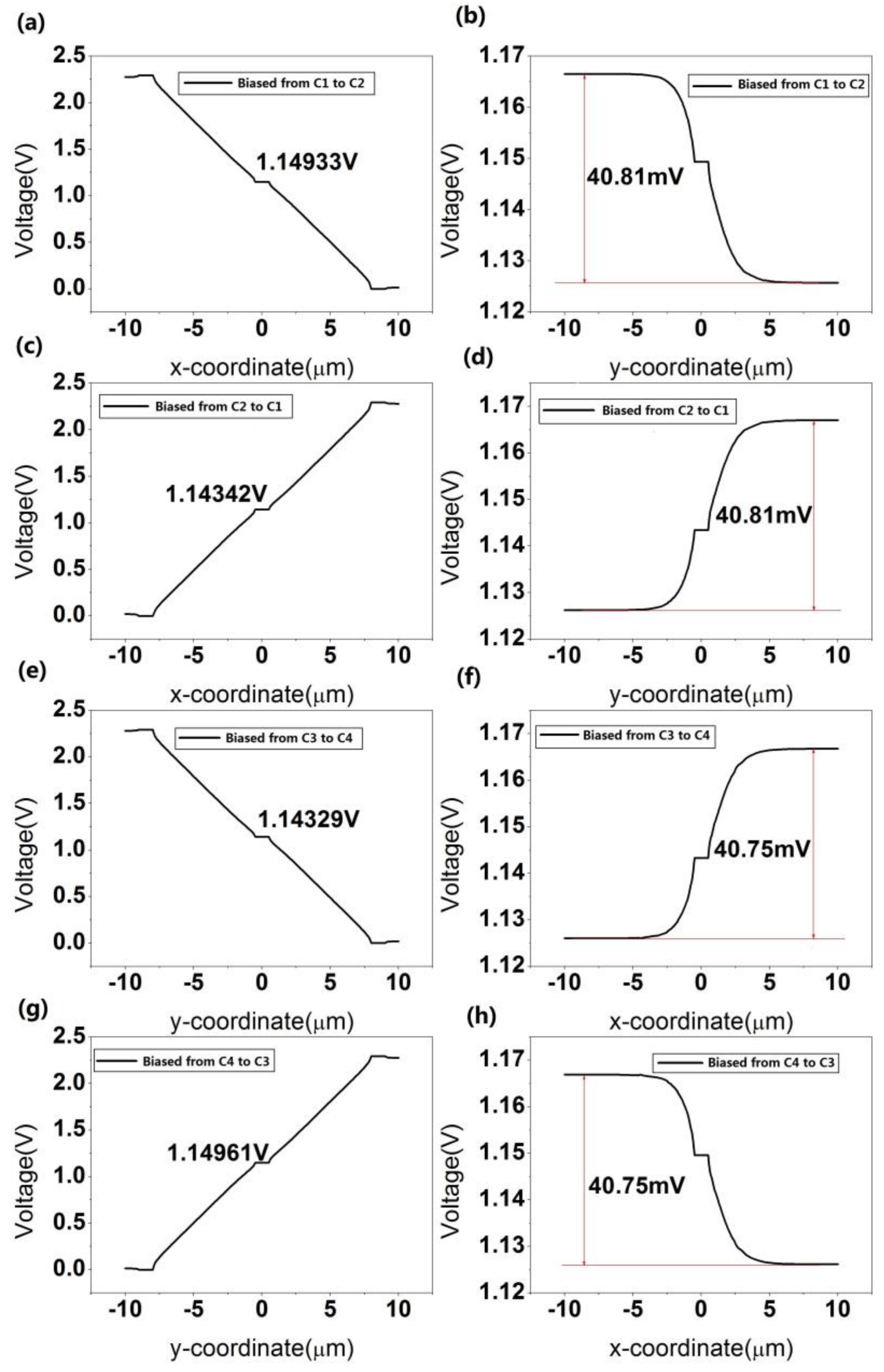
For details of the cross-shaped 3D Hall device, the magnetic field is set to 1T in all three directions. Figure 13 shows the simulation results of the cross-shaped 3D Hall device under different biases and directions. It can be calculated that the current-related sensitivity in the x direction is 5.91 V/AT and the sensitivity in the y direction is 6.32 V/AT. When the biasing current is applied from C1 to C2 or C2 to C1, the SI in the z direction is 40.81 V/AT. The sensitivity can reach up to 40.75 V/AT if the bias is from C3 to C4 or C4 to C3.
There are some differences between the components of the sensitivities in the x and y directions. When the cross-shaped 3D Hall device is used as a horizontal device, there remain some differences in the sensitivities of the z direction under different biases. This is because COMSOL solves a complex problem by dividing it into smaller, simpler parts. The software uses the “Mesh” function to define the amount and size of the domain and boundary elements. During the simulation, a “Free Triangular Mesh” (simpler part) is selected. This method results in the components of the cross-shaped 3D Hall device in the x and y directions being not identical as well as in the small discrepancies in the sensitivities.
Furthermore, the sensitivity of the device in the z direction is much better than those in the x and y directions when the active region is 1.018 μm. This originates from the different demands for the depth of the active region in the three directions. The shallow depth limits the flow of current, but increases the Hall voltage of the z direction. To overcome this difficulty, a CMOS technology with an additional deep n-well is compatible with the requirements for high sensitivities in the x and y directions.
4. Improvement of the Cross-Shaped 3D Hall Device
The doping concentration and the depth of the active region can affect the behavior of the Hall sensors. Reducing the doping concentration of the active region can result in a promotion of the current-related sensitivity of the Hall sensors, mainly due to the increase of the Hall coefficient. In this section, the doping concentration is lower than the one in the standard process and dramatically enhances the sensitivities. The conventional Hall device requires a shallow depth of the active region, which is beneficial to reducing the thickness along the magnetic field and promoting the increase of the Hall voltage and sensitivities. The vertical Hall device, however, requires a deep active region for a high sensitivity. Therefore, consideration and analysis of the sensitivities in the horizontal (x and y) and vertical (z) directions are needed.
Figure 14 shows that the current-related sensitivity in the z direction is highly dependent on the depth of the active region and that the curve of sensitivity changing with the depth is similar to an inverse proportional function. In addition, sensitivities in the x and y directions show little difference, with both showing a similar slightly increasing tendency. These simulation results indicate that 5 μm is an optimized depth for balancing the performance in all directions. The sensitivities in the directions of x, y, and z are 76.19 V/AT, 71.50 V/AT, and 75.70 V/AT, respectively.
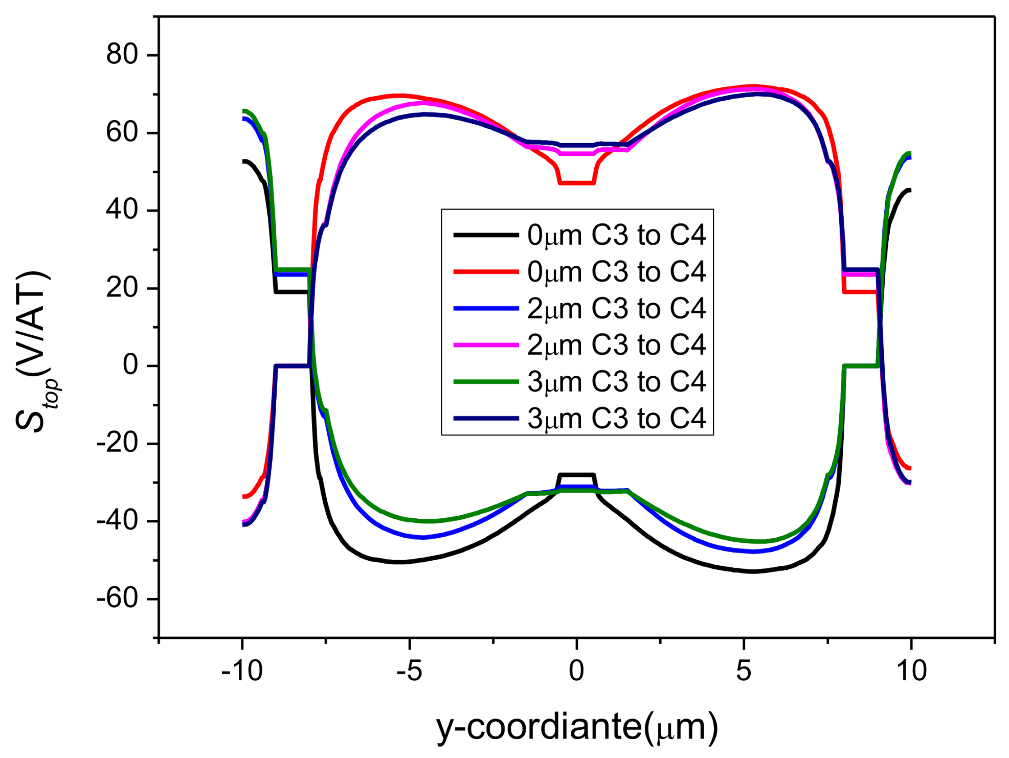
The effects of P-type layers with various thickness on the sensitivities of the cross-shaped 3D Hall device were also studied. The depth of the active region was set to 7 μm for a full investigation. Figure 15 shows the current-related sensitivities in the x, y, and z directions with respect to the depth of the P-type layers. Sensitivity in the z direction is affected obviously with the increase of the P-type layers’ thickness for degradation in the depth along Bz. The components of sensitivities in the x and y directions show a small increasing response to the change of P-type layers. Furthermore, the differences between the two components vary irregularly. The differences also originate from the simpler parts divided by the Mesh function. To gain a better sense of the P-type layers’ effects on the horizontal direction, we depicted the changing curve of Stop corresponding to the depth as shown in Figure 16. It is found from the comparison of Figure 9 and Figure 16 that the short-circuiting effect has faded since the active region is 7 μm. Despite the P-type layers, the behavior changes a little. The sensitivities balance when the depth of the P-type layers is 3 μm and reach up to 91.70 V/AT, 92.36 V/AT, and 87.10 V/AT in the directions of x, y, and z, respectively.
To provide a better comparison, we list some key prior works. Those works which focused on integrating horizontal and vertical Hall devices into the same chip have been excluded. Detailed information is displayed in Table 4. The sensitivities in the horizontal and vertical directions cannot be optimized simultaneously due to the opposite demands on the active region [13]. Though a balanced performance is achieved [14,15,16], there is a compromise in one of sensitivities in the horizontal and vertical directions. In our work, the sensitivities of x, y, and z can reach 91.70 V/AT, 92.36 V/AT, and 87.10V/AT by adjusting the depth of the active region and P-type layers, albeit in COMSOL. This can provide another method for the study of the single-device 3D Hall sensors.
5. Conclusions
In order to measure the magnetic field in three directions, we designed a new cross-shaped 3D Hall device by integrating two three-contact vertical Hall devices derived from the five-contact vertical Hall device. Some of the device’s parameters were based on 0.18 μm BCDliteTM technology provided by GLOBALFOUNDRIES. The behavior was studied through an analysis of FEM calculations. A fitting model in COMSOL can provide more chances for exploration and thus reduce the number of iterations and improve efficiency before manufacturing devices. To have detailed knowledge of the devices, the sensing contact and P-type layers were taken into account by analyzing the distribution of the voltage along the top edge and the current density. The P-type layers were demonstrated to be able to weaken the short-circuiting effect by keeping the behavior of the current under control. Meanwhile, adjusting the depth of the active region and the thickness of the P-type layer provides a way to balance the performance. When the depth of the active region and the thickness of the P-type layer are set to 7 μm and 3 μm, the sensitivities in the directions of x, y, and z are 91.70 V/AT, 92.36 V/AT, and 87.10 V/AT, respectively. In general, FEM provides an easy-to-use method for breaking down a complex problem into a simple one and for the preverification of the performance of devices.
Acknowledgments
This work was supported by National Nature Science Foundation of China under Grant No. 61376075; the Key Research and Development Program of Jiangsu Province under Grant No. BE2015153.
Author Contributions
Wei Tang wrote and revised the manuscript, and also designed the Hall devices. Fei Lyu helped design the devices and carried out the experiments. Dunhui Wang provided keen insight for this manuscript. Hongbing Pan arranged all the work in this project.
Conflicts of Interest
The authors declare no conflict of interest.
References
- Ramsden, E. Hall-Effect Sensor: Theory and Application; Elsevier: Philadelphia, PA, USA, 2011. [Google Scholar]
- Boero, G.; Demierre, M.; Popovic, R.S. Micro-Hall devices: Performance, technologies and applications. Sens. Actuators A Phys. 2003, 106, 314–320. [Google Scholar] [CrossRef]
- Lyu, F.; Liu, X.F.; Ding, X.F.; Toh, E.H.; Zhang, Z.Y.; Pan, Y.F.; Wang, Z.; Li, C.J.; Li, L.; Sha, J.; et al. Influences of an Aluminum Covering Layer on the Performance of Cross-Like Hall Devices. Sensors 2016, 16, 106. [Google Scholar] [CrossRef] [PubMed]
- Popovic, R.S. Hall Effect Devices; CRC Press: Boca Raton, FL, USA, 2003. [Google Scholar]
- Sileo, L.; Todaro, M.T.; Tasco, V.; De Vittorio, M.; Passaseo, A. Fully integrated three-axis hall magnetic sensor based on micromachined structures. Microelectron. Eng. 2010, 87, 1217–1219. [Google Scholar] [CrossRef]
- Wouters, C.; Vranković, V.; Rössler, C.; Sidorov, S.; Ensslin, K.; Wegscheider, W.; Hierold, C. Design and fabrication of an innovative three-axis hall sensor. Sens. Actuators A Phys. 2016, 237, 62–71. [Google Scholar] [CrossRef]
- Burger, F.; Besse, P.A.; Popovic, R.S. New fully integrated 3-d silicon hall sensor for precise angular-position measurements. Sens. Actuators A Phys. 1998, 67, 72–76. [Google Scholar] [CrossRef]
- Kejik, P.; Schurig, E.; Bergsma, F.; Popovic, R.S. First fully CMOS-integrated three-dimensional Hall probe. In Proceedings of the 13th International Conference on Solid-State Sensors, Actuators and Microsystems, 2005. Digest of Technical Papers (TRANSDUCERS’05), Seoul, Korea, 5–9 June 2005; pp. 317–320. [Google Scholar]
- Popovic, D.R.; Dimitrijevic, S.; Blagojevic, M.; Kejik, P.; Schurig, E.; Popovic, R.S. Three-axis teslameter with integrated hall probe free from the planar hall effect. In Proceedings of the IEEE Instrumentation and Measurement Technology Conference 2006 (IMTC 2006), Sorrento, Italy, 24–27 April 2006; pp. 1812–1815. [Google Scholar]
- Popovic, D.R.; Dimitrijevic, S.; Blagojevic, M.; Kejik, P.; Schurig, E.; Popovic, R.S. Three-axis teslameter with integrated Hall probe. IEEE Trans. Instrum. Meas. 2007, 56, 1396–1402. [Google Scholar] [CrossRef]
- Pascal, J.; Hebrard, L.; Frick, V.; Blonde, J.P. Three-dimensional Hall probe integrated in 0.35 μm CMOS technology for magnetic field pulses measurements. In Proceedings of the 2008 Joint 6th International IEEE Northeast Workshop on Circuits and Systems and TAISA Conference (NEWCAS-TAISA 2008), Montreal, QC, Canada, 22–25 June 2008; pp. 97–100. [Google Scholar]
- Schell, J.B.; Kammerer, J.B.; Hébrard, L.; Breton, E.; Gounot, D.; Guvillon, L.; de Mathelin, M. CMOS three-dimensional Hall probe for magnetic field measurement in MRI scanner. In Proceedings of the 2012 IEEE 10th International New Circuits and Systems Conference (NEWCAS), Montreal, QC, Canada, 17–20 June 2012; pp. 517–520. [Google Scholar]
- Roumenin, C.S.; Nikolov, D.I. Five-contact silicon structure based integrated 3D Hall sensor. Electron. Lett. 2003, 39, 1416–1424. [Google Scholar] [CrossRef]
- Lozanova, S.; Noykov, S.; Roumenin, C. A novel 3-D Hall magnetometer using subsequent measurement method. Sens. Actuators A Phys. 2009, 53, 205–211. [Google Scholar] [CrossRef]
- Sander, C.; Leube, C.; Aftab, T.; Ruther, P. Isotropic 3D silicon hall sensor. In Proceedings of the 28th IEEE International Conference on MICRO Electro Mechanical Systems (MEMS), Estoril, Portuga, 18–22 January 2015; pp. 893–896. [Google Scholar]
- Sander, C.; Leube, C.; Aftab, T.; Ruther, P.; Paul, O. Monolithic isotropic 3d silicon hall sensor. Sens. Actuators A Phys. 2016, 247, 587–597. [Google Scholar] [CrossRef]
- Frem, L.A. Hall Effect Modeling in FEM Simulators and Comparison to Experimental Results in Silicon and Printed Sensors. Master’s Thesis, California Polytechnic State University, San Luis Obispo, CA, USA, June 2016. [Google Scholar]
- Sun, J.; Kosel, J. Finite-element modelling and analysis of hall effect and extraordinary magnetoresistance effect. Mech. Eng. 2012, 119. [Google Scholar] [CrossRef]
- Ruskova, I.N.; Gieva, E.E.; Yantchev, V.M.; Hristov, M.H. COMSOL modeling of Hall sensors efficiency. In Proceedings of the XXVI International Scientific Conference Electronics(ET), Sozopol, Bulgaria, 13–15 September 2017; pp. 1–4. [Google Scholar]
- Heidari, H.; Bonizzoni, E.; Gatti, U.; Maloberti, F. A cmos current-mode magnetic hall sensor with integrated front-end. IEEE Trans. Circuits Syst. I Regul. Pap. 2015, 62, 1270–1278. [Google Scholar] [CrossRef]
- Heidari, H.; Bonizzoni, E.; Gatti, U.; Maloberti, F.; Dahiya, R. Cmos vertical hall magnetic sensors on flexible substrate. IEEE Sens. J. 2016, 16, 8736–8743. [Google Scholar] [CrossRef]
- Popovic, R.S. The vertical hall-effect device. IEEE Electron Device Lett. 2005, 5, 357–358. [Google Scholar] [CrossRef]
- Osberger, L.; Frick, V.; Hébrard, L. High resolution shallow vertical hall sensor operated with four-phase bi-current spinning current. Sens. Actuators A Phys. 2016, 244, 270–276. [Google Scholar] [CrossRef]
- Heidari, H.; Bonizzoni, E.; Gatti, U.; Maloberti, F. Analysis and modeling of four-folded vertical Hall devices in current domain. In Proceedings of the 10th Conference on Ph.D. Research in Microelectronics and Electronics (PRIME), Grenoble, France, 30 June–3 July 2014; pp. 1–4. [Google Scholar]
- Heidari, H.; Gatti, U.; Maloberti, F. Sensitivity characteristics of horizontal and vertical Hall sensors in the voltage-and current-mode. In Proceedings of the 11th Conference on Ph.D. Research in Microelectronics and Electronics (PRIME), Glasgow, UK, 29 June–2 July 2015; pp. 330–333. [Google Scholar]
- Sander, C.; Vecchi, M.C.; Cornils, M.; Paul, O. From three-contact vertical Hall elements to symmetrized vertical Hall sensors with low offset. Sens. Actuators A Phys. 2016, 240, 92–102. [Google Scholar] [CrossRef]
- Pascal, J.; Hébrard, L.; Frick, V.; Kammerer, J.B.; Blondé, J.P. Intrinsic limits of the sensitivity of cmos integrated vertical hall devices. Sens. Actuators A Phys. 2009, 152, 21–28. [Google Scholar] [CrossRef]
Figure 1.
A shift from five-contact to three-contact vertical Hall device. The light-green areas represent the active regions and the yellow ones represent the contacts.
Figure 1.
A shift from five-contact to three-contact vertical Hall device. The light-green areas represent the active regions and the yellow ones represent the contacts.
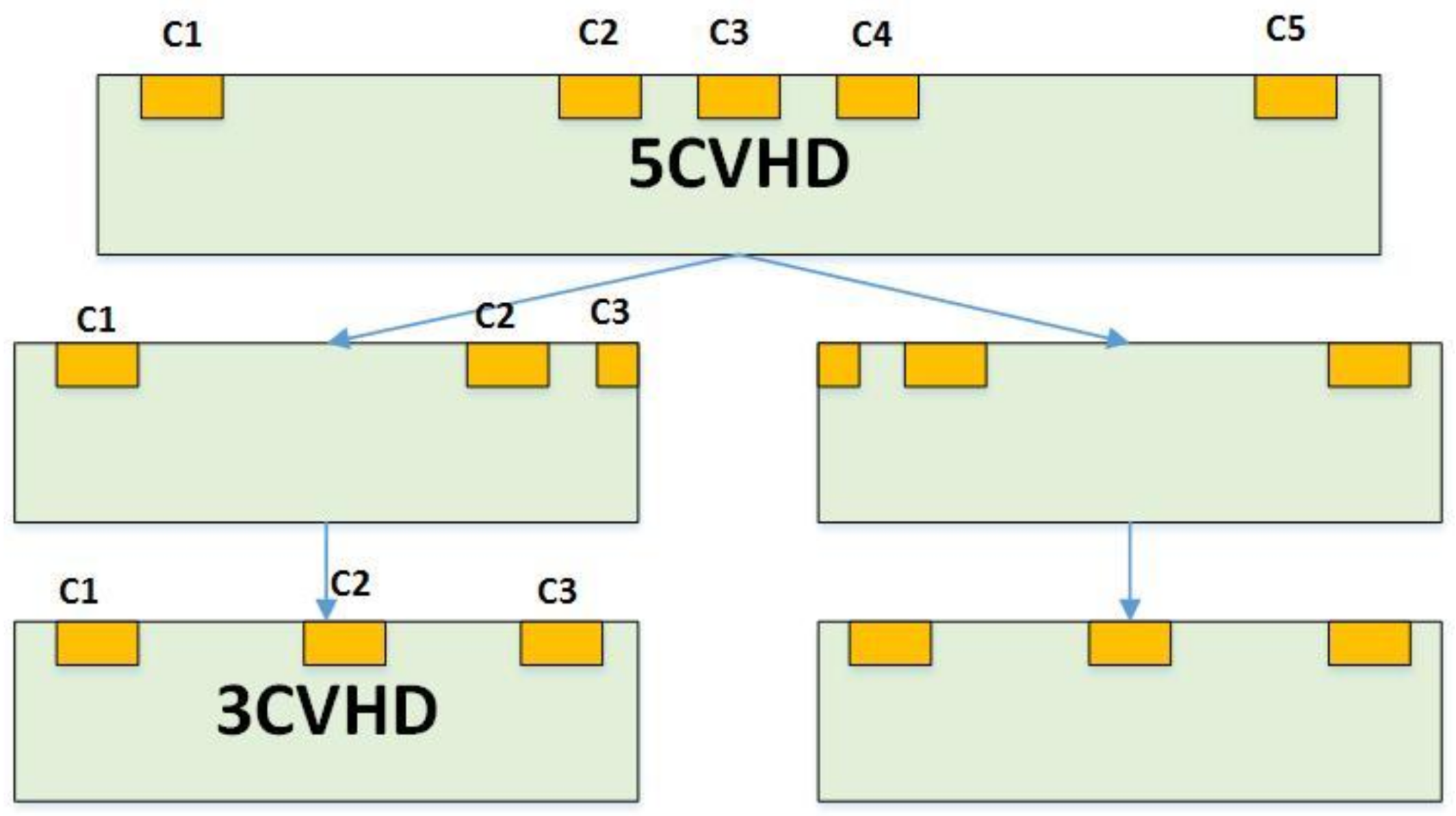
Figure 2.
(a) Three-contact vertical Hall device without sensing contact. (b) Three-contact vertical Hall device with sensing contact and (c) three-contact vertical Hall device with sensing contact and P-type layers.
Figure 2.
(a) Three-contact vertical Hall device without sensing contact. (b) Three-contact vertical Hall device with sensing contact and (c) three-contact vertical Hall device with sensing contact and P-type layers.

Figure 3.
(a) Voltage along the top edge of the three-contact vertical Hall device without C2 and (b) distribution of voltage around the middle of the device under different biases.
Figure 3.
(a) Voltage along the top edge of the three-contact vertical Hall device without C2 and (b) distribution of voltage around the middle of the device under different biases.
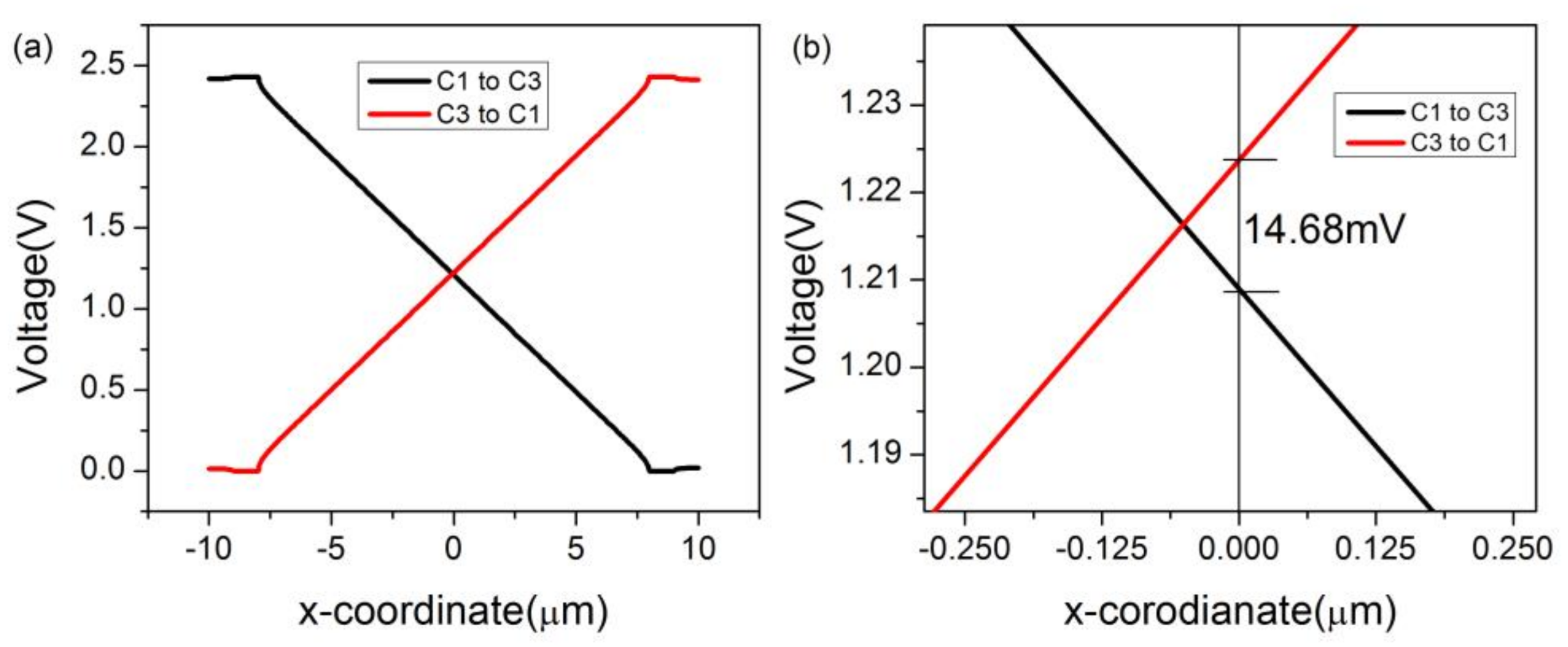
Figure 4.
(a) Voltage along the top edge of the three-contact vertical Hall device with C2 and (b) distribution of voltage around C2 under different biases.
Figure 4.
(a) Voltage along the top edge of the three-contact vertical Hall device with C2 and (b) distribution of voltage around C2 under different biases.
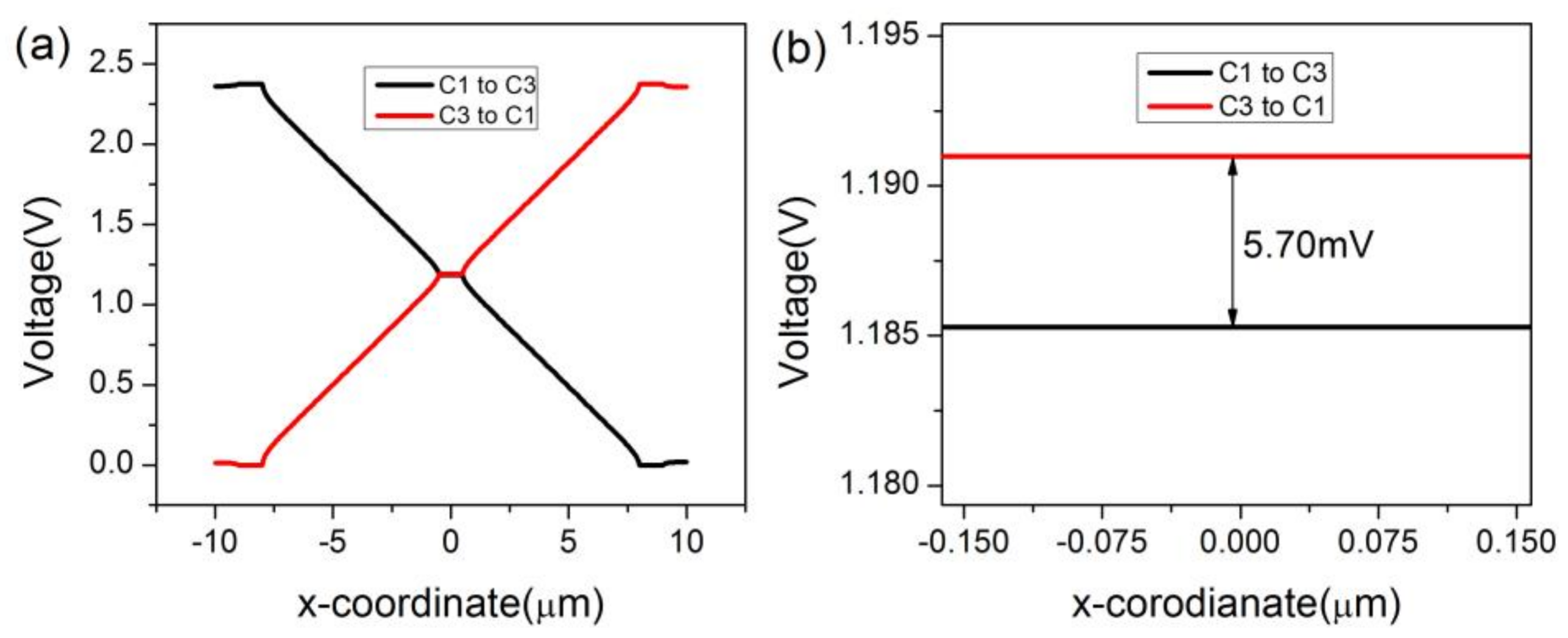
Figure 5.
(a) Voltage along the top edge of the three-contact vertical Hall device with C2 and P-type layers and (b) distribution of voltage around C2 under different biases.
Figure 5.
(a) Voltage along the top edge of the three-contact vertical Hall device with C2 and P-type layers and (b) distribution of voltage around C2 under different biases.

Figure 6.
Effects of sensing contact and P-type layers on Stop. SC represents the sensing contact and P represents the P-type layers.
Figure 6.
Effects of sensing contact and P-type layers on Stop. SC represents the sensing contact and P represents the P-type layers.
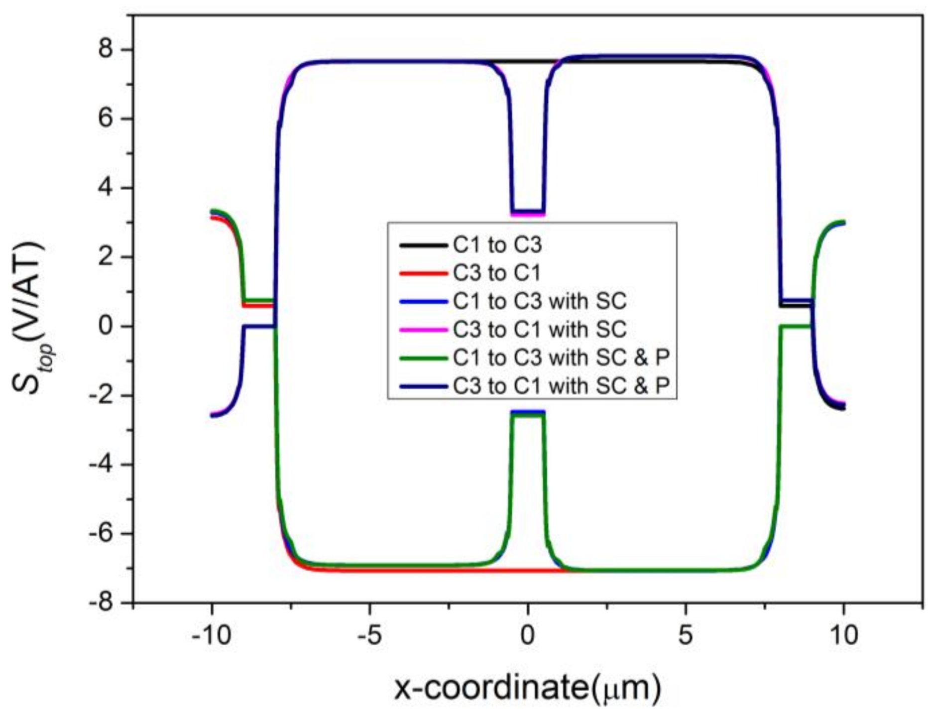
Figure 7.
Effects of sensing contact and P-type layers on distribution of current density. (a) Sensor without C2. (b) Sensor with C2. (c) Sensor with C2 and P-type layers and (d) comparisons between three structures. The device is 1.018 μm deep and P-type layers are 0.133 μm deep.
Figure 7.
Effects of sensing contact and P-type layers on distribution of current density. (a) Sensor without C2. (b) Sensor with C2. (c) Sensor with C2 and P-type layers and (d) comparisons between three structures. The device is 1.018 μm deep and P-type layers are 0.133 μm deep.
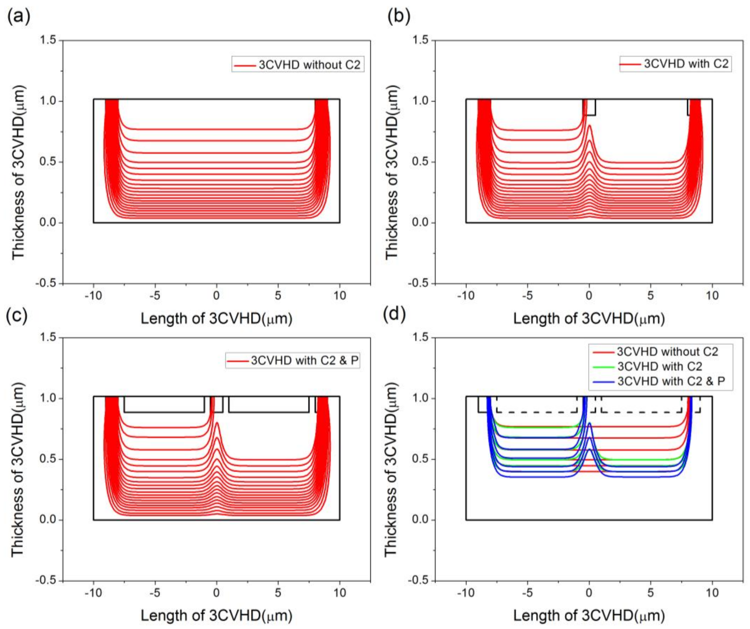
Figure 8.
Comparisons in the distribution of current density. (a) Sensor with C2. (b) Sensor with C2 and P-type layers. The device is 3 μm deep and P-type layers are 1 μm deep.
Figure 8.
Comparisons in the distribution of current density. (a) Sensor with C2. (b) Sensor with C2 and P-type layers. The device is 3 μm deep and P-type layers are 1 μm deep.
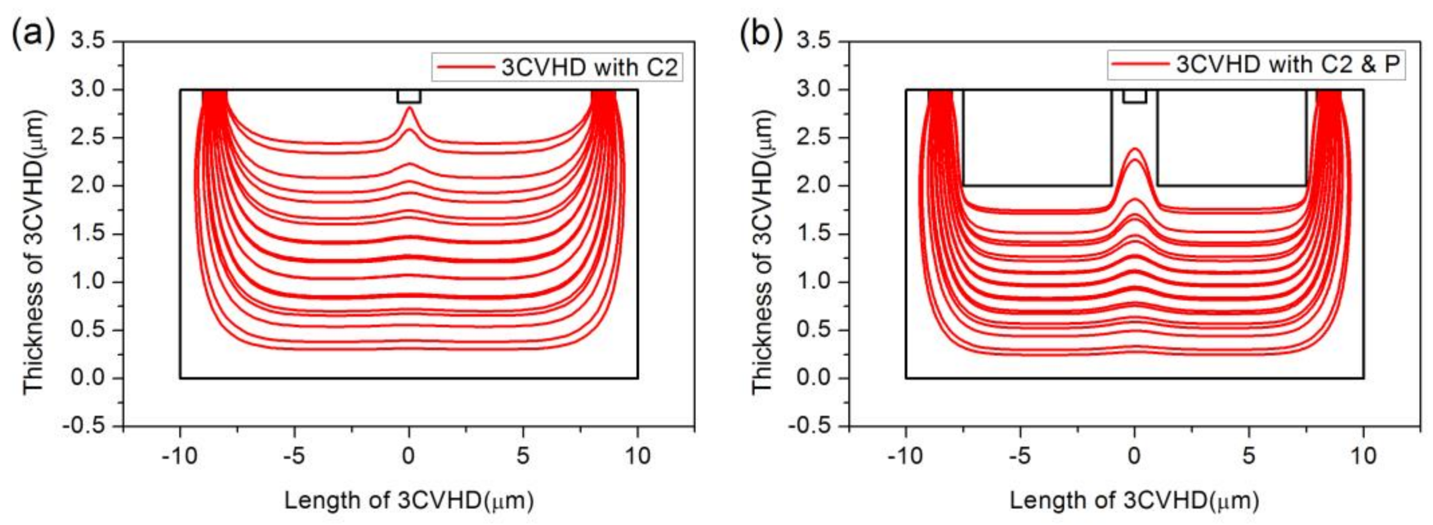
Figure 9.
Comparisons between different depths of the active region in Stop. The depth changes from 1 μm to 7 μm.
Figure 9.
Comparisons between different depths of the active region in Stop. The depth changes from 1 μm to 7 μm.
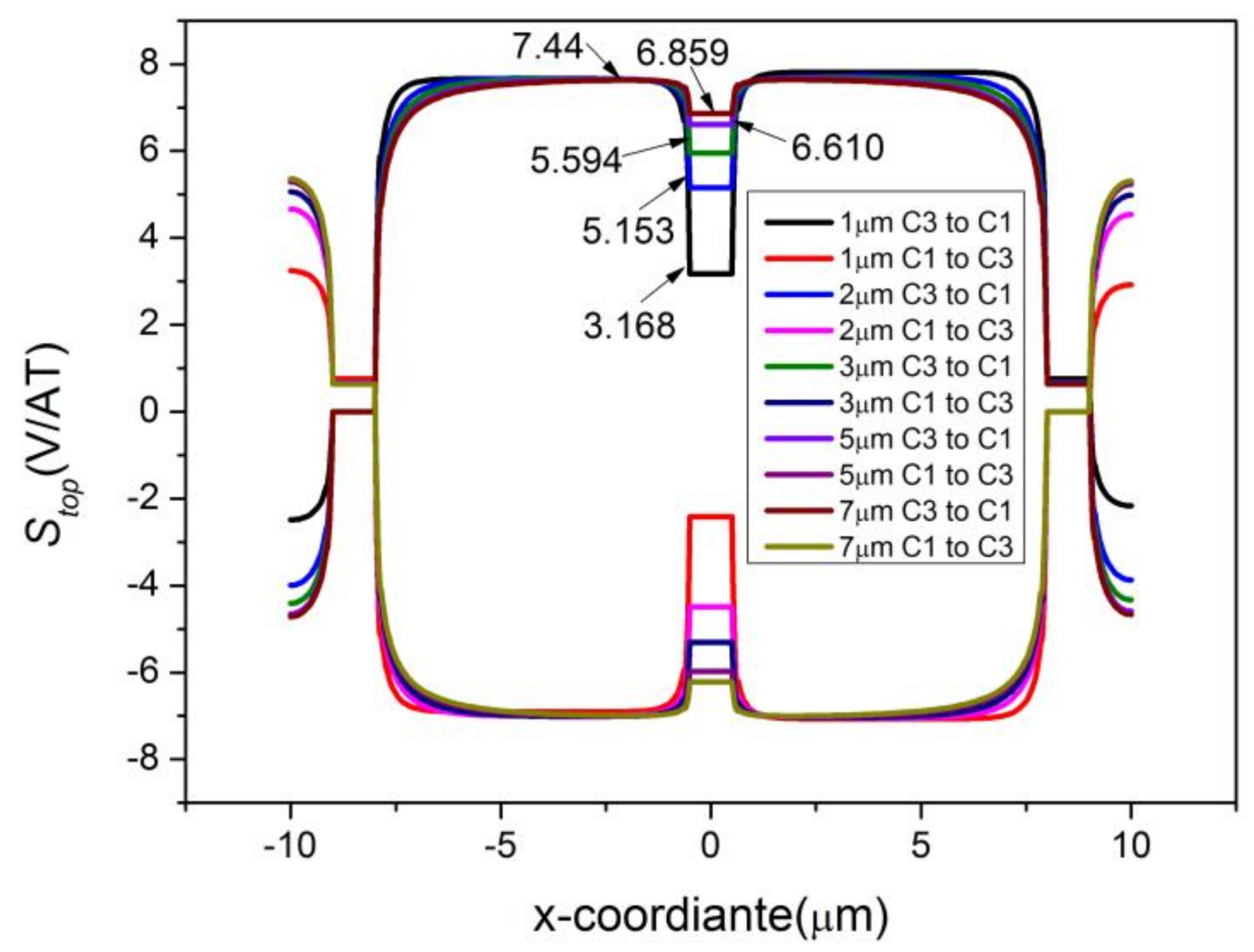
Figure 10.
Diagram of the cross-shaped 3D Hall device. Two orthogonal three-contact vertical Hall devices are placed in a cross shape.
Figure 10.
Diagram of the cross-shaped 3D Hall device. Two orthogonal three-contact vertical Hall devices are placed in a cross shape.
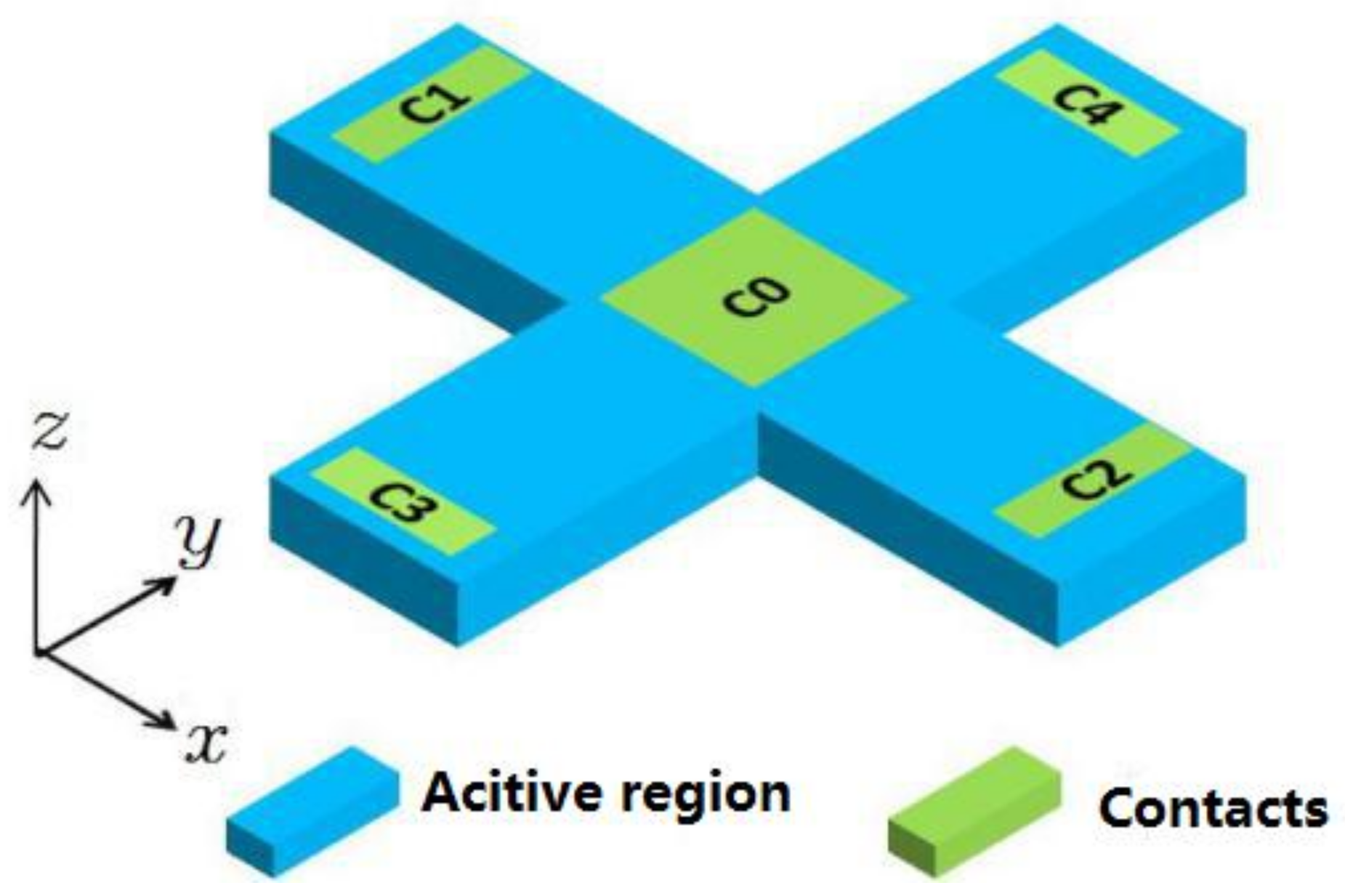
Figure 11.
Voltage distribution of the horizontal and cross-shaped 3D Hall devices in 3D space and in the x, y plane. (a,b) Horizontal Hall device. (c,d) Cross-shaped 3D Hall device.
Figure 11.
Voltage distribution of the horizontal and cross-shaped 3D Hall devices in 3D space and in the x, y plane. (a,b) Horizontal Hall device. (c,d) Cross-shaped 3D Hall device.
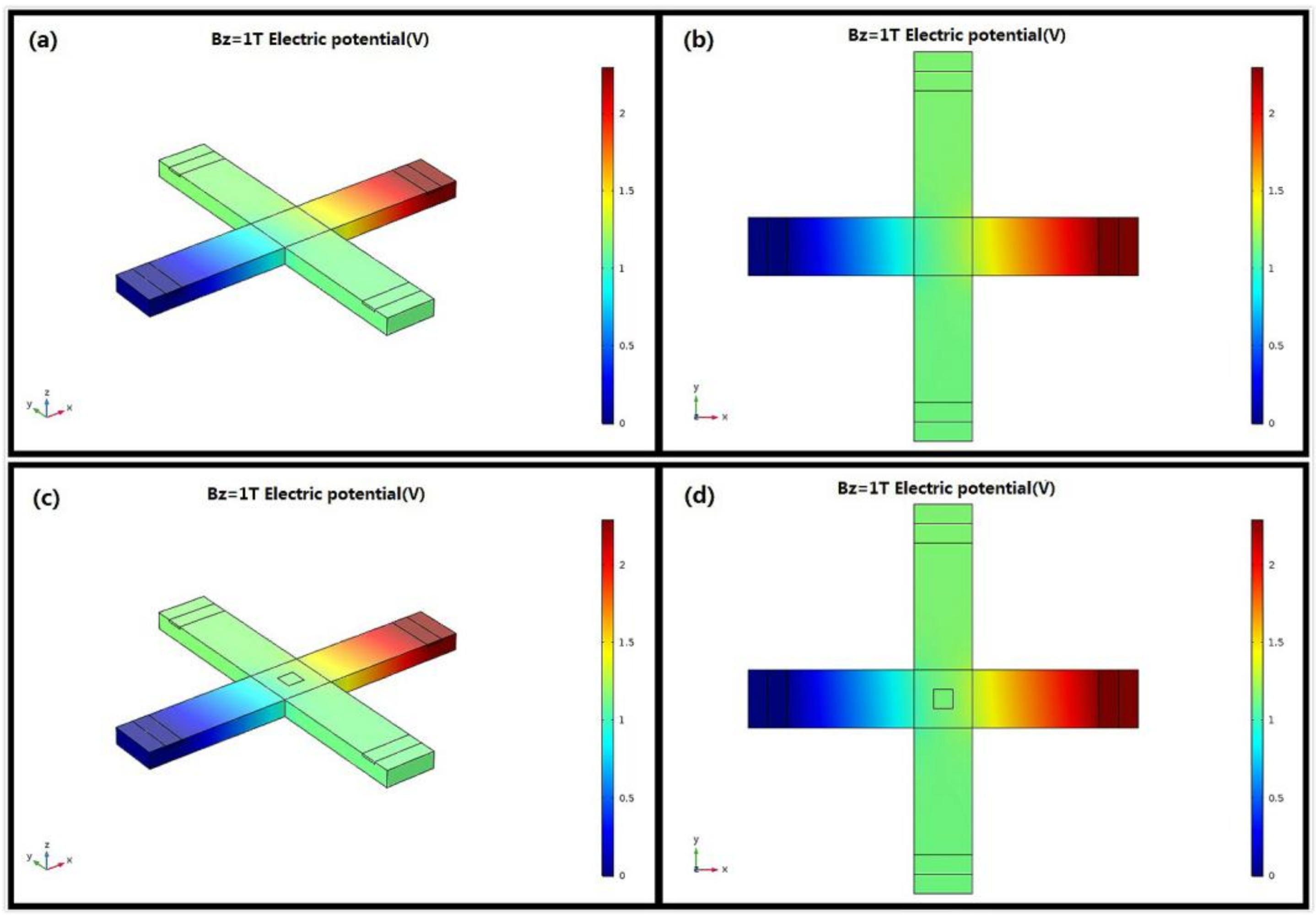
Figure 12.
Effects of sensing contact on the distribution of voltage in x and y directions. (a) Horizontal Hall device and (b) cross-shaped 3D Hall device.
Figure 12.
Effects of sensing contact on the distribution of voltage in x and y directions. (a) Horizontal Hall device and (b) cross-shaped 3D Hall device.
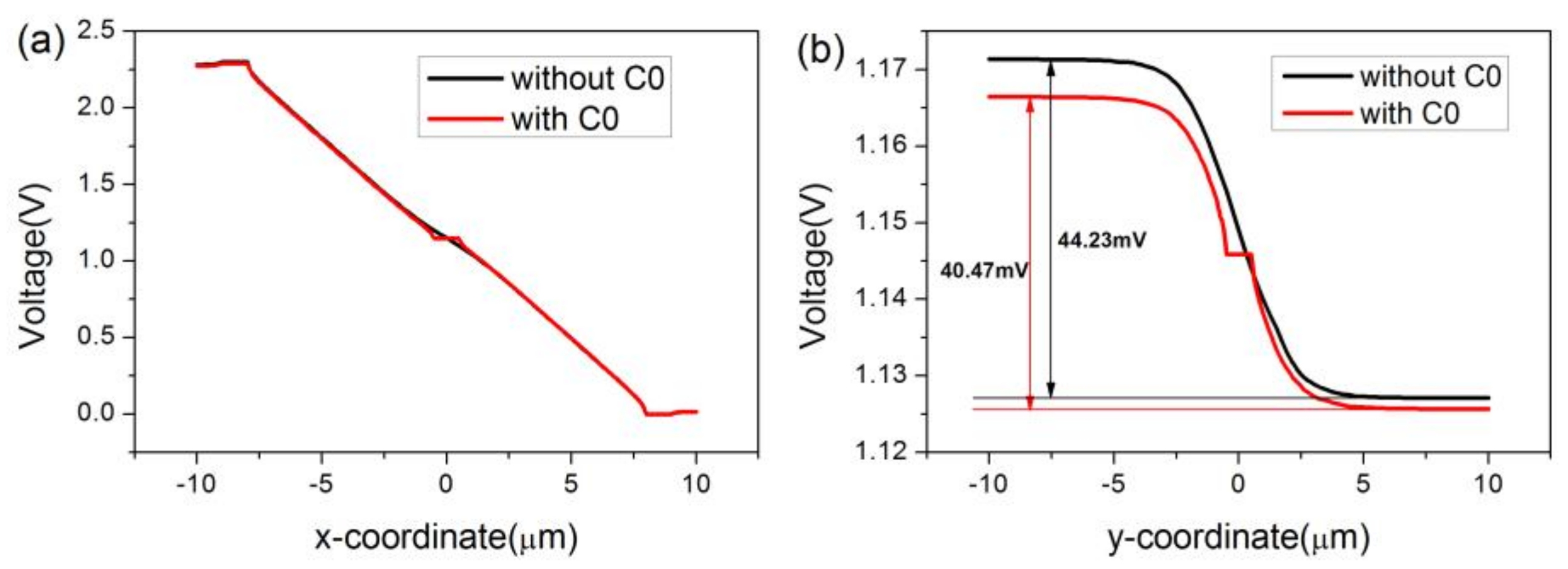
Figure 13.
Simulation for cross-shaped 3D Hall device under different biases. (a,b) Distribution of voltage in x and y directions when biased from C1 to C2, respectively. (c,d) Distribution of voltage in x and y directions when biased from C2 to C1, respectively. (e,f) Distribution of voltage in y and x directions when biased from C3 to C4, respectively. (g,h) Distribution of voltage in y and x directions when biased from C4 to C3, respectively.

Figure 14.
Relationships between the current-related sensitivities in three directions and the active region’s depth. The depth changes from 1 μm to 7 μm.
Figure 14.
Relationships between the current-related sensitivities in three directions and the active region’s depth. The depth changes from 1 μm to 7 μm.
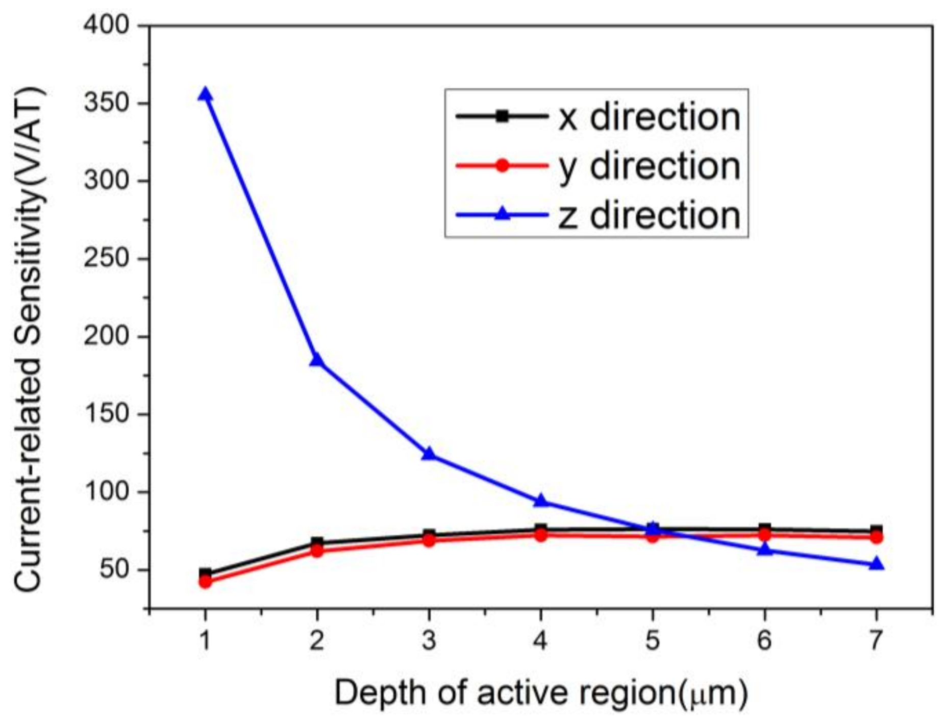
Figure 15.
Relationships between the current-related sensitivities in three directions and the P-type layers’ depth. The depth of the active region is 7 μm.
Figure 15.
Relationships between the current-related sensitivities in three directions and the P-type layers’ depth. The depth of the active region is 7 μm.
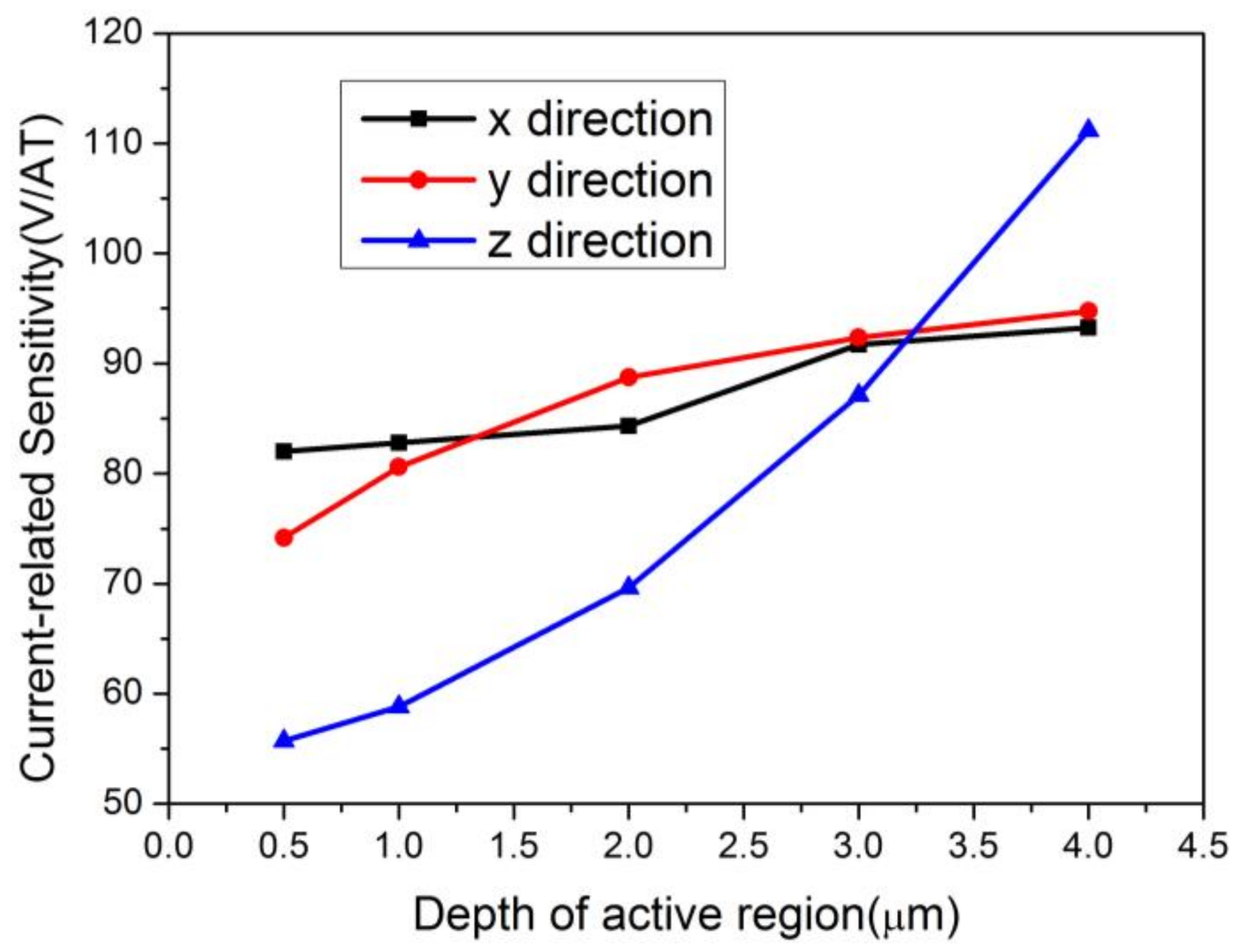
Figure 16.
Comparisons between different depths of P-type layers in Stop. The cross-shaped 3D Hall device is 7 μm deep. ‘0 μm’ represents a device without P-type layers.
Figure 16.
Comparisons between different depths of P-type layers in Stop. The cross-shaped 3D Hall device is 7 μm deep. ‘0 μm’ represents a device without P-type layers.

Table 1.
Comparisons between five-contact and three-contact vertical Hall devices. The characteristics of the devices are physical symbols instead of detailed information. f represents the frequency of conversion of the biasing current.
Table 1.
Comparisons between five-contact and three-contact vertical Hall devices. The characteristics of the devices are physical symbols instead of detailed information. f represents the frequency of conversion of the biasing current.
| Parameter | Five-Contact Vertical Hall Device | Three-Contact Vertical Hall Device |
|---|---|---|
| Length | l | l/2 |
| Width | w | w |
| Thickness | t | t |
| Biasing current | I | I |
| Power | P | 2P |
| Recognition rate | Real-time | 1/f |
Table 2.
Three-contact Hall device parameters and operating characteristics.
| Parameter | Symbol | Value | Unit |
|---|---|---|---|
| Sensor length | l | 20 | μm |
| Sensor width | w | 3 | μm |
| Sensor thickness | t | 1.018 | μm |
| Contact length | lc | 1 | μm |
| Contact width | wc | 3 | μm |
| Contact thickness | tc | 0.133 | μm |
| P-type layer thickness | tp | 0.133 | μm |
| Biasing current | I | 1 | mA |
Table 3.
Cross-shaped 3D Hall device parameters and operating characteristics.
| Parameter | Symbol | Value | Unit |
|---|---|---|---|
| Sensor length | l | 20 | μm |
| Sensor width | w | 3 | μm |
| Sensor thickness | t | 1.018 | μm |
| C0/C1/C2/C3/C4 length | lc | 1 | μm |
| C1/C2/C3/C4 width | wc | 3 | μm |
| C0 width | wc0 | 1 | μm |
| C0/C1/C2/C3/C4 thickness | tc | 0.133 | μm |
| P-type layer thickness | tp | 0.133 | μm |
| Biasing current | I | 1 | mA |
Table 4.
Performances of the single-device 3D Hall sensors based on different technologies.
| Time | Technology | Sensitivity in Vertical Direction (V/AT) | Sensitivity in Horizontal Direction (V/AT) | Reference |
|---|---|---|---|---|
| 2003 | Silicon Technology, with Low Doped N–Si Substrate | 29 | 85 | [13] |
| 2009 | CMOS Technology | 36 | 27 | [14] |
| 2015 | Special Silicon Technology | 33.3 | 33/33.9 | [15,16] |
© 2018 by the authors. Licensee MDPI, Basel, Switzerland. This article is an open access article distributed under the terms and conditions of the Creative Commons Attribution (CC BY) license (http://creativecommons.org/licenses/by/4.0/).
Share and Cite
MDPI and ACS Style
Tang, W.; Lyu, F.; Wang, D.; Pan, H. A New Design of a Single-Device 3D Hall Sensor: Cross-Shaped 3D Hall Sensor. Sensors 2018, 18, 1065. https://doi.org/10.3390/s18041065
AMA Style
Tang W, Lyu F, Wang D, Pan H. A New Design of a Single-Device 3D Hall Sensor: Cross-Shaped 3D Hall Sensor. Sensors. 2018; 18(4):1065. https://doi.org/10.3390/s18041065
Chicago/Turabian StyleTang, Wei, Fei Lyu, Dunhui Wang, and Hongbing Pan. 2018. "A New Design of a Single-Device 3D Hall Sensor: Cross-Shaped 3D Hall Sensor" Sensors 18, no. 4: 1065. https://doi.org/10.3390/s18041065
Note that from the first issue of 2016, this journal uses article numbers instead of page numbers. See further details here.