
The Front-End Readout as an Encoder IC for Magneto-Resistive Linear Scale Sensors


Abstract
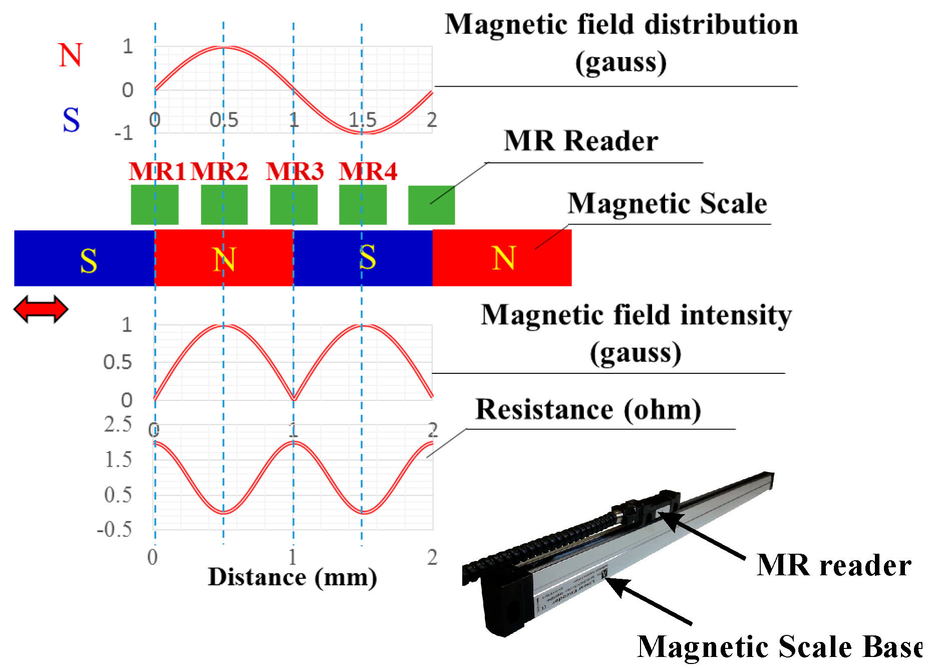
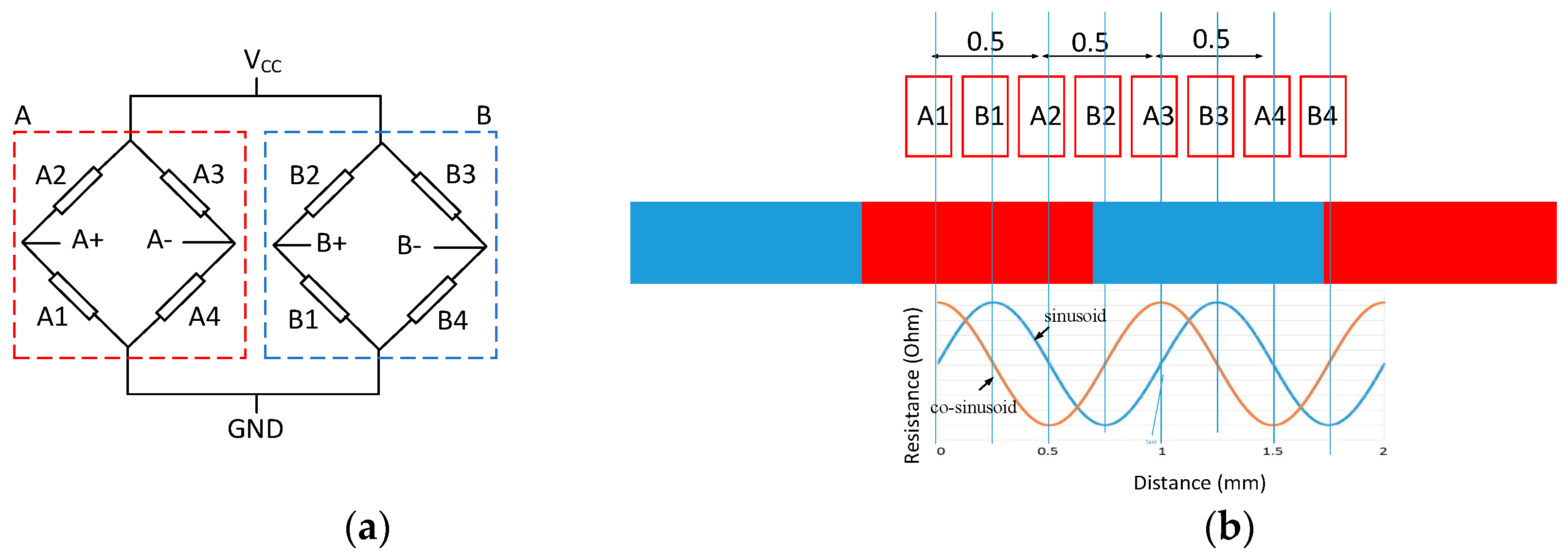
:1. Introduction
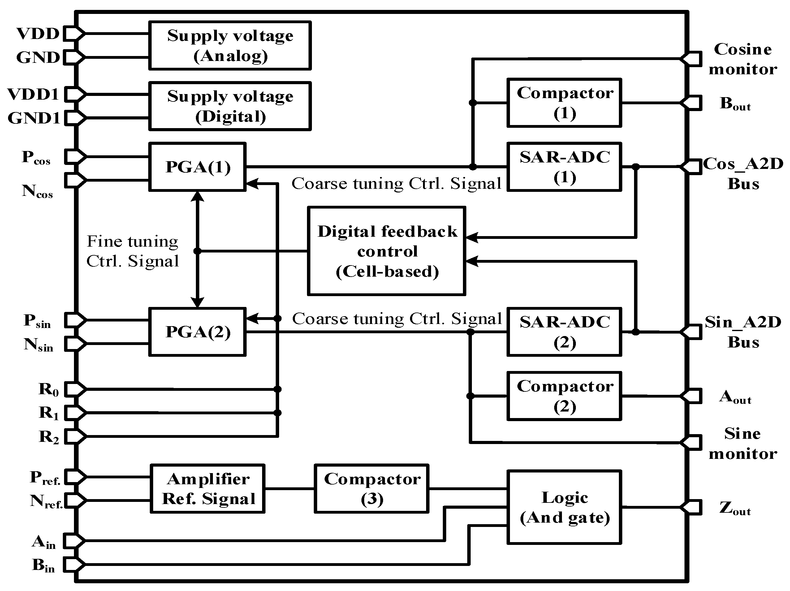
2. Chip Architecture Design
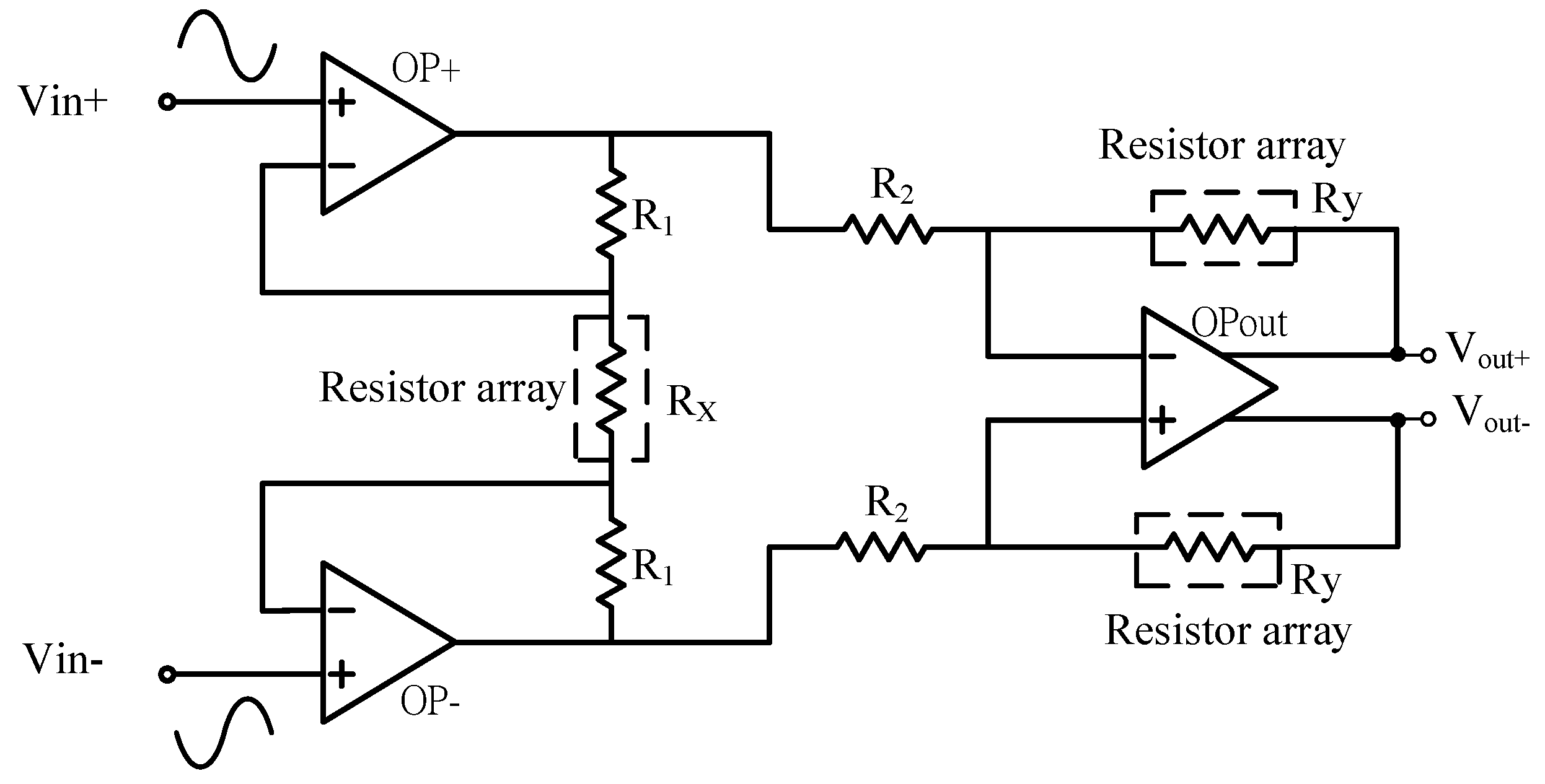
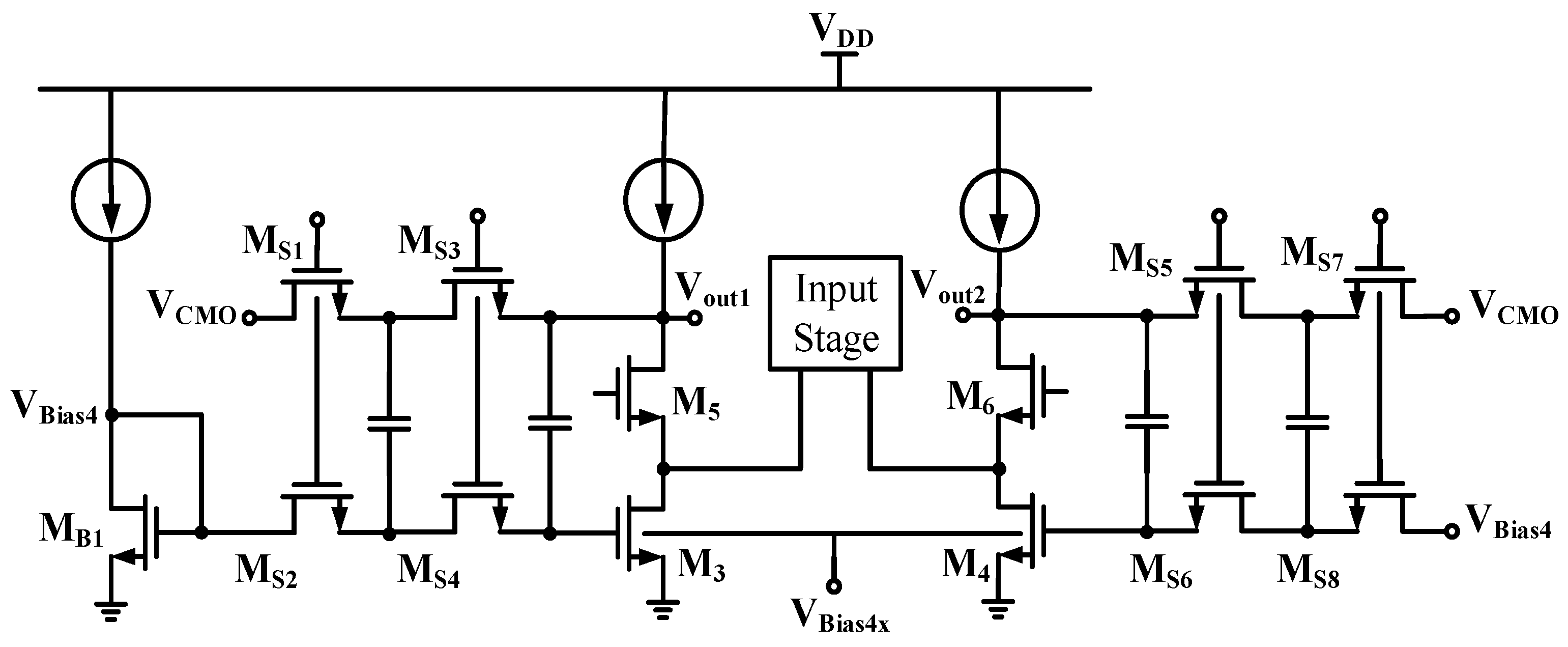
2.1. Programmable Gain Amplifier
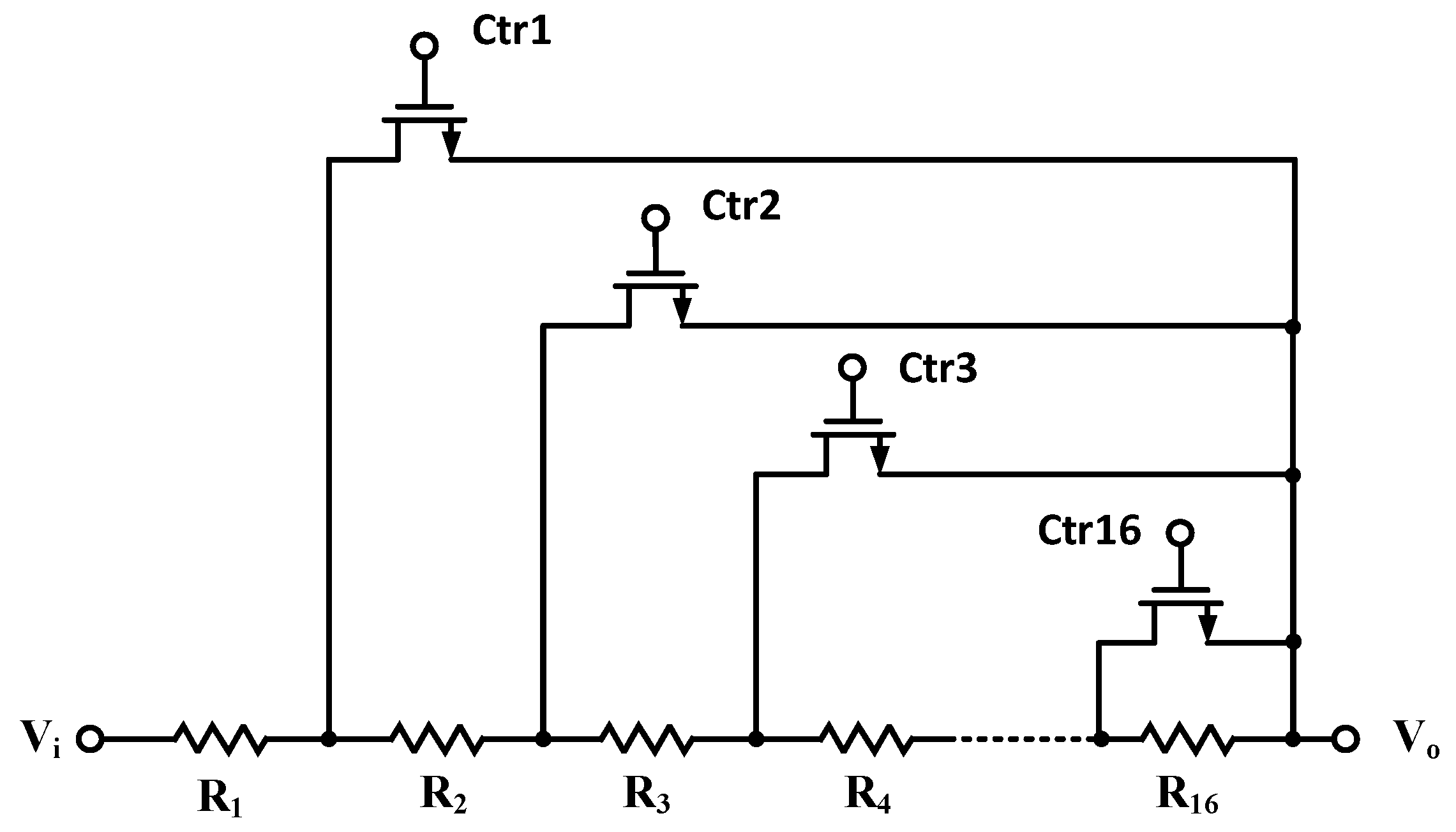
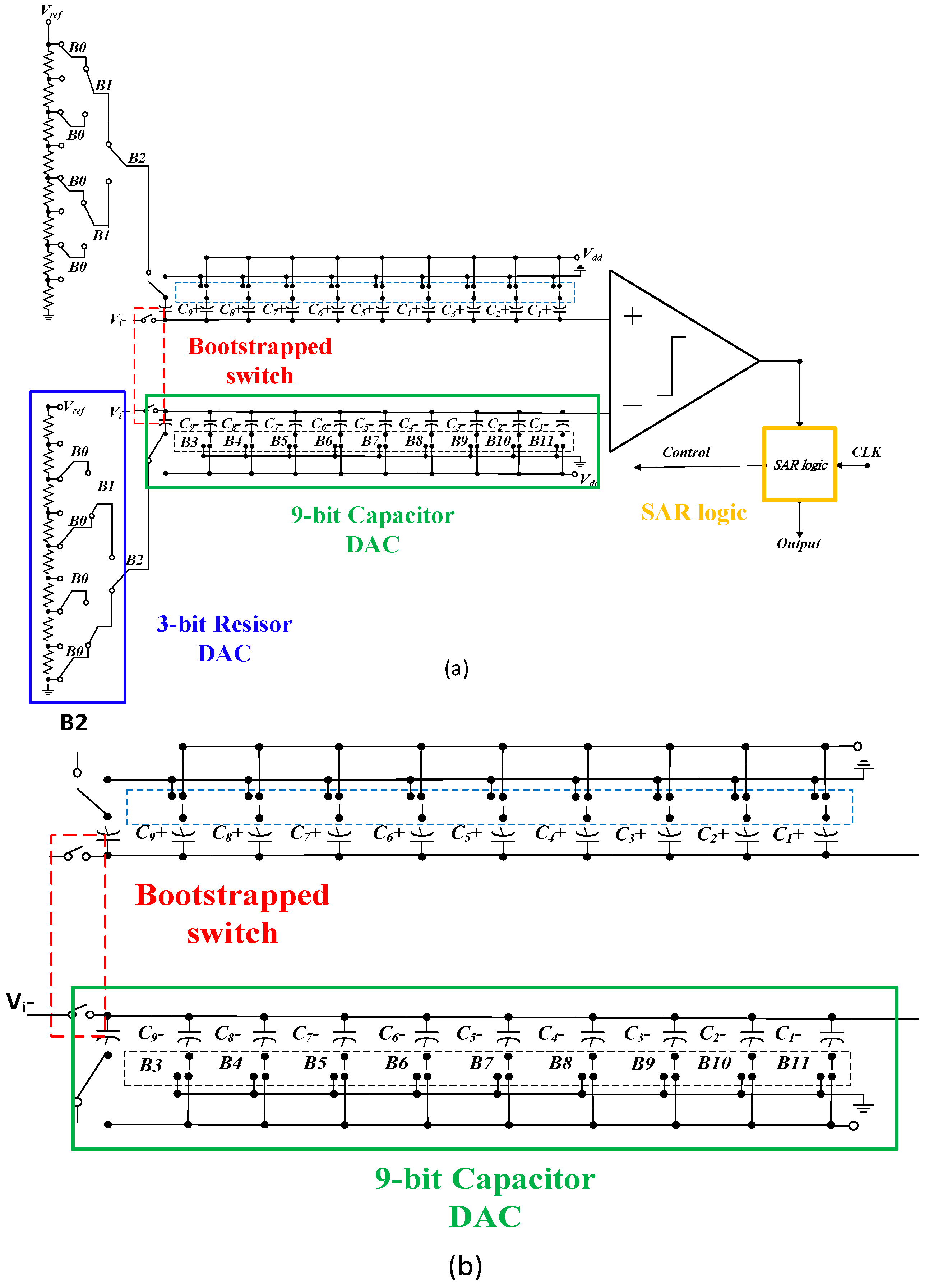
2.2. Switch Resistor Array and Decoder Block Circuit
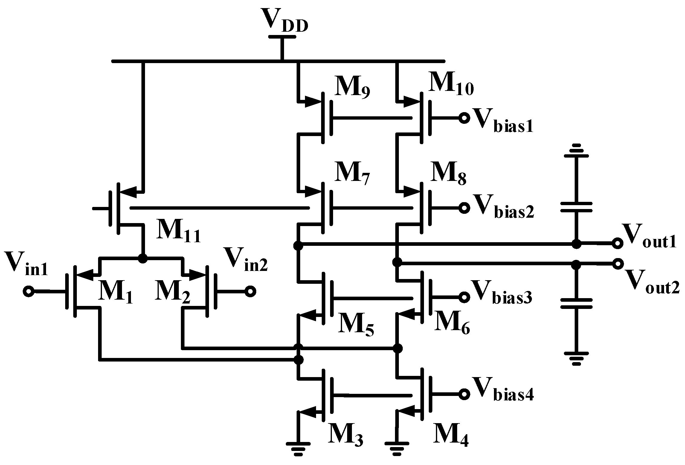
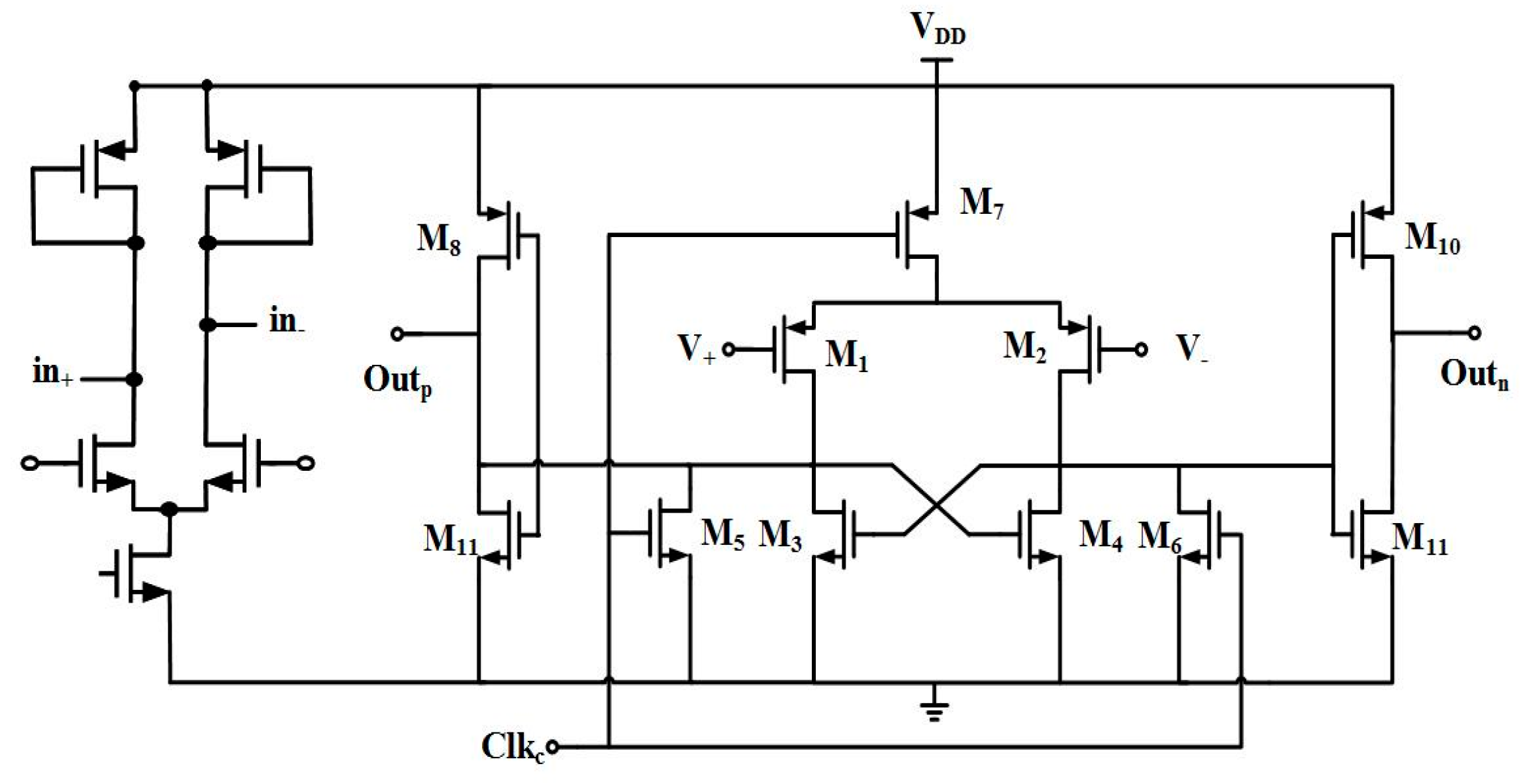
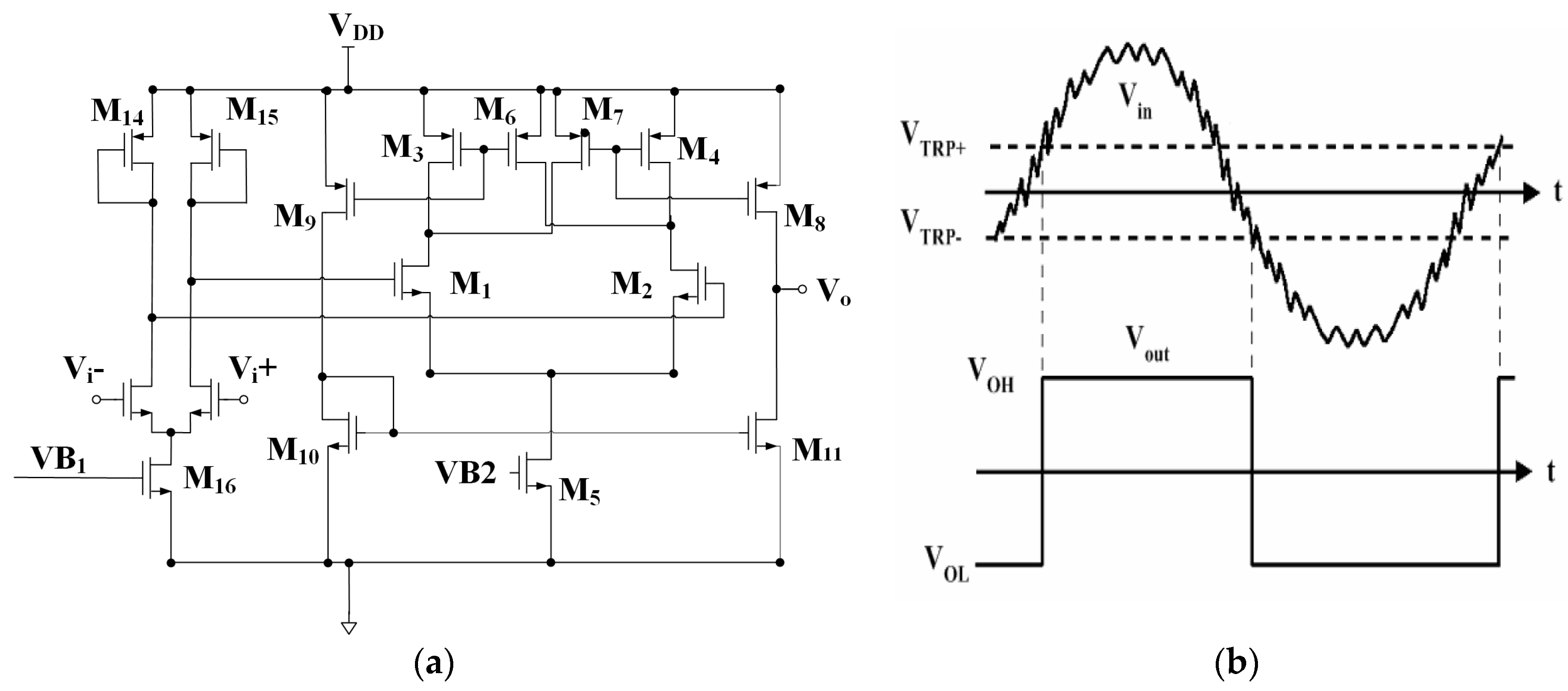
2.3. Hysteresis Comparator Design
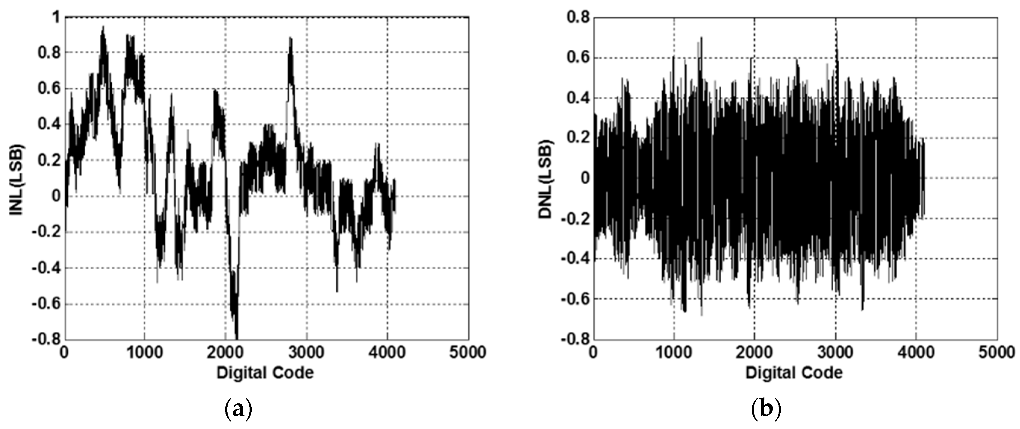
2.4. Successive Approximation Register ADC
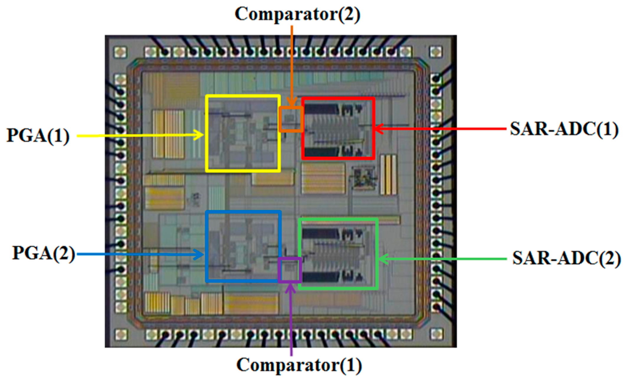
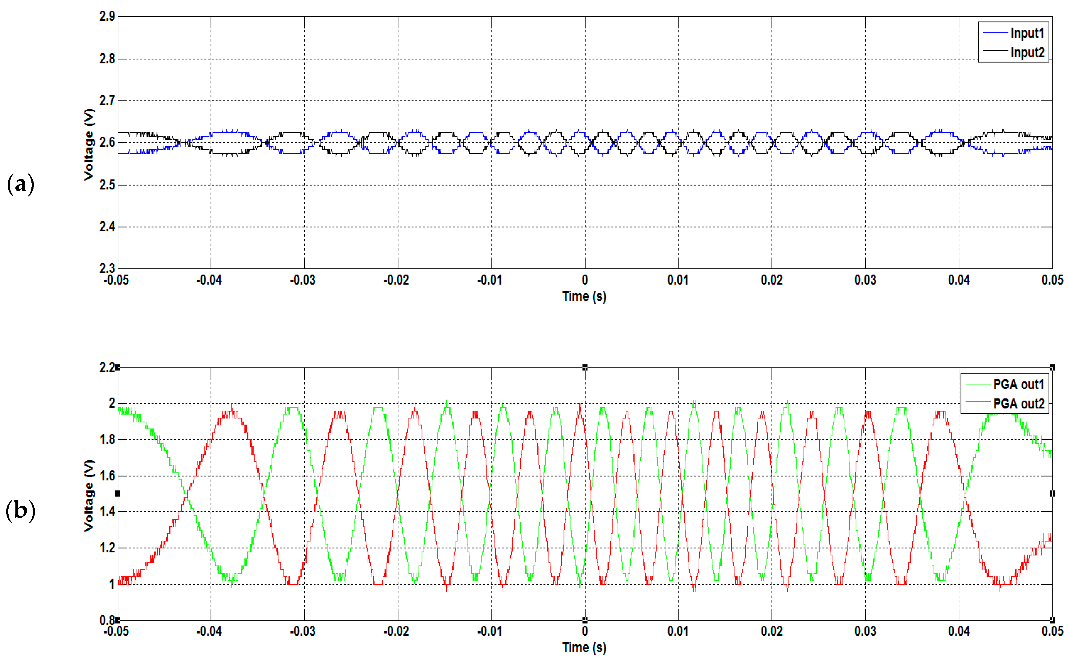
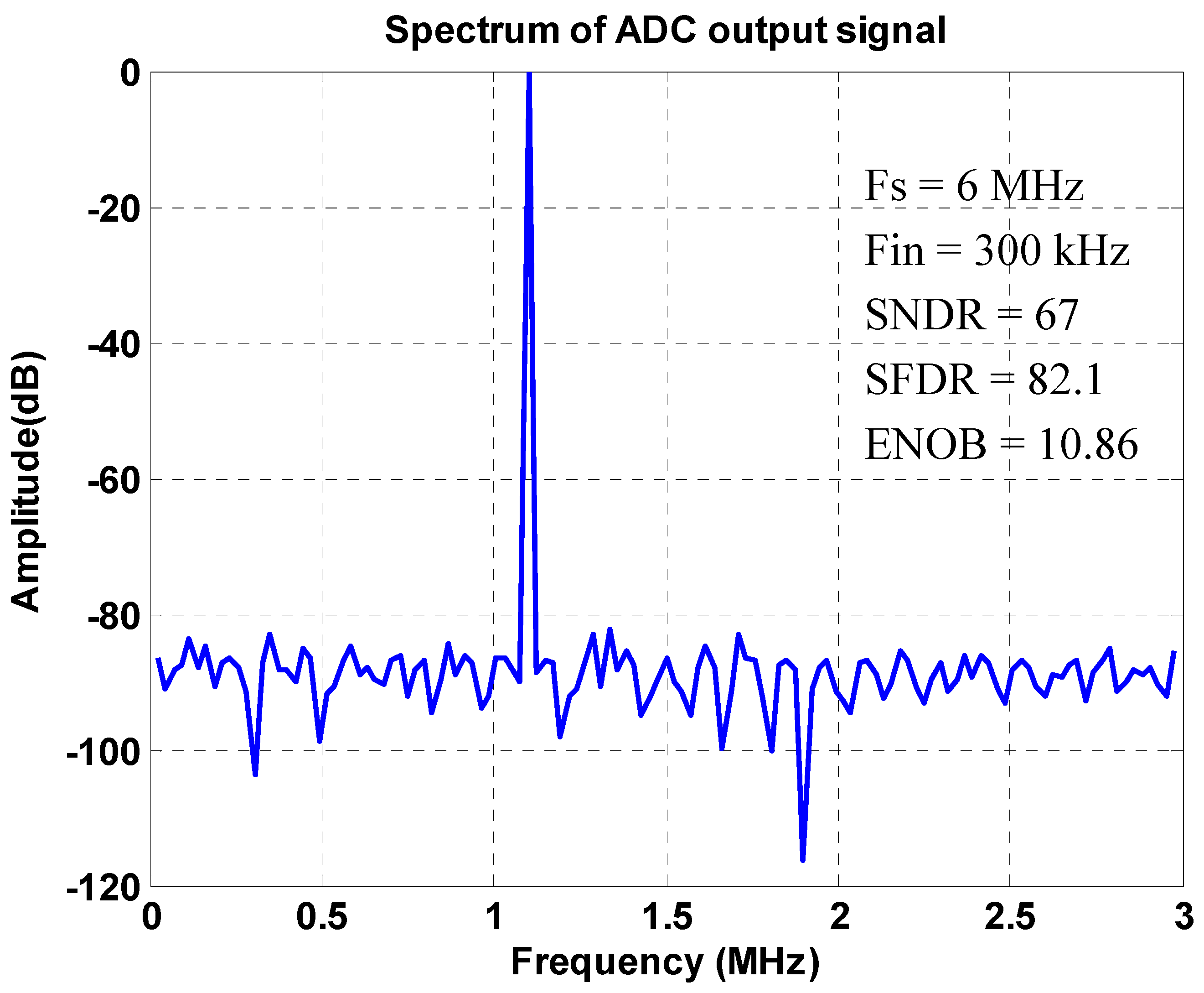
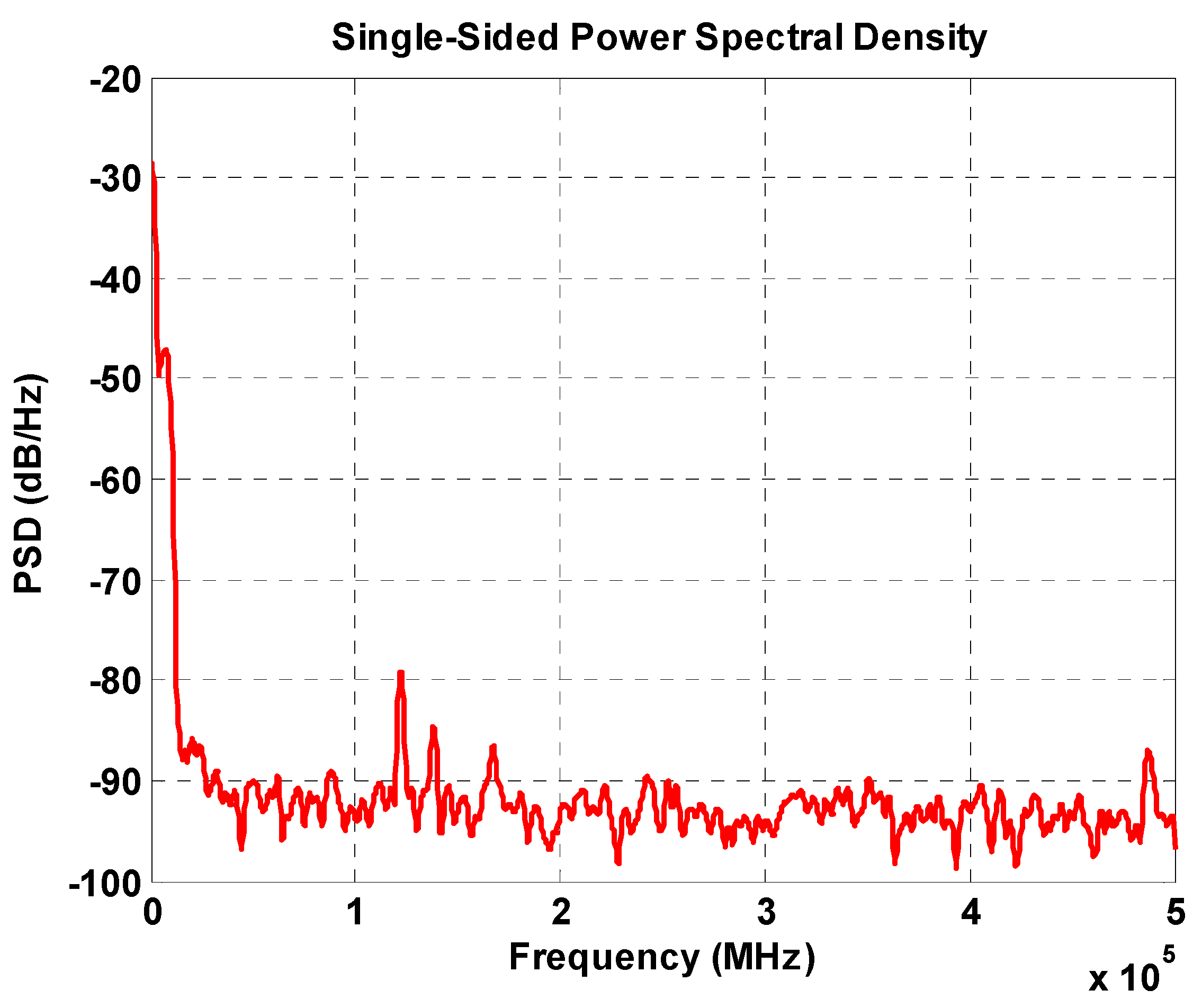
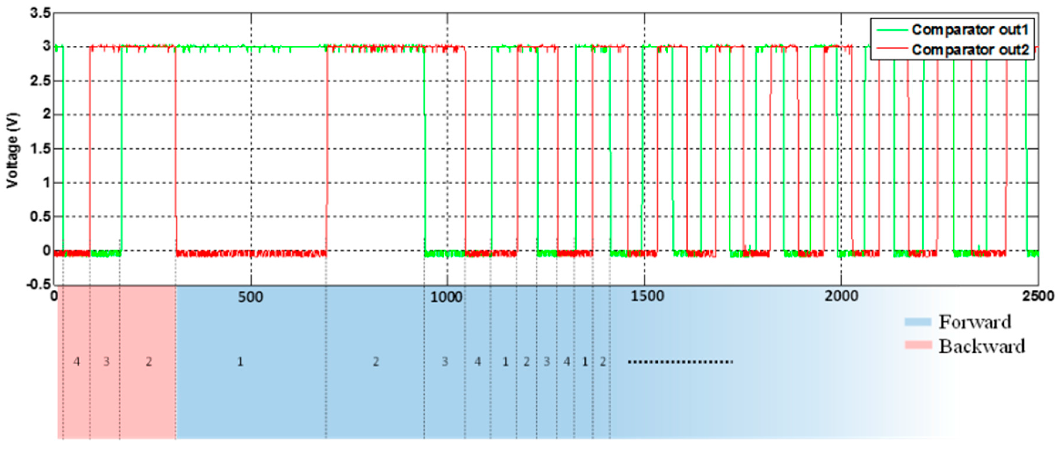
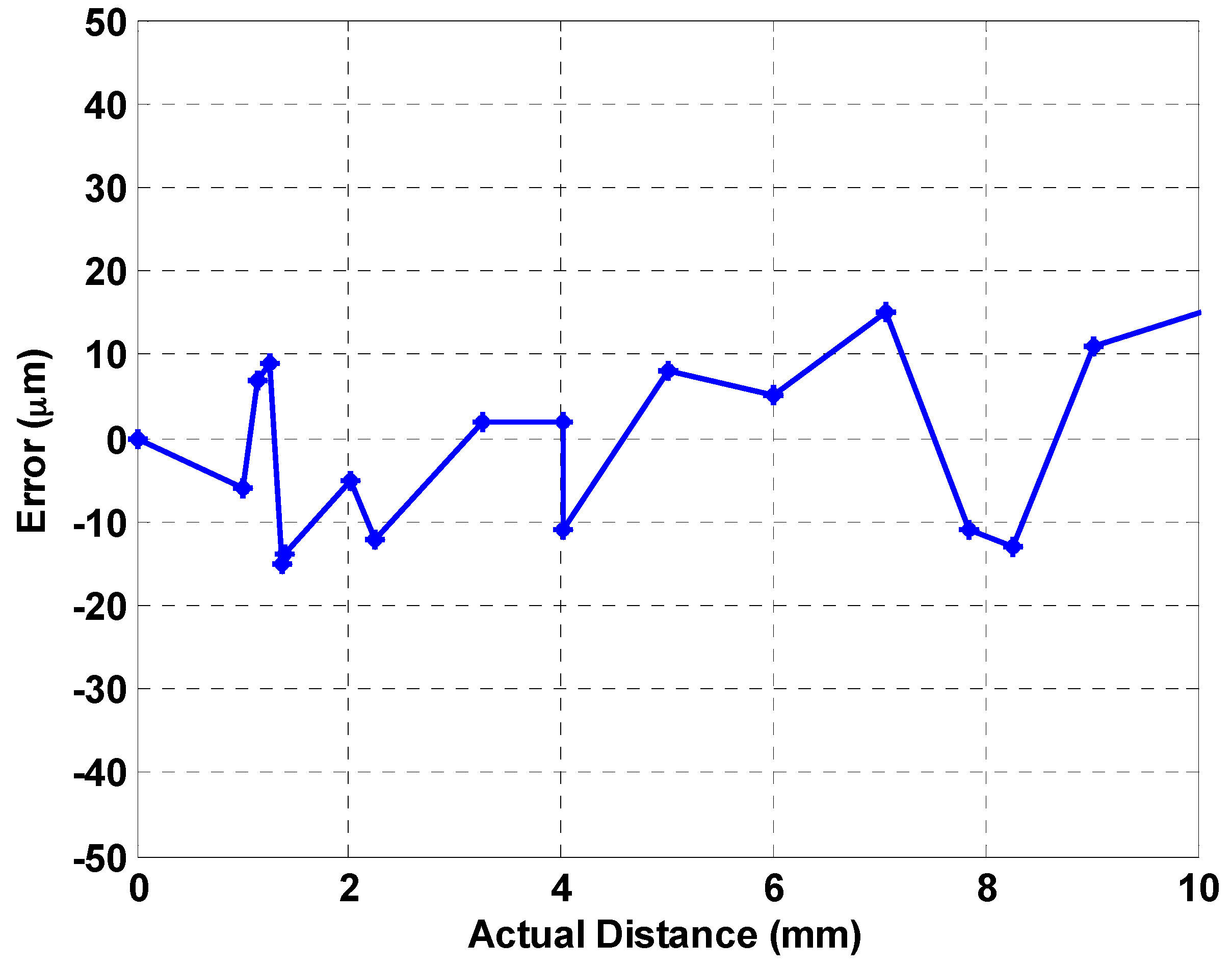
3. Experimental Results
4. Conclusions
Acknowledgments
Author Contributions
Conflicts of Interest
References
- Bazzi, A.M.; Dominguez-Garcia, A.; Krein, P.T. Markov reliability modeling for induction motor drives under field-oriented control. IEEE Trans. Power Electron. 2012, 27, 534–546. [Google Scholar] [CrossRef]
- Kung, Y.S. Design and implementation of a high-performance PMLSM drives using DSP chip. IEEE Trans. Ind. Electron. 2008, 55, 1341–1351. [Google Scholar] [CrossRef]
- Mihalachi, M.; Mutschler, P. Position acquisition for long primary linear drives with passive vehicles. In Proceedings of the IEEE Industry Applications Society Annual Meeting, IAS’08, Edmonton, AL, Canada, 5–9 October 2008; pp. 501–504.
- Emura, T.; Wang, L. A High-Resolution Interpolator for Incremental Encoders Based on the Quadrature PLL Method. IEEE Trans. Ind. Electron. 2000, 47, 84–90. [Google Scholar] [CrossRef]
- Hoang, H.V.; Le, H.T.; Jeon, J.W. A new approach based-on advanced adaptive digital PLL for improving the resolution and accuracy of magnetic encoders. In Proceedings of the IEEE/RSJ International Conference Intelligent Robots and Systems, Nice, France, 22–26 September 2008; pp. 3318–3323.
- Hagiwara, N.; Suzuki, Y.; Murase, H. A method of improving the resolution and accuracy of rotary encoders using a code compensation technique. IEEE Trans. Instrum. Meas. 1992, 41, 98–101. [Google Scholar] [CrossRef]
- Kim, J.C.; Hwang, S.H.; Kim, J.M.; Kim, C.U.; Choi, C. Ultra precise position estimation of servomotor using analog quadrature encoder. J. Power Electron. 2006, 6, 139–145. [Google Scholar]
- Mayer, J.R.R. High-resolution of rotary encoder analog quadrature signals. IEEE Trans. Instrum. Meas. 1994, 43, 494–498. [Google Scholar] [CrossRef]
- Xiao, K.; Wang, L. Analysis and error compensation of electric sine/cosine encoder. In Proceedings of the the Ninth International Conference on Electronic Measurement & Instruments, ICEMI 2009, Beijing, China, 16–19 August 2009; pp. 87–90.
- Ben-brahim, L.; Benammar, M.; Alhamadi, M.A. A novel converter for sinusoidal encoders. In Proceedings of the 5th IEEE Conference on Sensors, Daegu, Korea, 22–25 October 2006; pp. 1415–1418.
- Krau, M.; Leuschner, U.; Schniek, H.G. A 5V CMOS chip for interpolation of sine/cosine signals. In Proceedings of the 23rd European Solid-State Circuits Conference, ESSCIRC ‘97, Southampton, UK, 16–18 September 1997; pp. 336–339.
- Yien, C. Incremental encoder errors: Causes and methods to reduce them. In Proceedings of the PCIM’92, Nürnberg, Germany, 28–30 April 1992; pp. 110–121.
- Tan, K.K.; Zhou, H.X.; Lee, T.H. New interpolation method for quadrature encoder signals. IEEE Trans. Instrum. Meas. 2002, 51, 1073–1079. [Google Scholar] [CrossRef]
- Hsu, C.C.; Wu, J.T. A highly linear 125-MHz CMOS switched-resistor programmable gain amplifier. IEEE J. Solid-State Circuits 2003, 38, 1663–1670. [Google Scholar]
- Watanable, O.; Otaka, S.; Ashida, M.; Itakura, T. A 380-MHz CMOS linear-in-dB signal-summing variable gain amplifier with gain compensation techniques for CDMA systems. In Proceedings of the Symposium on VLSI Circuits Digest of Technical Papers, Honolulu, HI, USA, 13–15 June 2002; pp. 136–139.
- Khoury, J.M. On the design of constant settling time AGC circuits. IEEE Trans. Circuits Syst. 1998, 45, 283–294. [Google Scholar] [CrossRef]
- Gomez, R.; Abidi, A. A 50 MHz CMOS variable gain amplifier for magnetic data storage systems. IEEE J. Solid-State Circuits 1992, 27, 935–939. [Google Scholar] [CrossRef]
- Castello, R.; Gray, P.R. A high-performance micropower switch-capacitor filter. IEEE J. Solid-State Circuits 1982, 20, 1122–1132. [Google Scholar] [CrossRef]
- Garrity, D.; Rakers, P. Common-Mode Output Sensing Circuits. U.S. Patent 5 894 284, 13 April 1999. [Google Scholar]
- Carusone, T.C.; Johns, D.A.; Martin, K.W. Analog Integrated Circuit Design, 2nd ed.; John Wiley & Sons, Inc.: Hoboken, NJ, USA, 1997. [Google Scholar]
- Promitzer, G. 12-bit low power fully differential switched capacitor non-calibrating successive approximation ADC with 1MS/s. IEEE J. Solid-State Circuits 2001, 36, 1138–1143. [Google Scholar] [CrossRef]
- Abo, A.M.; Gray, P.R. A 1.5-V, 10-bit, 14.3-MS/s CMOS pipeline analog-to-digital converter. IEEE J. Solid-State Circuits 1999, 34, 599–606. [Google Scholar] [CrossRef]
- Yu, L.; Zhang, J.Y.; Wang, L.; Lu, J.G. A 12-bit Fully Differential SAR ADC with Dynamic Latch Comparator for Portable Physiological Monitoring Applications. Bull. Adv. Technol. Res. 2011, 5, 576–579. [Google Scholar]
- Liu, C.C. A 10-bit 50-MS/s SAR ADC with a Monotonic Capacitor Switching Procedure. IEEE J. Solid-State Circuits 2010, 45, 731–740. [Google Scholar] [CrossRef]
- Fang, X.; Srinivasan, V. CMOS 12 bits 50kS/s Micropower SAR and Dual-Slope Hybrid ADC. In Proceedings of the 52nd IEEE International Midwest Symposium on Circuits and Systems, MWSCAS ‘09, Cancun, Mexico, 2–5 August 2009; pp. 180–183.
- Balasubramaniam, H.; Galjan, W. 12-bit Hybrid C2C DAC based SAR ADC with Floating Voltage Shield. In Proceedings of the International Conference on Circuits and Systems, Medenine, Tunisia, 6–8 November 2009; pp. 1–5.
- Hsieh, S.E.; Ho, C.K.; Hsieh, C.C. A 1.2V 1MS/s 7.65fJ/Conversion-step 12-bit Hybrid, SAR ADC with time-to-Digital Converter. In Proceedings of the 2015 IEEE International Symposium on Circuits and Systems (ISCAS), Lisbon, Portugal, 24–27 May 2015; pp. 2429–2432.
- Baschirotto, A.; Dallago, E.; Malcovati, P.; Marchesi, M.; Melissano, E.; Morelli, M.; Siciliano, P.; Venchi, G. An Integrated Micro-Fluxgate Magnetic Sensor with Front-End Circuitry. IEEE Trans Instrum. Meas. 2009, 58, 3269–3275. [Google Scholar] [CrossRef]
- Chiang, C.-T.; Hsieh, K.-C.; Huang, Y.-C. Design of a CMOS phase to digital transducer for optical incremental sensors. Sens. Actuators A Phys. 2011, 170, 106–113. [Google Scholar] [CrossRef]


| [5] | [28] | [29] | This Work | |
|---|---|---|---|---|
| Technology | N/A | 0.35-μm CMOS | 0.5-μm CMOS 2P2M | 0.35-μm CMOS 2P4M |
| Interpolation Method | Advanced Adaptive Phase-locked loop | ADC | Comparator-based | ADC and comparator |
| Sampling Rate | N/A | 100 kS/s | Not needed | 600 kS/s |
| Interpolation Factor | 200 | - | 5, 10, 40 (optional) | 1000 (magnetic) |
| Output Format | Sine signal | Counter code | Pulse stream | Counter code |
| Chip Area | N/A | 1.7 mm2 | 3 mm2 | 6.61 mm2 |
| Power | N/A | 90 mW | 50 mW | 56 mW |
© 2016 by the authors; licensee MDPI, Basel, Switzerland. This article is an open access article distributed under the terms and conditions of the Creative Commons Attribution (CC-BY) license (http://creativecommons.org/licenses/by/4.0/).
Share and Cite
Tran, T.-H.; Chao, P.C.-P.; Chien, P.-C. The Front-End Readout as an Encoder IC for Magneto-Resistive Linear Scale Sensors. Sensors 2016, 16, 1416. https://doi.org/10.3390/s16091416
Tran T-H, Chao PC-P, Chien P-C. The Front-End Readout as an Encoder IC for Magneto-Resistive Linear Scale Sensors. Sensors. 2016; 16(9):1416. https://doi.org/10.3390/s16091416
Chicago/Turabian StyleTran, Trong-Hieu, Paul Chang-Po Chao, and Ping-Chieh Chien. 2016. "The Front-End Readout as an Encoder IC for Magneto-Resistive Linear Scale Sensors" Sensors 16, no. 9: 1416. https://doi.org/10.3390/s16091416